 | –≠–ª–µ–∫—Ç—Ä–æ–Ω–Ω—ã–π –∫–æ–º–ø–æ–Ω–µ–Ω—Ç: OPA2237 | –°–∫–∞—á–∞—Ç—å:  PDF PDF  ZIP ZIP |

FEATURES
q
MICRO-SIZE, MINIATURE PACKAGES
Single: SOT-23-5, SO-8
Dual: MSOP-8, SO-8
Quad: SSOP-16
q
LOW OFFSET VOLTAGE: 750
µ
V max
q
WIDE SUPPLY RANGE
Single Supply: +2.7V to +36V
Dual Supply:
±
1.35V to
±
18V
q
LOW QUIESCENT CURRENT: 350
µ
A max
q
WIDE BANDWIDTH: 1.5MHz
DESCRIPTION
The OPA237 op amp family is one of Burr-Brown's
Micro
Amplifier
TM
series of miniature products. In addi-
tion to small size, these devices feature low offset
voltage, low quiescent current, low bias current, and a
wide supply range. Single, dual, and quad versions
have identical specifications for maximum design flex-
ibility. They are ideal for single supply, battery oper-
ated, and space-limited applications, such as PCMCIA
cards and other portable instruments.
OPA237 series op amps can operate from either single
or dual supplies. When operated from a single supply,
the input common-mode range extends below ground
and the output can swing to within 10mV of ground.
Dual and quad designs feature completely indepen-
dent circuitry for lowest crosstalk and freedom from
interaction.
Single, dual, and quad are offered in space-saving
surface-mount packages. The single version is available
in the ultra-miniature 5-lead SOT-23-5 and SO-8 sur-
face-mount. The dual version comes in a miniature
MSOP-8 and SO-8 surface-mount. The quad is avail-
able in an SSOP-16. The SSOP-16 has the same body
size as an SO-8 with 16 leads, while the MSOP-8 has the
same lead count as a SO-8 but half the size. The
SOT-23-5 is even smaller at one-fourth the size of an
SO-8. All are specified for ≠40
∞
C to +85
∞
C operation. A
macromodel is available for design analysis.
APPLICATIONS
q
BATTERY POWERED INSTRUMENTS
q
PORTABLE DEVICES
q
PCMCIA CARDS
q
MEDICAL INSTRUMENTS
q
TEST EQUIPMENT
OPA237
OPA2237
OPA4237
Æ
SINGLE-SUPPLY OPERATIONAL AMPLIFIERS
Micro
Amplifier
TM
Series
International
Airport
Industrial
Park
∑
Mailing
Address:
PO
Box
11400,
Tucson,
AZ
85734
∑
Street
Address:
6730
S.
Tucson
Blvd.,
Tucson,
AZ
85706
∑
Tel:
(520)
746-1111
∑
Twx:
910-952-1111
Internet:
http://www.burr-brown.com/
∑
FAXLine:
(800)
548-6133
(US/Canada
Only)
∑
Cable:
BBRCORP
∑
Telex:
066-6491
∑
FAX:
(520)
889-1510
∑
Immediate
Product
Info:
(800)
548-6132
© 1996 Burr-Brown Corporation
PDS-1327B
Printed in U.S.A. October, 1996
1
2
3
4
5
6
7
8
16
15
14
13
12
11
10
9
Out D
≠In D
+In D
V≠
+In C
≠In C
Out C
NC
Out A
≠In A
+In A
V+
+In B
≠In B
Out B
NC
OPA4237
SSOP-16
A
D
B
C
1
2
3
4
8
7
6
5
NC
V+
Output
NC
NC
≠In
+In
V≠
OPA237
SO-8
1
2
3
4
8
7
6
5
V+
Out B
≠In B
+In B
Out A
≠In A
+In A
V≠
OPA2237
SO-8, MSOP-8
A
B
1
2
3
5
4
V+
≠In
Out
V≠
+In
OPA237
SOT-23-5
SSOP-16
quad
SO-8
single/dual
MSOP dual
SOT-23-5
single
SBOS057

2
Æ
OPA237, 2237, 4237
The information provided herein is believed to be reliable; however, BURR-BROWN assumes no responsibility for inaccuracies or omissions. BURR-BROWN assumes
no responsibility for the use of this information, and all use of such information shall be entirely at the user's own risk. Prices and specifications are subject to change
without notice. No patent rights or licenses to any of the circuits described herein are implied or granted to any third party. BURR-BROWN does not authorize or warrant
any BURR-BROWN product for use in life support devices and/or systems.
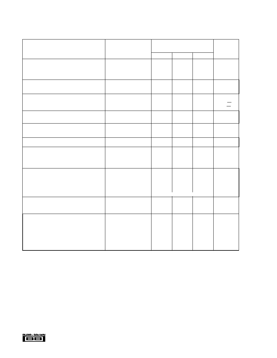
SPECIFICATIONS: V
S
= +5V
At T
A
= +25
∞
C, V
S
= +5V, R
L
= 10k
connected to V
S
/2, unless otherwise noted.
OPA237UA, NA
OPA2237UA, EA
OPA4237UA
PARAMETER
CONDITION
MIN
TYP
MAX
UNITS
OFFSET VOLTAGE
Input Offset Voltage
V
CM
= 2.5V
±
250
±
750
µ
V
vs Temperature
(1)
Specified Temperature Range
±
2
±
5
µ
V/
∞
C
vs Power Supply (PSRR)
V
S
= +2.7V to +36V
10
30
µ
V/V
Channel Separation (dual and quad)
0.5
µ
V/V
INPUT BIAS CURRENT
Input Bias Current
(2)
V
CM
= 2.5V
≠10
≠40
nA
Input Offset Current
V
CM
= 2.5V
±
0.5
±
10
nA
NOISE
Input Voltage Noise, f = 0.1 to 10Hz
1
µ
Vp-p
Input Voltage Noise Density, f = 1kHz
28
nV/
Hz
Current Noise Density, f = 1kHz
60
fA/
Hz
INPUT VOLTAGE RANGE
Common-Mode Voltage Range
≠0.2
(V+) ≠1.5
V
Common-Mode Rejection
V
CM
= ≠0.2V to 3.5V
78
86
dB
INPUT IMPEDANCE
Differential
5 ∑ 10
6
|| 4
|| pF
Common-Mode
5 ∑ 10
9
|| 2
|| pF
OPEN-LOOP GAIN
Open-Loop Voltage Gain
V
O
= 0.5V to 4V
80
88
dB
FREQUENCY RESPONSE
Gain-Bandwidth Product
1.4
MHz
Slew Rate
G = 1
0.5
V/
µ
s
Settling Time: 0.1%
G = ≠1, 3V Step, C
L
= 100pF
11
µ
s
0.01%
G = ≠1, 3V Step, C
L
= 100pF
16
µ
s
OUTPUT
Voltage Output, Positive
R
L
= 100k
to Ground
(V+) ≠1
(V+) ≠0.75
V
Negative
R
L
= 100k
to Ground
0.01
0.001
V
Positive
R
L
= 100k
to 2.5V
(V+) ≠1
(V+) ≠0.75
V
Negative
R
L
= 100k
to 2.5V
0.12
0.04
V
Positive
R
L
= 10k
to 2.5V
(V+) ≠1
(V+) ≠0.75
V
Negative
R
L
= 10k
to 2.5V
0.5
0.35
V
Short-Circuit Current
≠10/+4
mA
Capacitive Load Drive (stable operation)
See Typical Curves
POWER SUPPLY
Specified Operating Voltage
+5
V
Operating Range
+2.7
+36
V
Quiescent Current (per amplifier)
170
350
µ
A
TEMPERATURE RANGE
Specified Range
≠40
+85
∞
C
Operating Range
≠55
+125
∞
C
Storage
≠55
+125
∞
C
Thermal Resistance,
JA
5-Lead SOT-23-5
200
∞
C/W
MSOP-8 Surface-Mount
150
∞
C/W
SSOP-16 Surface-Mount
150
∞
C/W
SO-8 Surface-Mount
150
∞
C/W
NOTES: (1) Guaranteed by wafer-level test to 95% confidence. (2) Positive conventional current flows into the input terminals.

3
OPA237, 2237, 4237
Æ
SPECIFICATIONS: V
S
= +2.7V
At T
A
= +25
∞
C, V
S
= +2.7V, R
L
= 10k
connected to V
S
/2, unless otherwise noted.
OPA237UA, NA
OPA2237UA, EA
OPA4237UA
PARAMETER
CONDITION
MIN
TYP
MAX
UNITS
OFFSET VOLTAGE
Input Offset Voltage
V
CM
= 1V
±
250
±
750
µ
V
vs Temperature
(1)
Specified Temperature Range
±
2
±
5
µ
V/
∞
C
vs Power Supply (PSRR)
V
S
= +2.7V to +36V
10
30
µ
V/V
Channel Separation (dual and quad)
0.5
µ
V/V
INPUT BIAS CURRENT
Input Bias Current
(2)
V
CM
= 1V
≠10
≠40
nA
Input Offset Current
V
CM
= 1V
±
0.5
±
10
nA
NOISE
Input Voltage Noise, f = 0.1 to 10Hz
1
µ
Vp-p
Input Voltage Noise Density, f = 1kHz
28
nV/
Hz
Current Noise Density, f = 1kHz
60
fA/
Hz
INPUT VOLTAGE RANGE
Common-Mode Voltage Range
≠0.2
(V+) ≠1.5
V
Common-Mode Rejection
V
CM
= ≠0.2V to 1.2V
75
85
dB
INPUT IMPEDANCE
Differential
5 ∑ 10
6
|| 4
|| pF
Common-Mode
5 ∑ 10
9
|| 2
|| pF
OPEN-LOOP GAIN
Open-Loop Voltage Gain
V
O
= 0.5V to 1.7V
80
88
dB
FREQUENCY RESPONSE
Gain-Bandwidth Product
1.2
MHz
Slew Rate
G = 1
0.5
V/
µ
s
Settling Time: 0.1%
G = ≠1, 1V Step, C
L
= 100pF
5
µ
s
0.01%
G = ≠1, 1V Step, C
L
= 100pF
8
µ
s
OUTPUT
Voltage Output, Positive
R
L
= 100k
to Ground
(V+) ≠1
(V+) ≠0.75
V
Negative
R
L
= 100k
to Ground
0.01
0.001
V
Positive
R
L
= 100k
to 1.35V
(V+) ≠1
(V+) ≠0.75
V
Negative
R
L
= 100k
to 1.35V
0.06
0.02
V
Positive
R
L
= 10k
to 1.35V
(V+) ≠1
(V+) ≠0.75
V
Negative
R
L
= 10k
to 1.35V
0.3
0.2
V
Short-Circuit Current
≠5/+3.5
mA
Capacitive Load Drive (stable operation)
See Typical Curves
POWER SUPPLY
Specified Operating Voltage
+2.7
V
Operating Range
+2.7
+36
V
Quiescent Current (per amplifier)
160
350
µ
A
TEMPERATURE RANGE
Specified Range
≠40
+85
∞
C
Operating Range
≠55
+125
∞
C
Storage
≠55
+125
∞
C
Thermal Resistance,
JA
5-Lead SOT-23-5
200
∞
C/W
MSOP-8 Surface-Mount
150
∞
C/W
SSOP-16 Surface-Mount
150
∞
C/W
SO-8 Surface-Mount
150
∞
C/W
NOTES: (1) Guaranteed by wafer-level test to 95% confidence. (2) Positive conventional current flows into the input terminals.
4
Æ
OPA237, 2237, 4237
SPECIFICATIONS: V
S
=
±
15V
At T
A
= +25
∞
C, V
S
=
±
15V, R
L
= 10k
connected to V
S
/2, unless otherwise noted.
OPA237UA, NA
OPA2237UA, EA
OPA4237UA
PARAMETER
CONDITION
MIN
TYP
MAX
UNITS
OFFSET VOLTAGE
Input Offset Voltage
V
CM
= 0V
±
350
±
950
µ
V
vs Temperature
(1)
Specified Temperature Range
±
2.5
±
7
µ
V/
∞
C
vs Power Supply (PSRR)
V
S
=
±
1.35V to
±
18V
10
30
µ
V/V
Channel Separation (dual and quad)
0.5
µ
V/V
INPUT BIAS CURRENT
Input Bias Current
(2)
V
CM
= 0V
≠8.5
≠40
nA
Input Offset Current
V
CM
= 0V
±
0.5
±
10
nA
NOISE
Input Voltage Noise, f = 0.1 to 10Hz
1
µ
Vp-p
Input Voltage Noise Density, f = 1kHz
28
nV/
Hz
Current Noise Density, f = 1kHz
60
fA/
Hz
INPUT VOLTAGE RANGE
Common-Mode Voltage Range
(V≠) ≠0.2
(V+) ≠1.5
V
Common-Mode Rejection
V
CM
= ≠15V to 13.5V
80
90
dB
INPUT IMPEDANCE
Differential
5 ∑ 10
6
|| 4
|| pF
Common-Mode
5 ∑ 10
9
|| 2
|| pF
OPEN-LOOP GAIN
Open-Loop Voltage Gain
V
O
= ≠14V to 13.8V
80
88
dB
FREQUENCY RESPONSE
Gain-Bandwidth Product
1.5
MHz
Slew Rate
G = 1
0.5
V/
µ
s
Settling Time: 0.1%
G = ≠1, 10V Step, C
L
= 100pF
18
µ
s
0.01%
G = ≠1, 10V Step, C
L
= 100pF
21
µ
s
OUTPUT
Voltage Output, Positive
R
L
= 100k
(V+) ≠1.2
(V+) ≠0.9
V
Negative
R
L
= 100k
(V≠) +0.5
(V≠) +0.3
V
Positive
R
L
= 10k
(V+) ≠1.2
(V+) ≠0.9
V
Negative
R
L
= 10k
(V≠) +1
(V≠) +0.85
V
Short-Circuit Current
≠8/+4.5
mA
Capacitive Load Drive (stable operation)
See Typical Curves
POWER SUPPLY
Specified Operating Voltage
±
15
V
Operating Range
±
1.35
±
18
V
Quiescent Current (per amplifier)
±
200
±
475
µ
A
TEMPERATURE RANGE
Specified Range
≠40
+85
∞
C
Operating Range
≠55
+125
∞
C
Storage
≠55
+125
∞
C
Thermal Resistance,
JA
5-Lead SOT-23-5
200
∞
C/W
MSOP-8 Surface-Mount
150
∞
C/W
SSOP-16 Surface-Mount
150
∞
C/W
SO-8 Surface-Mount
150
∞
C/W
NOTES: (1) Guaranteed by wafer-level test to 95% confidence. (2) Positive conventional current flows into the input terminals.
5
OPA237, 2237, 4237
Æ
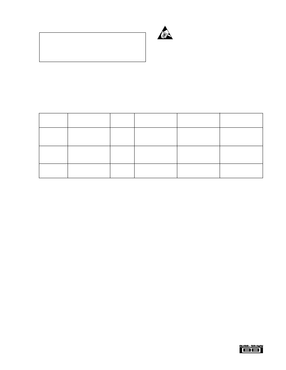
PACKAGE
DRAWING
TEMPERATURE
PACKAGE
ORDERING
PRODUCT
PACKAGE
NUMBER
(1)
RANGE
MARKING
NUMBER
(2)
Single
OPA237NA
5-Lead SOT-23-5
331
≠40
∞
C to +85
∞
C
A37A
OPA237NA-250
"
"
"
"
"
OPA237NA-3K
OPA237UA
SO-8 Surface-Mount
182
≠40
∞
C to +85
∞
C
OPA237UA
OPA237UA
Dual
OPA2237EA
MSOP-8 Surface-Mount
337
≠40
∞
C to +85
∞
C
B37A
OPA2237EA-250
"
"
"
"
"
OPA2237EA-2500
OPA2237UA
SO-8 Surface-Mount
182
≠40
∞
C to +85
∞
C
OPA2237UA
OPA2237UA
Quad
OPA4237UA
SSOP-16 Surface-Mount
322
≠40
∞
C to +85
∞
C
OPA4237UA
OPA4237UA-250
"
"
"
"
"
OPA4237UA-2500
NOTE: (1) For detailed drawing and dimension table, please see end of data sheet, or Appendix C of Burr-Brown IC Data Book. (2) Models with -250, -2500, and
-3K are available only in Tape and Reel in the quantity indicated (e.g., -250 indicates 250 devices per reel). Ordering 3000 pieces of "OPA237NA-3K" will get a
single 3000 piece Tape and Reel. SO-8 models are available in tubes or Tape and Reel. For detailed Tape and Reel mechanical information, refer to
Appendix B of Burr-Brown IC Data Book.
ELECTROSTATIC
DISCHARGE SENSITIVITY
This integrated circuit can be damaged by ESD. Burr-Brown
recommends that all integrated circuits be handled with
appropriate precautions. Failure to observe proper handling
and installation procedures can cause damage.
ESD damage can range from subtle performance degrada-
tion to complete device failure. Precision integrated circuits
may be more susceptible to damage because very small
parametric changes could cause the device not to meet its
published specifications.
Supply Voltage, V+ to V≠ ..................................................................... 36V
Input Voltage ....................................................... (V≠) ≠0.7V to (V+) +0.7V
Output Short-Circuit
(1) .......................................................................................
Continuous
Operating Temperature ................................................... ≠40
∞
C to +125
∞
C
Storage Temperature ...................................................... ≠55
∞
C to +125
∞
C
Junction Temperature .................................................................... +150
∞
C
Lead Temperature (soldering, 10s) .................................................. 300
∞
C
NOTE: (1) Short circuit to ground, one amplifier per package.
ABSOLUTE MAXIMUM RATINGS
PACKAGE/ORDERING INFORMATION
6
Æ
OPA237, 2237, 4237
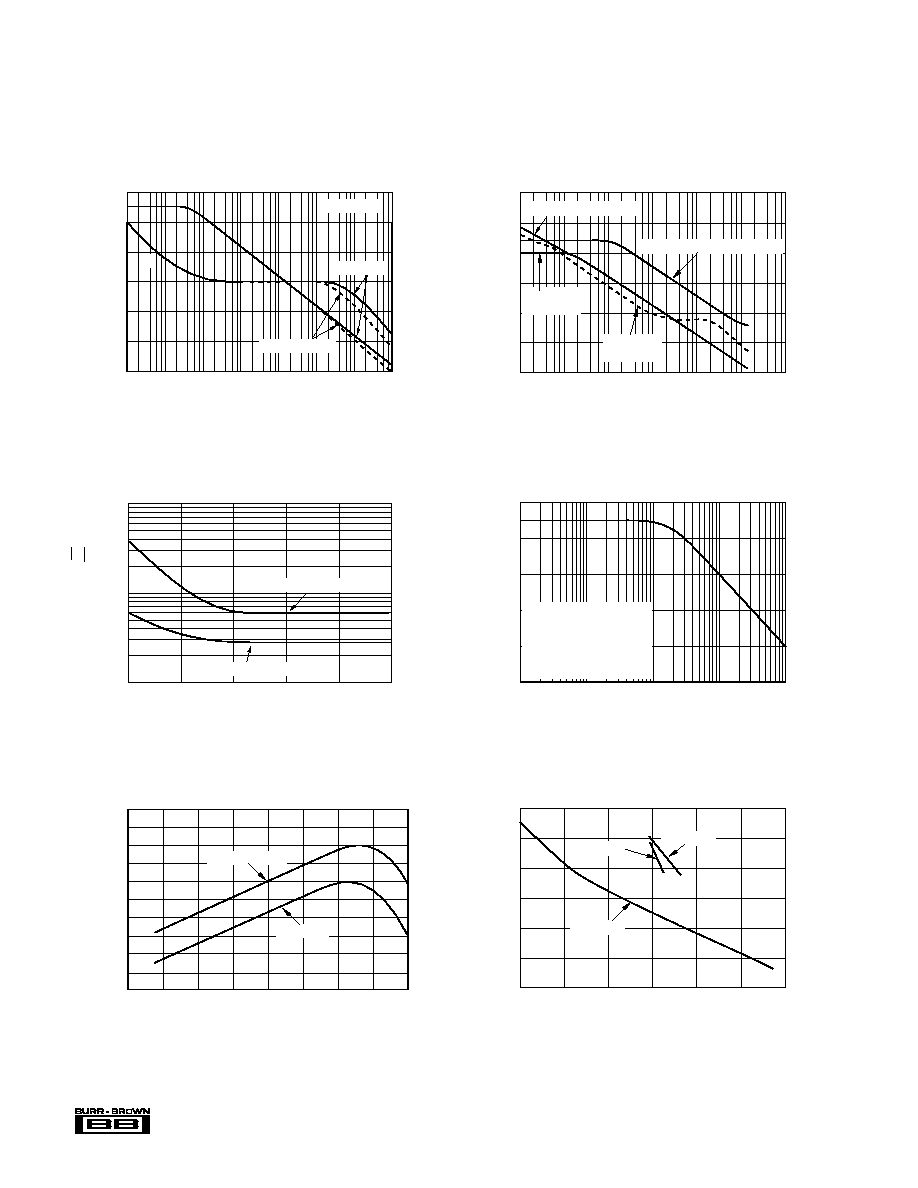
INPUT BIAS CURRENT
vs INPUT COMMON-MODE VOLTAGE
≠12
≠11
≠10
≠9
≠8
≠7
≠6
Input Bias Current (nA)
Common-Mode Voltage (V)
≠15
≠10
≠5
0
5
10
15
V
S
= ±15V
V
S
= +5V
V
S
= +2.7V
TYPICAL PERFORMANCE CURVES
At T
A
= +25
∞
C and R
L
= 10k
,
unless otherwise noted.
POWER SUPPLY and COMMON-MODE REJECTION
vs FREQUENCY
120
100
80
60
40
20
0
PSR, CMR (dB)
Frequency (Hz)
10
100
1k
10k
100k
1M
10M
+PSR (V
S
= +5V, ±15V)
CMR (V
S
= +2.7V, +5V or ±15V)
+PSR
(V
S
= +2.7V)
≠PSR
(V
S
= ±15V)
INPUT NOISE AND CURRENT NOISE
SPECTRAL DENSITY vs FREQUENCY
1
1k
100
10
Voltage Noise (nV/
Hz)
Current Noise (fA/
Hz)
Frequency (Hz)
10
100
1k
10k
100k
Current Noise
Voltage Noise
OPEN-LOOP GAIN/PHASE vs FREQUENCY
1
100
80
60
40
20
0
≠20
Voltage Gain (dB)
0
≠45
≠90
≠135
≠180
Phase (∞)
Frequency (Hz)
10
100
1k
10k
100k
1M
10M
C
L
= 100pF
V
S
= ±15V
V
S
= +2.7V, +5V
G
CHANNEL SEPARATION vs FREQUENCY
Frequency (Hz)
Channel Separation (dB)
130
120
110
100
90
80
10
100
1k
10k
100k
Dual and quad devices.
G = 1, all channels.
Quad measured channel
A to D or B to C--other
combinations yield improved
rejection.
INPUT BIAS CURRENT vs TEMPERATURE
Temperature (∞C)
Input Bias Current (nA)
14
12
10
8
6
4
≠75
≠50
≠25
0
25
50
75
100
125
V
S
= +2.7V, +5V
V
S
= ±15V
7
OPA237, 2237, 4237
Æ
TYPICAL PERFORMANCE CURVES
(CONT)
At T
A
= +25
∞
C and R
L
= 10k
,
unless otherwise noted.
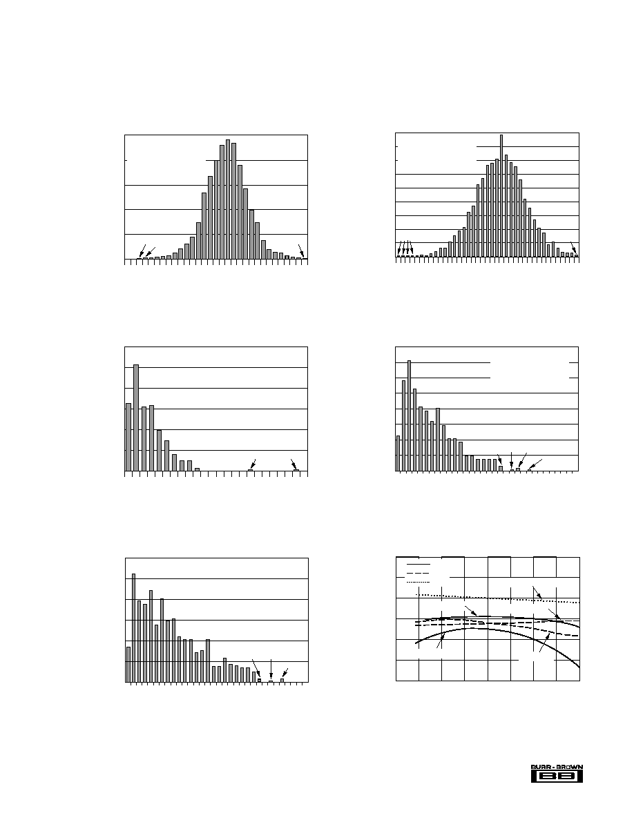
OFFSET VOLTAGE DRIFT
PRODUCTION DISTRIBUTION
Percent of Amplifiers (%)
Offset Voltage Drift (µV/∞C)
0.5
1.5
2.5
3.5
4.5
5.5
6.5
7.5
8.5
9.5
10.5
11.5
30
25
20
15
10
5
0
0.2%
0.2%
V
S
= +2.7V
Typical production
distribution of packaged
units. Single, dual,
and quad units included.
OFFSET VOLTAGE DRIFT
PRODUCTION DISTRIBUTION
Percent of Amplifiers (%)
Offset Voltage Drift (µV/∞C)
16
14
12
10
8
6
4
2
0
0.5
1.5
2
1
3
3.5
2.5
4
4.5
5
5.5
6
6.5
7
8
7.5
V
S
= +5V
0.4%
0.6%
0.2%
0.2%
Typical production
distribution of packaged
units. Single, dual,
and quad units included.
OFFSET VOLTAGE DRIFT
PRODUCTION DISTRIBUTION
Percent of Amplifiers (%)
Offset Voltage Drift (µV/∞C)
12
10
8
6
4
2
0
0.5
1.5
2
1
3
3.5
2.5
4
4.5
5
5.5
6
6.5
7
8
7.5
V
S
= ±15V
0.4%
0.4%
0.2%
Typical production
distribution of packaged
units. Single, dual,
and quad units included.
A
OL
, CMR, PSR vs TEMPERATURE
Temperature (∞C)
A
OL
, CMR, PSR (dB)
120
110
100
90
80
70
60
≠75
≠50
≠25
0
25
50
75
100
125
V
S
= +2.7V, +5V
V
S
= +2.7V, +5V
V
S
= +2.7V, +5V, ±15V
V
S
= ±15V
V
S
= ±15V
CMR
AOL
PSR
OFFSET VOLTAGE
PRODUCTION DISTRIBUTION
Percent of Amplifiers (%)
Offset Voltage (µV)
≠750
≠650
≠550
≠450
≠350
≠250
≠150
≠50
50
150
250
350
450
550
650
750
12.5
10
7.5
5
2.5
0
V
S
= +2.7V, +5V
0.2%
0.4%
0.7%
Typical production
distribution of packaged
units. Single, dual,
and quad units included.
OFFSET VOLTAGE
PRODUCTION DISTRIBUTION
Percent of Amplifiers (%)
Offset Voltage (µV)
≠950
≠850
≠750
≠650
≠550
≠450
≠350
≠250
≠150
≠50
50
150
250
350
450
550
650
750
850
950
9
8
7
6
5
4
3
2
1
0
V
S
= ±15V
0.1%
0.1%
Typical production
distribution of packaged
units. Single, dual,
and quad units included.
8
Æ
OPA237, 2237, 4237
70
60
50
40
30
20
10
0
10
100
1k
10k
Load Capacitance (pF)
Overshoot (%)
SMALL-SIGNAL OVERSHOOT
vs LOAD CAPACITANCE
G = +1, V
S
= +2.7V, +5V
G = +1, V
S
= ±15V
G = ≠1, V
S
= +2.7V, +5V
G = ≠1, V
S
= ±15V
G = ≠2, V
S
= +2.7V, +5V
G = ≠2, V
S
= ±15V
G = ≠10, V
S
= +2.7V,
+5V, ±15V
TYPICAL PERFORMANCE CURVES
(CONT)
At T
A
= +25
∞
C and R
L
= 10k
,
unless otherwise noted.
LARGE-SIGNAL STEP RESPONSE
G = 1, C
L
= 100pF, V
S
= +5V
10
µ
s/div
1V/div
SMALL-SIGNAL STEP RESPONSE
G = 1, C
L
= 100pF, V
S
= +5V
20mV/div
1
µ
s/div
SMALL-SIGNAL STEP RESPONSE
G = 1, C
L
= 220pF, V
S
= +5V
20mV/div
2
µ
s/div
OUTPUT VOLTAGE SWING vs OUTPUT CURRENT
V+
(V+) ≠0.5
(V+) ≠1
(V+) ≠1.5
(V+) ≠2
(V≠) +2
(V≠) +1.5
(V≠) +1
(V≠) +0.5
V≠
0
1
2
3
4
5
Output Current (mA)
Output Voltage Swing (V)
+125∞C
+25∞C
≠55∞C
+125∞C
+25∞C
+125∞C
≠55∞C
Sinking Current
Sourcing Current
SETTLING TIME vs GAIN
Gain (V/V)
Settling Time (µs)
100
10
1
≠1
≠10
≠100
0.01%
0.1%
V
S
= +2.7V,
1V Step
V
S
= ±15V,
10V Step
V
S
= +5V,
3V Step
9
OPA237, 2237, 4237
Æ
TYPICAL PERFORMANCE CURVES
(CONT)
At T
A
= +25
∞
C and R
L
= 10k
,
unless otherwise noted.
MAXIMUM OUTPUT VOLTAGE
vs FREQUENCY
1M
100k
Frequency (Hz)
1k
10k
30
25
20
15
10
5
0
Output Voltage (Vp-p)
Maximum output voltage
without slew-rate induced
distortion
V
S
= ±15V
V
S
= +5V
V
S
= +2.7V
QUIESCENT CURRENT vs TEMPERATURE
Temperature (∞C)
Quiescent Current (
µ
A)
300
250
200
150
100
50
≠75
≠50
≠25
0
25
50
75
100
125
V
S
= +5V
V
S
= +2.7V
V
S
= ±15V
SHORT-CIRCUIT CURRENT vs TEMPERATURE
Temperature (∞C)
Short-Circuit Current (mA)
12
10
8
6
4
2
0
≠75
≠50
≠25
0
25
50
I
SC
_
I
SC
+
75
100
125
V
S
= +2.7V
V
S
= +5V
V
S
= ±15V
V
S
= +2.7V
V
S
= ±15V
V
S
= +5V
10
Æ
OPA237, 2237, 4237
APPLICATIONS INFORMATION
OPA237 series op amps are unity-gain stable and suitable
for a wide range of general-purpose applications. Power
supply pins should be bypassed with 10nF ceramic capaci-
tors.
OPERATING VOLTAGE
OPA237 series op amps operate from single (+2.7V to
+36V) or dual (
±
1.35V to
±
18V) supplies with excellent
performance. Most behavior remains unchanged through-
out the full operating voltage range. Parameters which
vary significantly with operating voltage are shown in
typical performance curves. Specifications are production
tested with +2.7V, +5V, and
±
15V supplies.
OUTPUT CURRENT AND STABILITY
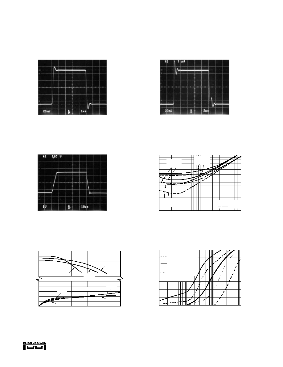
OPA237 series op amps can drive large capacitive loads.
However, under certain limited output conditions any op
amp may become unstable. Figure 1 shows the region
where the OPA237 has a potential for instability. These
load conditions are rarely encountered, especially for single
supply applications. For example, take the case when a
+5V supply with a 10k
load to V
S
/2 is used. OPA237
series op amps remain stable with capacitive loads up to
4,000pF, if sinking current and up to 10,000pF, if sourcing
current. Furthermore, in single supply applications where
the load is connected to ground, the op amp is only
sourcing current, and as shown in Figure 1, can drive
10,000pF with output currents up to 1.5mA.
FIGURE 1. Stability-Capacitive Load vs Output Current.
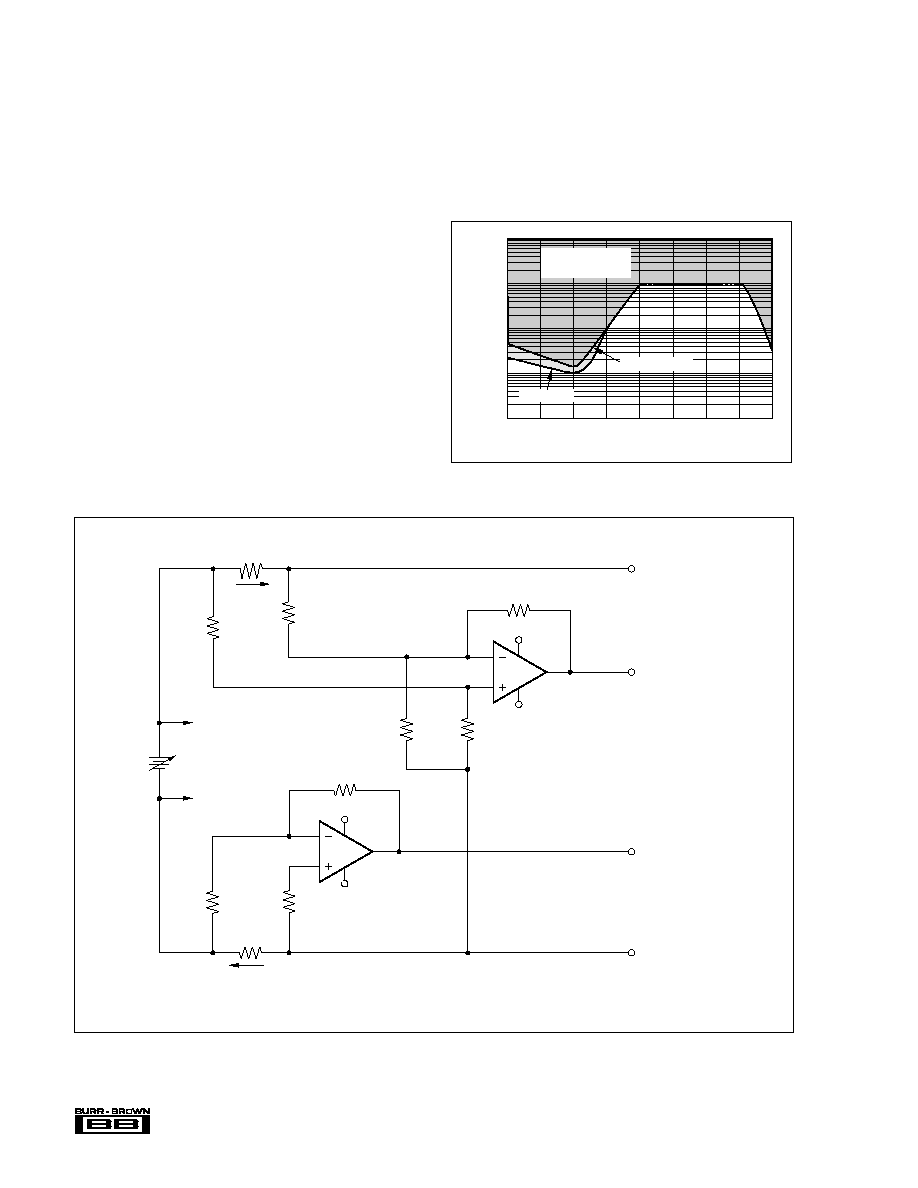
FIGURE 2. Low and High-Side Battery Current Sensing.
R
L
10
A1
OPA237
+
R
1
38.3k
R
3
38.3k
R
5
383k
R
6
10k
R
7
9.09k
R
4
20k
R
2
19.1k
A2
OPA237
R
8
100k
R
H
10
I
H
V+
V≠
V+
V≠
2.7V to ±15V
V+ for A
1
, A
2
≠In
+In
≠In
+In
V
O
= 10 ∑ I
H
∑ R
H
To Load
To Load
V
O
= 10 ∑ I
L
∑ R
L
Common-mode range of A2
extends to V≠ for low-side sensing.
Optional for I
B
Cancellation
(R
7
= R
6
II R
8
)
R
2
and R
4
divide down the
common-mode input to A1.
Low-Side
Current Sense
High-Side
Current Sense
Out
Out
NOTE: Low and high-side sensing circuits can be used independently.
V≠ for A
1
, A
2
I
L
2
0.5
1
1.5
Output Current (mA)
≠2
≠1.5
≠1
≠0.5
0
100k
10k
1k
100
10
Capacitive Load (pF)
V
S
= +2.7V
V
S
= +5V, ±15V
OPERATION NOT
RECOMMENDED

IMPORTANT NOTICE
Texas Instruments and its subsidiaries (TI) reserve the right to make changes to their products or to discontinue
any product or service without notice, and advise customers to obtain the latest version of relevant information
to verify, before placing orders, that information being relied on is current and complete. All products are sold
subject to the terms and conditions of sale supplied at the time of order acknowledgment, including those
pertaining to warranty, patent infringement, and limitation of liability.
TI warrants performance of its semiconductor products to the specifications applicable at the time of sale in
accordance with TI's standard warranty. Testing and other quality control techniques are utilized to the extent
TI deems necessary to support this warranty. Specific testing of all parameters of each device is not necessarily
performed, except those mandated by government requirements.
Customers are responsible for their applications using TI components.
In order to minimize risks associated with the customer's applications, adequate design and operating
safeguards must be provided by the customer to minimize inherent or procedural hazards.
TI assumes no liability for applications assistance or customer product design. TI does not warrant or represent
that any license, either express or implied, is granted under any patent right, copyright, mask work right, or other
intellectual property right of TI covering or relating to any combination, machine, or process in which such
semiconductor products or services might be or are used. TI's publication of information regarding any third
party's products or services does not constitute TI's approval, warranty or endorsement thereof.
Copyright
©
2000, Texas Instruments Incorporated