
1
Æ
OPA241, 2241, 4241
OPA251, 2251, 4251
Æ
OPA251
OPA2251
OPA4251
© 1997 Burr-Brown Corporation
PDS-1406B
Printed in U.S.A. October, 1998
International Airport Industrial Park ∑ Mailing Address: PO Box 11400, Tucson, AZ 85734 ∑ Street Address: 6730 S. Tucson Blvd., Tucson, AZ 85706 ∑ Tel: (520) 746-1111 ∑ Twx: 910-952-1111
Internet: http://www.burr-brown.com/ ∑ FAXLine: (800) 548-6133 (US/Canada Only) ∑ Cable: BBRCORP ∑ Telex: 066-6491 ∑ FAX: (520) 889-1510 ∑ Immediate Product Info: (800) 548-6132
Single-Supply,
Micro
POWER
OPERATIONAL AMPLIFIERS
FEATURES
q
Micro
POWER: I
Q
= 25
µ
A
q
SINGLE-SUPPLY OPERATION
q
RAIL-TO-RAIL OUTPUT (within 50mV)
q
WIDE SUPPLY RANGE
Single Supply: +2.7V to +36V
Dual Supply:
±
1.35V to
±
18V
q
LOW OFFSET VOLTAGE:
±
250
µ
V max
q
HIGH COMMON-MODE REJECTION: 124dB
q
HIGH OPEN-LOOP GAIN: 128dB
q
SINGLE, DUAL, AND QUAD
DESCRIPTION
The OPA241 series and OPA251 series are specifically
designed for battery powered, portable applications. In addi-
tion to very low power consumption (25
µ
A), these amplifi-
ers feature low offset voltage, rail-to-rail output swing, high
common-mode rejection, and high open-loop gain.
The OPA241 series is optimized for operation at low power
supply voltage while the OPA251 series is optimized for
high power supplies. Both can operate from either single
(+2.7V to +36V) or dual supplies (
±
1.35V to
±
18V). The
input common-mode voltage range extends 200mV below
the negative supply--ideal for single-supply applications.
They are unity-gain stable and can drive large capacitive
loads. Special design considerations assure that these prod-
ucts are easy to use. High performance is maintained as the
amplifiers swing to their specified limits. Because the initial
offset voltage (
±
250
µ
V max) is so low, user adjustment is
usually not required. However, external trim pins are pro-
vided for special applications (single versions only).
The OPA241 and OPA251 (single versions) are available
in standard 8-pin DIP and SO-8 surface-mount packages.
The OPA2241 and OPA2251 (dual versions) come in 8-pin
DIP and SO-8 surface-mount packages. The OPA4241 and
OPA4251 (quad versions) are available in 14-pin DIP and
SO-14 surface-mount packages. All are fully specified
from ≠40
∞
C to +85
∞
C and operate from ≠55
∞
C to +125
∞
C.
APPLICATIONS
q
BATTERY OPERATED INSTRUMENTS
q
PORTABLE DEVICES
q
MEDICAL INSTRUMENTS
q
TEST EQUIPMENT
OPA241
OPA2241
OPA4241
1
2
3
4
8
7
6
5
NC
V+
Output
Offset Trim
Offset Trim
≠In
+In
V≠
OPA241, OPA251
8-Pin DIP, SO-8
1
2
3
4
8
7
6
5
V+
Out B
≠In B
+In B
Out A
≠In A
+In A
V≠
OPA2241, OPA2251
8-Pin DIP, SO-8
A
B
1
2
3
4
5
6
7
14
13
12
11
10
9
8
Out D
≠In D
+In D
V≠
+In C
≠In C
Out C
Out A
≠In A
+In A
V+
+In B
≠In B
Out B
OPA4241, OPA4251
14-Pin DIP, SO-14
A
D
B
C
OPA241 Family optimized for +5V supply.
OPA251 Family optimized for
±
15V supply.
OPA241
OPA4251
OPA4241
OPA2251
SBOS075

2
Æ
OPA241, 2241, 4241
OPA251, 2251, 4251
OPA241UA, PA
OPA251UA, PA
OPA2241UA, PA
OPA2251UA, PA
OPA4241UA, PA
OPA4251UA, PA
PARAMETER
CONDITION
MIN
TYP
(1)
MAX
MIN
TYP
(1)
MAX
UNITS
OFFSET VOLTAGE
Input Offset Voltage
V
OS
±
50
±
250
±
100
µ
V
T
A
= ≠40
∞
C to +85
∞
C
±
100
±
400
±
130
µ
V
vs Temperature
dV
OS
/dT
T
A
= ≠40
∞
C to +85
∞
C
±
0.4
±
0.6
µ
V/
∞
C
vs Power Supply
PSRR
V
S
= 2.7V to 36V
3
30
T
T
µ
V/V
T
A
= ≠40
∞
C to +85
∞
C
V
S
= 2.7V to 36V
30
T
µ
V/V
Channel Separation (dual, quad)
0.3
T
µ
V/V
INPUT BIAS CURRENT
Input Bias Current
(2)
I
B
≠4
≠20
T
nA
T
A
= ≠40
∞
C to +85
∞
C
≠25
nA
Input Offset Current
I
OS
±
0.1
±
2
T
nA
T
A
= ≠40
∞
C to +85
∞
C
±
2
nA
NOISE
Input Voltage Noise, f = 0.1Hz to 10Hz
1
T
µ
Vp-p
Input Voltage Noise Density, f = 1kHz
e
n
45
T
nV/
Hz
Current Noise Density, f = 1kHz
i
n
40
T
fA/
Hz
INPUT VOLTAGE RANGE
Common-Mode Voltage Range
V
CM
≠0.2
(V+) ≠0.8
V
Common-Mode Rejection Ratio
CMRR
V
CM
= ≠0.2V to (V+) ≠0.8V
80
106
T
dB
T
A
= ≠40
∞
C to +85
∞
C
V
CM
= 0V to (V+) ≠0.8V
80
dB
INPUT IMPEDANCE
Differential
10
7
|| 2
T
|| pF
Common-Mode
10
9
|| 4
T
|| pF
OPEN-LOOP GAIN
Open-Loop Voltage Gain
A
OL
R
L
= 100k
, V
O
= (V≠)+100mV to (V+)≠100mV
100
120
T
dB
T
A
= ≠40
∞
C to +85
∞
C
R
L
= 100k
, V
O
= (V≠)+100mV to (V+)≠100mV
100
dB
R
L
= 10k
, V
O
= (V≠)+200mV to (V+)≠200mV
100
120
T
dB
T
A
= ≠40
∞
C to +85
∞
C
R
L
= 10k
, V
O
= (V≠)+200mV to (V+)≠200mV
100
dB
FREQUENCY RESPONSE
Gain-Bandwidth Product
GBW
35
T
kHz
Slew Rate
SR
V
S
= 5V, G = 1
0.01
T
V/
µ
s
Overload Recovery Time
V
IN
∑ G = V
S
60
T
µ
s
OUTPUT
Voltage Output Swing from Rail
(3)
V
O
R
L
= 100k
to V
S
/2, A
OL
70dB
50
T
mV
R
L
= 100k
to V
S
/2, A
OL
100dB
75
100
T
mV
T
A
= ≠40
∞
C to +85
∞
C
R
L
= 100k
to V
S
/2, A
OL
100dB
100
mV
R
L
= 10k
to V
S
/2, A
OL
100dB
100
200
T
mV
T
A
= ≠40
∞
C to +85
∞
C
R
L
= 10k
to V
S
/2, A
OL
100dB
200
mV
Short-Circuit Current
I
SC
Single Versions
≠24/+4
T
mA
Dual, Quad Versions
≠30/+4
T
mA
Capacitive Load Drive
C
LOAD
See Typical Curve
T
POWER SUPPLY
Specified Voltage Range
V
S
+2.7 to +5
T
V
Operating Voltage Range
T
A
= ≠40
∞
C to +85
∞
C
+2.7
+36
T
T
V
Quiescent Current (per amplifier)
I
Q
I
O
= 0
±
25
±
30
T
µ
A
T
A
= ≠40
∞
C to +85
∞
C
I
O
= 0
±
36
µ
A
TEMPERATURE RANGE
Specified Range
≠40
+85
T
T
∞
C
Operating Range
≠55
+125
T
T
∞
C
Storage Range
≠55
+125
T
T
∞
C
Thermal Resistance
JA
8-Pin DIP
100
T
∞
C/W
SO-8 Surface Mount
150
T
∞
C/W
14-Pin DIP
80
T
∞
C/W
SO-14 Surface Mount
100
T
∞
C/W
T
Specifications the same as OPA241UA, PA.
NOTES: (1) V
S
= +5V. (2) The negative sign indicates input bias current flows out of the input terminals. (3) Output voltage swings are measured between the
output and power supply rails.
The information provided herein is believed to be reliable; however, BURR-BROWN assumes no responsibility for inaccuracies or omissions. BURR-BROWN assumes
no responsibility for the use of this information, and all use of such information shall be entirely at the user's own risk. Prices and specifications are subject to change
without notice. No patent rights or licenses to any of the circuits described herein are implied or granted to any third party. BURR-BROWN does not authorize or warrant
any BURR-BROWN product for use in life support devices and/or systems.
SPECIFICATIONS: V
S
= 2.7V to 5V
At T
A
= +25
∞
C, R
L
= 100k
connected to V
S
/2, unless otherwise noted.
Boldface limits apply over the specified temperature range, T
A
= ≠40
∞
C to +85
∞
C.

3
Æ
OPA241, 2241, 4241
OPA251, 2251, 4251
PARAMETER
CONDITION
MIN
TYP
MAX
MIN
TYP
MAX
UNITS
OFFSET VOLTAGE
Input Offset Voltage
V
OS
±
100
±
50
±
250
µ
V
T
A
= ≠40
∞
C to +85
∞
C
±
150
±
100
±
300
µ
V
vs Temperature
dV
OS
/dT
T
A
= ≠40
∞
C to +85
∞
C
±
0.6
±
0.5
µ
V/
∞
C
vs Power Supply
PSRR
V
S
=
±
1.35V to
±
18V
T
T
3
30
µ
V/V
T
A
= ≠40
∞
C to +85
∞
C
V
S
=
±
1.35V to
±
18V
T
30
µ
V/V
Channel Separation (dual, quad)
T
0.3
µ
V/V
INPUT BIAS CURRENT
Input Bias Current
(1)
I
B
T
≠4
≠20
nA
T
A
= ≠40
∞
C to +85
∞
C
≠25
nA
Input Offset Current
I
OS
T
±
0.1
±
2
nA
T
A
= ≠40
∞
C to +85
∞
C
±
2
nA
NOISE
Input Voltage Noise, f = 0.1Hz to 10Hz
T
1
µ
Vp-p
Input Voltage Noise Density, f = 1kHz
e
n
T
45
nV/
Hz
Current Noise Density, f = 1kHz
i
n
T
40
fA/
Hz
INPUT VOLTAGE RANGE
Common-Mode Voltage Range
V
CM
(V≠) ≠0.2
(V+) ≠0.8
V
Common-Mode Rejection Ratio
CMRR
V
CM
= ≠15.2V to 14.2V
T
100
124
dB
T
A
= ≠40
∞
C to +85
∞
C
V
CM
= ≠15V to 14.2V
100
dB
INPUT IMPEDANCE
Differential
T
10
7
|| 2
|| pF
Common-Mode
T
10
9
|| 4
|| pF
OPEN-LOOP GAIN
Open-Loop Voltage Gain
A
OL
R
L
= 100k
, V
O
= ≠14.75V to +14.75V
T
100
128
dB
T
A
= ≠40
∞
C to +85
∞
C
R
L
= 100k
, V
O
= ≠14.75V to +14.75V
100
dB
R
L
= 20k
, V
O
= ≠14.7V to +14.7V
T
100
128
dB
T
A
= ≠40
∞
C to +85
∞
C
R
L
= 20k
, V
O
= ≠14.7V to +14.7V
100
dB
FREQUENCY RESPONSE
Gain-Bandwidth Product
GBW
T
35
kHz
Slew Rate
SR
G = 1
T
0.01
V/
µ
s
Overload Recovery Time
V
IN
∑ G = V
S
T
60
µ
s
OUTPUT
Voltage Output Swing from Rail
(2)
V
O
R
L
= 100k
, A
OL
70dB
T
50
mV
R
L
= 100k
, A
OL
100dB
T
75
250
mV
T
A
= ≠40
∞
C to +85
∞
C
R
L
= 100k
, A
OL
100dB
250
mV
R
L
= 20k
, A
OL
100dB
T
100
300
mV
T
A
= ≠40
∞
C to +85
∞
C
R
L
= 20k
, A
OL
100dB
300
mV
Short-Circuit Current
I
SC
Single Versions
T
≠21/+4
mA
Dual Versions
T
≠50/+4
mA
Capacitive Load Drive
C
LOAD
T
See Typical Curve
POWER SUPPLY
Specified Voltage Range
V
S
T
±
15
V
Operating Voltage Range
T
A
= ≠40
∞
C to +85
∞
C
T
T
±
1.35
±
18
V
Quiescent Current (per amplifier)
I
Q
I
O
= 0
T
±
27
±
38
µ
A
T
A
= ≠40
∞
C to +85
∞
C
I
O
= 0
±
45
µ
A
TEMPERATURE RANGE
Specified Range
T
T
≠40
+85
∞
C
Operating Range
T
T
≠55
+125
∞
C
Storage Range
T
T
≠55
+125
∞
C
Thermal Resistance
JA
8-Pin DIP
T
100
∞
C/W
SO-8 Surface Mount
T
150
∞
C/W
14-Pin DIP
T
80
∞
C/W
SO-14 Surface Mount
T
100
∞
C/W
T
Specifications the same as OPA251UA, PA.
NOTES: (1) The negative sign indicates input bias current flows out of the input terminals. (2) Output voltage swings are measured between the output and
power supply rails.
SPECIFICATIONS: V
S
=
±
15V
At T
A
= +25
∞
C, R
L
= 100k
connected to ground, unless otherwise noted.
Boldface limits apply over the specified temperature range, T
A
= ≠40
∞
C to +85
∞
C.
OPA241UA, PA
OPA251UA, PA
OPA2241UA, PA
OPA2251UA, PA
OPA4241UA, PA
OPA4251UA, PA
4
Æ
OPA241, 2241, 4241
OPA251, 2251, 4251
ELECTROSTATIC
DISCHARGE SENSITIVITY
This integrated circuit can be damaged by ESD. Burr-Brown
recommends that all integrated circuits be handled with
appropriate precautions. Failure to observe proper handling
and installation procedures can cause damage.
ESD damage can range from subtle performance degrada-
tion to complete device failure. Precision integrated circuits
may be more susceptible to damage because very small
parametric changes could cause the device not to meet its
published specifications.
Supply Voltage, V+ to V≠ .................................................................... 36V
Input Voltage
(2)
.................................................. (V≠) ≠0.5V to (V+) +0.5V
Output Short Circuit
to Ground
(3)
............................................ Continuous
Operating Temperature .................................................. ≠55
∞
C to +125
∞
C
Storage Temperature ..................................................... ≠55
∞
C to +125
∞
C
Junction Temperature ...................................................................... 150
∞
C
Lead Temperature (soldering, 10s) ................................................. 300
∞
C
NOTES: (1) Stresses above these ratings may cause permanent damage.
(2) Input terminals are diode-clamped to the power supply rails. Input signals
that can swing more that 0.5V beyond the supply rails should be current-
limited to 5mA or less. (3) One amplifier per package.
ABSOLUTE MAXIMUM RATINGS
(1)
PACKAGE/ORDERING INFORMATION
OPERATING
PACKAGE
SPECIFICATION
SPECIFIED
VOLTAGE
DRAWING
TEMPERATURE
PRODUCT
VOLTAGE
RANGE
PACKAGE
NUMBER
(1)
RANGE
OPA241 SERIES
Single
OPA241PA
2.7V to 5V
2.7V to 36V
8-Pin DIP
006
≠40
∞
C to +85
∞
C
OPA241UA
2.7V to 5V
2.7V to 36V
SO-8 Surface Mount
182
≠40
∞
C to +85
∞
C
Dual
OPA2241PA
2.7V to 5V
2.7V to 36V
8-Pin DIP
006
≠40
∞
C to +85
∞
C
OPA2241UA
2.7V to 5V
2.7V to 36V
SO-8 Surface Mount
182
≠40
∞
C to +85
∞
C
Quad
OPA4241PA
2.7V to 5V
2.7V to 36V
14-Pin DIP
010
≠40
∞
C to +85
∞
C
OPA4241UA
2.7V to 5V
2.7V to 36V
SO-14 Surface Mount
235
≠40
∞
C to +85
∞
C
OPA251 SERIES
Single
OPA251PA
±
15V
2.7V to 36V
8-Pin DIP
006
≠40
∞
C to +85
∞
C
OPA251UA
±
15V
2.7V to 36V
SO-8 Surface Mount
182
≠40
∞
C to +85
∞
C
Dual
OPA2251PA
±
15V
2.7V to 36V
8-Pin DIP
006
≠40
∞
C to +85
∞
C
OPA2251UA
±
15V
2.7V to 36V
SO-8 Surface Mount
182
≠40
∞
C to +85
∞
C
Quad
OPA4251PA
±
15V
2.7V to 36V
14-Pin DIP
010
≠40
∞
C to +85
∞
C
OPA4251UA
±
15V
2.7V to 36V
SO-14 Surface Mount
235
≠40
∞
C to +85
∞
C
NOTE: (1) For detailed drawing and dimension table, please see end of data sheet, or Appendix C of Burr-Brown IC Data Book.
5
Æ
OPA241, 2241, 4241
OPA251, 2251, 4251
TYPICAL PERFORMANCE CURVES
At T
A
= +25
∞
C, and R
L
= 100k
connected to V
S
/2 (ground for V
S
=
±
15V), unless otherwise noted.
Curves apply to OPA241 and OPA251 unless specified.
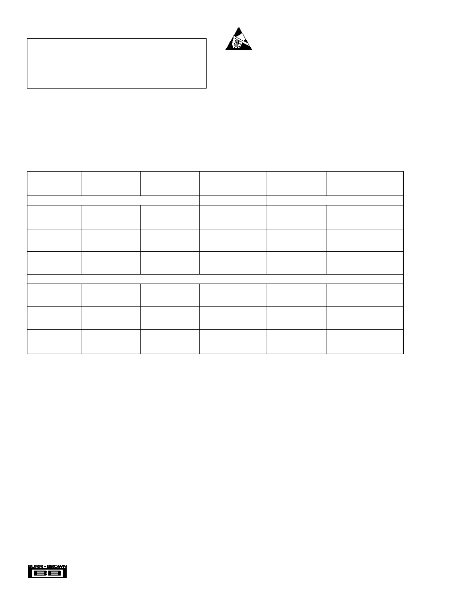
OPEN-LOOP GAIN/PHASE vs FREQUENCY
0.01
0.1
160
140
120
100
80
60
40
20
0
≠20
Voltage Gain (dB)
180
160
140
120
100
80
60
40
20
0
Phase (∞)
Frequency (Hz)
1
10
100
1k
10k
100k
G
V
S
= ±15V
V
S
= +5V
POWER SUPPLY and COMMON-MODE
REJECTION RATIO vs FREQUENCY
140
120
100
80
60
40
20
0
Power Supply Rejection Ratio (dB)
Frequency (Hz)
0.1
1
10
100
1k
10k
100k
≠PSRR
+PSRR
CMRR
V
S
=
±
15V
V
S
=
±
5V
INPUT VOLTAGE AND CURRENT
NOISE SPECTRAL DENSITY vs FREQUENCY
1k
100
10
1k
100
10
Voltage Noise (nV/
˜
Hz)
Frequency (Hz)
0.1
1
10
100
1k
10k
Current Noise (fA/
Hz)
Current Noise
Voltage Noise
CHANNEL SEPARATION vs FREQUENCY
Frequency (Hz)
Channel Separation (dB)
140
130
120
110
100
90
80
70
100
10
1k
10k
100k
Dual and quad devices.
G = 1, all channels.
Quad measured channel
A to D or B to C--other
combinations yield improved
rejection.
QUIESCENT CURRENT vs SUPPLY VOLTAGE
Total Supply Voltage (V)
Quiescent Current (
µ
A)
30
28
26
24
22
0
5
10
15
20
25
30
35
40
Per Amplifier
QUIESCENT CURRENT vs TEMPERATURE
Temperature (
∞
C)
Quiescent Current (
µ
A)
40
35
30
25
20
15
≠75
≠50
≠25
0
25
50
75
100
125
V
S
=
±
15V
V
S
= +5V
Per Amplifier
6
Æ
OPA241, 2241, 4241
OPA251, 2251, 4251
TYPICAL PERFORMANCE CURVES
(CONT)
At T
A
= +25
∞
C, and R
L
= 100k
connected to V
S
/2 (ground for V
S
=
±
15V), unless otherwise noted.
Curves apply to OPA241 and OPA251 unless specified.
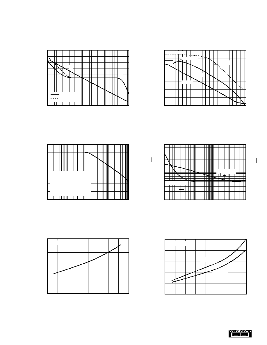
INPUT BIAS CURRENT vs TEMPERATURE
Temperature (
∞
C)
Input Bias Current (nA)
≠6
≠4
≠2
0
2
≠75
≠50
≠25
0
25
50
75
100
125
I
B
I
OS
INPUT BIAS CURRENT
vs INPUT COMMON-MODE VOLTAGE
Common-Mode Voltage (V)
Input Bias Current (nA)
≠5
≠4
≠3
≠2
≠1
0
0
5
10
15
20
25
30
I
B
I
OS
COMMON-MODE REJECTION vs TEMPERATURE
Temperature (
∞
C)
Common-Mode Rejection (dB)
140
120
100
80
60
40
20
0
≠75
≠50
≠25
0
25
50
75
100
125
V
S
=
±
15V
V
S
= +2.7V, +5V
V
CM
= (V≠) ≠0.1V to (V+) ≠0.8V
V
CM
= (V≠) ≠0.2V to (V+) ≠0.8V
V
CM
= (V≠) to (V+) ≠0.8V
SHORT-CIRCUIT CURRENT vs TEMPERATURE
Temperature (
∞
C)
Short-Circuit Current (mA)
50
45
40
35
30
25
20
15
10
5
0
≠75
≠50
≠25
0
25
50
75
100
125
≠I
SC
+I
SC
, V
S
= +5V,
±
15V (all versions)
V
S
= +5V
V
S
=
±
15V
V
S
= +5V
V
S
=
±
15V
Single Versions
Dual, Quad Versions
OUTPUT VOLTAGE SWING vs OUTPUT CURRENT
(V+)
(V+) ≠0.1V
(V+) ≠0.2V
(V+) ≠0.3V
(V≠) +0.3V
(V≠) +0.2V
(V≠) +0.1V
(V≠)
0.1
±1
±10
Output Current (mA)
Output Voltage Swing (V)
T = +125∞C
T = +25∞C
T = ≠55∞C
T = +125∞C
T = +25∞C, ≠55∞C
OPEN-LOOP GAIN AND POWER
SUPPLY REJECTION vs TEMPERATURE
Temperature (∞C)
A
OL
, PSR (dB)
140
130
120
110
100
≠75
≠50
≠25
0
25
50
75
100
125
R
L
= 20k
, 100k
R
L
= 10k
R
L
= 100k
PSRR
A
OL
, V
S
= ±15V
A
OL
, V
S
= +5V
7
Æ
OPA241, 2241, 4241
OPA251, 2251, 4251
TYPICAL PERFORMANCE CURVES
(CONT)
At T
A
= +25
∞
C, and R
L
= 100k
connected to V
S
/2 (ground for V
S
=
±
15V), unless otherwise noted.
Curves apply to OPA241 and OPA251 unless specified.
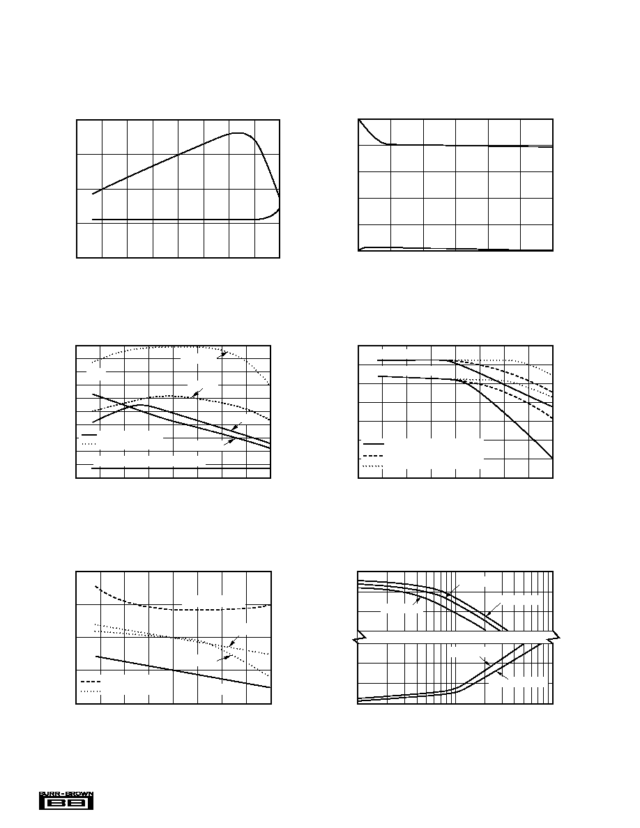
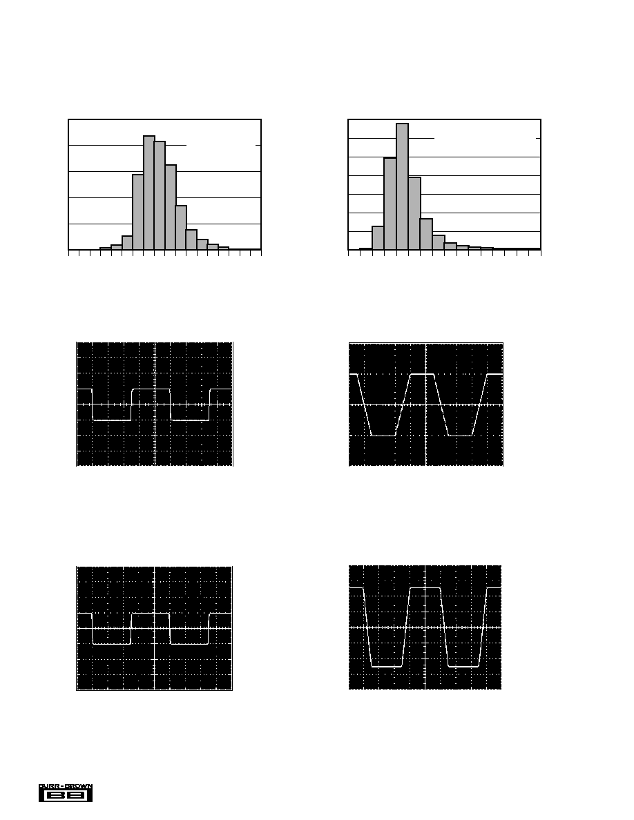
OPA251 SERIES OFFSET VOLTAGE DRIFT
PRODUCTION DISTRIBUTION
Percent of Amplifiers (%)
Offset Voltage Drift (
µ
V/
∞
C)
18
16
14
12
10
8
6
4
2
0
0
0.1
0.2
0.3
0.4
0.5
0.6
0.7
0.8
0.9
1.0
1.1
1.2
1.3
1.4
1.5
1.6
1.7
1.8
1.9
2.0
Typical production distribution
of packaged units. Singles,
duals, and quads included.
V
S
=
±
15V
OPA241 SERIES OFFSET VOLTAGE
PRODUCTION DISTRIBUTION
Percent of Amplifiers (%)
Offset Voltage (
µ
V)
30
25
20
15
10
5
0
V
S
= +5V
≠225
≠200
≠175
≠150
≠125
≠100
≠75
≠50
≠25
0
25
50
75
100
125
150
175
200
225
Typical production
distribution of
packaged units.
Singles, duals,
and quads included.
OPA241 SERIES OFFSET VOLTAGE DRIFT
PRODUCTION DISTRIBUTION
Percent of Amplifiers (%)
Offset Voltage (
µ
V/
∞
C)
20
18
16
14
12
10
8
6
4
2
0
Typical production distribution
of packaged units. Singles,
duals, and quads included.
V
S
= +5V
0
0.1 0.2 0.3 0.4 0.5 0.6 0.7 0.8 0.9 1.0 1.1 1.2 1.3
OPA251 SERIES OFFSET VOLTAGE
PRODUCTION DISTRIBUTION
Percent of Amplifiers (%)
Offset Voltage (
µ
V)
30
25
20
15
10
5
0
V
S
=
±
15V
≠225
≠200
≠175
≠150
≠125
≠100
≠75
≠50
≠25
0
25
50
75
100
125
150
175
200
225
Typical production
distribution of
packaged units.
Singles, duals,
and quads included.
MAXIMUM OUTPUT VOLTAGE vs FREQUENCY
100k
100
1k
10k
Frequency (Hz)
10
30
25
20
15
10
5
0
Maximum Output Voltage (Vp-p)
Maximum output
voltage without
slew rate-induced
distortion.
V
S
= 2.7V
V
S
= +5V
V
S
= ±15V
OPEN-LOOP GAIN vs OUTPUT VOLTAGE SWING
140
130
120
110
100
90
80
Open-Loop Gain (dB)
Output Voltage Swing from Rail (mV)
500
400
300
200
100
0
V
S
= ±15V
V
S
= +5V
V
S
= +2.7V
R
L
= 20k
R
L
= 100k
R
L
= 10k
8
Æ
OPA241, 2241, 4241
OPA251, 2251, 4251
TYPICAL PERFORMANCE CURVES
(CONT)
At T
A
= +25
∞
C, and R
L
= 100k
connected to V
S
/2 (ground for V
S
±
15V), unless otherwise noted.
Curves apply to OPA241 and OPA251 unless specified.
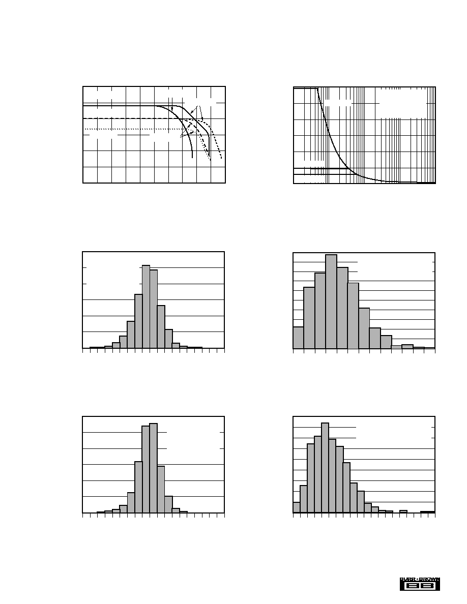
0.5V/div
OPA241
SMALL-SIGNAL STEP RESPONSE
V
S
= +5V, G = +1, R
L
= 100k
, C
L
= 100pF
OPA241
LARGE-SIGNAL STEP RESPONSE
V
S
= +5V, G + 1, R
L
= 100k
, C
L
= 100pF
OPA251
SMALL-SIGNAL STEP RESPONSE
V
S
=
±
15V, G = +1, R
L
= 100k
, C
L
= 500pF
OPA251
LARGE-SIGNAL STEP RESPONSE
V
S
=
±
15V, G = +1, R
L
= 100k
, C
L
= 500pF
50mV/div
200
µ
s/div
200
µ
s/div
2V/div
50mV/div
200
µ
s/div
2ms/div
QUIESCENT CURRENT
PRODUCTION DISTRIBUTION
Percent of Amplifiers (%)
Quiescent Current (
µ
A)
35
30
25
20
15
10
5
0
22
23
24
25
26
27
28
29
30
31
32
33
34
35
36
37
38
V
S
=
±
15V
Per Amplifier
Typical production distribution
of packaged units. Singles,
duals, and quads included.
QUIESCENT CURRENT
PRODUCT DISTRIBUTION
Percent of Amplifiers (%)
Quiescent Current (
µ
A)
25
20
15
10
5
0
21
21.5
22
22.5
23
23.5
24
24.5
25
25.5
26
26.5
27
27.5
28
28.5
29
29.5
30
V
S
= +5V
Per Amplifier
Typical production
distribution of
packaged units.
Singles, duals,
and quads included.

9
Æ
OPA241, 2241, 4241
OPA251, 2251, 4251
APPLICATIONS INFORMATION
The OPA241 and OPA251 series are unity-gain stable and
suitable for a wide range of general purpose applications.
Power supply pins should be bypassed with 0.01
µ
F ceramic
capacitors.
OPERATING VOLTAGE
The OPA241 series is laser-trimmed for low offset voltage
and drift at low supply voltage (V
S
= +5V). The OPA251
series is trimmed for
±
15V operation. Both products operate
over the full voltage range (+2.7V to +36V or
±
1.35V to
±
18V) with some compromises in offset voltage and drift
performance. However, all other parameters have similar
performance. Key parameters are guaranteed over the speci-
fied temperature range, ≠40
∞
C to +85
∞
C. Most behavior
remains unchanged throughout the full operating voltage
range. Parameters which vary significantly with operating
voltage or temperature are shown in typical performance
curves.
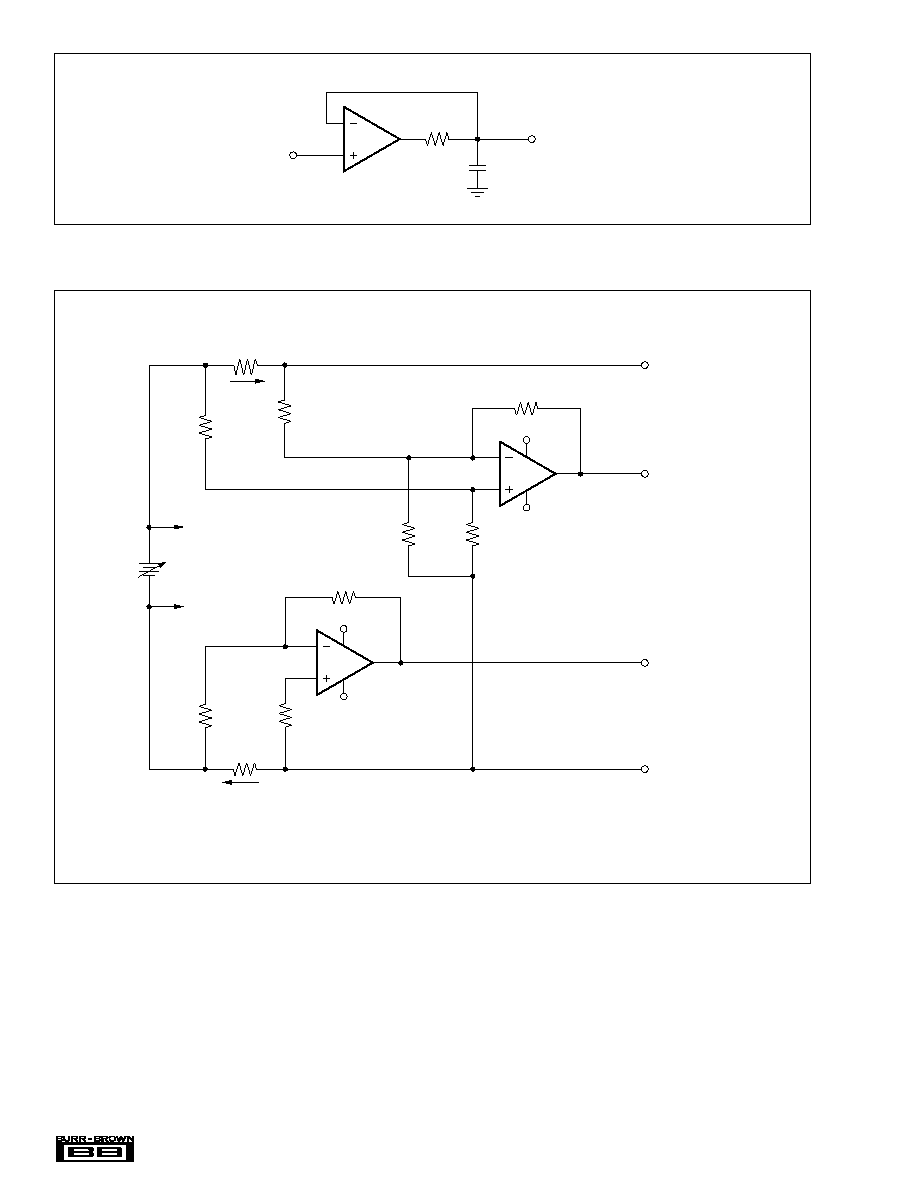
OFFSET VOLTAGE TRIM
As mentioned previously, offset voltage of the OPA241
series is laser-trimmed at +5V. The OPA251 series is trimmed
at
±
15V. Because the initial offset is so low, user adjustment
is usually not required. However, the OPA241 and OPA251
(single op amp versions) provide offset voltage trim connec-
tions on pins 1 and 5. Offset voltage can be adjusted by
connecting a potentiometer as shown in Figure 1. This
adjustment should be used only to null the offset of the op
amp, not to adjust system offset or offset produced by the
signal source. Nulling offset could degrade the offset drift
behavior of the op amp. While it is not possible to predict the
exact change in drift, the effect is usually small.
Figures 2 and 3 show the regions where the OPA241 series
and OPA251 series have the potential for instability. As
shown, the unity gain configuration with low supplies is the
most susceptible to the effects of capacitive load. With V
S
=
+5V, G = +1, and I
OUT
= 0, operation remains stable with
load capacitance up to approximately 200pF. Increasing
supply voltage, output current, and/or gain significantly
improves capacitive load drive. For example, increasing the
supplies to
±
15V and gain to 10 allows approximately
2700pF to be driven.
One method of improving capacitive load drive in the unity
gain configuration is to insert a resistor inside the feedback
loop as shown in Figure 4. This reduces ringing with large
capacitive loads while maintaining dc accuracy. For ex-
ample, with V
S
=
±
1.35V and R
S
= 5k
, the OPA241 series
and OPA251 series perform well with capacitive loads in
excess of 1000pF. Without the series resistor, capacitive
load drive is typically 200pF for these conditions. However,
this method will result in a slight reduction of output voltage
swing.
CAPACITIVE LOAD AND STABILITY
The OPA241 series and OPA251 series can drive a wide
range of capacitive loads. However, all op amps under
certain conditions may be unstable. Op amp configuration,
gain, and load value are just a few of the factors to consider
when determining stability.
V+
V≠
100k
Use offset adjust pins only to null
offset voltage of op amp--see text.
Trim Range:
±
2mV
(V≠) = 0V for single-supply operation.
OPA241
6
7
5
4
3
2
1
0.01
µ
F
0.01
µ
F
OPA241 and OPA251 (single op amps) only.
FIGURE 1. OPA241 and OPA251 Offset Voltage Trim
Circuit.
100k
10k
1k
100
Capacitive Load (pF)
Output Current (mA)
≠1
≠0.1
≠0.01
0
0.01
0.1
1
Operation above
selected gain curve
not recommended
G = 10
G = ≠1
G = +1
Sinking
Sourcing
V
S
= +2.7V
V
S
= +5V
FIGURE 2. Stability--Capacitive Load versus Output Cur-
rent for Low Supply Voltage.
FIGURE 3. Stability--Capacitive Load versus Output Cur-
rent for
±
15V Supplies.
100k
10k
1k
100
Capacitive Load (pF)
Output Current (mA)
≠1
≠0.1
≠0.01
0
0.01
0.1
1
Operation above
selected gain curve
not recommended
G = 10
G = ≠1
G = +1
V
S
=
±
15V
Sinking
Sourcing
10
Æ
OPA241, 2241, 4241
OPA251, 2251, 4251
R
L
10
A1
OPA241
+
R
1
38.3k
R
3
38.3k
R
5
383k
R
6
10k
R
7
9.09k
R
4
20k
R
2
19.1k
A2
OPA241
R
8
100k
R
H
10
I
H
V+
V≠
V+
V≠
2.7V to ±15V
V+ for A
1
, A
2
≠In
+In
≠In
+In
V
O
= 10 ∑ I
H
∑ R
H
To Load
To Load
V
O
= 10 ∑ I
L
∑ R
L
Common-mode range of A2
extends to V≠ for low-side sensing.
Optional for I
B
Cancellation
(R
7
= R
6
II R
8
)
R
2
and R
4
divide down the
common-mode input to A1.
Low-Side
Current Sense
High-Side
Current Sense
Out
Out
NOTE: Low and high-side sensing circuits can be used independently.
V≠ for A
1
, A
2
I
L
FIGURE 5. Low and High-Side Battery Current Sensing.
R
S
5k
OPA241
C
L
V
IN
V
OUT
FIGURE 4. Series Resistor in Unity Gain Configuration Improves Capacitive Load Drive.
PACKAGING INFORMATION
ORDERABLE DEVICE
STATUS(1)
PACKAGE TYPE
PACKAGE DRAWING
PINS
PACKAGE QTY
OPA2241PA
ACTIVE
PDIP
P
8
50
OPA2241UA
ACTIVE
SOIC
D
8
100
OPA2241UA/2K5
ACTIVE
SOIC
D
8
2500
OPA2251PA
ACTIVE
PDIP
P
8
50
OPA2251UA
ACTIVE
SOIC
D
8
100
OPA2251UA/2K5
ACTIVE
SOIC
D
8
2500
OPA241PA
ACTIVE
PDIP
P
8
50
OPA241UA
ACTIVE
SOIC
D
8
100
OPA241UA/2K5
ACTIVE
SOIC
D
8
2500
OPA251PA
ACTIVE
PDIP
P
8
50
OPA251UA
ACTIVE
SOIC
D
8
100
OPA251UA/2K5
ACTIVE
SOIC
D
8
2500
OPA4241PA
ACTIVE
PDIP
N
14
25
OPA4241UA
ACTIVE
SOIC
D
14
58
OPA4241UA/2K5
ACTIVE
SOIC
D
14
2500
OPA4251PA
ACTIVE
PDIP
N
14
25
OPA4251UA
ACTIVE
SOIC
D
14
58
OPA4251UA/2K5
ACTIVE
SOIC
D
14
2500
(1) The marketing status values are defined as follows:
ACTIVE: Product device recommended for new designs.
LIFEBUY: TI has announced that the device will be discontinued, and a lifetime-buy period is in effect.
NRND: Not recommended for new designs. Device is in production to support existing customers, but TI does not recommend using this part in
a new design.
PREVIEW: Device has been announced but is not in production. Samples may or may not be available.
OBSOLETE: TI has discontinued the production of the device.
PACKAGE OPTION ADDENDUM
www.ti.com
3-Oct-2003

IMPORTANT NOTICE
Texas Instruments Incorporated and its subsidiaries (TI) reserve the right to make corrections, modifications,
enhancements, improvements, and other changes to its products and services at any time and to discontinue
any product or service without notice. Customers should obtain the latest relevant information before placing
orders and should verify that such information is current and complete. All products are sold subject to TI's terms
and conditions of sale supplied at the time of order acknowledgment.
TI warrants performance of its hardware products to the specifications applicable at the time of sale in
accordance with TI's standard warranty. Testing and other quality control techniques are used to the extent TI
deems necessary to support this warranty. Except where mandated by government requirements, testing of all
parameters of each product is not necessarily performed.
TI assumes no liability for applications assistance or customer product design. Customers are responsible for
their products and applications using TI components. To minimize the risks associated with customer products
and applications, customers should provide adequate design and operating safeguards.
TI does not warrant or represent that any license, either express or implied, is granted under any TI patent right,
copyright, mask work right, or other TI intellectual property right relating to any combination, machine, or process
in which TI products or services are used. Information published by TI regarding third-party products or services
does not constitute a license from TI to use such products or services or a warranty or endorsement thereof.
Use of such information may require a license from a third party under the patents or other intellectual property
of the third party, or a license from TI under the patents or other intellectual property of TI.
Reproduction of information in TI data books or data sheets is permissible only if reproduction is without
alteration and is accompanied by all associated warranties, conditions, limitations, and notices. Reproduction
of this information with alteration is an unfair and deceptive business practice. TI is not responsible or liable for
such altered documentation.
Resale of TI products or services with statements different from or beyond the parameters stated by TI for that
product or service voids all express and any implied warranties for the associated TI product or service and
is an unfair and deceptive business practice. TI is not responsible or liable for any such statements.
Following are URLs where you can obtain information on other Texas Instruments products and application
solutions:
Products
Applications
Amplifiers
amplifier.ti.com
Audio
www.ti.com/audio
Data Converters
dataconverter.ti.com
Automotive
www.ti.com/automotive
DSP
dsp.ti.com
Broadband
www.ti.com/broadband
Interface
interface.ti.com
Digital Control
www.ti.com/digitalcontrol
Logic
logic.ti.com
Military
www.ti.com/military
Power Mgmt
power.ti.com
Optical Networking
www.ti.com/opticalnetwork
Microcontrollers
microcontroller.ti.com
Security
www.ti.com/security
Telephony
www.ti.com/telephony
Video & Imaging
www.ti.com/video
Wireless
www.ti.com/wireless
Mailing Address:
Texas Instruments
Post Office Box 655303 Dallas, Texas 75265
Copyright
2003, Texas Instruments Incorporated