1
Æ
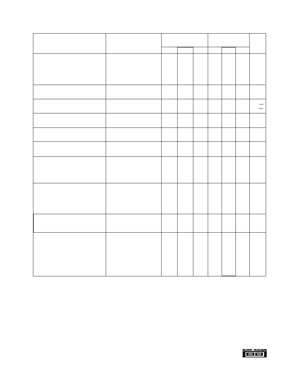
OPA234, 2234, 4234
1
2
3
4
5
6
7
14
13
12
11
10
9
8
Out D
≠In D
+In D
V≠
+In C
≠In C
Out C
Out A
≠In A
+In A
V+
+In B
≠In B
Out B
OPA4234
14-Pin DIP
SO-14
A
D
B
C
Æ
OPA234
OPA2234
OPA4234
Low Power, Precision
SINGLE-SUPPLY OPERATIONAL AMPLIFIERS
FEATURES
q
WIDE SUPPLY RANGE:
Single Supply: V
S
= +2.7V to +36V
Dual Supply: V
S
=
±
1.35V to
±
18V
q
GUARANTEED PERFORMANCE:
+2.7V, +5V, and
±
15V
q
LOW QUIESCENT CURRENT: 250
µ
A/amp
q
LOW INPUT BIAS CURRENT: 25nA max
q
LOW OFFSET VOLTAGE: 100
µ
V max
q
HIGH CMRR, PSRR, and A
OL
q
SINGLE, DUAL, and QUAD VERSIONS
DESCRIPTION
The OPA234 series low cost op amps are ideal for
single supply, low voltage, low power applications. The
series provides lower quiescent current than older
"1013"-type products and comes in current industry-
standard packages and pinouts. The combination of low
offset voltage, high common-mode rejection, high power
supply rejection, and a wide supply range provides
excellent accuracy and versatility. Single, dual, and
quad versions have identical specifications for maxi-
mum design flexibility. These general purpose op amps
are ideal for portable and battery powered applications.
OPA234 series op amps operate from either single or
dual supplies. In single supply operation, the input com-
mon-mode range extends below ground and the output
can swing to within 50mV of ground. Excellent phase
margin makes the OPA234 series ideal for demanding
applications, including high load capacitance. Dual and
quad designs feature completely independent circuitry
for lowest crosstalk and freedom from interaction.
Single version packages are DIP-8, SO-8 surface-mount,
and a space-saving MSOP-8 surface-mount. Dual pack-
ages are DIP-8 and SO-8 surface-mount. Quad pack-
ages are DIP-14 and SO-14 surface-mount. All are
specified for ≠40
∞
C to +85
∞
C operation.
1
2
3
4
8
7
6
5
V+
Out B
≠In B
+In B
Out A
≠In A
+In A
V≠
OPA2234
8-Pin DIP, SO-8
A
B
1
2
3
4
8
7
6
5
NC
V+
Output
Offset Trim
Offset Trim
≠In
+In
V≠
OPA234
8-Pin DIP, SO-8, MSOP-8
International Airport Industrial Park ∑ Mailing Address: PO Box 11400, Tucson, AZ 85734 ∑ Street Address: 6730 S. Tucson Blvd., Tucson, AZ 85706 ∑ Tel: (520) 746-1111
Twx: 910-952-1111 ∑ Internet: http://www.burr-brown.com/ ∑ Cable: BBRCORP ∑ Telex: 066-6491 ∑ FAX: (520) 889-1510 ∑ Immediate Product Info: (800) 548-6132
OPA234
OPA234
OPA2234
OPA2234
OPA4234
OPA234
OPA4234
© 1996 Burr-Brown Corporation
PDS-1318B
Printed in U.S.A., May, 2000
For most current data sheet and other product
information, visit www.burr-brown.com
SBOS055

2
Æ
OPA234, 2234, 4234
The information provided herein is believed to be reliable; however, BURR-BROWN assumes no responsibility for inaccuracies or omissions. BURR-BROWN assumes
no responsibility for the use of this information, and all use of such information shall be entirely at the user's own risk. Prices and specifications are subject to change
without notice. No patent rights or licenses to any of the circuits described herein are implied or granted to any third party. BURR-BROWN does not authorize or warrant
any BURR-BROWN product for use in life support devices and/or systems.
SPECIFICATIONS: V
S
= +5V
At T
A
= 25
∞
C, V
S
= +5V, R
L
= 10k
connected to V
S
/2 and V
OUT
= V
S
/2, unless otherwise noted.
OPA234P, U, E
OPA2234P, U
OPA234PA, UA, EA
OPA2234PA, UA
OPA4234PA, UA, U
PARAMETER
CONDITION
MIN
TYP
MAX
MIN
TYP
MAX
UNITS
OFFSET VOLTAGE
Input Offset Voltage
V
OS
V
CM
= 2.5V
±
40
±
100
T
±
250
µ
V
OPA234E, EA
±
100
±
150
T
±
350
µ
V
vs Temperature
(1)
dV
OS
/dT
Operating Temperature Range
±
0.5
±
3
T
T
µ
V/
∞
C
vs Power Supply
PSRR
V
S
= +2.7V to +30V, V
CM
= 1.7V
3
10
T
20
µ
V/V
vs Time
0.2
T
µ
V/mo
Channel Separation (Dual, Quad)
0.3
T
µ
V/V
INPUT BIAS CURRENT
Input Bias Current
(2)
I
B
V
CM
= 2.5V
≠15
≠30
T
≠50
nA
Input Offset Current
I
OS
V
CM
= 2.5V
±
1
±
5
T
T
nA
NOISE
f = 1kHz
Input Voltage Noise Density
v
n
25
T
nV/
Hz
Current Noise Density
i
n
80
T
fA/
Hz
INPUT VOLTAGE RANGE
Common-Mode Voltage Range
≠0.1
(V+) ≠1
T
T
V
Common-Mode Rejection
CMRR
V
CM
= ≠0.1V to 4V
91
106
86
T
dB
INPUT IMPEDANCE
Differential
10
7
|| 5
T
|| pF
Common-Mode
V
CM
= 2.5V
10
10
|| 6
T
|| pF
OPEN-LOOP GAIN
V
O
= 0.25V to 4V
Open-Loop Voltage Gain
A
OL
R
L
= 10k
108
120
100
T
dB
R
L
= 2k
86
96
86
T
dB
FREQUENCY RESPONSE
Gain-Bandwidth Product
GBW
C
L
= 100pF
0.35
T
MHz
Slew Rate
SR
0.2
T
V/
µ
s
Settling Time: 0.1%
G = 1, 3V Step, C
L
= 100pF
15
T
µ
s
0.01%
G = 1, 3V Step, C
L
= 100pF
25
T
µ
s
Overload Recovery Time
(V
IN
) (Gain) = V
S
16
T
µ
s
OUTPUT
Voltage Output: Positive
R
L
= 10k
to V
S
/2
(V+) ≠1
(V+) ≠0.65
T
T
V
Negative
R
L
= 10k
to V
S
/2
0.25
0.05
T
T
V
Positive
R
L
= 10k
to Ground
(V+) ≠1
(V+) ≠0.65
T
T
V
Negative
R
L
= 10k
to Ground
0.1
0.05
T
T
V
Short-Circuit Current
I
SC
±
11
T
mA
Capacitive Load Drive (Stable Operation)
(3)
G = +1
1000
T
pF
POWER SUPPLY
Specified Operating Voltage
+5
T
V
Operating Voltage Range
+2.7
+36
T
T
V
Quiescent Current (per amplifier)
I
Q
I
O
= 0
250
300
T
T
µ
A
TEMPERATURE RANGE
Specified Range
≠40
+85
T
T
∞
C
Operating Range
≠40
+125
T
T
∞
C
Storage
≠55
+125
T
T
∞
C
Thermal Resistance
JA
8-Pin DIP
100
T
∞
C/W
SO-8 Surface-Mount
150
T
∞
C/W
MSOP-8 Surface-Mount
220
T
∞
C/W
14-Pin DIP
80
T
∞
C/W
SO-14 Surface-Mount
110
T
∞
C/W
T
Specifications same as OPA234P,U,E.
NOTES: (1) Guaranteed by wafer-level test to 95% confidence level. (2) Positive conventional current flows into the input terminals. (3) See "Small-Signal Overshoot
vs Load Capacitance" typical curve.
3
Æ
OPA234, 2234, 4234
SPECIFICATIONS: V
S
= +2.7V
At T
A
= 25
∞
C, V
S
= +2.7V, R
L
= 10k
connected to V
S
/2 and V
OUT
= V
S
/2, unless otherwise noted.
OPA234P, U, E
OPA2234P, U
OPA234PA, UA, EA
OPA2234PA, UA
OPA4234PA, UA, U
PARAMETER
CONDITION
MIN
TYP
MAX
MIN
TYP
MAX
UNITS
OFFSET VOLTAGE
Input Offset Voltage
V
OS
V
CM
= 1.35V
±
40
±
100
T
±
250
µ
V
OPA234E, EA
±
100
±
150
T
±
350
µ
V
vs Temperature
(1)
dV
OS
/dT
Operating Temperature Range
±
0.5
±
3
T
T
µ
V/
∞
C
vs Power Supply
PSRR
V
S
= +2.7V to +30V, V
CM
= 1.7V
3
10
T
20
µ
V/V
vs Time
0.2
T
µ
V/mo
Channel Separation (Dual, Quad)
0.3
T
µ
V/V
INPUT BIAS CURRENT
Input Bias Current
(2)
I
B
V
CM
= 1.35V
≠15
≠30
T
≠50
nA
Input Offset Current
I
OS
V
CM
= 1.35V
±
1
±
5
T
T
n
NOISE
f = 1kHz
Input Voltage Noise Density
v
n
25
T
nV/
Hz
Current Noise Density
i
n
80
T
fA/
Hz
INPUT VOLTAGE RANGE
Common-Mode Voltage Range
≠0.1
(V+) ≠1
T
T
V
Common-Mode Rejection
CMRR
V
CM
= ≠0.1V to 1.7V
91
106
86
T
dB
INPUT IMPEDANCE
Differential
10
7
|| 5
T
|| pF
Common-Mode
V
CM
= 1.35V
10
10
|| 6
T
|| pF
OPEN-LOOP GAIN
V
O
= 0.25V to 1.7V
Open-Loop Voltage Gain
A
OL
R
L
= 10k
108
125
100
T
dB
R
L
= 2k
86
96
86
T
dB
FREQUENCY RESPONSE
Gain-Bandwidth Product
GBW
C
L
= 100pF
0.35
T
MHz
Slew Rate
SR
0.2
T
V/
µ
s
Settling Time: 0.1%
G = 1, 1V Step, C
L
= 100pF
6
T
µ
s
0.01%
G = 1, 1V Step, C
L
= 100pF
16
T
µ
s
Overload Recovery Time
(V
IN
)
(Gain) = V
S
8
T
µ
s
OUTPUT
Voltage Output: Positive
R
L
= 10k
to V
S
/2
(V+) ≠1
(V+) ≠0.6
T
T
V
Negative
R
L
= 10k
to V
S
/2
0.25
0.05
T
T
V
Positive
R
L
= 10k
to Ground
(V+) ≠1
(V+) ≠0.65
T
T
V
Negative
R
L
= 10k
to Ground
0.1
0.05
T
T
V
Short-Circuit Current
I
SC
±
8
T
mA
Capacitive Load Drive (Stable Operation)
(3)
G = +1
1000
T
pF
POWER SUPPLY
Specified Operating Voltage
+2.7
T
V
Operating Voltage Range
+2.7
+36
T
T
V
Quiescent Current (per amplifier)
I
Q
I
O
= 0
250
300
T
T
µ
A
TEMPERATURE RANGE
Specified Range
≠40
+85
T
T
∞
C
Operating Range
≠40
+125
T
T
∞
C
Storage
≠55
+125
T
T
∞
C
Thermal Resistance
JA
8-Pin DIP
100
T
∞
C/W
SO-8 Surface-Mount
150
T
∞
C/W
MSOP-8 Surface-Mount
220
T
∞
C/W
14-Pin DIP
80
T
∞
C/W
SO-14 Surface-Mount
110
T
∞
C/W
T
Specifications same as OPA234P,U,E.
NOTES: (1) Guaranteed by wafer-level test to 95% confidence level. (2) Positive conventional current flows into the input terminals. (3) See "Small-Signal Overshoot
vs Load Capacitance" typical curve.
4
Æ
OPA234, 2234, 4234
PARAMETER
CONDITION
MIN
TYP
MAX
MIN
TYP
MAX
UNITS
OFFSET VOLTAGE
Input Offset Voltage
V
OS
V
CM
= 0V
±
70
±
250
T
±
500
µ
V
OPA4234U Model
±
70
±
250
µ
V
vs Temperature
(1)
dV
OS
/dT
Operating Temperature Range
±
0.5
±
5
T
T
µ
V/
∞
C
vs Power Supply
PSRR
V
S
=
±
1.35V to
±
18V, V
CM
= 0V
3
10
T
20
µ
V/V
vs Time
0.2
T
µ
V/mo
Channel Separation (Dual, Quad)
0.3
T
µ
V/V
INPUT BIAS CURRENT
Input Bias Current
(2)
I
B
V
CM
= 0V
≠12
≠25
T
≠50
nA
Input Offset Current
I
OS
V
CM
= 0V
±
1
±
5
T
T
nA
NOISE
f = 1kHz
Input Voltage Noise Density
v
n
25
T
nV/
Hz
Current Noise Density
i
n
80
T
fA/
Hz
INPUT VOLTAGE RANGE
Common-Mode Voltage Range
(V≠)
(V+) ≠1
T
T
V
Common-Mode Rejection
CMRR
V
CM
= ≠15V to 14V
91
106
86
T
dB
INPUT IMPEDANCE
Differential
10
7
|| 5
T
|| pF
Common-Mode
V
CM
= 0V
10
10
|| 6
T
|| pF
OPEN-LOOP GAIN
Open-Loop Voltage Gain
A
OL
V
O
= ≠14.5V to 14V
110
120
100
T
dB
FREQUENCY RESPONSE
Gain-Bandwidth Product
GBW
C
L
= 100pF
0.35
T
MHz
Slew Rate
SR
0.2
T
V/
µ
s
Settling Time: 0.1%
G = 1, 10V Step, C
L
= 100pF
41
T
µ
s
0.01%
G = 1, 10V Step, C
L
= 100pF
47
T
µ
s
Overload Recovery Time
(V
IN
) (Gain) = V
S
22
T
µ
s
OUTPUT
Voltage Output: Positive
(V+) ≠1
(V+) ≠0.7
T
T
V
Negative
(V≠) +0.5 (V≠) +0.15
T
T
V
Short-Circuit Current
I
SC
±
22
T
mA
Capacitive Load Drive (Stable Operation)
(3)
G = +1
1000
T
pF
POWER SUPPLY
Specified Operating Voltage
±
15
T
V
Operating Voltage Range
±
1.35
±
18
T
T
V
Quiescent Current (per amplifier)
I
Q
I
O
= 0
±
275
±
350
T
T
µ
A
TEMPERATURE RANGE
Specified Range
≠40
+85
T
T
∞
C
Operating Range
≠40
+125
T
T
∞
C
Storage
≠55
+125
T
T
∞
C
Thermal Resistance
JA
8-Pin DIP
100
T
∞
C/W
SO-8 Surface-Mount
150
T
∞
C/W
MSOP-8 Surface-Mount
220
T
∞
C/W
14-Pin DIP
80
T
∞
C/W
SO-14 Surface-Mount
110
T
∞
C/W
T
Specifications same as OPA234P,U,E.
NOTES: (1) Guaranteed by wafer-level test to 95% confidence level. (2) Positive conventional current flows into the input terminals. (3) See "Small-Signal Overshoot
vs Load Capacitance" typical curve.
SPECIFICATIONS: V
S
=
±
15V
At T
A
= 25
∞
C, V
S
=
±
15V, R
L
= 10k
connected to ground, unless otherwise noted.
OPA234P, U, E
OPA2234P, U
OPA234PA, UA, EA
OPA2234PA, UA
OPA4234PA, UA, U

5
Æ
OPA234, 2234, 4234
ELECTROSTATIC
DISCHARGE SENSITIVITY
This integrated circuit can be damaged by ESD. Burr-Brown
recommends that all integrated circuits be handled with
appropriate precautions. Failure to observe proper handling
and installation procedures can cause damage.
ESD damage can range from subtle performance degrada-
tion to complete device failure. Precision integrated circuits
may be more susceptible to damage because very small
parametric changes could cause the device not to meet its
published specifications.
ABSOLUTE MAXIMUM RATINGS
Supply Voltage, V+ to V≠ .................................................................... 36V
Input Voltage ..................................................... (V≠) ≠0.7V to (V+) +0.7V
Output Short-Circuit
(1)
.............................................................. Continuous
Operating Temperature .................................................. ≠40
∞
C to +125
∞
C
Storage Temperature ..................................................... ≠55
∞
C to +125
∞
C
Junction Temperature ...................................................................... 150
∞
C
Lead Temperature (soldering, 10s) ................................................. 300
∞
C
NOTE: (1) Short-circuit to ground, one amplifier per package.
PACKAGE
SPECIFIED
DRAWING
TEMPERATURE
PACKAGE
ORDERING
TRANSPORT
PRODUCT
PACKAGE
NUMBER
RANGE
MARKING
NUMBER
(1)
MEDIA
Single
OPA234EA
MSOP-8 Surface-Mount
337
≠40
∞
C to +85
∞
C
A34
(2)
OPA234EA/250
Tape and Reel
"
"
"
"
"
OPA234EA/2K5
Tape and Reel
OPA234E
MSOP-8 Surface-Mount
337
≠40
∞
C to +85
∞
C
A34
(2)
OPA234E/250
Tape and Reel
"
"
"
"
"
OPA234E/2K5
Tape and Reel
OPA234PA
Plastic DIP-8
006
≠40
∞
C to +85
∞
C
OPA234PA
OPA234PA
Rails
OPA234P
"
"
"
OPA234P
OPA234P
Rails
OPA234UA
SO-8 Surface-Mount
182
≠40
∞
C to +85
∞
C
OPA234UA
OPA234UA
Rails
OPA234U
"
"
"
OPA234U
OPA234U
Rails
Dual
OPA2234PA
Plastic DIP-8
006
≠40
∞
C to +85
∞
C
OPA2234PA
OPA2234PA
Rails
OPA2234P
"
"
"
OPA2234P
OPA2234P
Rails
OPA2234UA
SO-8 Surface-Mount
182
≠40
∞
C to +85
∞
C
OPA2234UA
OPA2234UA
Rails
OPA2234U
"
"
"
OPA2234U
OPA2234U
Rails
Quad
OPA4234PA
Plastic DIP-8
006
≠40
∞
C to +85
∞
C
OPA4234PA
OPA4234PA
Rails
OPA4234P
"
"
"
OPA4234P
OPA4234P
Rails
OPA4234UA
SO-8 Surface-Mount
182
≠40
∞
C to +85
∞
C
OPA4234UA
OPA4234UA
Rails
OPA4234U
"
"
"
OPA4234U
OPA4234U
Rails
NOTE: (1) Models with a slash (/) are available only in Tape and Reel in the quantities indicated (e.g., /2K5 indicates 2500 devices per reel). Ordering 2500 pieces
of "OPA234E//2K5" will get a single 2500-piece Tape and Reel. (2) The grade will be marked on the Reel.
PACKAGE/ORDERING INFORMATION

6
Æ
OPA234, 2234, 4234
INPUT NOISE AND CURRENT NOISE
SPECTRAL DENSITY vs FREQUENCY
1
1k
100
10
Voltage Noise (nV/
Hz)
Current Noise (fA/
Hz)
Frequency (Hz)
10
100
1k
10k
100k
Current Noise
Voltage Noise
TYPICAL PERFORMANCE CURVES
At T
A
= +25
∞
C and R
L
= 10k
unless otherwise noted.
INPUT BIAS CURRENT
vs INPUT COMMON-MODE VOLTAGE
Common-Mode Voltage (V)
Input Bias Current (nA)
≠17
≠16
≠15
≠14
≠13
≠12
≠11
≠10
≠15
≠10
≠5
0
5
10
15
V
S
= +5V
V
S
= +2.7V
V
S
= ±15V
INPUT BIAS AND INPUT OFFSET CURRENT
vs TEMPERATURE
Ambient Temperature (∞C)
Input Bias, Input Offset Current (nA)
≠20
≠15
≠10
≠5
0
+5
≠75
≠50
≠25
0
25
50
75
100
125
V
S
= +2.7V, +5V
I
OS
V
S
= ±15V
I
B
OPEN-LOOP GAIN/PHASE vs FREQUENCY
0.1
140
120
100
80
60
40
20
0
≠20
0
≠30
≠60
≠90
≠120
≠150
≠180
Voltage Gain (dB)
Phase (∞)
Frequency (Hz)
1
10
100
1k
10k
100k
1M
C
L
= 100pF
G
V
O
= 0.25V
V
S
= +5V
±15V
V
O
=
V
S
2
V
S
= +2.7V
CMR
+PSR
POWER SUPPLY AND COMMON-MODE REJECTION
vs FREQUENCY
Frequency (Hz)
PSR, CMR (dB)
120
110
100
90
80
70
60
50
40
30
20
10
0
10
100
1k
10k
100k
1M
≠PSR
V
S
= +2.7V, +5V
or ±15V
V
S
= +2.7V or +5V
V
S
= ±15V
CHANNEL SEPARATION vs FREQUENCY
Frequency (Hz)
Channel Separation (dB)
160
140
120
100
80
10
100
1k
10k
100k
Dual and quad devices.
G = 1, all channels.
Quad measured channel
A to D or B to C--other
combinations yield improved
rejection.
R
L
= 10k
7
Æ
OPA234, 2234, 4234
TYPICAL PERFORMANCE CURVES
(Cont.)
At T
A
= +25
∞
C and R
L
= 10k
unless otherwise noted.
OFFSET VOLTAGE
PRODUCTION DISTRIBUTION
Percent of Amplifiers (%)
Offset Voltage (µV)
0
25
25
50
75
125
100
150
175
0.3%
0.1%
200
200
175
150
125
100
75
50
25
20
15
10
5
0
V
S
= +2.7V, +5V
Typical production
distribution of packaged
units. Single, dual, and
quad units included.
0.1%
OFFSET VOLTAGE
PRODUCTION DISTRIBUTION
Percent of Amplifiers (%)
Offset Voltage (µV)
0
100
200
300
400
500
≠500
≠400
≠300
≠200
≠100
30
25
20
15
10
5
0
V
S
= ±15V
Typical production
distribution of packaged
units. Single, dual,
and quad units included.
0.2%
0.3%
0.7%
0.1%
0.5%
OFFSET VOLTAGE DRIFT
PRODUCTION DISTRIBUTION
Percent of Amplifiers (%)
Offset Voltage Drift (µV/∞C)
3
3.5
4
4.5
5
0.5
1
1.5
2
2.5
35
30
25
20
15
10
5
0
0.1%
0.1%
0.2%
0.5%
0.3%
V
S
= +5V
Typical production
distribution of packaged
units. Single, dual,
and quad units included.
OFFSET VOLTAGE DRIFT
PRODUCTION DISTRIBUTION
Percent of Amplifiers (%)
Offset Voltage Drift (µV/∞C)
30
25
20
15
10
5
0
0.5
1.5
2
1
3
3.5
2.5
4
4.5
5
5.5
6
6.5
7
8
7.5
V
S
= ±15V
Typical production
distribution of packaged
units. Single, dual,
and quad units included.
0.1%
0.1%
0.1%
0.1%
0.2%
0.4% 0.3%
OFFSET VOLTAGE DRIFT
PRODUCTION DISTRIBUTION
Percent of Amplifiers (%)
Offset Voltage Drift (µV/∞C)
3
3.5
4
4.5
5
0.5
1
1.5
2
2.5
35
30
25
20
15
10
5
0
0.1%
0.1%
0.2%
0.1%
0.3%
V
S
= +2.7V
Typical production
distribution of packaged
units. Single, dual,
and quad units included.
A
OL
, CMR, PSR vs TEMPERATURE
Ambient Temperature (∞C)
A
OL
, CMR, PSR (dB)
140
130
120
110
100
90
80
70
60
≠75
≠50
≠25
0
25
50
75
100
125
CMR
PSR
V
CM
= (V≠) ≠0.02V to (V+) ≠1V
A
OL
V
S
= +2.7V
V
S
= +5V
V
S
= ±15V
8
Æ
OPA234, 2234, 4234
TYPICAL PERFORMANCE CURVES
(Cont.)
At T
A
= +25
∞
C and R
L
= 10k
unless otherwise noted.
LARGE-SIGNAL STEP RESPONSE
G = 1, C
L
= 100pF, V
S
= +5V
1V/div
10µs/div
SMALL-SIGNAL STEP RESPONSE
G = 1, C
L
= 10,000pF, V
S
= +5V
20mV/div
20µs/div
OUTPUT VOLTAGE SWING vs OUTPUT CURRENT
V+
(V+) ≠0.5
(V+) ≠1
(V+) ≠1.5
(V+) ≠2
(V+) ≠2.5
(V+) ≠3
(V≠) +3
(V≠) +2.5
(V≠) +2
(V≠) +1.5
(V≠) +1
(V≠) +0.5
V≠
0
±5
±10
125∞C
85∞C
25∞C
±15
Output Current (mA)
Output Voltage Swing (V)
≠55∞C
≠55∞C
≠40∞C
25∞C
85∞C
125∞C
≠40∞C
High output current may
not be available at low
supply voltages due to
output swing limitations.
SMALL-SIGNAL OVERSHOOT
vs LOAD CAPACITANCE
70
60
50
40
30
20
10
0
10pF
100pF
1nF
10nF
100nF
Load Capacitance
Overshoot (%)
G = ≠1,
G = +2
G = +1,
V
S
= +2.7, +5V
G = +1,
V
S
= ±15V
G = ±10
G = ≠2
V
O
= 100mVp-p
SMALL-SIGNAL STEP RESPONSE
G = 1, C
L
= 100pF, V
S
= +5V
2µs/div
20mV/div
SETTLING TIME vs CLOSED-LOOP GAIN
Gain (V/V)
Settling Time (µs)
1000
100
10
1
±1
±10
±100
V
S
= ±15V,
10V Step
V
S
= +2.7V,
1V Step
C
L
= 100pF
0.1%
0.01%
V
S
= +5V,
3V Step

9
Æ
OPA234, 2234, 4234
QUIESCENT CURRENT AND SHORT-CIRCUIT CURRENT
vs TEMPERATURE
Temperature (∞C)
Quiescent Current (µA)
525
450
375
300
225
150
75
0
Short-Circuit Current (mA)
70
60
50
40
30
20
10
0
≠75
≠50
≠25
0
25
50
75
100
125
±I
SC
±I
Q
V
S
= +2.7V
V
S
= +5V
V
S
= +2.7V or +5V
V
S
= ±15V
APPLICATIONS INFORMATION
OPA234 series op amps are unity-gain stable and suitable
for a wide range of general-purpose applications. Power
supply pins should be bypassed with 10nF ceramic capaci-
tors.
OPERATING VOLTAGE
OPA234 series op amps operate from single (+2.7V to
+36V) or dual (
±
1.35V to
±
18V) supplies with excellent
performance. Specifications are production tested with
+2.7V, +5V, and
±
15V supplies. Most behavior remains
unchanged throughout the full operating voltage range.
Parameters which vary significantly with operating volt-
age are shown in typical performance curves.
OFFSET VOLTAGE TRIM
Offset voltage of OPA234 series amplifiers is laser trimmed
and usually requires no user adjustment. The OPA234
(single op amp version) provides offset voltage trim con-
nections on pins 1 and 5. Offset voltage can be adjusted by
connecting a potentiometer as shown in Figure 1. This
adjustment should be used only to null the offset of the op
amp, not to adjust system offset or offset produced by the
signal source. Nulling offset could degrade the offset drift
behavior of the op amp. While it is not possible to predict
the exact change in drift, the effect is usually small.
FIGURE 1. OPA234 Offset Voltage Trim Circuit.
V+
V≠
100k
OPA234 single op amp only.
Use offset adjust pins only to null
offset voltage of op amp--see text.
Trim Range: ±4mV typ
(V≠) = 0V for single supply operation.
OPA234
6
7
5
4
3
2
1
10nF
10nF
TYPICAL PERFORMANCE CURVES
(Cont.)
At T
A
= +25
∞
C and R
L
= 10k
unless otherwise noted.
MAXIMUM OUTPUT VOLTAGE
vs FREQUENCY
100k
Frequency (Hz)
1k
10k
30
25
20
15
10
5
0
Output Voltage (Vp-p)
V
S
= ±2.7V
V
S
= +5V
Maximum output voltage
without slew-rate induced
distortion
V
S
= ±15V
PACKAGING INFORMATION
ORDERABLE DEVICE
STATUS(1)
PACKAGE TYPE
PACKAGE DRAWING
PINS
PACKAGE QTY
OPA2234P
OBSOLETE
PDIP
P
8
OPA2234PA
OBSOLETE
PDIP
P
8
OPA2234U
ACTIVE
SOIC
D
8
100
OPA2234U/2K5
ACTIVE
SOIC
D
8
2500
OPA2234UA
ACTIVE
SOIC
D
8
100
OPA2234UA/2K5
ACTIVE
SOIC
D
8
2500
OPA234E/250
ACTIVE
VSSOP
DGK
8
250
OPA234E/2K5
ACTIVE
VSSOP
DGK
8
2500
OPA234EA/250
ACTIVE
VSSOP
DGK
8
250
OPA234EA/2K5
ACTIVE
VSSOP
DGK
8
2500
OPA234P
OBSOLETE
PDIP
P
8
OPA234PA
OBSOLETE
PDIP
P
8
OPA234U
ACTIVE
SOIC
D
8
100
OPA234U/2K5
ACTIVE
SOIC
D
8
2500
OPA234UA
ACTIVE
SOIC
D
8
100
OPA234UA/2K5
ACTIVE
SOIC
D
8
2500
OPA4234PA
OBSOLETE
PDIP
N
14
OPA4234U
ACTIVE
SOIC
D
14
58
OPA4234U/2K5
ACTIVE
SOIC
D
14
2500
OPA4234UA
ACTIVE
SOIC
D
14
58
OPA4234UA/2K5
ACTIVE
SOIC
D
14
2500
(1) The marketing status values are defined as follows:
ACTIVE: Product device recommended for new designs.
LIFEBUY: TI has announced that the device will be discontinued, and a lifetime-buy period is in effect.
NRND: Not recommended for new designs. Device is in production to support existing customers, but TI does not recommend using this part in
a new design.
PREVIEW: Device has been announced but is not in production. Samples may or may not be available.
OBSOLETE: TI has discontinued the production of the device.
PACKAGE OPTION ADDENDUM
www.ti.com
3-Oct-2003

IMPORTANT NOTICE
Texas Instruments Incorporated and its subsidiaries (TI) reserve the right to make corrections, modifications,
enhancements, improvements, and other changes to its products and services at any time and to discontinue
any product or service without notice. Customers should obtain the latest relevant information before placing
orders and should verify that such information is current and complete. All products are sold subject to TI's terms
and conditions of sale supplied at the time of order acknowledgment.
TI warrants performance of its hardware products to the specifications applicable at the time of sale in
accordance with TI's standard warranty. Testing and other quality control techniques are used to the extent TI
deems necessary to support this warranty. Except where mandated by government requirements, testing of all
parameters of each product is not necessarily performed.
TI assumes no liability for applications assistance or customer product design. Customers are responsible for
their products and applications using TI components. To minimize the risks associated with customer products
and applications, customers should provide adequate design and operating safeguards.
TI does not warrant or represent that any license, either express or implied, is granted under any TI patent right,
copyright, mask work right, or other TI intellectual property right relating to any combination, machine, or process
in which TI products or services are used. Information published by TI regarding third-party products or services
does not constitute a license from TI to use such products or services or a warranty or endorsement thereof.
Use of such information may require a license from a third party under the patents or other intellectual property
of the third party, or a license from TI under the patents or other intellectual property of TI.
Reproduction of information in TI data books or data sheets is permissible only if reproduction is without
alteration and is accompanied by all associated warranties, conditions, limitations, and notices. Reproduction
of this information with alteration is an unfair and deceptive business practice. TI is not responsible or liable for
such altered documentation.
Resale of TI products or services with statements different from or beyond the parameters stated by TI for that
product or service voids all express and any implied warranties for the associated TI product or service and
is an unfair and deceptive business practice. TI is not responsible or liable for any such statements.
Following are URLs where you can obtain information on other Texas Instruments products and application
solutions:
Products
Applications
Amplifiers
amplifier.ti.com
Audio
www.ti.com/audio
Data Converters
dataconverter.ti.com
Automotive
www.ti.com/automotive
DSP
dsp.ti.com
Broadband
www.ti.com/broadband
Interface
interface.ti.com
Digital Control
www.ti.com/digitalcontrol
Logic
logic.ti.com
Military
www.ti.com/military
Power Mgmt
power.ti.com
Optical Networking
www.ti.com/opticalnetwork
Microcontrollers
microcontroller.ti.com
Security
www.ti.com/security
Telephony
www.ti.com/telephony
Video & Imaging
www.ti.com/video
Wireless
www.ti.com/wireless
Mailing Address:
Texas Instruments
Post Office Box 655303 Dallas, Texas 75265
Copyright
2003, Texas Instruments Incorporated