PRODUCT
FEATURES
OPA355
200MHz GBW CMOS, 2.5V to 5V Supply
OPA354
100MHz GBW CMOS, RRIO, 2.5V to 5V Supply
OPA350
500
µ
V V
OS
, 38MHz, 2.5V to 5V Supply
OPA335
10
µ
V V
OS
, Zero-Drift, 2.5V to 5V Supply
OPA132
16MHz GBW, Precision FET Op Amp,
±
15V
OPA656/7
230MHz, Precision FET,
±
5V
LOG112
LOG amp, 7.5 decades,
±
4.5V to
±
18V Supply
LOG114
LOG amp, 7.5 decades,
±
2.25V to
±
5.5V Supply
IVC102
Precision Switched Integrator TIA
APPLICATIONS
q
PRECISION I/V CONVERSION
q
PHOTODIODE MONITORING
q
OPTICAL AMPLIFIERS
q
CAT-SCANNER FRONTEND
Precision, High-Speed
Transimpedance Amplifier
FEATURES
q
OVER 1MHz TIA BANDWIDTH
q
DYNAMIC RANGE: 5 Decades
q
EXCELLENT LONG-TERM STABILITY
q
VERY LOW 1/f NOISE
q
BIAS CURRENT: 50pA (max)
q
OFFSET VOLTAGE: 25
µ
V (max)
q
DRIFT: 0.1
µ
V/
∞
C
q
GAIN BANDWIDTH: 85MHz
q
QUIESCENT CURRENT: 6mA
q
SUPPLY RANGE: 2.7V to 5.5V
q
SINGLE AND DUAL VERSIONS
q
MicroSIZE
PACKAGE: MSOP-8
OPA380
OPA2380
SBOS291 ≠ NOVEMBER 2003
Copyright © 2003, Texas Instruments Incorporated
www.ti.com
Please be aware that an important notice concerning availability, standard warranty, and use in critical applications of
Texas Instruments semiconductor products and disclaimers thereto appears at the end of this data sheet.
All trademarks are the property of their respective owners.
OPA380 RELATED PRODUCTS
DESCRIPTION
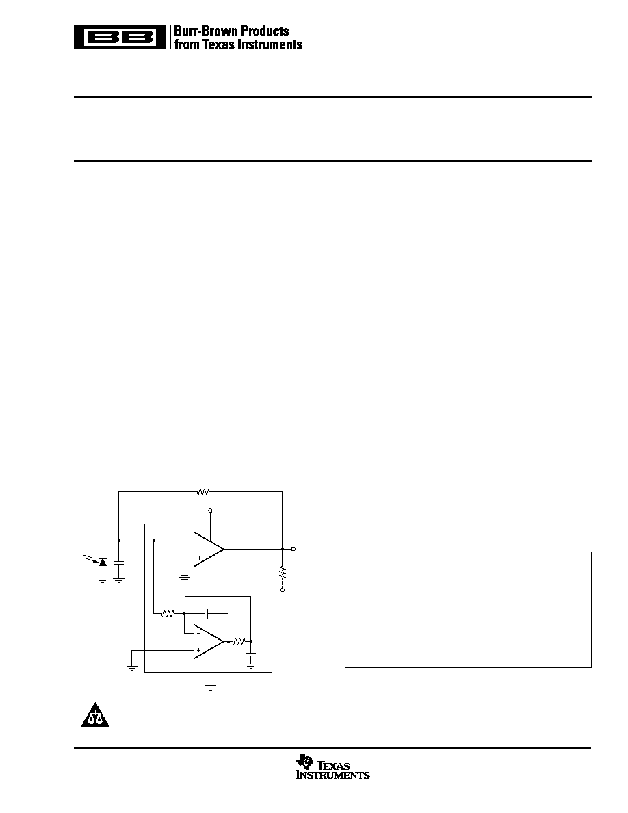
The OPA380 family of transimpedance amplifiers provides
high-speed (85MHz Gain Bandwidth (GBW)) operation, with
extremely high precision, excellent long-term stability, and
very low 1/f noise. The OPA380 features an offset voltage of
25
µ
V, offset drift of 0.1
µ
V/
∞
C, and maximum bias current of
50pA. The OPA380 far exceeds the offset, drift, and noise
performance that conventional JFET op amps provide.
The signal bandwidth of a transimpedance amplifier depends
largely on the GBW of the amplifier, and the parasitic capaci-
tance of the photodiode as well as the feedback resistor. The
85MHz GBW of the OPA380 enables a transimpedance
bandwidth of > 1MHz in most configurations. Therefore, the
OPA380 is ideally suited for fast control loops that detect and
react to fast changes in the optical power level on a fiber.
Due to the high precision and low-noise characteristics of the
OPA380, a dynamic range of 5 decades can be achieved.
This allows the measurement of signal currents in the order
of 10nA, and up to 1mA in a single I/V conversion stage. In
contrast to logarithmic amplifiers, the OPA380 provides very-
wide bandwidth, even at 10nA input currents. By using an
external pulldown resistor to ≠5V, the output voltage range
can be extended to include 0V.
The OPA380 (single) is available in MSOP-8 and SO-8
packages. The OPA2380 (dual) comes in the miniature
MSOP-8 package. They are specified from ≠40
∞
C to +125
∞
C.
PRODUCT PREVIEW information concerns products in the formative or
design phase of development. Characteristic data and other
specifications are design goals. Texas Instruments reserves the right to
change or discontinue these products without notice.
PRODUCT PREVIEW
1M
R
F
100k
+5V
7
2
3
4
6
OPA380
67pF
20mV
≠
+
75pF
C
DIODE
≠5V
R
P
(Optional
Pulldown
Resistor)
V
O
0V to 4.9V
Photodiode

2
www.ti.com
OPA380, OPA2380
SBOS291
PRODUCT PREVIEW
SPECIFIED
PACKAGE
TEMPERATURE
PACKAGE
ORDERING
TRANSPORT
PRODUCT
PACKAGE-LEAD
DESIGNATOR
(1)
RANGE
MARKING
NUMBER
MEDIA, QUANTITY
OPA380
MSOP-8
DGK
≠40
∞
C to +125
∞
C
TBD
OPA380AIDGKT
Tape and Reel, 250
"
"
"
"
"
OPA380AIDGKR
Tape and Reel, 2500
OPA380
SO-8
D
≠40
∞
C to +125
∞
C
OPA380A
OPA380AID
Rails, 100
"
"
"
"
"
OPA380AIDR
Tape and Reel, 2500
OPA2380
MSOP-8
DGK
≠40
∞
C to +125
∞
C
TBD
OPA2380AIDGKT
Rails, 250
"
"
"
"
"
OPA2380AIDGKR
Tape and Reel, 2500
Supply Voltage .................................................................................... +7V
Signal Input Terminals, Voltage
(2)
........................... ≠0.5V to (V+) + 0.5V
Current
(2)
..................................................
±
10mA
Output Short Circuit
(3)
.............................................................. Continuous
Operating Temperature .................................................. ≠40
∞
C to +125
∞
C
Storage Temperature ..................................................... ≠65
∞
C to +150
∞
C
Junction Temperature .................................................................... +150
∞
C
Lead Temperature (soldering, 10s) ............................................... +300
∞
C
NOTES: (1) Stresses above these ratings may cause permanent damage.
Exposure to absolute maximum conditions for extended periods may de-
grade device reliability. These are stress ratings only, and functional opera-
tion of the device at these, or any other conditions beyond those specified,
is not implied. (2) Input terminals are diode-clamped to the power-supply
rails. Input signals that can swing more than 0.5V beyond the supply rails
should be current-limited to 10mA or less. (3) Short-circuit to ground, one
amplifier per package.
ABSOLUTE MAXIMUM RATINGS
(1)
PACKAGE/ORDERING INFORMATION
ELECTROSTATIC
DISCHARGE SENSITIVITY
This integrated circuit can be damaged by ESD. Texas
Instruments recommends that all integrated circuits be handled
with appropriate precautions. Failure to observe proper han-
dling and installation procedures can cause damage.
ESD damage can range from subtle performance degrada-
tion to complete device failure. Precision integrated circuits
may be more susceptible to damage because very small
parametric changes could cause the device not to meet its
published specifications.
PIN CONFIGURATIONS
1
2
3
4
8
7
6
5
NC
(1)
V+
Out
NC
(1)
NC
(1)
≠In
+In
V≠
OPA380
MSOP-8, SO-8
NOTE: (1) NC indicates no internal connection.
1
2
3
4
8
7
6
5
V+
Out B
≠In B
+In B
Out A
≠In A
+In A
V≠
OPA2380
MSOP-8
Top View
3
www.ti.com
OPA380, OPA2380
SBOS291
PRODUCT PREVIEW
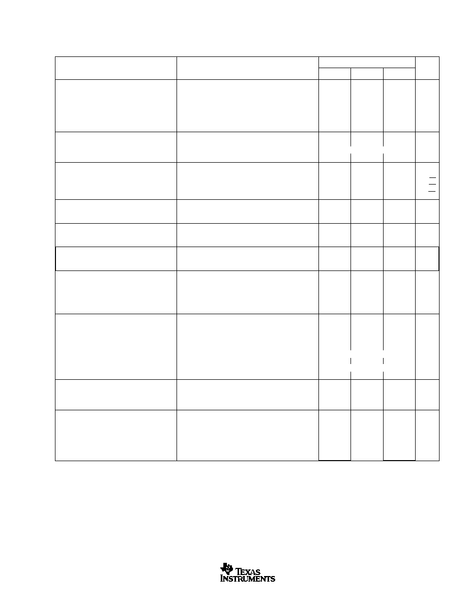
OPA380, OPA2380
ELECTRICAL CHARACTERISTICS: V
S
= +2.7V to +5.5V
Boldface limits apply over the specified temperature range, T
A
= ≠40
∞
C to +125
∞
C.
At T
A
= +25
∞
C, R
L
=2k
connected to V
S
/2, and V
OUT
= V
S
/2, unless otherwise noted.
PARAMETER
CONDITION
MIN
TYP
MAX
UNITS
OFFSET VOLTAGE
Input Offset Voltage
V
OS
V
S
= +5V, V
CM
= 0V
4
25
µ
V
Drift
dV
OS
/dT
TBD
0.1
µ
V/
∞
C
vs Power Supply
PSRR
V
S
= +2.7V to +5.5V, V
CM
= 0
2.4
10
µ
V/V
Over Temperature
V
S
= +2.7V to +5.5V, V
CM
= 0
5
µ
V/V
Long-Term Stability
(1)
See Note (1)
Channel Separation, dc
1
µ
V/V
INPUT BIAS CURRENT
Input Bias Current
I
B
V
CM
= V
S
/2
1
±
50
pA
Over Temperature
Typical Characteristics
Input Offset Current
I
OS
1
±
100
pA
NOISE
Input Voltage Noise, f = 0.1Hz to 10Hz
e
n
V
S
= +5V, V
CM
= 0V
3
µ
V
PP
Input Voltage Noise Density, f = 10kHz
e
n
V
S
= +5V, V
CM
= 0V
67
nV/
Hz
Input Voltage Noise Density, f = 1MHz
e
n
V
S
= +5V, V
CM
= 0V
5.5
nV/
Hz
Input Current Noise Density, f = 1kHz
i
n
V
S
= +5V, V
CM
= 0V
100
fA/
Hz
INPUT VOLTAGE RANGE
Common-Mode Voltage Range
V
CM
V≠
(V+) ≠ 1.8V
V
Common-Mode Rejection Ratio
CMRR
(V≠) < V
CM
< (V+) ≠ 1.8V
100
130
dB
INPUT IMPEDANCE
Differential Capacitance
1
pF
Common-Mode Resistance and Capacitance
10
13
|| 3
|| pF
OPEN-LOOP GAIN
Open-Loop Voltage Gain
A
OL
0.1V < V
O
< (V+) ≠ 0.6V, V
CM
= V
S
/2
110
130
dB
0V < V
O
< (V+) ≠ 0.6V, V
CM
= 0V,
R
P
= 2k
to ≠5V
(2)
106
120
dB
FREQUENCY RESPONSE
C
L
= 50pF
Gain-Bandwidth Product
GBW
85
MHz
Slew Rate
SR
G = +1
80
V/
µ
s
Settling Time, 0.01%
(3)
t
S
V
S
= +5.5V, 4V Step, G = +1
3.5
ns
0.0015%
(3)
V
S
= +5.5V, 4V Step, G = +1
9.2
µ
s
Overload Recovery Time
(4), (5)
V
IN
∑ G > V
S
0.5
µ
s
OUTPUT
Voltage Output Swing from Positive Rail
R
L
= 2k
10
600
mV
Voltage Output Swing from Negative Rail
R
L
= 2k
60
100
mV
Voltage Output Swing from Positive Rail
R
P
= 2k
to ≠5V
(2)
600
mV
Voltage Output Swing from Negative Rail
R
P
= 2k
to ≠5V
(2)
0
mV
Output Current
I
OUT
See Typical Characteristics
Short-Circuit Current
I
SC
200
mA
Capacitive Load Drive
C
LOAD
See Typical Characteristics
Open-Loop Output (Impedance)
f = 1MHz, I
O
= 0
TBD
POWER SUPPLY
Specified Voltage Range
V
S
2.7
5.5
V
Quiescent Current (per Amplifier)
I
Q
I
O
= 0
6
7.5
mA
Over Temperature
8
mA
TEMPERATURE RANGE
Specified Range
≠40
+125
∞
C
Operating Range
≠40
+125
∞
C
Storage Range
≠65
+150
∞
C
Thermal Resistance
JA
MSOP-8
150
∞
C/W
SO-8
150
∞
C/W
NOTES: (1) 300-hour life test at 150
∞
C demonstrated randomly distributed variation approximately equal to measurement repeatability of 1
µ
V.
(2) Tested with output connected only to R
P
, a pulldown resistor connected between V
OUT
and ≠5V, as in Figure xxx. See also applications section
Achieving Output Swing to the Negative Rail.
(3) Transimpedance frequency of 200kHz.
(4) Time required to return to linear operation.
(5) From positive rail.
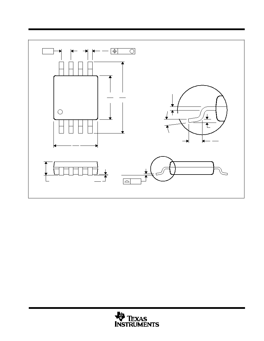
MECHANICAL DATA
MPDS028B ≠ JUNE 1997 ≠ REVISED SEPTEMBER 2001
POST OFFICE BOX 655303
∑
DALLAS, TEXAS 75265
DGK (R-PDSO-G8)
PLASTIC SMALL-OUTLINE PACKAGE
0,69
0,41
0,25
0,15 NOM
Gage Plane
4073329/C 08/01
4,98
0,25
5
3,05
4,78
2,95
8
4
3,05
2,95
1
0,38
1,07 MAX
Seating Plane
0,65
M
0,08
0
∞
≠ 6
∞
0,10
0,15
0,05
NOTES: A. All linear dimensions are in millimeters.
B. This drawing is subject to change without notice.
C. Body dimensions do not include mold flash or protrusion.
D. Falls within JEDEC MO-187
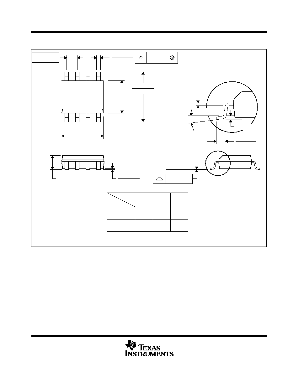
MECHANICAL DATA
MSOI002B ≠ JANUARY 1995 ≠ REVISED SEPTEMBER 2001
POST OFFICE BOX 655303
∑
DALLAS, TEXAS 75265
D (R-PDSO-G**)
PLASTIC SMALL-OUTLINE PACKAGE
8 PINS SHOWN
8
0.197
(5,00)
A MAX
A MIN
(4,80)
0.189
0.337
(8,55)
(8,75)
0.344
14
0.386
(9,80)
(10,00)
0.394
16
DIM
PINS **
4040047/E 09/01
0.069 (1,75) MAX
Seating Plane
0.004 (0,10)
0.010 (0,25)
0.010 (0,25)
0.016 (0,40)
0.044 (1,12)
0.244 (6,20)
0.228 (5,80)
0.020 (0,51)
0.014 (0,35)
1
4
8
5
0.150 (3,81)
0.157 (4,00)
0.008 (0,20) NOM
0
∞
≠ 8
∞
Gage Plane
A
0.004 (0,10)
0.010 (0,25)
0.050 (1,27)
NOTES: A. All linear dimensions are in inches (millimeters).
B. This drawing is subject to change without notice.
C. Body dimensions do not include mold flash or protrusion, not to exceed 0.006 (0,15).
D. Falls within JEDEC MS-012

IMPORTANT NOTICE
Texas Instruments Incorporated and its subsidiaries (TI) reserve the right to make corrections, modifications,
enhancements, improvements, and other changes to its products and services at any time and to discontinue
any product or service without notice. Customers should obtain the latest relevant information before placing
orders and should verify that such information is current and complete. All products are sold subject to TI's terms
and conditions of sale supplied at the time of order acknowledgment.
TI warrants performance of its hardware products to the specifications applicable at the time of sale in
accordance with TI's standard warranty. Testing and other quality control techniques are used to the extent TI
deems necessary to support this warranty. Except where mandated by government requirements, testing of all
parameters of each product is not necessarily performed.
TI assumes no liability for applications assistance or customer product design. Customers are responsible for
their products and applications using TI components. To minimize the risks associated with customer products
and applications, customers should provide adequate design and operating safeguards.
TI does not warrant or represent that any license, either express or implied, is granted under any TI patent right,
copyright, mask work right, or other TI intellectual property right relating to any combination, machine, or process
in which TI products or services are used. Information published by TI regarding third-party products or services
does not constitute a license from TI to use such products or services or a warranty or endorsement thereof.
Use of such information may require a license from a third party under the patents or other intellectual property
of the third party, or a license from TI under the patents or other intellectual property of TI.
Reproduction of information in TI data books or data sheets is permissible only if reproduction is without
alteration and is accompanied by all associated warranties, conditions, limitations, and notices. Reproduction
of this information with alteration is an unfair and deceptive business practice. TI is not responsible or liable for
such altered documentation.
Resale of TI products or services with statements different from or beyond the parameters stated by TI for that
product or service voids all express and any implied warranties for the associated TI product or service and
is an unfair and deceptive business practice. TI is not responsible or liable for any such statements.
Following are URLs where you can obtain information on other Texas Instruments products and application
solutions:
Products
Applications
Amplifiers
amplifier.ti.com
Audio
www.ti.com/audio
Data Converters
dataconverter.ti.com
Automotive
www.ti.com/automotive
DSP
dsp.ti.com
Broadband
www.ti.com/broadband
Interface
interface.ti.com
Digital Control
www.ti.com/digitalcontrol
Logic
logic.ti.com
Military
www.ti.com/military
Power Mgmt
power.ti.com
Optical Networking
www.ti.com/opticalnetwork
Microcontrollers
microcontroller.ti.com
Security
www.ti.com/security
Telephony
www.ti.com/telephony
Video & Imaging
www.ti.com/video
Wireless
www.ti.com/wireless
Mailing Address:
Texas Instruments
Post Office Box 655303 Dallas, Texas 75265
Copyright
2003, Texas Instruments Incorporated