1
OPA2604
Æ
FEATURES
q
LOW DISTORTION: 0.0003% at 1kHz
q
LOW NOISE: 10nV/
Hz
q
HIGH SLEW RATE: 25V/
µ
s
q
WIDE GAIN-BANDWIDTH: 20MHz
q
UNITY-GAIN STABLE
q
WIDE SUPPLY RANGE: V
S
=
±
4.5 to
±
24V
q
DRIVES 600
LOADS
APPLICATIONS
q
PROFESSIONAL AUDIO EQUIPMENT
q
PCM DAC I/V CONVERTER
q
SPECTRAL ANALYSIS EQUIPMENT
q
ACTIVE FILTERS
q
TRANSDUCER AMPLIFIER
q
DATA ACQUISITION
DESCRIPTION
The OPA2604 is a dual, FET-input operational ampli-
fier designed for enhanced AC performance. Very low
distortion, low noise and wide bandwidth provide
superior performance in high quality audio and other
applications requiring excellent dynamic performance.
New circuit techniques and special laser trimming of
dynamic circuit performance yield very low harmonic
distortion. The result is an op amp with exceptional
sound quality. The low-noise FET input of the
OPA2604 provides wide dynamic range, even with high
source impedance. Offset voltage is laser-trimmed to
minimize the need for interstage coupling capacitors.
The OPA2604 is available in 8-pin plastic mini-DIP
and SO-8 surface-mount packages, specified for the
≠25
∞
C to +85
∞
C temperature range.
Æ
OPA2604
Distortion
Rejection
Circuitry*
(3, 5)
(+)
(2, 6)
(≠)
(8)
V+
(1, 7)
V
O
(4)
V≠
Output
Stage*
* Patents Granted:
#5053718, 5019789
International Airport Industrial Park ∑ Mailing Address: PO Box 11400, Tucson, AZ 85734 ∑ Street Address: 6730 S. Tucson Blvd., Tucson, AZ 85706 ∑ Tel: (520) 746-1111 ∑ Twx: 910-952-1111
Internet: http://www.burr-brown.com/ ∑ FAXLine: (800) 548-6133 (US/Canada Only) ∑ Cable: BBRCORP ∑ Telex: 066-6491 ∑ FAX: (520) 889-1510 ∑ Immediate Product Info: (800) 548-6132
OPA2604
OPA2604
Dual FET-Input, Low Distortion
OPERATIONAL AMPLIFIER
www.burr-brown.com/databook/OPA2604.html
© 1991 Burr-Brown Corporation
PDS-1069E
Printed in U.S.A. October, 1997
SBOS006

OPA2604
Æ
2
SPECIFICATIONS
ELECTRICAL
At T
A
= +25
∞
C, V
S
=
±
15V, unless otherwise noted.
OPA2604AP, AU
PARAMETER
CONDITION
MIN
TYP
MAX
UNITS
OFFSET VOLTAGE
Input Offset Voltage
±
1
±
5
mV
Average Drift
±
8
µ
V/
∞
C
Power Supply Rejection
V
S
=
±
5 to
±
24V
70
80
dB
INPUT BIAS CURRENT
(1)
Input Bias Current
V
CM
= 0V
100
pA
Input Offset Current
V
CM
= 0V
±
4
pA
NOISE
Input Voltage Noise
Noise Density: f = 10Hz
25
nV/
Hz
f = 100Hz
15
nV/
Hz
f = 1kHz
11
nV/
Hz
f = 10kHz
10
nV/
Hz
Voltage Noise, BW = 20Hz to 20kHz
1.5
µ
Vp-p
Input Bias Current Noise
Current Noise Density, f = 0.1Hz to 20kHz
6
fA/
Hz
INPUT VOLTAGE RANGE
Common-Mode Input Range
±
12
±
13
V
Common-Mode Rejection
V
CM
=
±
12V
80
100
dB
INPUT IMPEDANCE
Differential
10
12
|| 8
|| pF
Common-Mode
10
12
|| 10
|| pF
OPEN-LOOP GAIN
Open-Loop Voltage Gain
V
O
=
±
10V, R
L
= 1k
80
100
dB
FREQUENCY RESPONSE
Gain-Bandwidth Product
G = 100
20
MHz
Slew Rate
20Vp-p, R
L
= 1k
15
25
V/
µ
s
Settling Time: 0.01%
G = ≠1, 10V Step
1.5
µ
s
0.1%
1
µ
s
Total Harmonic Distortion + Noise (THD+N)
G = 1, f = 1kHz
0.0003
%
V
O
= 3.5Vrms, R
L
= 1k
Channel Separation
f = 1kHz, R
L
= 1k
142
dB
OUTPUT
Voltage Output
R
L
= 600
±
11
±
12
V
Current Output
V
O
=
±
12V
±
35
mA
Short Circuit Current
±
40
mA
Output Resistance, Open-Loop
25
POWER SUPPLY
Specified Operating Voltage
±
15
V
Operating Voltage Range
±
4.5
±
24
V
Current, Total Both Amplifiers
I
O
= 0
±
10.5
±
12
mA
TEMPERATURE RANGE
Specification
≠25
+85
∞
C
Storage
≠40
+125
∞
C
Thermal Resistance
(2)
,
JA
90
∞
C/W
NOTES: (1) Typical performance, measured fully warmed-up. (2) Soldered to circuit board--see text.
The information provided herein is believed to be reliable; however, BURR-BROWN assumes no responsibility for inaccuracies or omissions. BURR-BROWN assumes
no responsibility for the use of this information, and all use of such information shall be entirely at the user's own risk. Prices and specifications are subject to change
without notice. No patent rights or licenses to any of the circuits described herein are implied or granted to any third party. BURR-BROWN does not authorize or warrant
any BURR-BROWN product for use in life support devices and/or systems.
3
OPA2604
Æ
PIN CONFIGURATION
1
2
3
4
Output A
≠In A
+In A
V≠
8
7
6
5
V+
Output B
≠In B
+In B
Top View
DIP/SOIC
ABSOLUTE MAXIMUM RATINGS
(1)
Power Supply Voltage .......................................................................
±
25V
Input Voltage ............................................................. (V≠)≠1V to (V+)+1V
Output Short Circuit to Ground ............................................... Continuous
Operating Temperature ................................................. ≠40
∞
C to +100
∞
C
Storage Temperature ..................................................... ≠40
∞
C to +125
∞
C
Junction Temperature .................................................................... +150
∞
C
Lead Temperature (soldering, 10s) AP ......................................... +300
∞
C
Lead Temperature (soldering, 3s) AU .......................................... +260
∞
C
NOTE: (1) Stresses above these ratings may cause permanent damage.
ELECTROSTATIC
DISCHARGE SENSITIVITY
Any integrated circuit can be damaged by ESD. Burr-Brown
recommends that all integrated circuits be handled with ap-
propriate precautions. Failure to observe proper handling and
installation procedures can cause damage.
ESD damage can range from subtle performance degradation
to complete device failure. Precision integrated circuits may
be more susceptible to damage because very small parametric
changes could cause the device not to meet published speci-
fications.
ORDERING INFORMATION
PRODUCT
PACKAGE
TEMP. RANGE
OPA2604AP
8-Pin Plastic DIP
≠25
∞
C to +85
∞
C
OPA2604AU
SO-8 Surface-Mount
≠25
∞
C to +85
∞
C
PACKAGING INFORMATION
PACKAGE DRAWING
PRODUCT
PACKAGE
NUMBER
(1)
OPA2604AP
8-Pin Plastic DIP
006
OPA2604AU
SO-8 Surface-Mount
182
NOTE: (1) For detailed drawing and dimension table, please see end of data
sheet, or Appendix C of Burr-Brown IC Data Book.
OPA2604
Æ
4
TYPICAL PERFORMANCE CURVES
At T
A
= +25
∞
C, V
S
=
±
15V, unless otherwise noted.
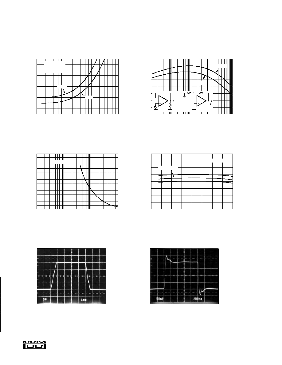
TOTAL HARMONIC DISTORTION + NOISE
vs FREQUENCY
Frequency (Hz)
THD + N (%)
1
0.1
0.01
0.001
0.0001
20
100
1k
10k
20k
G = 100V/V
G = 10V/V
G = 1V/V
Measurement BW = 80kHz
See "Distortion Measure-
ments" for description of
test method.
1k
V =
3.5Vrms
O
OPEN-LOOP GAIN/PHASE vs FREQUENCY
Frequency (Hz)
Voltage Gain (dB)
120
100
80
60
40
20
0
≠20
1
10
100
1k
10k
100k
1M
10M
0
≠45
≠90
≠135
≠180
Phase Shift (Degrees)
G
INPUT BIAS AND INPUT OFFSET CURRENT
vs TEMPERATURE
Ambient Temperature (∞C)
Input Bias Current (pA)
≠75
100nA
10nA
1nA
100
10
1
Input Offset Current (pA)
10nA
1nA
100
10
1
0.1
≠50
≠25
0
25
50
75
100
125
Input
Offset Current
Input
Bias Current
TOTAL HARMONIC DISTORTION + NOISE
vs OUTPUT VOLTAGE
Output Voltage (Vp-p)
THD + N (%)
0.1
1
10
100
0.1
0.01
0.001
0.0001
1k
V
O
f = 1kHz
Measurement BW = 80kHz
See "Distortion Measurements"
for description of test method.
INPUT VOLTAGE AND CURRENT NOISE
SPECTRAL DENSITY vs FREQUENCY
Frequency (Hz)
Voltage Noise (nV/ Hz)
1
1k
100
10
1
10
100
1k
10k
100k
1M
Current Noise (fA/ Hz)
1k
100
10
1
Voltage Noise
Current Noise
INPUT BIAS AND INPUT OFFSET CURRENT
vs INPUT COMMON-MODE VOLTAGE
Common-Mode Voltage (V)
Input Bias Current (pA)
≠15
10nA
1nA
100
10
Input Offset Current (pA)
1nA
100
10
1
≠10
≠5
0
5
10
15
Input
Offset Current
Input
Bias Current
5
OPA2604
Æ
TYPICAL PERFORMANCE CURVES
(CONT)
At T
A
= +25
∞
C, V
S
=
±
15V, unless otherwise noted.
INPUT BIAS CURRENT
vs TIME FROM POWER TURN-ON
Time After Power Turn-On (min)
Input Bias Current (pA)
0
1nA
100
10
1
1
2
3
4
5
V
S
= ±24VDC
V
S
= ±15VDC
V
S
= ±5VDC
COMMON-MODE REJECTION
vs COMMON-MODE VOLTAGE
Common-Mode Voltage (V)
Common-Mode Rejection (dB)
≠15
120
110
100
90
80
≠10
≠5
0
5
10
15
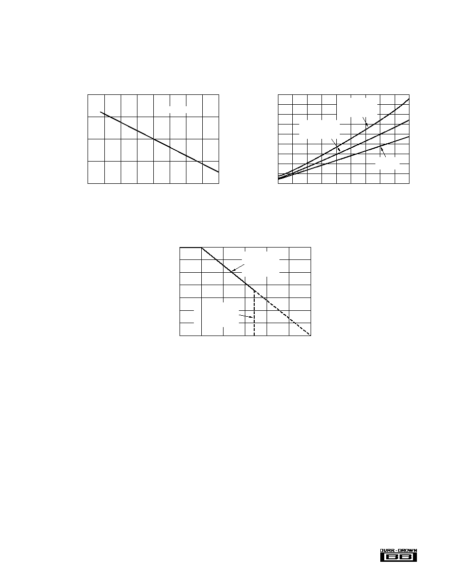
GAIN-BANDWIDTH AND SLEW RATE
vs SUPPLY VOLTAGE
Supply Voltage (±V
S
)
Gain-Bandwidth (MHz)
5
28
24
20
16
12
10
15
20
25
Slew Rate
Gain-Bandwidth
G = +100
Slew Rate (V/µs)
33
29
25
21
17
GAIN-BANDWIDTH AND SLEW RATE
vs TEMPERATURE
Temperature (∞C)
Gain-Bandwidth (MHz)
≠75
28
24
20
16
12
≠25
25
75
125
Slew Rate (V/µs)
30
25
20
15
10
≠50
0
50
100
Slew Rate
Gain-Bandwidth
G = +100
A
OL
, PSR, AND CMR vs SUPPLY VOLTAGE
Supply Voltage (±V
S
)
A
OL
, PSR, CMR (dB)
5
120
110
100
90
80
70
10
15
20
25
CMR
A
OL
PSR
POWER SUPPLY AND COMMON-MODE
REJECTION vs FREQUENCY
Frequency (Hz)
PSR, CMR (dB)
10
120
100
80
60
40
20
0
100
1k
10k
100k
1M
10M
CMR
≠PSR
+PSR
OPA2604
Æ
6
TYPICAL PERFORMANCE CURVES
(CONT)
At T
A
= +25
∞
C, V
S
=
±
15V, unless otherwise noted.
25
Slew Rate (V/µs)
30
25
20
15
10
SETTLING TIME vs CLOSED-LOOP GAIN
Closed-Loop Gain (V/V)
Settling Time (µs)
≠1
5
4
3
2
1
0
≠10
≠100
≠1000
0.01%
0.1%
V
O
= 10V Step
R
L
= 1k
C
L
= 50pF
CHANNEL SEPARATION vs FREQUENCY
Frequency (Hz)
Channel Separation (dB)
10
160
140
120
100
80
100
1k
10k
100k
V
O
=
20Vp-p
A
B
R
L
R
L
= 1k
R
L
=
Measured
Output
MAXIMUM OUTPUT VOLTAGE SWING vs FREQUENCY
Frequency (Hz)
Output Voltage (Vp-p)
10k
30
20
10
0
100k
1M
10M
V = ±15V
S
SUPPLY CURRENT vs TEMPERATURE
Ambient Temperature (∞C)
Supply Current (mA)
≠75
14
12
10
8
6
≠50
≠25
0
25
50
75
100
125
V
S
= ±24VDC
V
S
= ±15VDC
V
S
= ±5VDC
Total for Both Op Amps
≠10
FPO
Bleed to edge
0 5 10
+10
LARGE-SIGNAL TRANSIENT RESPONSE
Time (µs)
Output Voltage (V)
0
1
µ
s
2
µ
s
+100
≠100
SMALL-SIGNAL TRANSIENT RESPONSE
Time (µs)
Output Voltage (mV)
7
OPA2604
Æ
TYPICAL PERFORMANCE CURVES
(CONT)
At T
A
= +25
∞
C, V
S
=
±
15V, unless otherwise noted.
SHORT-CIRCUIT CURRENT vs TEMPERATURE
Ambient Temperature (∞C)
Short-Circuit Current (mA)
≠75
60
50
40
30
20
≠50
≠25
0
25
50
75
100
125
I
SC+
and I
SC≠
Supply Voltage, ±V
S
(V)
6
8
10
12
14
16
18
20
22
24
1
0.9
0.8
0.7
0.6
0.5
0.4
0.3
0.2
0.1
Power Dissipation (W)
POWER DISSIPATION vs SUPPLY VOLTAGE
No signal
or no load
Typical high-level
music R
L
= 600
(both channels)
Worst case sine
wave R
L
= 600
(both channels)
Ambient Temperature (∞C)
0
1.4
1.2
1.0
0.8
0.6
0.4
0.2
0
Total Power Dissipation (W)
MAXIMUM POWER DISSIPATION vs TEMPERATURE
25
50
75
100
125
150
J-A
= 90∞C/W
Soldered to
Circuit Board
(see text)
Maximum
Specified Operating
Temperature
85∞C
OPA2604
Æ
8
APPLICATIONS INFORMATION
The OPA2604 is unity-gain stable, making it easy to use in a
wide range of circuitry. Applications with noisy or high
impedance power supply lines may require decoupling ca-
pacitors close to the device pins. In most cases 1
µ
F tantalum
capacitors are adequate.
DISTORTION MEASUREMENTS
The distortion produced by the OPA2604 is below the mea-
surement limit of virtually all commercially available equip-
ment. A special test circuit, however, can be used to extend the
measurement capabilities.
Op amp distortion can be considered an internal error source
which can be referred to the input. Figure 1 shows a circuit
which causes the op amp distortion to be 101 times greater
than normally produced by the op amp. The addition of R
3
to
the otherwise standard non-inverting amplifier configuration
alters the feedback factor or noise gain of the circuit. The
closed-loop gain is unchanged, but the feedback available for
error correction is reduced by a factor of 101. This extends the
measurement limit, including the effects of the signal-source
purity, by a factor of 101. Note that the input signal and load
applied to the op amp are the same as with conventional
feedback without R
3
.
Validity of this technique can be verified by duplicating
measurements at high gain and/or high frequency where the
distortion is within the measurement capability of the test
equipment. Measurements for this data sheet were made with
the Audio Precision System One which greatly simplifies
such repetitive measurements. The measurement technique
can, however, be performed with manual distortion measure-
ment instruments.
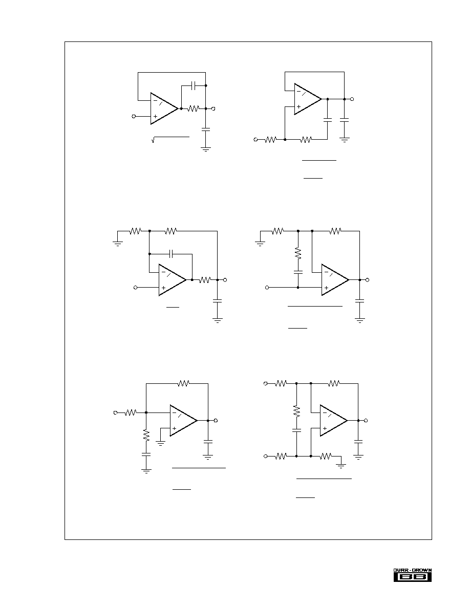
CAPACITIVE LOADS
The dynamic characteristics of the OPA2604 have been
optimized for commonly encountered gains, loads and oper-
ating conditions. The combination of low closed-loop gain
and capacitive load will decrease the phase margin and may
lead to gain peaking or oscillations. Load capacitance reacts
with the op amp's open-loop output resistance to form an
additional pole in the feedback loop. Figure 2 shows various
circuits which preserve phase margin with capacitive load.
Request Application Bulletin AB-028 for details of analysis
techniques and applications circuits.
For the unity-gain buffer, Figure 2a, stability is preserved by
adding a phase-lead network, R
C
and C
C
. Voltage drop across
R
C
will reduce output voltage swing with heavy loads. An
alternate circuit, Figure 2b, does not limit the output with low
load impedance. It provides a small amount of positive feed-
back to reduce the net feedback factor. Input impedance of this
circuit falls at high frequency as op amp gain rolloff reduces
the bootstrap action on the compensation network.
Figures 2c and 2d show compensation techniques for
noninverting amplifiers. Like the follower circuits, the circuit
in Figure 2d eliminates voltage drop due to load current, but
at the penalty of somewhat reduced input impedance at high
frequency.
Figures 2e and 2f show input lead compensation networks for
inverting and difference amplifier configurations.
NOISE PERFORMANCE
Op amp noise is described by two parameters--noise voltage
and noise current. The voltage noise determines the noise
performance with low source impedance. Low noise bipolar-
input op amps such as the OPA27 and OPA37 provide very
low voltage noise. But if source impedance is greater than a
few thousand ohms, the current noise of bipolar-input op amps
react with the source impedance and will dominate. At a few
thousand ohms source impedance and above, the OPA2604
will generally provide lower noise.
FIGURE 1. Distortion Test Circuit.
R
2
1
2
OPA2604
R
1
R
3
V
O
= 10Vp-p
(3.5Vrms)
Generator
Output
Analyzer
Input
Audio Precision
System One
Analyzer*
R
L
1k
IBM PC
or
Compatible
SIG.
GAIN
DIST.
GAIN
R
1
R
2
R
3
500
50
5k
5k
5k
50
500
1
10
100
101
101
101
* Measurement BW = 80kHz
9
OPA2604
Æ
FIGURE 2. Driving Large Capacitive Loads.
NOTE: Design equations and component values are approximate. User adjustment is required for optimum performance.
C
C
820pF
R
C
750
C
L
5000pF
e
i
C
C
=
120 X 10
≠12
C
L
(a)
e
o
C
L
5000pF
e
i
R
C
=
(b)
R
C
10
C
C
0.47µF
R
2
2k
R
2
4C
L
X 10
10
≠ 1
C
C
=
C
L
X 10
3
R
C
e
o
C
L
5000pF
R
2
10k
R
1
10k
C
C
=
50
R
2
C
L
e
i
R
C
25
C
C
24pF
(c)
e
o
C
L
5000pF
C
L
5000pF
R
2
2k
R
1
2k
e
i
R
C
20
C
C
0.22µF
(d)
R
C
=
R
2
2C
L
X 10
10
≠ (1 + R
2
/R
1
)
e
o
C
L
5000pF
R
2
2k
R
1
2k
e
i
R
C
20
C
C
0.22µF
(e)
R
C
=
R
2
2C
L
X 10
10
≠ (1 + R
2
/R
1
)
e
o
R
2
2k
R
1
2k
e
1
R
C
20
C
C
0.22µF
(f)
R
C
=
R
2
2C
L
X 10
10
≠ (1 + R
2
/R
1
)
R
3
2k
e
2
R
4
2k
e
o
1
2
OPA2604
1
2
OPA2604
1
2
OPA2604
1
2
OPA2604
1
2
OPA2604
1
2
OPA2604
C
C
=
C
L
X 10
3
R
C
C
C
=
C
L
X 10
3
R
C
C
C
=
C
L
X 10
3
R
C

OPA2604
Æ
10
Copper leadframe construction used in the OPA2604 im-
proves heat dissipation compared to conventional plastic
packages. To achieve best heat dissipation, solder the device
directly to the circuit board and use wide circuit board traces.
OUTPUT CURRENT LIMIT
Output current is limited by internal circuitry to approxi-
mately
±
40mA at 25
∞
C. The limit current decreases with
increasing temperature as shown in the typical curves.
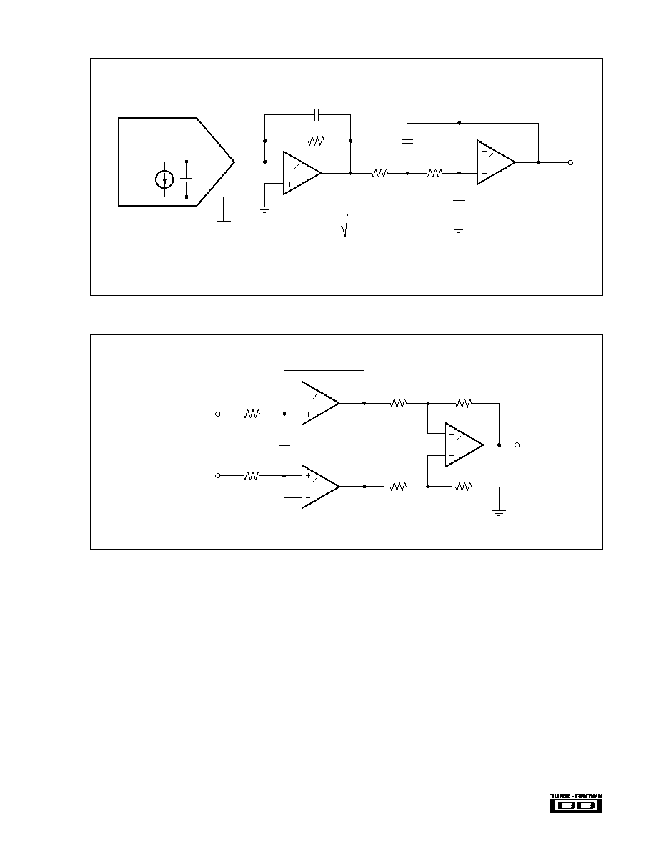
FIGURE 4. Three-Pole Generalized Immittance Converter (GIC) Low-Pass Filter.
R
5
2k
V
O
C
3
1000pF
Low-pass
3-pole Butterworth
f
≠3dB
= 40kHz
R
1
6.04k
V
IN
R
2
4.02k
R
2
4.02k
C
2
1000pF
C
1
1000pF
R
4
5.36k
See Application Bulletin AB-026
for information on GIC filters.
1
2
OPA2604
1
2
OPA2604
1
2
OPA2604
FIGURE 3. Three-Pole Low-Pass Filter.
POWER DISSIPATION
The OPA2604 is capable of driving 600
loads with power
supply voltages up to
±
24V. Internal power dissipation is
increased when operating at high power supply voltage. The
typical performance curve, Power Dissipation vs Power Sup-
ply Voltage, shows quiescent dissipation (no signal or no
load) as well as dissipation with a worst case continuous sine
wave. Continuous high-level music signals typically produce
dissipation significantly less than worst case sine waves.
R
4
22k
R
3
10k
V
O
C
2
2000pF
R
2
22k
C
1
3000pF
R
1
2.7k
V
IN
f
p
= 20kHz
C
3
100pF
1
2
OPA2604
11
OPA2604
Æ
FIGURE 6. Differential Amplifier with Low-Pass Filter.
FIGURE 5. DAC I/V Amplifier and Low-Pass Filter.
V
O
G = 1
100pF
≠
V
IN
+
7.87k
7.87k
10k
10k
10k
10k
100kHz Input Filter
1
2
OPA2604
1
2
OPA2604
1
2
OPA2604
R
3
21k
V
O
R
2
2.94k
R
1
= Feedback resistance = 2k
f
c
= Crossover frequency = 8MHz
I-Out DAC
C
3
470pF
C
1
*
C
2
2200pF
R
1
2k
* C
1
=
C
OUT
2
R
1
f
c
C
OUT
Low-pass
2-pole Butterworth
f
≠3dB
= 20kHz
~
1
2
OPA2604
1
2
OPA2604
OPA2604
Æ
12
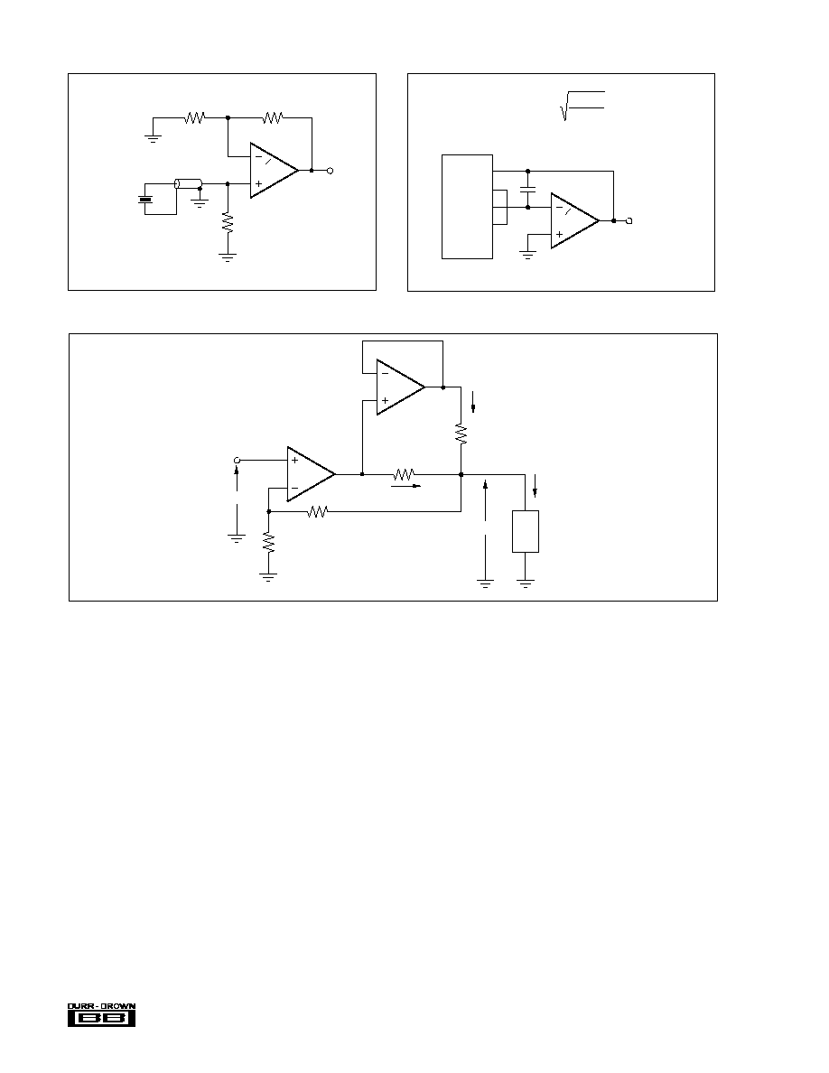
FIGURE 7. High Impedance Amplifier.
FIGURE 9. Using the Dual OPA2604 Op Amp to Double the Output Current to a Load.
FIGURE 8. Digital Audio DAC I-V Amplifier.
V
O
= ±3Vp
R
f
= Internal feedback resistance = 1.5k
f
c
= Crossover frequency = 8MHz
C
1
*
* C
1
C
OUT
2
R
f
f
c
To low-pass
filter.
1
2
OPA2604
5
6
9
PCM63
20-bit
D/A
Converter
10
A
1
A
2
V
IN
R
1
R
2
i
1
R
4
51
I
2
1/2 OPA2604
R
3
51
I
L
= I
1
+ I
2
Load
V
OUT
= V
IN
(1 + R
2
/R
1
)
V
OUT
1/2 OPA2604
G = 101
(40dB)
100
10k
Piezoelectric
Transducer
1M
*
* Provides input bias
current return path.
OPA2604
1
2

PACKAGING INFORMATION
ORDERABLE DEVICE
STATUS(1)
PACKAGE TYPE
PACKAGE DRAWING
PINS
PACKAGE QTY
OPA2604AP
ACTIVE
PDIP
P
8
50
OPA2604AU
ACTIVE
SOIC
D
8
100
OPA2604AU/2K5
ACTIVE
SOIC
D
8
2500
(1) The marketing status values are defined as follows:
ACTIVE: Product device recommended for new designs.
LIFEBUY: TI has announced that the device will be discontinued, and a lifetime-buy period is in effect.
NRND: Not recommended for new designs. Device is in production to support existing customers, but TI does not recommend using this part in
a new design.
PREVIEW: Device has been announced but is not in production. Samples may or may not be available.
OBSOLETE: TI has discontinued the production of the device.
PACKAGE OPTION ADDENDUM
www.ti.com
3-Oct-2003

IMPORTANT NOTICE
Texas Instruments Incorporated and its subsidiaries (TI) reserve the right to make corrections, modifications,
enhancements, improvements, and other changes to its products and services at any time and to discontinue
any product or service without notice. Customers should obtain the latest relevant information before placing
orders and should verify that such information is current and complete. All products are sold subject to TI's terms
and conditions of sale supplied at the time of order acknowledgment.
TI warrants performance of its hardware products to the specifications applicable at the time of sale in
accordance with TI's standard warranty. Testing and other quality control techniques are used to the extent TI
deems necessary to support this warranty. Except where mandated by government requirements, testing of all
parameters of each product is not necessarily performed.
TI assumes no liability for applications assistance or customer product design. Customers are responsible for
their products and applications using TI components. To minimize the risks associated with customer products
and applications, customers should provide adequate design and operating safeguards.
TI does not warrant or represent that any license, either express or implied, is granted under any TI patent right,
copyright, mask work right, or other TI intellectual property right relating to any combination, machine, or process
in which TI products or services are used. Information published by TI regarding third-party products or services
does not constitute a license from TI to use such products or services or a warranty or endorsement thereof.
Use of such information may require a license from a third party under the patents or other intellectual property
of the third party, or a license from TI under the patents or other intellectual property of TI.
Reproduction of information in TI data books or data sheets is permissible only if reproduction is without
alteration and is accompanied by all associated warranties, conditions, limitations, and notices. Reproduction
of this information with alteration is an unfair and deceptive business practice. TI is not responsible or liable for
such altered documentation.
Resale of TI products or services with statements different from or beyond the parameters stated by TI for that
product or service voids all express and any implied warranties for the associated TI product or service and
is an unfair and deceptive business practice. TI is not responsible or liable for any such statements.
Following are URLs where you can obtain information on other Texas Instruments products and application
solutions:
Products
Applications
Amplifiers
amplifier.ti.com
Audio
www.ti.com/audio
Data Converters
dataconverter.ti.com
Automotive
www.ti.com/automotive
DSP
dsp.ti.com
Broadband
www.ti.com/broadband
Interface
interface.ti.com
Digital Control
www.ti.com/digitalcontrol
Logic
logic.ti.com
Military
www.ti.com/military
Power Mgmt
power.ti.com
Optical Networking
www.ti.com/opticalnetwork
Microcontrollers
microcontroller.ti.com
Security
www.ti.com/security
Telephony
www.ti.com/telephony
Video & Imaging
www.ti.com/video
Wireless
www.ti.com/wireless
Mailing Address:
Texas Instruments
Post Office Box 655303 Dallas, Texas 75265
Copyright
2003, Texas Instruments Incorporated