1
Æ
OPA2607
©
2000 Burr-Brown Corporation
PDS-1615A
Printed in U.S.A. August, 2000
Dual, High Output, Current-Feedback
OPERATIONAL AMPLIFIER
DESCRIPTION
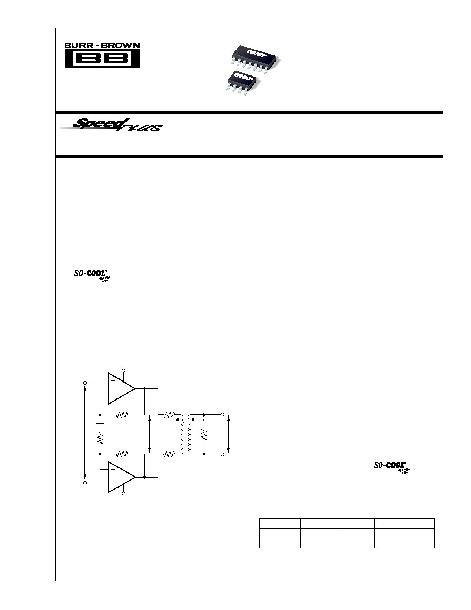
The OPA2607 provides a high output voltage swing and low
distortion required for low turns ratio ADSL upstream driver
applications. Operating on a
±
12V supply, the OPA2607 con-
sumes a low 8.0mA/channel quiescent current to deliver a very
high 250mA peak output current. Guaranteed output current of
180mA supports even the most demanding ADSL CPE require-
ments with low harmonic distortion. Differential driver applica-
tions will deliver < ≠75dBc distortion at the peak upstream power
levels of full rate ADSL. Using a differential driver design, as
shown below, the OPA2607 can deliver a high 38Vp-p voltage
swing into a 1:0.8 step-down transformer to meet the ADSL CPE
upstream power requirements. This low turns ratio actually pro-
vides a step up to the much weaker downstream signal arriving on
the line side of this transformer, extending the DSL modem's
reach.
Power control features are included in the SO-14 package version
to allow system power to be minimized. Two logic control lines
allow four quiescent power settings. These include full power,
power cutback for short loops, idle state for no signal transmission
but line match maintenance, and shutdown for power off with a
high impedance output. An additional I
ADJ
pin allows the maxi-
mum supply current to be adjusted
±
25% from the nominal value.
Connecting this pin to +V
CC
will increase the full power quiescent
to 20mA, increasing the peak output current available, while
connecting this pin to ≠V
CC
will decrease the full power quiescent
to 12mA where a lower peak output current is required. The
digital control lines continue to scale the total quiescent current
from these new maximum levels in the same proportional steps as
before.
The OPA2607 is available in three package styles. For power
driver applications, a thermally enhanced
package
with a heat slug is available in both SO-8 and SO-14 pinouts. For
lower power receiver applications, a standard SO-8 package is
available.
OPA2607
Æ
FEATURES
q
WIDEBAND
±
12V OPERATION: 25MHz (G = +8)
q
UNITY GAIN STABLE: 35MHz (G = +1)
q
HIGH OUTPUT CURRENT: 250mA
q
OUTPUT VOLTAGE SWING:
±
10.5V (V
S
=
±
12V)
q
HIGH SLEW RATE: 600V/
µ
s
q
LOW SUPPLY CURRENT: 8mA/channel
q
FLEXIBLE POWER CONTROL (SO-14)
q
±
6V TO
±
16V SUPPLY RANGE
q
POWER PACKAGING
APPLICATIONS
q
xDSL LINE DRIVER
q
LOW-NOISE ADSL RECEIVER
q
LOW-COST VIDEO DA
q
LOW-COST UPGRADE TO LT1207/AD812
TM
International Airport Industrial Park ∑ Mailing Address: PO Box 11400, Tucson, AZ 85734 ∑ Street Address: 6730 S. Tucson Blvd., Tucson, AZ 85706 ∑ Tel: (520) 746-1111
Twx: 910-952-1111 ∑ Internet: http://www.burr-brown.com/ ∑ Cable: BBRCORP ∑ Telex: 066-6491 ∑ FAX: (520) 889-1510 ∑ Immediate Product Info: (800) 548-6132
OPA2607 RELATED PRODUCTS
SINGLES
DUALS
TRIPLES
NOTES
OPA681
OPA2681
OPA3681
Single +12V Capable
--
OPA2677
--
Single +12V Capable
Low Turns Ratio ADSL Upstream Driver
348
100nF
78.7
100
4.8Vp-p
1.21k
1.21k
1/2
OPA2607
1/2
OPA2607
+12V
≠12V
1:0.8
15Vp-p
38Vp-p
78.7
For most current data sheet and other product
information, visit www.burr-brown.com
OPA2607
OPA2607
SBOS128

2
Æ
OPA2607
SPECIFICATIONS: V
S
=
±
12V
R
F
= 1.21k
, R
L
= 100
, and G = +8, unless otherwise noted.
OPA2607H, U, N
TYP
GUARANTEED
0
∞
C to
≠40
∞
C to
MIN/
TEST
PARAMETER
CONDITIONS
+25
∞
C
+25
∞
C
(2)
70
∞
C
(3)
+85
∞
C
(3)
UNITS
MAX
LEVEL
(1)
AC PERFORMANCE (see Figure 1)
Small-Signal Bandwidth (V
O
= 0.5Vp-p)
G = +1, R
F
= 1.50k
35
MHz
typ
C
G = +2, R
F
= 1.43k
28
MHz
typ
C
G = +4, R
F
= 1.37k
25
MHz
typ
C
G = +8, R
F
= 1.21k
25
19
18
17
MHz
min
B
Bandwidth for 0.1dB Gain Flatness
G = +8, V
O
= 0.5Vp-p
6
MHz
typ
C
Large-Signal Bandwidth
G = +8, V
O
= 20Vp-p
13
10.6
9.0
7.9
MHz
min
B
Slew Rate
G = +8, V
O
= 20V Step
600
470
400
350
V/
µ
s
min
B
Rise/Fall Time
G = +8, V
O
= 0.5V Step
14
18
20
21
ns
min
B
Spurious Free Dynamic Range
(4)
V
O
= 2Vp-p, 1MHz, R
L
= 100
77
66
60
57
dB
min
B
V
O
= 20Vp-p, 150kHz, R
L
= 150
75
70
58
57
dB
min
B
Input Voltage Noise
1.7
2.0
2.6
2.7
nV/
Hz
max
B
Non-Inverting Input Current Noise
11
13
13
13
pA/
Hz
max
B
Inverting Input Current Noise
15
17
17
17
pA/
Hz
max
B
Differential Gain
NTSC, G = +2, R
L
= 150
0.01
%
typ
C
Differential Phase
NTSC, G = +2, R
L
= 150
0.01
degrees
typ
C
Channel-to-Channel Crosstalk
f = 1MHz
≠60
dB
typ
C
DC PERFORMANCE
(5)
Open-Loop Transimpedance Gain
V
O
= 0V, R
L
= 100
950
440
390
310
k
min
A
Input Offset Voltage
V
CM
= 0V
±
1.5
±
7
±
8
±
8.5
mV
max
A
Average Offset Voltage Drift
V
CM
= 0V
≠20
≠25
µ
V/
∞
C
max
B
Non-Inverting Input Bias Current
V
CM
= 0V
±
3
±
12
±
15
±
20
µ
A
max
A
Average Non-Inverting Input Bias Current Drift
V
CM
= 0V
≠70
≠100
nA/
∞
C
max
B
Inverting Input Bias Current
V
CM
= 0V
±
4
±
40
±
58
±
70
µ
A
max
A
Average Inverting Input Bias Current Drift
V
CM
= 0V
≠380
≠425
nA/
∞
C
max
B
INPUT
Common-Mode Input Range (CMIR)
±
10.3
±
10.0
±
9.9
±
9.8
V
min
A
Common-Mode Rejection Ratio (CMRR)
V
CM
= 0V
64
53
52
51
dB
min
A
Non-Inverting Input Impedance
250 || 4
k
|| pF
typ
C
Inverting Input Resistance
Open-Loop
33
typ
C
OUTPUT
Voltage Output Swing
No Load, Hard Limit
±
11.2
±
10.9
±
10.8
±
10.7
V
min
A
R
L
= 100
, Hard Limit
±
10.5
±
9.9
±
9.8
±
9.7
V
min
A
R
L
= 150
, SFDR > 67dB, 150kHz
±
10.2
V
typ
C
Current Output, Sourcing
V
O
= 0
310
210
175
140
mA
min
A
Current Output, Sinking
V
O
= 0
250
180
150
110
mA
min
A
Closed-Loop Output Impedance
G = +8, f
10kHz
0.02
typ
C
Power Control (SO-14 only)
DIG_REF = Gnd
Maximum Logic 0
A0, A1
0.8
V
max
C
Minimum Logic 1
A0, A1
2
V
min
C
Logic Input Current
0V to 4.5V
60
µ
A
max
C
Supply Current at Full Power
A0 = 1, A1 = 1, I
ADJ
= open
16
mA
typ
C
Supply Current at Power Cutback
A0 = 0, A1 = 1, I
ADJ
= open
13
mA
typ
C
Supply Current at Idle Power
A0 = 1, A1 = 0, I
ADJ
= open
3.8
mA
typ
C
Supply Current at Shutdown
A0 = 0, A1 = 0, I
ADJ
= open
1.3
mA
typ
C
Output Impedance in Idle Power
Closed-Loop, f < 1MHz
0.7
typ
C
Output Impedance in Shutdown
350 || 17
k
|| pF
typ
C
Shutdown Isolation
G = +8, 1MHz
75
dB
typ
C
Maximum Adjusted Quiescent Current
A0 = 1, A1 = 1, I
ADJ
at +V
S
20
mA
typ
C
Minimum Adjusted Quiescent Current
A0 = 1, A1 = 1, I
ADJ
at ≠V
S
12
mA
typ
C
POWER SUPPLY
Minimum Operating Voltage
±
6
±
6
±
6
V
min
B
Specified Operating Voltage
±
12
V
typ
C
Maximum Operating Voltage
±
16
±
16
±
16
V
max
A
Maximum Quiescent Current
Total Both Channels, Full Power
16
16.8
17
17.5
mA
max
A
Minimum Quiescent Current
Total Both Channels, Full Power
16
15.2
13.8
13.3
mA
min
A
Power Supply Rejection Ratio (PSRR)
f
10kHz
68
61
59
57
dB
min
A
TEMPERATURE RANGE
Specification: H, U, N
≠40 to +85
∞
C
typ
C
Thermal Resistance,
JA
Junction-to-Ambient
H
PSO-8 Power Package
(6)
50
∞
C/W
typ
C
U
SO-8
125
∞
C/W
typ
C
N
PSO-14 Power Package
(6)
45
∞
C/W
typ
C
NOTES: (1) Test Levels: (A) 100% tested at 25
∞
C. Over temperature limits by characterization and simulation. (B) Limits set by characterization and simulation.
(C) Typical value only for information. (2) Junction temperature = ambient for 25
∞
C guaranteed specifications. (3) Junction temperature = ambient at low temperature
limit: junction temperature = ambient +40
∞
C at high temperature limit for over temperature guaranteed specifications. (4) Single amplifier SFDR limited by 2nd Harmonic.
Differential SFDR will be limited by 3rd Harmonic and will be > 15dB higher. (5) Current is considered positive out of node. V
CM
is the input common-mode voltage.
(6) Slug in power package connected to ≠V
S
plane at least 2" x 2" (50mm x 50mm) in size. See the Board Layout Guidelines Section.
3
Æ
OPA2607
ABSOLUTE MAXIMUM RATINGS
Power Supply .............................................................................
±
16.5V
DC
Internal Power Dissipation
(1)
............................ See Thermal Information
Differential Input Voltage .....................................................................
±
5V
Input Voltage Range ............................................................................
±
V
S
Storage Temperature Range: U, N ................................ ≠40
∞
C to +125
∞
C
Lead Temperature (soldering, 10s) .............................................. +260
∞
C
Junction Temperature (T
J
) ........................................................... +175
∞
C
ESD Rating (Human Body Model) .................................................. 4000V
(Machine Model) ........................................................... 300V
NOTE:: (1) Packages must be derated based on specified
JA
. Maximum T
J
must be observed.
ELECTROSTATIC
DISCHARGE SENSITIVITY
Electrostatic discharge can cause damage ranging from perfor-
mance degradation to complete device failure. Burr-Brown
Corporation recommends that all integrated circuits be handled
and stored using appropriate ESD protection methods.
ESD damage can range from subtle performance degradation to
complete device failure. Precision integrated circuits may be
more susceptible to damage because very small parametric
changes could cause the device not to meet published specifica-
tions.
The information provided herein is believed to be reliable; however, BURR-BROWN assumes no responsibility for inaccuracies or omissions. BURR-BROWN assumes
no responsibility for the use of this information, and all use of such information shall be entirely at the user's own risk. Prices and specifications are subject to change
without notice. No patent rights or licenses to any of the circuits described herein are implied or granted to any third party. BURR-BROWN does not authorize or warrant
any BURR-BROWN product for use in life support devices and/or systems.
PIN CONFIGURATIONS
Top View
PACKAGE
SPECIFIED
DRAWING
TEMPERATURE
PACKAGE
ORDERING
TRANSPORT
PRODUCT
PACKAGE
NUMBER
RANGE
MARKING
NUMBER
(1)
MEDIA
OPA2607H
PSO-8
182-1
≠40
∞
C to +85
∞
C
OPA2607H
OPA2607H
Rails
"
"
"
"
"
OPA2607H/2K5
Tape and Reel
OPA2607U
SO-8
182
"
OPA2607U
OPA2607U
Rails
"
"
"
"
"
OPA2607U/2K5
Tape and Reel
OPA2607N
PSO-14
235-1
"
OPA2607N
Contact Factory
Rails
"
"
"
"
"
Contact Factory
Tape and Reel
NOTE: (1) Models with a slash (/) are available only as Tape and Reel in the quantity indicated after the slash (e.g. /2K5 indicates 2500 devices per reel). Ordering 2500
pieces of the OPA2607U/2K5 will get a single 2500-piece Tape and Reel.
PACKAGE/ORDERING INFORMATION
1
2
3
4
8
7
6
5
+V
S
Out B
≠In B
+In B
SO-8, PSO-8
Out A
≠In A
+In A
≠V
S
1
2
3
4
5
6
7
14
13
12
11
10
9
8
≠In A
+In A
A0
≠V
S
A1
+In B
≠In B
Out A
NC
DIG_REF
+V
S
IADJ
NC
Out B
NC = No Connection
PSO-14
Power
Control
4
Æ
OPA2607
TYPICAL PERFORMANCE CURVES: V
S
=
±
12V
At T
A
= +25
∞
C, G = +8, R
F
= 1.21k
, and R
L
= 100
, unless otherwise noted. See Figure 1 for AC performance only.
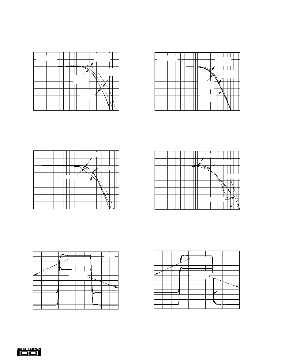
NON-INVERTING SMALL-SIGNAL
FREQUENCY RESPONSE
Frequency (Hz)
1M
10M
100M
6
3
0
≠3
≠6
≠9
≠12
≠15
≠18
Normalized Gain (dB)
V
O
= 0.5Vp-p
G = +1
R
F
= 1.50k
G = +4
R
F
= 1.37k
G = +8
R
F
= 1.21k
G = +2
R
F
= 1.43k
NON-INVERTING PULSE RESPONSE
Time (100ns/div)
Output Voltage (2V/div)
Output Voltage (100mV/div)
G = +8
V
O
= 20Vp-p
Large Signal
V
O
= 0.5Vp-p
Small Signal
INVERTING SMALL-SIGNAL
FREQUENCY RESPONSE
Frequency (Hz)
1M
10M
100M
6
3
0
≠3
≠6
≠9
≠12
≠15
≠18
Normalized Gain (dB)
G = ≠8
R
F
= 1.18k
G = ≠2
R
F
= 1.40k
G = ≠4
R
F
= 1.30k
G = ≠1
R
F
= 1.43k
V
O
= 0.5Vp-p
INVERTING PULSE RESPONSE
Time (100ns/div)
Output Voltage (2V/div)
Output Voltage (100mV/div)
G = ≠8
V
O
= 20Vp-p
Large Signal
V
O
= 0.5Vp-p
Small Signal
NON-INVERTING LARGE-SIGNAL
FREQUENCY RESPONSE
Frequency (Hz)
1M
10M
100M
6
3
0
≠3
≠6
≠9
≠12
≠15
≠18
Normalized Gain (dB)
G = +8
V
O
= 0.5Vp-p
V
O
= 2Vp-p
V
O
= 8Vp-p
V
O
= 16Vp-p
INVERTING LARGE-SIGNAL
FREQUENCY RESPONSE
Frequency (Hz)
1M
10M
100M
6
3
0
≠3
≠6
≠9
≠12
≠15
≠18
Normalized Gain (dB)
V
O
= 0.5Vp-p
V
O
= 2Vp-p
V
O
= 8Vp-p
V
O
= 16Vp-p
G = ≠8
5
Æ
OPA2607
TYPICAL PERFORMANCE CURVES: V
S
=
±
12V
(Cont.)
At T
A
= +25
∞
C, G = +8, R
F
= 1.21k
, and R
L
= 100
, unless otherwise noted. See Figure 1 for AC performance only.
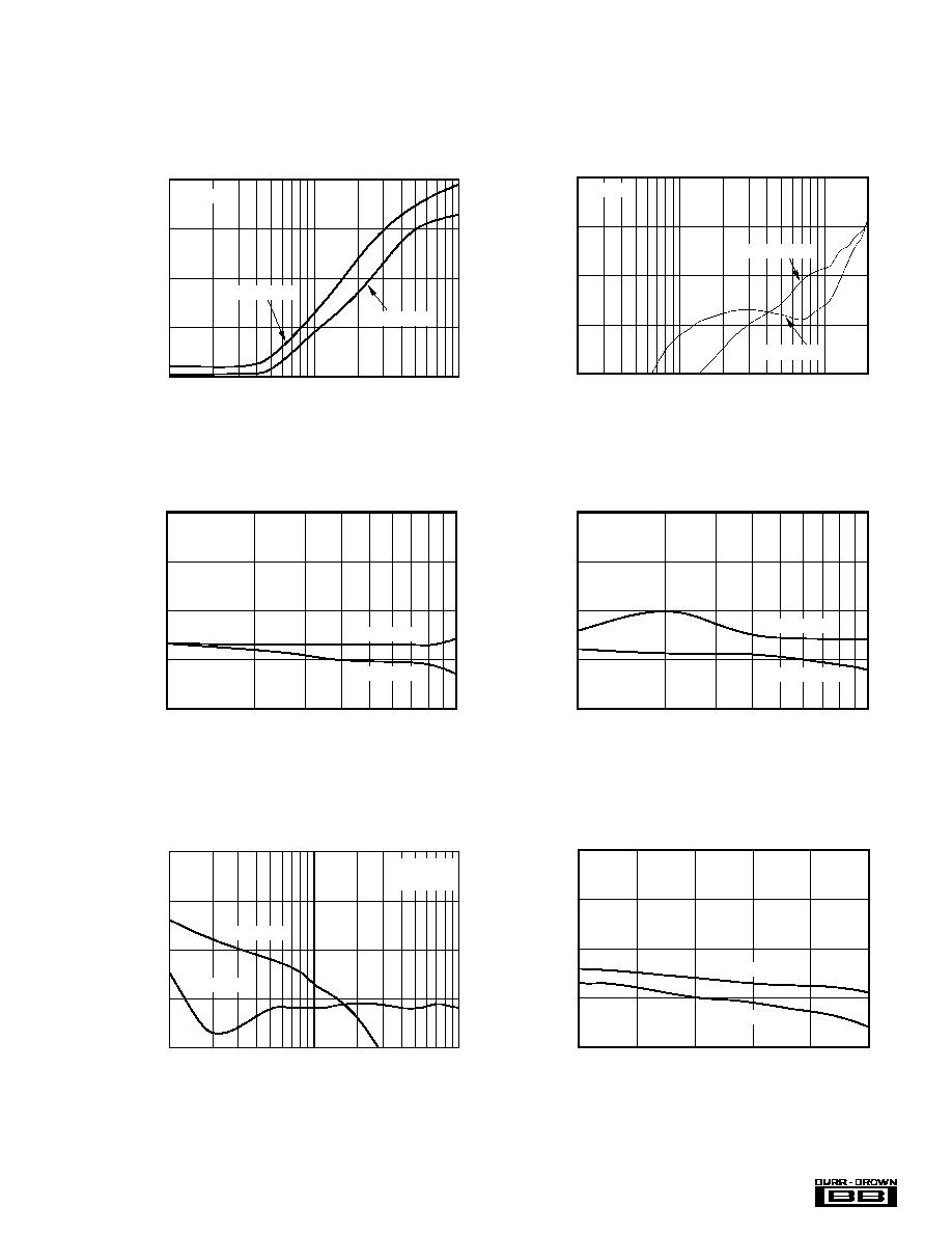
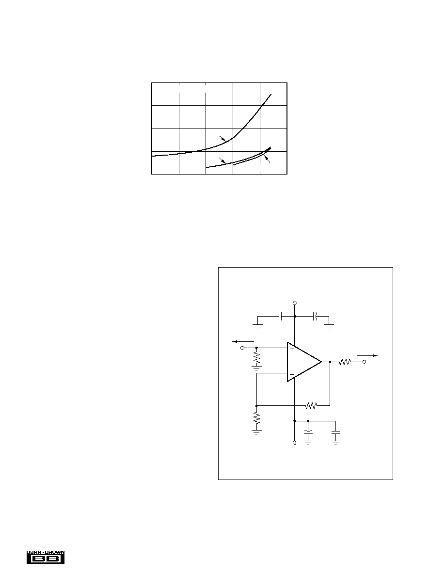
HARMONIC DISTORTION vs NON-INVERTING GAIN
Gain Magnitude (V/V)
0.1
10
≠50
≠60
≠70
≠80
≠90
Harmonic Distortion (dBc)
V
O
= 2Vp-p
f = 1MHz
3rd-Harmonic
2nd-Harmonic
HARMONIC DISTORTION vs DUAL SUPPLY VOLTAGE
Dual Supply Voltage (
±
V)
6
8
10
12
14
16
≠50
≠60
≠70
≠80
≠90
Harmonic Distortion (dBc)
V
O
= 2Vp-p
f
O
= 1MHz
3rd-Harmonic
2nd-Harmonic
HARMONIC DISTORTION vs OUTPUT VOLTAGE
Output Voltage (Vp-p)
0.1
1
20
10
≠50
≠60
≠70
≠80
≠90
Harmonic Distortion (dBc)
f = 1MHz
2nd-Harmonic
3rd-Harmonic
HARMONIC DISTORTION vs INVERTING GAIN
Gain Magnitude (≠V/V)
0.1
10
≠50
≠60
≠70
≠80
≠90
Harmonic Distortion (dBc)
V
O
= 2Vp-p
f = 1MHz
3rd-Harmonic
2nd-Harmonic
HARMONIC DISTORTION vs FREQUENCY
Frequency (Hz)
100k
1M
10M
≠50
≠60
≠70
≠80
≠90
Harmonic Distortion (dBc)
2nd-Harmonic
3rd-Harmonic
V
O
= 2Vp-p
HARMONIC DISTORTION vs LOAD RESISTANCE
Load Resistance (
)
10
100
1000
≠50
≠60
≠70
≠80
≠90
Harmonic Distortion (dBC)
2nd-Harmonic
3rd-Harmonic
V
O
= 2Vp-p
f
O
= 1MHz
6
Æ
OPA2607
APPLICATIONS INFORMATION
WIDEBAND CURRENT FEEDBACK OPERATION
The OPA2607 gives the exceptional AC performance of a
wideband current feedback op amp with a highly linear,
high power output stage. Requiring only 8.0mA/chan quies-
cent current, the OPA2607 will swing to within 2V of either
supply rail and deliver in excess of 180mA guaranteed at
room temperature. This low output headroom requirement,
along with supply-voltage independent biasing, gives re-
markable single (+15V) supply operation. Previous boosted
output stage amplifiers have typically suffered from very
poor crossover distortion as the output current goes through
zero. The OPA2607 achieves a comparable power gain with
much better linearity. The primary advantage of a current-
feedback op amp over a voltage-feedback op amp is that AC
performance (bandwidth and distortion) is relatively inde-
pendent of signal gain.
Figure 1 shows the DC-coupled, gain of +8, dual power-
supply circuit configuration used as the basis of the
±
12V
Specifications and Typical Performance Curves. For test
purposes, the input impedance is set to 50
with a resistor
to ground and the output impedance is set to 50
with a
series output resistor. Voltage swings reported in the speci-
fications are taken directly at the input and output pins while
load powers (dBm) are defined at a matched 50
load.
For the circuit of Figure 1, the total effective load will be
100
|| 1379
= 93
.
TYPICAL PERFORMANCE CURVES: V
S
=
±
12V
(Cont.)
At T
A
= +25
∞
C, G = +8, R
F
= 1.21k
, and R
L
= 100
, unless otherwise noted. See Figure 1 for AC performance only.
1/2
OPA2607
+12V
+
≠12V
50
Load
49.9
49.9
V
O
V
I
50
Source
R
G
169
R
F
1.21k
+
2.2
µ
F
0.1
µ
F
2.2
µ
F
0.1
µ
F
+V
S
≠V
S
FIGURE 1. DC-Coupled, G = +8, Bipolar Supply, Specifi-
cation and Test Circuit.
TWO-TONE,3RD-ORDER
INTERMODULATION SPURIOUS
Single-Tone Load Power (dBm)
≠5
0
5
10
15
20
≠50
≠60
≠70
≠80
≠90
3rd-Order Spurious Level (dBc)
f
O
= 2MHz
f
O
= 1MHz
Load Power at Matched 50
Load
f
O
500kHz
7
Æ
OPA2607
DESIGN-IN TOOLS
DEMONSTRATION BOARDS
Several PC boards are available to assist in the initial
evaluation of circuit performance using the OPA2607 in its
3 package styles. All are available free as an unpopulated
PC board delivered with descriptive documentation. The
summary information for these boards is shown in Table I.
The buffer gain is typically very close to 1.00 and is
normally neglected from signal gain considerations. It will,
however set the CMRR for a single op amp differential-
amplifier configuration. For a buffer gain
< 1.0, the
CMRR = ≠20
∑
log (1≠
) dB.
R
I
, the buffer output impedance, is a critical portion of the
bandwidth control equation. The OPA2607 has an R
I
typi-
cally about 33
.
A current-feedback op amp senses an error current in the
inverting node (as opposed to a differential input error
voltage for a voltage-feedback op amp) and passes this on to
the output through an internal frequency dependent
transimpedance gain. The typical performance curves show
this open-loop transimpedance response. This is analogous
to the open-loop voltage gain curve for a voltage-feedback
op amp. Developing the transfer function for the circuit of
Figure 2 gives Equation 1:
This is written in a loop-gain analysis format where the
errors arising from a finite open-loop gain are shown in the
denominator. If Z(s) were infinite over all frequencies, the
denominator of Equation 1 would reduce to 1 and the ideal
desired signal gain shown in the numerator would be achieved.
The fraction in the denominator of Equation 1 determines
the frequency response. Equation 2 shows this as the loop-
gain equation:
Contact the Burr-Brown applications support line to request
any of these boards.
MACROMODELS AND APPLICATIONS SUPPORT
Computer simulation of circuit performance using SPICE is
often useful when analyzing the performance of analog
circuits and systems. This is particularly true for video and
RF amplifier circuits where parasitic capacitance and induc-
tance can have a major effect on circuit performance. SPICE
models for some op amps are available through the Burr-
Brown web site (http://www.burr-brown.com). These mod-
els do a good job of predicting small-signal AC and transient
performance under a wide variety of operating conditions.
They do not do as well in predicting the harmonic distortion,
dG/dP, or temperature characteristics. These models do not
attempt to distinguish between the package types in their
small-signal AC performance, nor do they attempt to simu-
late channel-to-channel coupling.
OPERATING SUGGESTIONS
SETTING RESISTOR VALUES TO
OPTIMIZE BANDWIDTH
A current-feedback op amp like the OPA2607 can hold an
almost constant bandwidth over signal gain settings with the
proper adjustment of the external resistor values. This is
shown in the Typical Performance Curves; the small-signal
bandwidth decreases only slightly with increasing gain. Those
curves also show that the feedback resistor has been changed
for each gain setting. The resistor "values" on the inverting
side of the circuit for a current-feedback op amp can be
treated as frequency- response compensation elements while
their "ratios" set the signal gain. Figure 2 shows the small-
signal frequency-response analysis circuit for the OPA2607.
The key elements of this current feedback op amp model are:
Buffer Gain from the Non-inverting Input to the Inverting Input
R
I
Buffer Output Impedance
i
ERR
Feedback Error Current Signal
Z(s)
Frequency Dependent Open Loop Transimpedance Gain
from i
ERR
to V
O
DEMO BOARD
ORDERING
PRODUCT
PACKAGE
NUMBER
NUMBER
OPA2607U
SO-8
DEM-OPA268xU
MKT-352
OPA2607N
SO-14 SO-Cool
DEM-OPA2607N
MKT-367
OPA2607H
SO-8 SO-Cool
DEM-OPA2607H
MKT-366
R
F
V
O
R
G
R
I
Z
(S)
I
ERR
I
ERR
V
I
FIGURE 2. Current-Feedback Transfer Function Analysis
Circuit.
V
O
V
I
=
1
+
R
F
R
G
1
+
R
F
+
R
I
1
+
R
F
R
G
Z
(S)
=
NG
1
+
R
F
+
R
I
NG
Z
(S)
NG
1
+
R
F
R
G
(1)
Z
(S)
R
F
+
R
I
NG
=
Loop Gain
(2)
TABLE I.
8
Æ
OPA2607
If 20
∑
log (R
F
+ NG
∑
R
I
) were drawn on top of the open-
loop transimpedance plot, the difference between the two
would be the loop gain at a given frequency. Eventually,
Z(s) rolls off to equal the denominator of Equation 2 at
which point the loop gain has reduced to 1 (and the curves
have intersected). This point of equality is where the
amplifier's closed-loop frequency response given by Equa-
tion 1 will start to roll off, and is exactly analogous to the
frequency at which the noise gain equals the open-loop
voltage gain for a voltage-feedback op amp. The difference
here is that the total impedance in the denominator of
Equation 2 may be controlled somewhat separately from the
desired signal gain (or NG).
The OPA2607 is internally compensated to give a maxi-
mally flat frequency response for R
F
= 1.21k
at NG = 8 on
±
12V supplies. Evaluating the denominator of Equation 2
(which is the feedback transimpedance) gives an optimal
target of 1.44k
. As the signal gain changes, the contribu-
tion of the NG
x
R
I
term in the feedback transimpedance will
change, but the total can be held constant by adjusting R
F
.
Equation 3 gives an approximate equation for optimum R
F
over signal gain:
As the desired signal gain increases, this equation will
eventually predict a negative R
F
. A somewhat subjective
limit to this adjustment can also be set by holding R
G
to a
minimum value of 20
. Lower values will load both the
buffer stage at the input and the output stage if R
F
gets too
low--actually decreasing the bandwidth. Figure 3 shows the
recommended R
F
versus NG. The values for R
F
versus Gain
shown here are approximately equal to the values used to
generate the typical performance curves. They differ in that
the optimized values used in the typical performance curves
are also correcting for board parasitics not considered in the
simplified analysis leading to Equation 3. The values shown
in Figure 3 give a good starting point for design where
bandwidth optimization is desired.
The total impedance going into the inverting input may be
used to adjust the closed-loop signal bandwidth. Inserting a
series resistor between the inverting input and the summing
junction will increase the feedback impedance (denominator
of Equation 2), decreasing the bandwidth. The internal
buffer output impedance for the OPA2607 is slightly influ-
enced by the source impedance looking out of the non-
inverting input terminal. High-source resistors will have the
effect of increasing R
I
, decreasing the bandwidth. For those
single-supply applications which develop a midpoint bias at
the non-inverting input through high-valued resistors, the
decoupling capacitor is essential for power-supply ripple
rejection, non-inverting input-noise current shunting, and to
minimize the high frequency value for R
I
in Figure 2.
INVERTING AMPLIFIER OPERATION
Since the OPA2607 is a wideband, current-feedback op
amp, most of the familiar op amp application circuits are
available to the designer. Those dual op amp applications
that require considerable flexibility in the feedback element
(e.g. integrators, transimpedance, some filters) should con-
sider the unity gain stable voltage-feedback OPA2680, since
the feedback resistor is the compensation element for a
current-feedback op amp. Wideband inverting operations
(and especially summing) are particularly suited to the
OPA2607. Figure 4 shows a typical inverting configuration
where the I/O impedances are 50
.
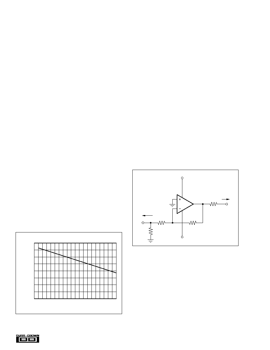
(3)
1600
1400
1200
1000
800
600
400
200
0
Noise Gain, NG (V/V)
0
20
10
15
5
FEEDBACK RESISTOR vs NOISE GAIN
Feedback Resistor, R
F
(
)
FIGURE 3. Recommended Feedback Resistor vs Noise
Gain.
1/2
OPA2607
R
F
1.21k
R
G
150
+12V
≠12V
49.9
50
Load
V
O
Power supply
de-coupling
not shown
V
I
50
Source
R
M
75.0
FIGURE 4. Inverting Gain of ≠8 with Impedance Matching.
In the inverting configuration, two key design consider-
ations must be noted. The first is that the gain resistor (R
G
)
becomes part of the signal-channel input impedance. If input
impedance matching is desired (which is beneficial when-
ever the signal is coupled through a cable, twisted pair, long
PC board trace, or other transmission line conductor), it is
normally necessary to add an additional matching resistor
(R
M
) to ground. R
G
by itself is normally not set to the
required input impedance since its value, along with the
desired gain, will determine an R
F
which may be non-
optimal from a frequency response standpoint. The total
input impedance for the source becomes the parallel combi-
nation of R
G
and R
M
.
R
NG R
F
I
=
1441
≠
9
Æ
OPA2607
NOISE PERFORMANCE
Wideband current-feedback op amps generally have a higher
output noise than comparable voltage-feedback op amps. The
OPA2607 offers an excellent balance between voltage and
current noise terms to achieve low output noise. The inverting
current noise (15pA/
Hz) is significantly lower than competi-
tive solutions, while the input voltage noise (1.7nV/
Hz) is
lower than most unity gain stable, wideband, voltage-feedback
op amps. This low input voltage noise was achieved at the
price of higher non-inverting input current noise (11pA/
Hz).
As long as the AC source impedance looking out of the non-
inverting node is less than 100
, this current noise will not
contribute significantly to the total output noise. The op amp
input voltage noise and the two input current noise terms
combine to give low output noise under a wide variety of
operating conditions. Figure 5 shows the op amp noise analy-
sis model with all the noise terms included. In this model, all
noise terms are taken to be noise voltage or current density
terms in either nV/
Hz or pA/
Hz.
The second major consideration, touched on in the previous
paragraph, is that the signal-source impedance becomes part
of the noise-gain equation and will have slight effect on the
bandwidth through Equation 1. The values shown in Figure
4 have accounted for this by slightly decreasing R
F
to re-
optimize the bandwidth for the noise gain. In the example of
Figure 4, the R
M
value combines in parallel with the external
50
source impedance, yielding an effective driving imped-
ance of 50
|| 75
= 30.0
. This impedance is added in
series with R
G
for calculating the noise gain, which gives
NG = 7.72 (instead of NG = 9.00 with a 0
source). This
value, along with the R
F
of Figure 3 and the inverting input
impedance of 33
, are inserted into Equation 3 to get
R
F
= 1186
.
Note that the non-inverting input in this bipolar-supply
inverting application is connected directly to ground. It is
often suggested that an additional resistor be connected to
ground on the non-inverting input to achieve bias-current
error cancellation at the output. The input bias currents for
a current-feedback op amp are not generally matched in
either magnitude or polarity. Connecting a resistor to ground
on the non-inverting input of the OPA2607 in the circuit of
Figure 4 will actually provide additional gain for that input's
bias and noise currents, but will not decrease the output DC
error since the input bias currents are not matched.
OUTPUT CURRENT AND VOLTAGE
The OPA2607 provides outstanding output voltage and
current capabilities. Under no-load conditions at 25
∞
C, the
output voltage typically swings within 0.8V of either supply
rail; the guaranteed swing limit is within 1.1V of either rail.
Into a 5
load (the minimum tested load), it is guaranteed to
deliver more than
±
180mA.
DISTORTION PERFORMANCE
The OPA2607 provides good distortion performance into a
100
load on
±
12V supplies. Relative to alternative solutions,
it provides exceptional performance into lighter loads.
Increasing the load impedance improves distortion directly.
Remember that the total load includes the feedback network--
in the non-inverting configuration (Figure 1) this is the sum of
R
F
+ R
G
, while in the inverting configuration it is just R
F
.
Also, providing an additional supply decoupling capacitor
(0.1
µ
F) between the supply pins (for bipolar operation) im-
proves the 2nd-order distortion slightly (3 to 6dB).
In most op amps, increasing the output voltage swing in-
creases harmonic distortion directly. As the typical perfor-
mance curves show, the spurious intermodulation powers do
not increase as predicted by a traditional intercept model.
As the fundamental power level increases, the dynamic
range does not decrease significantly. For 2 tones centered
at 1MHz, with 10dBm/tone into a matched 50
load
(i.e. 2Vp-p for each tone at the load, which requires 8Vp-p
for the overall 2-tone envelope at the output pin), the typical
performance curves show 85dBc difference between the
test-tone power and the 3rd-order intermodulation spurious
levels.
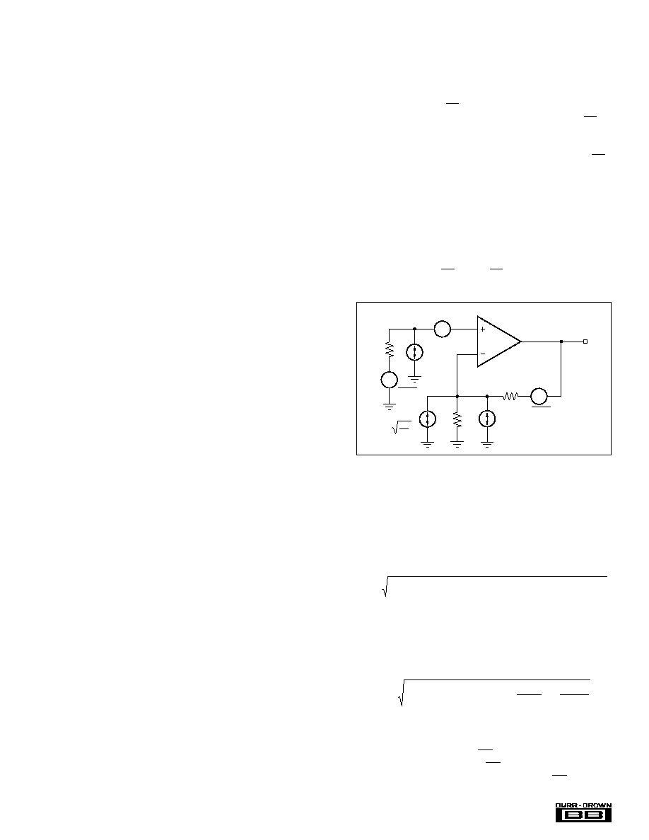
FIGURE 5. Op Amp Noise Analysis Model.
4kT
R
G
R
G
R
F
R
S
1/2
OPA2607
I
BI
E
O
I
BN
4kT = 1.6 x 10
≠20
J
at 290
∞
K
E
RS
E
NI
4kTR
S
˜
4kTR
F
˜
The total output spot noise voltage can be computed as the
square root of the sum of all squared output noise voltage
contributors. Equation 4 shows the general form for the
output noise voltage using the terms shown in Figure 5.
Dividing this expression by the noise gain (NG = (1+R
F
/R
G
))
will give the equivalent input referred spot noise voltage at the
non-inverting input as shown in Equation 5.
Evaluating these two equations for the OPA2607 circuit and
component values shown in Figure 1 will give a total output
spot noise voltage of 27nV/
Hz and a total equivalent input
spot noise voltage of 3.4nV/
Hz. This total input referred
spot noise voltage is higher than the 1.7nV/
Hz specifica-
E
E
I
R
kTR NG
I R
kTR NG
O
NI
BN
S
S
BI
F
F
=
+
(
)
+
(
)
+
(
)
+
2
2
2
2
4
4
E
E
I
R
kTR
I R
NG
kTR
NG
N
NI
BN
S
S
BI
F
F
=
+
(
)
+
+
+
2
2
2
4
4
(4)
(5)

10
Æ
OPA2607
The ADSL Upstream Driver shown on the front page will be
used as an example of these calculations. The ADSL
(G.DMT) standard uses a spectrally-efficient coding tech-
nique, which produces a near-Gaussian output voltage distri-
bution. Under these conditions, I
O(AVE)
= 0.8 I
O(RMS)
.
The maximum allowed crest factor in this standard is
CF = 5.33Vpk/Vrms. We now calculate for each amplifier
individually:
Now calculate the typical junction temperature of both
channels of the OPA2607H (PSO-8 Package)
based on Equations 6 and 7:
The junction temperature of this example is well below
175
∞
C absolute maximum because the PSO-8 power pack-
age has such a low thermal impedance when properly
connected to the ≠V
S
power plane (see the Board Layout
Guidelines section). To help illustrate this point, the regular
SO-8 package (OPA2607U) gives T
J
= 171
∞
C under the
same conditions.
BOARD LAYOUT GUIDELINES
Achieving optimum performance with a high-frequency
amplifier like the OPA2607 requires careful attention to
board layout parasitics and external component types. Rec-
ommendations that will optimize performance include:
a) Minimize parasitic capacitance to any AC ground for
all of the signal I/O pins. Parasitic capacitance on the output
and inverting input pins can cause instability. On the non-
inverting input it can react with the source impedance to
cause unintentional bandlimiting. To reduce unwanted ca-
pacitance, a window around the signal I/O pins should be
opened in all of the ground and power planes around those
pins. Otherwise, ground and power planes should be unbro-
ken elsewhere on the board.
b) Minimize the distance (< 0.25") from the power supply
pins to high frequency 0.1
µ
F decoupling capacitors. At the
device pins, the ground and power plane layout should not
be in close proximity to the signal I/O pins. Avoid narrow
power and ground traces to minimize inductance between
the pins and the decoupling capacitors. The power supply
R
L
=
+
78 7
100
2
0 8
2
.
/
.
1 21
348
2
.
k
+
=
141
I
V
R
Vp p
mA
I
I
CF
mA
mA
I
I
mA
O PK
O PK
L
O RMS
O PK
O AVE
O RMS
(
)
(
)
(
)
(
)
(
)
(
)
/
.
.
.
.
=
=
-
=
=
=
=
=
=
38
2
141
135
135
5 33
25 3
0 8
20 2
tion for the op amp voltage noise alone. This reflects the
noise added to the output by the inverting current noise times
the feedback resistor. If the feedback resistor is reduced in
high-gain configurations (as suggested previously), the total
input referred voltage noise given by Equation 5 will ap-
proach just the 1.7nV/
Hz of the op amp itself. For example,
going to a gain of +20 using R
F
= 750
will give a total
input referred noise of 2.0nV/
Hz .
DC ACCURACY AND OFFSET CONTROL
A current-feedback op amp like the OPA2607 provides
exceptional bandwidth in high gains, giving fast pulse set-
tling but only moderate DC accuracy. The typical specifica-
tions show an input offset voltage comparable to high-speed
voltage-feedback amplifiers. However, the two input bias
currents are somewhat higher and are unmatched. Whereas
bias current cancellation techniques are very effective with
most voltage-feedback op amps, they do not generally re-
duce the output DC offset for wideband current-feedback op
amps. Since the two input bias currents are unrelated in both
magnitude and polarity, matching the source impedance
looking out of each input to reduce their error contribution
to the output is ineffective. Evaluating the configuration of
Figure 1, using worst case +25
∞
C input offset voltage and
the two input bias currents, gives a worst case output offset
range equal to:
±
(NG
∑
V
OS(MAX)
)
±
(I
BN
∑
R
S
/2 ∑ NG)
±
(I
BI
∑
R
F
)
where NG = non-inverting signal gain
=
±
(8
∑
7mV)
±
(12
µ
A
∑
25
∑
8)
±
(40
µ
A
∑
1.21k
)
=
±
56.0mV
±
2.4mV
±
48.4mV
=
±
107mV
THERMAL ANALYSIS
Maximum desired junction temperature will set the maxi-
mum allowed internal power dissipating. In no case should
the maximum junction temperature exceed 175
∞
C. The op-
erating junction temperature is given by:
where T
A
is the ambient temperature, P
D
is the average
power dissipation as calculated below, and
JA
is the pack-
age thermal resistance shown in the specifications.
The total internal power dissipation of a single amplifier,
assuming bipolar supplies (
±
V
S
), is:
where I
Q
is the quiescent supply current, I
O(AVE)
is the
average output current, I
O(RMS)
is the root-mean-square out-
put current, and R
L
is the load seen by the output. Under
absolute worst case conditions, with V
O
= V
S
/2, Equation 7
becomes:
T
T
P
J
A
D
JA
=
+
P
V I
V I
I
R
D
S Q
S O AVE
O RMS
L
=
+
2
2
(
)
(
)
≠
(6)
(7)
(8)
P
V I
V
R
D
S Q
S
L
=
+
(
)
2
4
2
/
(9)
(10)
P
V
mA
V
mA
mA
W
T
C
W
C W
C
D
J
= ∑
∑
+
∑
∑
(
)
∑
=
= ∞ +
∞
=
∞
2 12
16
2
12
20 2
25 3
141
0 69
85
0 69
50
120
2
(
.
) ≠
.
.
.
∑
/

11
Æ
OPA2607
connections (on pins 4 and 7) should always be decoupled
with these capacitors. An optional supply decoupling ca-
pacitor across the two power supplies (for bipolar operation)
will improve 2nd harmonic distortion performance. Larger
(2.2
µ
F to 6.8
µ
F) decoupling capacitors, effective at lower
frequency, should also be used on the main supply pins.
These may be placed somewhat farther from the device and
may be shared among several devices in the same area of the
PC board.
c) Careful selection and placement of external compo-
nents will preserve the high-frequency performance of
the OPA2607. Resistors should be a very low reactance
type. Surface-mount resistors work best and allow a tighter
overall layout. Metal film and carbon composition axially
leaded resistors can also provide good high-frequency per-
formance. Again, keep their leads and PC board trace length
as short as possible. Never use wirewound-type resistors in
a high-frequency application. Since the output pin and in-
verting input pin are the most sensitive to parasitic capaci-
tance, always position the feedback and series output resis-
tor, if any, as close as possible to the output pin. Other
network components, such as non-inverting input termina-
tion resistors, should also be placed close to the package.
Where double-side component mounting is allowed, place
the feedback resistor directly under the package on the other
side of the board between the output and inverting input
pins. The frequency response is primarily determined by the
feedback resistor value as described previously. Increasing
its value will reduce the bandwidth, while decreasing it will
give a more peaked frequency response. The 1.21k
feed-
back resistor used in the typical performance specifications
at a gain of +8 on
±
12V supplies is a good starting point for
design. Note that a 1.50k
feedback resistor, rather than a
direct short, is recommended for the unity-gain follower
application. A current-feedback op amp requires a feedback
resistor even in the unity-gain follower configuration to
control stability.
d) Connections to other wideband devices on the board
may be made with short direct traces or through on-board
transmission lines. For short connections, consider the trace
and the input to the next device as a lumped capacitive load.
Relatively wide traces (50 to 100mils) should be used,
preferably with ground and power planes opened up around
them. Estimate the total capacitive load and set R
S
from the
plot of recommended "R
S
vs Capacitive Load". Low para-
sitic capacitive loads (< 5pF) may not need an R
S
since the
OPA2607 is nominally compensated to operate with a 2pF
parasitic load. If a long trace is required, and the 6dB signal
loss intrinsic to a doubly-terminated transmission line is
acceptable, implement a matched-impedance transmission
line using microstrip or stripline techniques (consult an ECL
design handbook for microstrip and stripline layout tech-
niques). A 50
environment is normally not necessary on
board, and in fact a higher-impedance environment will
improve distortion as shown in the "Distortion vs Load"
plots. With a characteristic board-trace impedance defined
based on board material and trace dimensions, a matching
series resistor into the trace from the output of the OPA2607
is used as well as a terminating shunt resistor at the input of
the destination device. Remember also that the terminating
impedance will be the parallel combination of the shunt
resistor and the input impedance of the destination device:
this total effective impedance should be set to match the
trace impedance. The high output voltage and current capa-
bility of the OPA2607 allows multiple destination devices to
be handled as separate transmission lines, each with their
own series and shunt terminations. If the 6dB attenuation of
a doubly-terminated transmission line is unacceptable, a
long trace can be series-terminated at the source end only.
Treat the trace as a capacitive load in this case and set the
series resistor value as shown in the plot of "R
S
vs Capaci-
tive Load". This will not preserve signal integrity as well as
a doubly-terminated line. If the input impedance of the
destination device is low, there will be some signal attenu-
ation due to the voltage divider formed by the series output
into the terminating impedance.
e) Do not socket a high speed part like the OPA2607. The
additional lead length and pin-to-pin capacitance introduced
by the socket can create an extremely troublesome parasitic
network which can make it almost impossible to achieve a
smooth, stable frequency response. Best results are obtained
by soldering the OPA2607 onto the board.
f) Use the ≠V
S
plane to conduct heat out of the PSO-8 and
PSO-14 Power Packages (OPA2607H and OPA2607N).
These packages attach the die directly to a metal slug in its
bottom, which you should solder to the board. This slug
needs to be connected electrically to the negative supply
plane, which must have a minimum area of 2" x 2" (50mm
x 50mm) to produce the
JA
values in the specifications
table. More details will be found in the data sheets that
accompany the demo boards described in the Demonstration
Boards section of this data sheet.
INPUT AND ESD PROTECTION
The OPA2607 is built using a very high-speed complemen-
tary bipolar process. All device pins have ESD protection
using internal diodes to the power supplies as shown in
Figure 6. The OPA2607 has an ESD rating of 4000V human
body model, and 300V machine model.
These diodes provide moderate protection to input overdrive
voltages above the supplies as well. The protection diodes
can typically support 30mA continuous current. Where higher
currents are possible (e.g. in systems with
±
30V supply parts
driving into the OPA2607), current-limiting series resistors
should be added into the two inputs. Keep these resistor
values as low as possible since high values degrade both
noise performance and frequency response.
FIGURE 6. Internal ESD Protection.
External
Pin
+V
CC
≠V
CC
Internal
Circuitry

PACKAGING INFORMATION
ORDERABLE DEVICE
STATUS(1)
PACKAGE TYPE
PACKAGE DRAWING
PINS
PACKAGE QTY
OPA2607H
OBSOLETE
HSOP
DTJ
8
OPA2607H/2K5
OBSOLETE
HSOP
DTJ
8
OPA2607U
OBSOLETE
SOIC
D
8
OPA2607U/2K5
OBSOLETE
SOIC
D
8
(1) The marketing status values are defined as follows:
ACTIVE: Product device recommended for new designs.
LIFEBUY: TI has announced that the device will be discontinued, and a lifetime-buy period is in effect.
NRND: Not recommended for new designs. Device is in production to support existing customers, but TI does not recommend using this part in
a new design.
PREVIEW: Device has been announced but is not in production. Samples may or may not be available.
OBSOLETE: TI has discontinued the production of the device.
PACKAGE OPTION ADDENDUM
www.ti.com
3-Oct-2003

IMPORTANT NOTICE
Texas Instruments Incorporated and its subsidiaries (TI) reserve the right to make corrections, modifications,
enhancements, improvements, and other changes to its products and services at any time and to discontinue
any product or service without notice. Customers should obtain the latest relevant information before placing
orders and should verify that such information is current and complete. All products are sold subject to TI's terms
and conditions of sale supplied at the time of order acknowledgment.
TI warrants performance of its hardware products to the specifications applicable at the time of sale in
accordance with TI's standard warranty. Testing and other quality control techniques are used to the extent TI
deems necessary to support this warranty. Except where mandated by government requirements, testing of all
parameters of each product is not necessarily performed.
TI assumes no liability for applications assistance or customer product design. Customers are responsible for
their products and applications using TI components. To minimize the risks associated with customer products
and applications, customers should provide adequate design and operating safeguards.
TI does not warrant or represent that any license, either express or implied, is granted under any TI patent right,
copyright, mask work right, or other TI intellectual property right relating to any combination, machine, or process
in which TI products or services are used. Information published by TI regarding third-party products or services
does not constitute a license from TI to use such products or services or a warranty or endorsement thereof.
Use of such information may require a license from a third party under the patents or other intellectual property
of the third party, or a license from TI under the patents or other intellectual property of TI.
Reproduction of information in TI data books or data sheets is permissible only if reproduction is without
alteration and is accompanied by all associated warranties, conditions, limitations, and notices. Reproduction
of this information with alteration is an unfair and deceptive business practice. TI is not responsible or liable for
such altered documentation.
Resale of TI products or services with statements different from or beyond the parameters stated by TI for that
product or service voids all express and any implied warranties for the associated TI product or service and
is an unfair and deceptive business practice. TI is not responsible or liable for any such statements.
Following are URLs where you can obtain information on other Texas Instruments products and application
solutions:
Products
Applications
Amplifiers
amplifier.ti.com
Audio
www.ti.com/audio
Data Converters
dataconverter.ti.com
Automotive
www.ti.com/automotive
DSP
dsp.ti.com
Broadband
www.ti.com/broadband
Interface
interface.ti.com
Digital Control
www.ti.com/digitalcontrol
Logic
logic.ti.com
Military
www.ti.com/military
Power Mgmt
power.ti.com
Optical Networking
www.ti.com/opticalnetwork
Microcontrollers
microcontroller.ti.com
Security
www.ti.com/security
Telephony
www.ti.com/telephony
Video & Imaging
www.ti.com/video
Wireless
www.ti.com/wireless
Mailing Address:
Texas Instruments
Post Office Box 655303 Dallas, Texas 75265
Copyright
2003, Texas Instruments Incorporated