
FEATURES
D
LOW INPUT NOISE VOLTAGE: 1.8nV/
Hz
D
HIGH GAIN BANDWIDTH PRODUCT: 290MHz
D
HIGH OUTPUT CURRENT: 350mA
D
LOW INPUT OFFSET VOLTAGE:
±
0.2mV
D
FLEXIBLE SUPPLY RANGE:
Single +5V to +12V Operation
Dual
±
2.5V to
±
6V Operation
D
LOW SUPPLY CURRENT: 6.0mA/ch
DESCRIPTION
The OPA2614 offers very low 1.8nV
Hz input noise in a
wideband, high gain bandwidth, voltage-feedback
architecture. Intended for xDSL driver applications, the
OPA2614 also supports this low input noise with
exceptionally low harmonic distortion, particularly in
differential configurations. Adequate output current is
provided to drive the potentially heavy load of a
twisted-pair line. Harmonic distortion for a 2V
PP
differential
output operating from +5V to +12V supplies is
-80dBc
through 1MHz input frequencies. Operating on a low
6.0mA/ch supply current, the OPA2614 can satisfy most
xDSL driver requirements over a wide range of possible
supply voltage
from a single +5 condition, to
±
5V, on up
to a single +12V design.
General-purpose applications on a single +5V supply will
benefit from the high input and output voltage swing
available on this reduced supply voltage. Baseband I/Q
receiver channels can achieve almost perfect channel
match with noise and distortion to support signals through
5MHz with > 14-bit dynamic range.
Very high line power requirements can be supported using
the thermally-enhanced heat slug package. Soldered into
a standard printed circuit board, this heat slug reduces the
thermal impedance junction-to-ambient to < 50
∞
C/W.
APPLICATIONS
D
xDSL DIFFERENTIAL LINE DRIVERS
D
16-BIT ADC DRIVER
D
TRANSIMPEDANCE AMPLIFIERS
D
PRECISION BASEBAND I/Q AMPLIFIERS
D
ACTIVE FILTERS
OPA2614 RELATED PRODUCTS
FEATURES
SINGLES
DUALS
TRIPLES
Unity Gain Stable
OPA2613
High Slew Rate VFB
OPA690
OPA2690
OPA3690
R/R Input/Output VFB
OPA353
OPA2353
Current-Feedback
OPA691
OPA2691
OPA3691
Current-Feedback
OPA2677
xDSL Driver
OPA2614
xDSL Receiver
500
500
500
R
O
OP A2822
OP A2822
1k
500
n:1
1k
R
O
OPA2614
SBOS305A - JUNE 2004 - REVISED JANUARY 2005
Dual, High Gain Bandwidth, High Output Current,
Operational Amplifier with Current Limit
www.ti.com
Copyright
2004-2005, Texas Instruments Incorporated
Please be aware that an important notice concerning availability, standard warranty, and use in critical applications of Texas Instruments
semiconductor products and disclaimers thereto appears at the end of this data sheet.
All trademarks are the property of their respective owners.
PRODUCTION DATA information is current as of publication date. Products
conform to specifications per the terms of Texas Instruments standard warranty.
Production processing does not necessarily include testing of all parameters.
OPA2614
SBOS305A - JUNE 2004 - REVISED JANUARY 2005
www.ti.com
2
ABSOLUTE MAXIMUM RATINGS
(1)
Supply Voltage
±
6.5V
. . . . . . . . . . . . . . . . . . . . . . . . . . . . . . . . . . . . .
Internal Power Dissipation
See Thermal Characteristics
. . . . . . . . .
Differential Input Voltage
±
1.2V
. . . . . . . . . . . . . . . . . . . . . . . . . . . . .
Input Voltage Range
±
VS
. . . . . . . . . . . . . . . . . . . . . . . . . . . . . . . . . .
Storage Temperature Range
-40
∞
C to +125
∞
C
. . . . . . . . . . . . . . . . . .
Lead Temperature (SO-8, PSO-8)
+260
∞
C
. . . . . . . . . . . . . . . . . . . . . .
Junction Temperature (TJ)
+150
∞
C
. . . . . . . . . . . . . . . . . . . . . . . . . . .
ESD Rating (Human Body Model)
2000V
. . . . . . . . . . . . . . . . . . . .
(Machine Model)
200V
. . . . . . . . . . . . . . . . . . . . . . . . . .
(Charge Device Model)
1500V
. . . . . . . . . . . . . . . . . . .
(1) Stresses above these ratings may cause permanent damage.
Exposure to absolute maximum conditions for extended periods
may degrade device reliability. These are stress ratings only, and
functional operation of the device at these or any other conditions
beyond those specified is not supported.
ELECTROSTATIC
DISCHARGE SENSITIVITY
This integrated circuit can be damaged by ESD. Texas Instruments
recommends that all integrated circuits be handled with appropriate
precautions. Failure to observe proper handling and installation
procedures can cause damage.
ESD damage can range from subtle performance degradation to
complete device failure. Precision integrated circuits may be more
susceptible to damage because very small parametric changes could
cause the device not to meet its published specifications.
ORDERING INFORMATION
PRODUCT
PACKAGE-LEAD
PACKAGE
DESIGNATOR(1)
SPECIFIED
TEMPERATURE
RANGE
PACKAGE
MARKING
ORDERING
NUMBER
TRANSPORT
MEDIA, QUANTITY
OPA2614
SO-8
D
-40
∞
C to +85
∞
C
OPA2614
OPA2614ID
Rails, 100
OPA2614IDR
Tape and Reel, 2500
OPA2614
PSO-8
DTJ
-40
∞
C to +85
∞
C
OPA2614H
OPA2614IDTJ
Rails, 100
OPA2614IDTJR
Tape and Reel, 2500
(1) For the most current package and ordering information, see the Package Option Addendum at the end of this document, or see the TI website
at www.ti.com.
PIN CONFIGURATION
Top View
SO, PSO
1
2
3
4
8
7
6
5
+V
S
Out B
-
In B
+In B
Out A
-
In A
+In A
-
V
S
OPA2614
OPA2614
SBOS305A - JUNE 2004 - REVISED JANUARY 2005
www.ti.com
3
ELECTRICAL CHARACTERISTICS: V
S
=
±
6V
Boldface limits are tested at +25
∞
C.
R
F
= 453
, R
L
= 100
, and G = +4, unless otherwise noted. See Figure 1 for AC performance only.
OPA2614ID, OPA2614IDTJ
TYP
MIN/MAX OVER TEMPERATURE
TEST
PARAMETER
TEST CONDITIONS
+25
∞
C
+25
∞
C(1)
0
∞
C to
+70
∞
C(2)
-40
∞
C to
+85
∞
C(2)
UNITS
MIN/
MAX
TEST
LEVEL
(3)
AC Performance (see Figure 1)
Small-Signal Bandwidth
G = +2, VO = 0.1VPP
180
MHz
typ
C
Small-Signal Bandwidth
G = +4, VO = 0.1VPP
100
80
75
72
MHz
min
B
G = +8, VO = 0.1VPP
40
32
29
28
MHz
min
B
Gain-Bandwidth Product
G
20
290
218
196
190
MHz
min
B
Bandwidth for 0.1dB Gain Flatness
G = +4, VO < 0.1VPP
50
MHz
typ
C
Peaking at a Gain of +2
VO < 0.1VPP
6
dB
typ
C
Large-Signal Bandwidth
G = +4, VO = 2VPP
42
MHz
typ
C
Slew Rate
G = +4, 4V step
145
116
114
112
V/
µ
s
min
B
Rise-and-Fall Time
G = +4, VO = 0.2V Step
3.5
4.4
5.0
5.2
ns
typ
C
Settling Time to 0.02%
G = +4, VO = 2V Step
30
37
39
40
ns
typ
C
0.1%
G = +4, VO = 2V Step
26
32
34
35
ns
typ
C
Harmonic Distortion
G = +4, f = 1MHz, VO = 2VPP
2nd-Harmonic
RL = 20
-65
-62
-61
-60
dBc
max
B
RL
500
-92
-90
-88
-87
dBc
max
B
3rd-Harmonic
RL = 20
-87
-82
-80
-78
dBc
max
B
RL
500
-110
-104
-102
-100
dBc
max
B
Input Voltage Noise
f > 10kHz
1.8
2.0
2.1
2.3
nV/
Hz
max
B
Input Current Noise
f > 10kHz
1.7
2.1
2.2
2.4
pA/
Hz
max
B
Channel
-
to
-
Channel Crosstalk
f = 1MHz, Input-Referred
-68
dBc
typ
C
DC Performance(4)
Open-Loop Gain (AOL)
VO = 0V, RL = 100
97
92
92
91
dB
min
A
Input Offset Voltage
VCM = 0V
±
0.2
±
1.0
±
1.15
±
1.2
mV
max
A
Average Offset Voltage Drift
VCM = 0V
±
3.3
±
3.3
µ
V/
∞
C
max
B
Input Bias Current
VCM = 0V
-6
-12
-13
-14.5
µ
A
max
A
Average Bias Current Drift (Magnitude)
VCM = 0V
-30
-35
nA/
∞
C
max
B
Input Offset Current
VCM = 0V
±
50
±
300
±
520
±
750
nA
max
A
Average Offset Bias Current Drift
VCM = 0V
±
5
±
7
nA/
∞
C
max
B
Input
Common-Mode Input Range (CMIR)(5)
±
4.7
±
4.5
±
4.5
±
4.4
V
min
A
Common-Mode Rejection Ratio (CMRR)
VCM =
±
1V
100
88
87
86
dB
min
A
Input Impedance
Differential-Mode
VCM = 0
18
0.6
k
pF
typ
C
Common-Mode
VCM = 0
7
1
M
pF
typ
C
Output
Output Voltage Swing
No Load
±
5.0
±
4.8
±
4.8
±
4.7
V
min
A
Output Voltage Swing
100
±
4.9
±
4.7
±
4.7
±
4.6
V
min
A
Current Output, Sourcing
VO = 0, Linear Operation
+350
+280
+240
+220
mA
min
A
Current Output, Sinking
VO = 0, Linear Operation
-350
-280
-240
-220
mA
min
A
Short
-
Circuit Current
Output Shorted to Ground
500
mA
typ
C
Closed-Loop Output Impedance
G = +2, f = 100kHz
0.01
typ
C
(1) Junction temperature = ambient for +25
∞
C tested specifications.
(2) Junction temperature = ambient at low temperature limit; junction temperature = ambient +23
∞
C at high temperature limit for over temperature
tested specifications.
(3) Test levels: (A) 100% tested at +25
∞
C. Over temperature limits by characterization and simulation. (B) Limits set by characterization and
simulation. (C) Typical value only for information.
(4) Current is considered positive-out-of-node. VCM is the input common-mode voltage.
(5) Tested < 3dB below minimum CMRR specification at
±
CMIR limits.
(6) Heat slug soldered to heat spreading plane. This plane should be electrically floating or at VS- voltage.

OPA2614
SBOS305A - JUNE 2004 - REVISED JANUARY 2005
www.ti.com
4
ELECTRICAL CHARACTERISTICS: V
S
=
±
6V (continued)
Boldface limits are tested at +25
∞
C.
R
F
= 453
, R
L
= 100
, and G = +4, unless otherwise noted. See Figure 1 for AC performance only.
TEST
LEVEL
(3)
OPA2614ID, OPA2614IDTJ
TEST
LEVEL
(3)
MIN/MAX OVER TEMPERATURE
TYP
PARAMETER
TEST
LEVEL
(3)
MIN/
MAX
UNITS
-40
∞
C to
+85
∞
C(2)
0
∞
C to
+70
∞
C(2)
+25
∞
C(1)
+25
∞
C
TEST CONDITIONS
Power Supply
Specified Operating Voltage
±
6
V
typ
C
Maximum Operating Voltage Range
±
6.3
±
6.3
±
6.3
V
max
A
Maximum Quiescent Current
VS =
±
6V, both channels
12
12.4
12.8
13
mA
max
A
Minimum Quiescent Current
VS =
±
6V, both channels
12
11.6
11.2
11
mA
min
A
Power-Supply Rejection Ratio (-PSRR)
Input-Referred
95
90
88
87
dB
min
A
Thermal Characteristics
Specified Operating Range D Package
-40 to
+85
∞
C
typ
C
Thermal Resistance,
q
JA
Junction-to-Ambient
D
SO
-
8
125
∞
C/W
typ
C
DTJ
PSO
-
8
50(6)
∞
C/W
typ
C
(1) Junction temperature = ambient for +25
∞
C tested specifications.
(2) Junction temperature = ambient at low temperature limit; junction temperature = ambient +23
∞
C at high temperature limit for over temperature
tested specifications.
(3) Test levels: (A) 100% tested at +25
∞
C. Over temperature limits by characterization and simulation. (B) Limits set by characterization and
simulation. (C) Typical value only for information.
(4) Current is considered positive-out-of-node. VCM is the input common-mode voltage.
(5) Tested < 3dB below minimum CMRR specification at
±
CMIR limits.
(6) Heat slug soldered to heat spreading plane. This plane should be electrically floating or at VS- voltage.
OPA2614
SBOS305A - JUNE 2004 - REVISED JANUARY 2005
www.ti.com
5
ELECTRICAL CHARACTERISTICS: V
S
= +5V
Boldface limits are tested at +25
∞
C.
R
F
= 402
, R
L
= 100
, and G = +2, unless otherwise noted. See Figure 3 for AC performance only.
OPA2614ID, OPA2614IDTJ
TYP
MIN/MAX OVER TEMPERATURE
TEST
PARAMETER
TEST CONDITIONS
+25
∞
C
+25
∞
C(1)
0
∞
C to
+70
∞
C(2)
-40
∞
C to
+85
∞
C(2)
UNITS
MIN/
MAX
TEST
LEVEL
(3)
AC Performance (see Figure 3)
Small-Signal Bandwidth
G = +2, VO = 0.1VPP
150
MHz
typ
C
Small-Signal Bandwidth
G = +4, VO = 0.1VPP
100
81
75
72
MHz
min
B
G = +8, VO = 0.1VPP
40
32
28
27
MHz
min
B
Gain-Bandwidth Product
G
20
250
210
186
181
MHz
min
B
Bandwidth for 0.1dB Gain Flatness
G = +4, VO < 0.1VPP
17
MHz
typ
C
Peaking at a Gain of +2
VO < 0.1VPP
7.5
dB
typ
C
Large-Signal Bandwidth
G = +4, VO = 2VPP
40
MHz
typ
C
Slew Rate
G = +4, 2V step
135
98
96
94
V/
µ
s
min
B
Rise-and-Fall Time
G = +4, VO = 0.2V Step
3.5
4.5
5.1
5.2
ns
typ
B
Settling Time to 0.02%
G = +4, VO = 2V Step
34
42
44
46
ns
typ
B
0.1%
G = +4, VO = 2V Step
27
34
36
37
ns
typ
B
Harmonic Distortion
G = +4, f = 1MHz, VO = 2VPP
2nd-Harmonic
RL = 20
to VS/2
-64
-60
-58
-57
dBc
max
B
RL
500
to VS/2
-92
-89
-87
-86
dBc
max
B
3rd-Harmonic
RL = 20
to VS/2
-85
-80
-78
-76
dBc
max
B
RL
500
to VS/2
-105
-100
-98
-96
dBc
max
B
Input Voltage Noise
f > 10kHz
1.9
2.1
2.2
2.4
nV/
Hz
max
B
Input Current Noise
f > 10kHz
1.7
2.1
2.2
2.4
pA/
Hz
max
B
Channel
-
to
-
Channel Crosstalk
f = 1MHz, Input-Referred
-68
dBc
typ
C
DC Performance(4)
Open-Loop Gain (AOL)
VO = 0V, RL = 100
95
91
89
88
dB
min
A
Input Offset Voltage
VCM = 0V
±
0.2
±
1.0
±
1.15
±
1.2
mV
max
A
Average Offset Voltage Drift
VCM = 0V
±
3.3
±
3.3
µ
V/
∞
C
max
B
Input Bias Current
VCM = 0V
-6
-11
-12
-13.5
µ
A
max
A
Average Bias Current Drift (Magnitude)
VCM = 0V
-35
-35
nA/
∞
C
max
B
Input Offset Current
VCM = 0V
±
50
±
300
±
520
±
750
nA
max
A
Average Offset Bias Current Drift
VCM = 0V
±
5
±
7
nA/
∞
C
max
B
Input
Least Positive Input Voltage(5)
1.2
1.4
1.4
1.5
V
max
A
Most Positive Input Voltage(5)
3.8
3.6
3.6
3.5
V
min
A
Common-Mode Rejection Ratio (CMRR)
VCM =
±
1V
95
85
84
83
dB
min
A
Input Impedance
A
Differential-Mode
VCM = 0
15
1
k
pF
typ
C
Common-Mode
VCM = 0
5
1.3
M
pF
typ
C
Output
Most Positive Output Voltage
No Load
4.0
3.85
3.8
3.75
V
min
A
Most Positive Output Voltage
100
Load to 2.5V
3.95
3.8
3.75
3.7
V
min
A
Least Positive Output Voltage
No Load
1.0
1.15
1.2
1.25
V
min
A
Least Positive Output Voltage
100
Load to 2.5V
1.05
1.20
1.25
1.3
V
min
A
Current Output, Sourcing
VO = 0, Linear Operation
+300
mA
typ
C
Current Output, Sinking
VO = 0, Linear Operation
-300
mA
typ
C
Short-Circuit Current
Output Shorted to Mid-Supply
±
400
mA
typ
C
Closed-Loop Output Impedance
G = +2, f = 100kHz
0.01
typ
C
(1) Junction temperature = ambient for +25
∞
C tested specifications.
(2) Junction temperature = ambient at low temperature limit; junction temperature = ambient +23
∞
C at high temperature limit for over temperature
tested specifications.
(3) Test levels: (A) 100% tested at +25
∞
C. Over temperature limits by characterization and simulation. (B) Limits set by characterization and
simulation. (C) Typical value only for information.
(4) Current is considered positive-out-of-node. VCM is the input common-mode voltage.
(5) Tested < 3dB below minimum CMRR specification at
±
CMIR limits.
(6) Heat slug soldered to heat spreading plane. This plane should be electrically floating or at VS- voltage.

OPA2614
SBOS305A - JUNE 2004 - REVISED JANUARY 2005
www.ti.com
6
ELECTRICAL CHARACTERISTICS: V
S
= +5V (continued)
Boldface limits are tested at +25
∞
C.
R
F
= 402
, R
L
= 100
, and G = +2, unless otherwise noted. See Figure 3 for AC performance only.
TEST
LEVEL
(3)
OPA2614ID, OPA2614IDTJ
TEST
LEVEL
(3)
MIN/MAX OVER TEMPERATURE
TYP
PARAMETER
TEST
LEVEL
(3)
MIN/
MAX
UNITS
-40
∞
C to
+85
∞
C(2)
0
∞
C to
+70
∞
C(2)
+25
∞
C(1)
+25
∞
C
TEST CONDITIONS
Power Supply
Specified Operating Voltage
5
V
typ
C
Maximum Operating Voltage Range
12.6
12.6
12.6
V
max
A
Maximum Quiescent Current
VS = +5V, both channels
10.5
11.0
11.3
11.5
mA
max
A
Minimum Quiescent Current
VS = +5V, both channels
10.5
9.4
9.4
9.1
mA
min
A
Power-Supply Rejection Ratio (-PSRR)
Input-Referred
95
dB
typ
C
Thermal Characteristics
Specified Operating Range D Package
-40 to
+85
∞
C
typ
C
Thermal Resistance,
q
JA
Junction-to-Ambient
D
SO
-
8
125
∞
C/W
typ
C
DTJ
PSO
-
8
50(6)
∞
C/W
typ
C
(1) Junction temperature = ambient for +25
∞
C tested specifications.
(2) Junction temperature = ambient at low temperature limit; junction temperature = ambient +23
∞
C at high temperature limit for over temperature
tested specifications.
(3) Test levels: (A) 100% tested at +25
∞
C. Over temperature limits by characterization and simulation. (B) Limits set by characterization and
simulation. (C) Typical value only for information.
(4) Current is considered positive-out-of-node. VCM is the input common-mode voltage.
(5) Tested < 3dB below minimum CMRR specification at
±
CMIR limits.
(6) Heat slug soldered to heat spreading plane. This plane should be electrically floating or at VS- voltage.
OPA2614
SBOS305A - JUNE 2004 - REVISED JANUARY 2005
www.ti.com
7
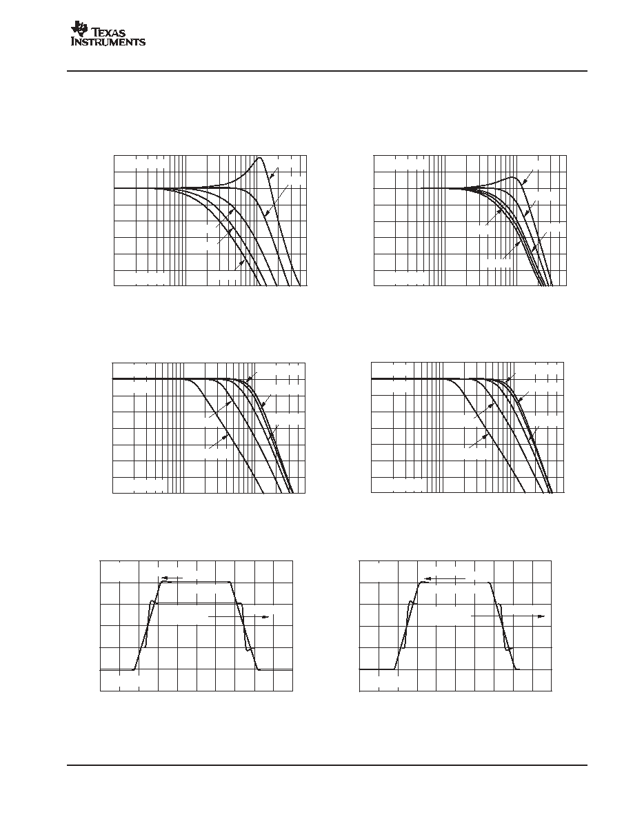
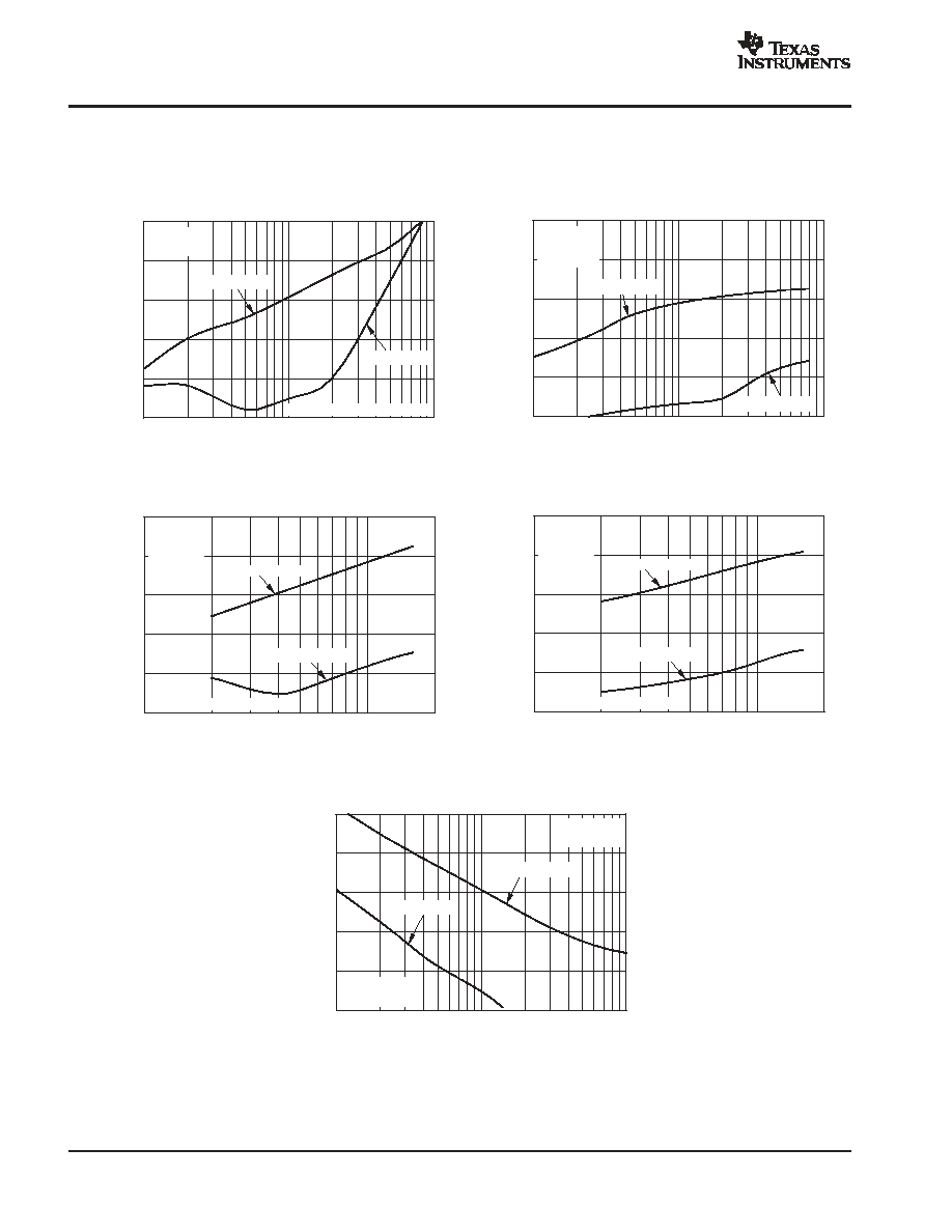
TYPICAL CHARACTERISTICS: V
S
=
±
6V
At TA = +25
∞
C, G = +4, RF = 453
, and RL = 100
, unless otherwise noted.
NONINVERTING SMALL-SIGNAL
FREQUENCY RESPONSE
Frequency (MHz)
1
10
100
500
6
3
0
-
3
-
6
-
9
-
12
-
15
-
18
N
o
r
m
al
i
z
ed
G
a
i
n
(
d
B
)
V
O
= 100mV
PP
See Figure 1
G = +2
G = +16
G = +12
G = +8
G = +4
INVERTING SMALL-SIGNAL
FREQUENCY RESPONSE
Frequency (MHz)
1
10
100
500
N
o
r
m
al
i
z
ed
G
a
i
n
(
d
B
)
6
3
0
-
3
-
6
-
9
-
12
-
15
-
18
G =
-
2
G =
-
4
G =
-
8
G =
-
16
G =
-
12
See Figure 2
V
O
= 100mV
PP
NONINVERTING LARGE-SIGNAL
FREQUENCY RESPONSE
Frequency (MHz)
1
10
100
500
Ga
i
n
(d
B
)
15
12
9
6
3
0
-
3
-
6
-
9
See Figure 1
V
O
= 100mV
PP
V
O
= 500mV
PP
V
O
= 2V
PP
G = +4V/V
R
L
= 100
V
O
= 5V
PP
V
O
= 1V
PP
INVERTING LARGE-SIGNAL
FREQUENCY RESPONSE
Frequency (MHz)
1
10
100
500
Ga
i
n
(
d
B
)
15
12
9
6
3
0
-
3
-
6
-
9
See Figure 4
V
O
= 100mV
PP
V
O
= 500mV
PP
V
O
= 2V
PP
V
O
= 5V
PP
V
O
= 1V
PP
See Figure 4
G =
-
4V/V
R
L
= 100
NONINVERTING PULSE RESPONSE
Time (20ns/div)
O
u
tp
ut
V
o
l
t
a
g
e
(
1V
/d
i
v
)
O
u
tput
V
o
l
t
age
(
1
0
0
mV
/
d
i
v
)
4V
PP
G = +4V/V
R
L
= 100
200mV
PP
Left Scale
Large Signal
Right Scale
Small Signal
See Figure 1
3
2
1
0
-
1
-
2
-
3
0.3
0.2
0.1
0
-
0.1
-
0.2
-
0.3
INVERTING PULSE RESPONSE
Time (20ns/div)
O
u
tput
V
o
l
t
a
g
e
(
1V
/
d
i
v
)
O
u
tpu
t
V
o
l
t
ag
e
(
1
00m
V
/
di
v
)
3
2
1
0
-
1
-
2
-
3
0.3
0.2
0.1
0
-
0.1
-
0.2
-
0.3
4V
PP
G =
-
4V/V
R
L
= 100
Left Scale
200mV
PP
Large Signal
Small Signal
Right Scale
See Figure 2
OPA2614
SBOS305A - JUNE 2004 - REVISED JANUARY 2005
www.ti.com
8
TYPICAL CHARACTERISTICS: V
S
=
±
6V (continued)
At TA = +25
∞
C, G = +4, RF = 453
, and RL = 100
, unless otherwise noted.
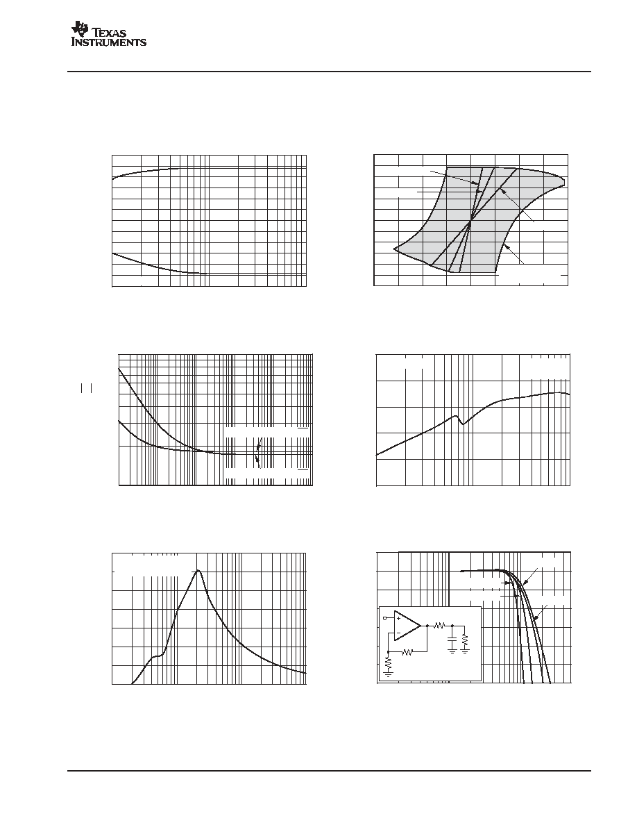
HARMONIC DISTORTION vs FREQUENCY
Frequency (MHz)
0.1
1
10
H
a
r
m
oni
c
D
i
s
to
r
t
i
o
n
(
d
B
c
)
-
60
-
70
-
80
-
90
-
100
-
110
Single Channel (see Figure 1)
G = +4
R
L
= 100
2nd-Harmonic
3rd-Harmonic
HARMONIC DISTORTION vs OUTPUT VOLTAGE
Output Voltage (V
PP
)
0.1
1
10
-
60
-
70
-
80
-
90
-
100
-
110
H
a
rm
o
n
i
c
D
i
s
t
o
rt
i
o
n
(
d
B
c)
G = +4
R
L
= 100
f = 1MHz
2nd-Harmonic
3rd-Harmonic
HARMONIC DISTORTION vs NONINVERTING GAIN
Gain Magnitude (V/V)
1
-
60
-
70
-
80
-
90
-
100
-
110
20
10
H
a
r
m
on
i
c
D
i
s
t
or
ti
on
(
d
B
c
)
2nd-Harmonic
3rd-Harmonic
Single Channel (see Figure 1)
V
O
= 2V
PP
f = 1MHz
R
L
= 100
HARMONIC DISTORTION vs INVERTING GAIN
Gain Magnitude (V/V)
1
-
60
-
70
-
80
-
90
-
100
-
110
20
10
H
a
r
m
on
i
c
D
i
s
t
or
ti
on
(
d
B
c
)
2nd-Harmonic
3rd-Harmonic
Single Channel (see Figure 2)
V
O
= 2V
PP
f = 1MHz
R
L
= 100
HARMONIC DISTORTION vs LOAD RESISTANCE
Load Resistance (
)
10
100
1000
-
60
-
70
-
80
-
90
-
100
-
110
H
a
rm
o
n
i
c
D
i
s
t
o
rt
i
o
n
(
d
B
c
)
Single Channel
(see Figure 1)
V
O
= 2V
PP
f = 1MHz
2nd-Harmonic
3rd-Harmonic
OPA2614
SBOS305A - JUNE 2004 - REVISED JANUARY 2005
www.ti.com
9
TYPICAL CHARACTERISTICS: V
S
=
±
6V (continued)
At TA = +25
∞
C, G = +4, RF = 453
, and RL = 100
, unless otherwise noted.
Load Resistance (
)
MAXIMUM OUTPUT SWING
vs LOAD RESISTANCE
10
6
5
4
3
2
1
0
-
1
-
2
-
3
-
4
-
5
-
6
100
1000
O
u
t
p
u
t
Vo
lt
a
g
e
(
V)
See Figure 1
OUTPUT VOLTAGE AND CURRENT LIMITATIONS
I
O
(mA)
-
400
6
5
4
3
2
1
0
-
1
-
2
-
3
-
4
-
5
-
6
0
100
200
300
-
200
-
100
-
300
400
V
O
(V
)
1W Internal Power
Single Channel
R
L
= 25
R
L
= 50
R
L
= 100
INPUT VOLTAGE AND CURRENT NOISE DENSITY
Frequency (Hz)
10
2
10
1
10
5
10
6
10
3
10
4
10
7
V
o
l
t
ag
e
N
oi
s
e
(
n
V
/
Hz
)
Cu
r
r
e
n
t
N
o
i
s
e
(
p
A
/
Hz
)
Voltage Noise 1.8nV/
Hz
Current Noise 1.7pA/
Hz
CHANNEL-TO-CHANNEL CROSSTALK
Frequency (MHz)
1
10
100
-
30
-
40
-
50
-
60
-
70
-
80
C
r
os
s
t
al
k
,
In
put
R
e
f
e
r
r
e
d
(
dB
)
Input-Referred
G = +4V/V
R
L
= 100
RECOMMENDED R
S
vs CAPACITIVE LOAD
Capacitive Load (pF)
1
10
100
1000
70
60
50
40
30
20
10
0
R
S
(
)
Gain of +4V/V
0dB Peaking Targeted
FREQUENCY RESPONSE vs CAPACITIVE LOAD
Frequency (MHz)
1
3
0
-
3
-
6
-
9
-
12
-
15
-
18
10
100
500
N
o
r
m
a
liz
e
d
G
a
in
t
o
C
a
p
a
ci
t
i
v
e
L
o
a
d
(
d
B
)
C
L
= 10pF
C
L
= 22pF
C
L
= 100pF
C
L
= 47pF
1/2
OPA2614
453
R
S
150
1k
C
L
1k
is optional.
OPA2614
SBOS305A - JUNE 2004 - REVISED JANUARY 2005
www.ti.com
10
TYPICAL CHARACTERISTICS: V
S
=
±
6V (continued)
At TA = +25
∞
C, G = +4, RF = 453
, and RL = 100
, unless otherwise noted.
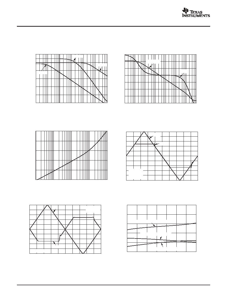
CMRR AND PSRR vs FREQUENCY
Frequency (Hz)
100
120
100
80
60
40
20
0
1k
10k
100k
1M
10M
100M
C
o
mmo
n-
Mod
e
R
e
j
e
c
t
i
o
n
R
at
i
o
(
d
B
)
Po
w
e
r
-
S
u
p
p
ly
R
e
j
e
c
t
io
n
R
a
t
io
(
d
B)
CMRR
-
PSRR
+PSRR
OPEN-LOOP GAIN AND PHASE
Frequency (Hz)
100
1k
10k
100k
1M
10M
100M
1G
120
100
80
60
40
20
0
-
20
O
pen-
Loo
p
G
ai
n
(
d
B
)
0
-
30
-
60
-
90
-
120
-
150
-
180
-
210
O
p
e
n
-
L
oop
P
h
a
s
e
(
_
)
A
OL
20 log (A
OL
)
CLOSED-LOOP OUTPUT IMPEDANCE
vs FREQUENCY
Frequency (Hz)
10k
100k
1M
10M
100M
10
1
0.1
0.01
0.001
0.0001
O
u
tput
Imped
anc
e
M
a
g
ni
tude
(
)
10
8
6
4
2
0
-
2
-
4
-
6
-
8
-
10
NONINVERTING OVERDRIVE RECOVERY
Time (100ns/div)
O
u
t
put
V
o
l
t
age
(
2
V
/
di
v
)
2.5
2.0
1.5
1.0
0.5
0
-
0.5
-
1.0
-
1.5
-
2.0
-
2.5
Inpu
t
V
o
l
tag
e
(
0
.5V
/
di
v
)
Output
G = +4V/V
R
L
= 100
See Figure 1
Input
10
8
6
4
2
0
-
2
-
4
-
6
-
8
-
10
2.5
2.0
1.5
1.0
0.5
0
-
0.5
-
1.0
-
1.5
-
2.0
-
2.5
INVERTING OVERDRIVE RECOVERY
Time (100ns/div)
O
u
t
p
u
t
V
o
l
t
ag
e
(
2V
/
d
i
v
)
Inp
u
t
V
o
l
ta
g
e
(
0
.5V
/
di
v
)
Input
See Figure 2
Output
G =
-
4V/V
R
L
= 100
TYPICAL DC DRIFT OVER TEMPERATURE
Ambient Temperature (
_
C)
-
50
0.5
0.3
0.1
-
0.1
-
0.3
-
0.5
-
25
0
25
50
75
100
125
In
put
O
ffs
et
V
o
l
t
a
g
e
(
m
V
)
10
5
0
-
5
-
10
In
pu
t
B
i
a
s
and
O
ffs
et
C
u
r
r
ent
(
µ
A)
Input Offset Voltage (V
IO
)
(10 Times Input Offset Current) 10 x I
OS
Input Bias Current (I
B
)

OPA2614
SBOS305A - JUNE 2004 - REVISED JANUARY 2005
www.ti.com
11
TYPICAL CHARACTERISTICS: V
S
=
±
6V (continued)
At TA = +25
∞
C, G = +4, RF = 453
, and RL = 100
, unless otherwise noted.
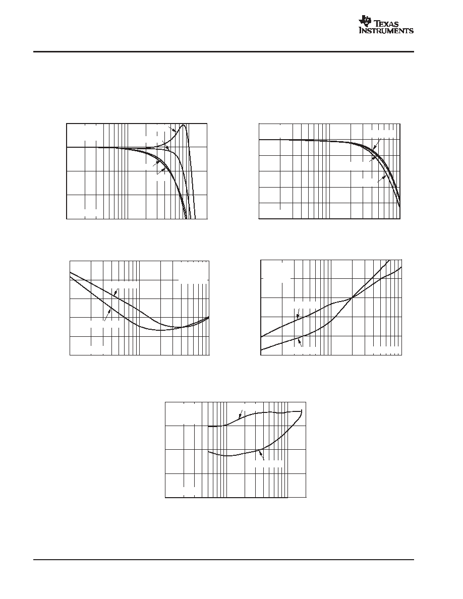
SUPPLY AND OUTPUT CURRENT vs TEMPERATURE
Ambient Temperature (
_
C)
-
50
300
290
280
270
260
250
-
25
0
25
50
75
100
125
O
u
t
put
C
u
r
r
en
t
(
1
0
mA
/di
v
)
12.3
12.2
12.1
12.0
11.9
11.8
S
u
pp
l
y
C
u
r
r
en
t
(
0
.
1m
A
/
d
i
v
)
Sourcing and Sinking Current
Left Scale
Supply Current
Right Scale
COMMON-MODE INPUT RANGE AND OUTPUT SWING
vs SUPPLY VOLTAGE
Supply Voltage (
±
V)
2.5
3.0
3.5
4.0
4.5
5.0
5.5
6
5
4
3
2
1
0
6
V
o
l
t
ag
e
R
an
ge
(
V
)
-
Output Voltage
-
V Input Voltage
+Output Voltage
+V Input Voltage
R
L
= 100
OPA2614
SBOS305A - JUNE 2004 - REVISED JANUARY 2005
www.ti.com
12
TYPICAL CHARACTERISTICS: V
S
=
±
6V, Differential Configuration
At TA = +25
∞
C, GD = 8, RF = 453
, and RL = 70
, unless otherwise noted. See Figure 5 for AC performance only.
DIFFERENTIAL SMALL-SIGNAL
FREQUENCY RESPONSE
Frequency (MHz)
1
3
0
-
3
-
6
-
9
200
100
10
N
o
r
m
al
i
z
ed
G
a
i
n
(
d
B
)
G
D
= +16
G
D
= +8
G
D
= +2
R
L
= 70
V
O
= 200mV
PP
See Figure 5
G
D
= +4
DIFFERENTIAL LARGE-SIGNAL
FREQUENCY RESPONSE
Frequency (MHz)
1
10
100
21
18
15
12
9
6
3
Ga
i
n
(d
B
)
V
O
= 5V
PP
V
O
= 2V
PP
V
O
= 0.5V
PP
See Figure 5
R
L
= 70
G
D
= +8
DIFFERENTIAL DISTORTION vs LOAD RESISTANCE
Load Resistance (
)
10
100
1k
-
60
-
70
-
80
-
90
-
100
-
110
H
a
rm
o
n
i
c
D
i
s
t
o
r
t
i
o
n
(d
B
c
)
See Figure 5
G
D
= +8
f = 1MHz
V
O
= 2V
PP
3rd-Harmonic
2nd-Harmonic
DIFFERENTIAL DISTORTION vs FREQUENCY
Frequency (MHz)
0.1
1
10
-
60
-
70
-
80
-
90
-
100
-
110
Ha
r
m
o
n
i
c
Di
s
t
o
r
ti
o
n
(
d
B
c
)
2nd-Harmonic
3rd-Harmonic
See Figure 5
G
D
= +8
R
L
= 70
V
O
= 2V
PP
DIFFERENTIAL DISTORTION
vs OUTPUT VOLTAGE
Output Voltage Swing (V
PP
)
0.1
-
80
-
85
-
90
-
95
-
100
20
10
1
Ha
r
m
o
n
i
c
Di
s
t
o
r
t
i
o
n
(
d
B
c
)
G
D
= +8V/V
R
L
= 70
f = 1MHz
See Figure 5
2nd-Harmonic
3rd-Harmonic
OPA2614
SBOS305A - JUNE 2004 - REVISED JANUARY 2005
www.ti.com
13
TYPICAL CHARACTERISTICS: V
S
= +5V
At TA = +25
∞
C, G = +4, RF = 453
, and RL = 100
, unless otherwise noted.
NONINVERTING SMALL-SIGNAL
FREQUENCY RESPONSE
Frequency (MHz)
1
10
100
500
9
6
3
0
-
3
-
6
-
9
N
o
r
m
al
i
z
ed
G
a
i
n
(
d
B
)
See Figure 3
G = +12V/V
G = +16V/V
G = +4V/V
G = +8V/V
G = +2V/V
V
O
= 100mV
PP
R
L
= 100
to V
S
/2
NONINVERTING SMALL-SIGNAL
FREQUENCY RESPONSE
Frequency (MHz)
1
10
100
500
9
6
3
0
-
3
-
6
-
9
N
o
rm
a
l
i
z
e
d
G
a
i
n
(d
B
)
G =
-
16V/V
G =
-
12V/V
G =
-
2V/V
G =
-
8V/V
G =
-
4V/V
See Figure 4
V
O
= 100mV
PP
R
L
= 100
to V
S
/2
NONINVERTING LARGE-SIGNAL
FREQUENCY RESPONSE
Frequency (MHz)
1
10
100
500
15
12
9
6
3
0
Ga
i
n
(d
B
)
V
O
= 2V
PP
V
O
= 1V
PP
V
O
= 0.1V
PP
G = +4V/V
R
L
= 100
to V
S
/2
V
O
= 0.5V
PP
See Figure 3
INVERTING LARGE-SIGNAL
FREQUENCY RESPONSE
Frequency (MHz)
1
10
100
500
15
12
9
6
3
0
Ga
i
n
(d
B
)
V
O
= 2V
PP
V
O
= 1V
PP
V
O
= 0.1V
PP
G =
-
4V/V
R
L
= 100
to V
S
/2
V
O
= 0.5V
PP
See Figure 4
NONINVERTING PULSE RESPONSE
Time (20ns/div)
O
u
tpu
t
V
o
l
t
ag
e
(
5
00mV
/
di
v
)
O
u
tpu
t
V
o
l
t
ag
e
(
1
00mV
/
di
v
)
4.5
4.1
3.7
3.3
2.9
2.5
2.1
1.7
1.3
0.9
0.5
3.0
2.9
2.8
2.7
2.6
2.5
2.4
2.3
2.2
2.1
2.0
2V
PP
G = +4V/V
R
L
= 100
to V
S
/2
200mV
PP
Left Scale
Large Signal
Right Scale
Small Signal
See Figure 3
INVERTING PULSE RESPONSE
Time (20ns/div)
O
u
t
p
ut
V
o
l
t
a
g
e
(
500
mV
/
d
i
v
)
O
u
t
p
ut
V
o
l
t
a
g
e
(
100
mV
/
d
i
v
)
4.5
4.1
3.7
3.3
2.9
2.5
2.1
1.7
1.3
0.9
0.5
3.0
2.9
2.8
2.7
2.6
2.5
2.4
2.3
2.2
2.1
2.0
2V
PP
G =
-
4V/V
R
L
= 100
to V
S
/2
200mV
PP
Left Scale
Large Signal
Right Scale
Small Signal

OPA2614
SBOS305A - JUNE 2004 - REVISED JANUARY 2005
www.ti.com
14
TYPICAL CHARACTERISTICS: V
S
= +5V (continued)
At TA = +25
∞
C, G = +4, RF = 453
, and RL = 100
, unless otherwise noted.
HARMONIC DISTORTION vs FREQUENCY
Frequency (MHz)
0.1
1
10
-
60
-
70
-
80
-
90
-
100
-
110
Ha
r
m
o
n
i
c
Di
s
t
o
r
ti
o
n
(
d
B
c
)
Single Channel
(see Figure 3)
V
O
= 2V
PP
G = +4
R
L
= 100
to V
S
/2
2nd-Harmonic
3rd-Harmonic
HARMONIC DISTORTION vs OUTPUT VOLTAGE
Output Voltage (V
PP
)
0.1
1
5
-
60
-
70
-
80
-
90
-
100
-
110
H
a
rm
o
n
i
c
D
i
s
t
o
rt
i
o
n
(
d
B
c
)
f = 1MHz
R
L
= 100
to V
S
/2
2nd-Harmonic
3rd-Harmonic
Single Channel
(see Figure 3)
HARMONIC DISTORTION vs NONINVERTING GAIN
Gain Magnitude (V/V)
1
20
10
-
60
-
70
-
80
-
90
-
100
-
110
Ha
r
m
o
n
i
c
Di
s
t
o
r
ti
o
n
(
d
B
c
)
2nd-Harmonic
3rd-Harmonic
V
O
= 2V
PP
f = 1MHz
R
L
= 100
to V
S
/2
HARMONIC DISTORTION vs INVERTING GAIN
Gain Magnitude (V/V)
1
20
10
-
60
-
70
-
80
-
90
-
100
-
110
Ha
r
m
o
n
i
c
Di
s
t
o
r
ti
o
n
(
d
B
c
)
V
O
= 2V
PP
f = 1MHz
R
L
= 100
to V
S
/2
2nd-Harmonic
3rd-Harmonic
HARMONIC DISTORTION vs LOAD RESISTANCE
Load Resistance (
)
10
100
1000
-
60
-
70
-
80
-
90
-
100
-
110
Ha
r
m
o
n
i
c
Di
s
t
o
r
ti
o
n
(
d
B
c
)
V
O
= 2V
PP
f = 1MHz
G = +4V/V
R
L
to V
S
/2
2nd-Harmonic
3rd-Harmonic

OPA2614
SBOS305A - JUNE 2004 - REVISED JANUARY 2005
www.ti.com
15
TYPICAL CHARACTERISTICS: V
S
= +5V, Differential Configuration
At TA = +25
∞
C, GD = 8, RF = 453
, and RL = 70
, unless otherwise noted.
R
G
0.01
µ
F
0.01
µ
F
0.01
µ
F
R
F
453
1/2
OPA2614
806
806
1/2
OPA2614
+5V
V
I
V
I
806
806
R
L
R
F
453
2R
F
R
G
G
D
= 1 +
DIFFERENTIAL SMALL-SIGNAL
FREQUENCY RESPONSE
Frequency (MHz)
0.1
10
200
100
6
3
0
-
3
-
6
-
9
N
o
r
m
a
l
iz
e
d
G
a
in
(
d
B)
R
L
= 70
G
D
= +2
G
D
= +4
G
D
= +8
G
D
= +16
DIFFERENTIAL LARGE-SIGNAL
FREQUENCY RESPONSE
Frequency (MHz)
1
200
100
10
Ga
i
n
(d
B
)
21
18
15
12
9
6
3
0
V
O
= 5V
PP
V
O
= 2V
PP
V
O
= 0.1V
PP
R
L
= 70
G
D
= 8V/V
DIFFERENTIAL DISTORTION vs LOAD RESISTANCE
Load Resistance (
)
10
100
1k
-
60
-
70
-
80
-
90
-
100
-
110
H
a
r
m
on
i
c
D
i
s
t
o
r
ti
on
(
d
B
c
)
G
D
= +8
V
O
= 2V
PP
f = 1MHz
3rd-Harmonic
2nd-Harmonic
DIFFERENTIAL DISTORTION vs FREQUENCY
Frequency (MHz)
0.1
1
10
-
60
-
70
-
80
-
90
-
100
-
110
H
a
r
m
on
i
c
D
i
s
t
or
ti
o
n
(
d
B
c
)
2nd-Harmonic
3rd-Harmonic
G
D
= 8V/V
R
L
= 70
V
O
= 2V
PP
DIFFERENTIAL DISTORTION vs OUTPUT VOLTAGE
Output Voltage Swing (V
PP
)
0.1
1
4
-
80
-
85
-
90
-
95
-
100
H
a
r
m
oni
c
D
i
s
tor
t
i
o
n
(
dB
c
)
G
D
= +8V/V
R
L
= 70
f = 1MHz
2nd-Harmonic
3rd-Harmonic
OPA2614
SBOS305A - JUNE 2004 - REVISED JANUARY 2005
www.ti.com
16
APPLICATION INFORMATION
WIDEBAND VOLTAGE-FEEDBACK OPERATION
The OPA2614 gives the exceptional AC performance of a
wideband voltage-feedback op amp with a highly linear,
high-power output stage. Requiring only 6mA/ch
quiescent current, the OPA2614 swings to within 1.0V of
either supply rail and delivers in excess of 280mA at room
temperature. This low-output headroom requirement,
along with supply voltage independent biasing, gives
remarkable single (+5V) supply operation. The OPA2614
delivers greater than 40MHz bandwidth driving a 2V
PP
output into 100
on a single +5V supply. Previous boosted
output stage amplifiers typically suffer from very poor
crossover distortion as the output current goes through
zero. The OPA2614 achieves exceptional power gain with
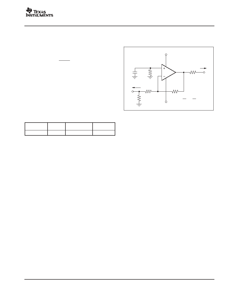
much better linearity. Figure 1 shows the DC-coupled,
gain of +4, dual power-supply circuit configuration used as
the basis of the
±
6V Electrical and Typical Characteristics.
For test purposes, the input impedance is set to 50
with
a resistor to ground, and the output impedance is set to
50
with a series output resistor. Voltage swings reported
in the electrical characteristics are taken directly at the
input and output pins, whereas load powers (dBm) are
defined at a matched 50
load. For the circuit of Figure 1,
the total effective load is 100
|| 603
= 86
.
1/2
OPA2614
+6V
+
-
6V
50
Load
50
50
V
O
V
I
50
Source
R
G
150
R
F
453
+
6.8
µ
F
0.1
µ
F
6.8
µ
F
0.1
µ
F
+V
S
-
V
S
Figure 1. DC-Coupled, G = +4, Bipolar Supply,
Specification and Test Circuit
Figure 2 shows the DC-coupled, bipolar supply circuit
configuration used as the basis for the Inverting Gain
-4V/V Typical Characteristics. Key design considerations
of the inverting configuration are developed in the Inverting
Amplifier Operation section.
1/2
OPA2614
+5V
-
5V
50
Load
50
V
O
V
I
50
Source
R
M
89
R
F
453
R
G
113
Power-supply
decoupling
not shown.
208
Figure 2. DC-Coupled, G = -4, Bipolar Supply,
Specification and Test Circuit
Figure 3 shows the AC-coupled, gain of +4, single-supply
circuit configuration used as the basis of the +5V Electrical
and Typical Characteristics. Though not a rail-to-rail
design, the OPA2614 requires minimal input and output
voltage headroom compared to other very wideband
voltage-feedback op amps. It will deliver a 2.6V
PP
output
swing on a single +5V supply with greater than 20MHz
bandwidth. The key requirement of broadband single-
supply operation is to maintain input and output signal
swings within the usable voltage ranges at both the input
and the output. The circuit of Figure 3 establishes an input
midpoint bias using a simple resistive divider from the +5V
supply (two 906
resistors). The input signal is then
AC-coupled into this midpoint voltage bias. The input
voltage can swing to within 1.4V of either supply pin, giving
a 2.2V
PP
input signal range centered between the supply
pins. The input impedance matching resistor (56.2
) used
for testing is adjusted to give a 50
input match when the
parallel combination of the biasing divider network is
included. The gain resistor (R
G
) is AC-coupled, giving the
circuit a DC gain of +1
which puts the input DC bias
voltage (2.5V) on the output as well. Again, on a single +5V
supply, the output voltage can swing to within 1.1V of either
supply pin while delivering more than 100mA output
current. A demanding 100
load to a midpoint bias is used
in this characterization circuit. The new output stage used
in the OPA2614 can deliver large bipolar output currents
into this midpoint load with minimal crossover distortion,
as shown by the +5V supply, harmonic distortion plots.

OPA2614
SBOS305A - JUNE 2004 - REVISED JANUARY 2005
www.ti.com
17
1/2
OPA2614
+5V
+V
S
V
S
/2
906
100
V
O
V
I
56.2
906
R
F
453
R
G
150
0.1
µ
F
0.1
µ
F
6.8
µ
F
+
0.1
µ
F
Figure 3. AC-Coupled, G = +4, Single-Supply,
Specification and Test Circuit
The last configuration used as the basis of the +5V
Electrical and Typical Characteristics is shown in Figure 4.
Design considerations for this inverting, bipolar supply
configuration are covered either in single-supply
configuration (as shown in Figure 3) or in the Inverting
Amplifier Operation section.
1/2
OPA2614
+5V
V
S
/2
906
V
I
100
V
O
906
R
F
453
R
M
89
6.8
µ
F
+
0.1
µ
F
0.1
µ
F
0.1
µ
F
R
G
113
Figure 4. AC-Coupled, G = -4, Single-Supply,
Specification and Test Circuit
DIFFERENTIAL INTERFACE APPLICATIONS
Dual op amps are particularly suitable to differential input
to differential output applications. Typically, these fall into
either Analog-to-Digital Converter (ADC) input interface or
line driver applications. Two basic approaches to
differential I/O are noninverting or inverting configurations.
Since the output is differential, the signal polarity is
somewhat meaningless--the noninverting and inverting
terminology applies here to where the input is brought into
the OPA2614. Each has its advantages and disadvan-
tages. Figure 5 shows a basic starting point for
noninverting input differential I/O applications.
R
F
453
R
F
453
1/2
OPA2614
+V
CC
Power-supply
decoupling not
shown.
-
V
CC
R
G
301
V
O
1/2
OPA2614
V
I
Figure 5. Noninverting Differential I/O Amplifier
This approach provides for a source termination
impedance that is independent of the signal gain. For
instance, simple differential filters may be included in the
signal path right up to the noninverting inputs without
interacting with the gain setting. The differential signal gain
for the circuit of Figure 5 is:
A
D
+
1
)
2
R
F
R
G
Since the OPA2614 is a voltage-feedback (VFB) amplifier,
its bandwidth is principally controlled by the noise gain.
The equivalent noise gain for Figure 5 is:
1
)
2
453
W
301
W +
4V V
Various combinations of single-supply or AC-coupled gain
can also be delivered using the basic circuit of Figure 5.
Common-mode bias voltages on the two noninverting
inputs pass on to the output with a gain of 1 since an equal
DC voltage at each inverting node creates no current
through R
G
. This circuit does show a common-mode gain
of 1 from input to output. The source connection should
either remove this common-mode signal if undesired
(using an input transformer can provide this function), or
the common-mode voltage at the inputs can be used to set
the output common-mode bias. If the low common-mode
rejection of this circuit is a problem, the output interface
may also be used to reject that common-mode. For
instance, most modern differential input ADCs reject
common-mode signals very well, while a line driver
application through a transformer will also remove the
common-mode signal through to the line.
(1)
(2)

OPA2614
SBOS305A - JUNE 2004 - REVISED JANUARY 2005
www.ti.com
18
OPA2614 vs OPA2613 PERFORMANCE
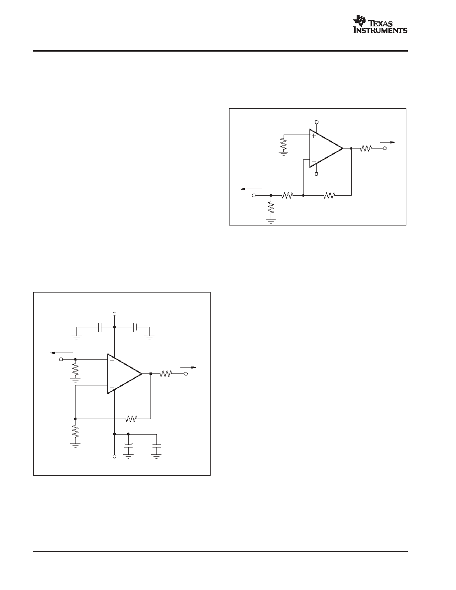
The OPA2614 is a de-compensated version of the unity
gain stable OPA2613. This decompensation gives a flat
response at a gain of +4, higher gain bandwidth product,
and twice the slew rate of the OPA2613. The OPA2614
should not be used for integrator-based active filters as
unity gain stability is required for the correct operation of
that filter type. It can be used for Sallen-Key type filters
where the filter is implemented using a simple gain
stage--as long as that gain is
2 when using the
OPA2614.
The higher slew rate of the OPA2614 (145V/
µ
s vs 70V/
µ
s
for the OPA2613) will give a higher full-power bandwidth
and lower distortion to higher output swings. For example,
comparing the
±
6V differential plots for the OPA2613 to
those of the OPA2614, we see about twice the large signal
bandwidth for the OPA2614. This is also operating at twice
the signal gain, but since the gain bandwidth for the
OPA2614 is approximately twice that of the OPA2613, this
is as expected.
DIFFERENTIAL LARGE-SIGNAL
FREQUENCY RESPONSE
Frequency (MHz)
1
10
100
15
12
9
6
3
0
Ga
i
n
(d
B
)
V
O
= 5V
PP
V
O
= 2V
PP
V
O
= 0.2V
PP
R
L
= 70
G
D
= +4
V
O
= 1V
PP
Figure 6. OPA2613 Differential Gain of +4
Large-Signal Bandwidth
DIFFERENTIAL LARGE-SIGNAL
FREQUENCY RESPONSE
Frequency (MHz)
1
10
100
21
18
15
12
9
6
3
Ga
i
n
(d
B
)
V
O
= 5V
PP
V
O
= 2V
PP
V
O
= 0.5V
PP
R
L
= 70
G
D
= +8
Figure 7. OPA2614 Differential Gain of +8
Large-Signal Bandwidth
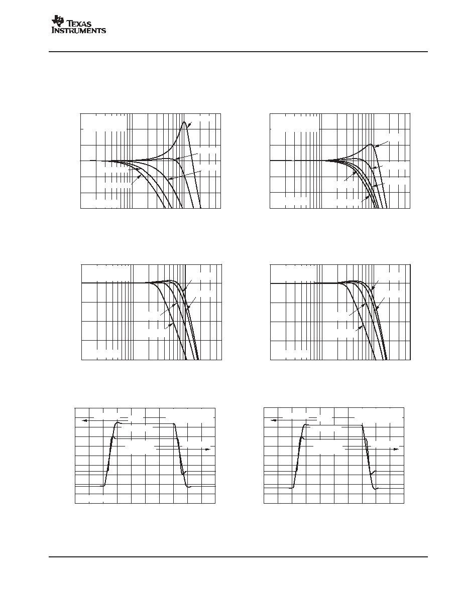
The increased slew rate of the OPA2614 over the
OPA2613 will also give lower distortion at higher output
swings and/or frequency. Figure 8 and Figure 9 show the
differential test data for the OPA2613 and OPA2614,
repectively.
DIFFERENTIAL DISTORTION
vs OUTPUT VOLTAGE
Output Voltage Swing (V
PP
)
0.1
-
70
-
75
-
80
-
85
-
90
-
95
-
100
-
105
20
10
1
H
a
r
m
oni
c
D
i
s
to
r
t
i
o
n
(
dB
c
)
G
D
= 4
R
L
= 70
f = 1MHz
2nd-Harmonic
3rd-Harmonic
Figure 8. OPA2613 Differential Gain of +4
Distortion vs Output at 1MHz
DIFFERENTIAL DISTORTION
vs OUTPUT VOLTAGE
Output Voltage Swing (V
PP
)
0.1
-
80
-
85
-
90
-
95
-
100
20
10
1
Ha
r
m
o
n
i
c
Di
s
t
o
r
t
i
o
n
(
d
B
c
)
G
D
= +8V/V
R
L
= 70
f = 1MHz
2nd-Harmonic
3rd-Harmonic
Figure 9. OPA2614 Differential Gain of +8
Distortion vs Output at 1MHz
Notice how much lower the 3rd-harmonic is above 10V
PP
for the OPA2614 vs the OPA2613. These test conditions
were set up to have the same loop gain so the difference
in high output 3rd-harmonics can be attributed principally
to the high slew rate for the OPA2614.
These differences show that the OPA2614 would be
preferred for higher gains, higher frequency applications
over the OPA2613 while the OPA2613 would be preferred
where unity gain stability is required in the application.
OPA2614
SBOS305A - JUNE 2004 - REVISED JANUARY 2005
www.ti.com
19
SINGLE-SUPPLY ADSL UPSTREAM DRIVER
Figure 10 shows an example of a single-supply ADSL
upstream driver. The dual OPA2614 is configured as a
differential gain stage to provide signal drive to the primary
of the transformer (here, a step-up transformer with a turns
ratio of 1:2). The main advantage of this configuration is
the cancellation of all even harmonic distortion products.
Another important advantage for ADSL applications is that
each amplifier needs only to swing half of the total output
required driving the load.
R
G
308
1k
1k
1
µ
F
0.1
µ
F
0.1
µ
F
R
M
12.5
100
Z
LINE
AFE
2V
PP
Max
Assumed
R
F
1k
20
20
R
F
1k
1/2
OPA2614
1/2
OPA2614
+12V
1:2
15V
PP
I
P
= 150mA
I
P
= 150mA
R
M
12.5
+6.3V
Figure 10. Single-Supply ADSL Upstream Driver
The analog front-end (AFE) signal is AC-coupled to the
driver, and the noninverting input of each amplifier is
biased slightly above the mid-supply voltage (+6.3V in this
case). In addition to providing the proper biasing to the
amplifier, this approach also provides a high-pass filtering
with a corner frequency, set here at 1.6kHz. As the
upstream signal bandwidth starts at 26kHz, this high-pass
filter does not generate any problems and has the
advantage of filtering out unwanted lower frequencies.
The input signal is amplified with a gain set by the following
equation:
G
D
+
1
)
2
R
F
R
G
With R
F
= 1k
and R
G
= 308
, the gain for this differential
amplifier is 7.5. This gain boosts the AFE signal, assumed
to be a maximum of 2V
PP
, to a maximum of 15V
PP
.
The two back-termination resistors (12.5
each) added at
each input of the transformer make the impedance of the
modem match the impedance of the phone line, and also
provide a means of detecting the received signal for the
receiver. The value of these resistors (R
M
) is a function of
the line impedance and the transformer turns ratio (n),
given by the following equation:
R
M
+
Z
LINE
2n
2
LINE DRIVER HEADROOM MODEL
The first step in a transformer-coupled, twisted-pair driver
design is to compute the peak-to-peak output voltage from
the target specifications. This is done using the following
equations:
P
L
+
10
log
V
RMS
2
(1mW)
R
L
With P
L
power and V
RMS
voltage at the load, and R
L
line
impedance, this gives the following:
V
RMS
+
(1mW)
R
L
10
P
L
10
V
P
+
Crest Factor
V
RMS
+
CF
V
RMS
with V
P
equal to the peak voltage at the load and CF as the
Crest Factor.
V
LPP
+
2
CF
V
RMS
with V
LPP
as the peak-to-peak voltage at the load.
Consolidating Equations 4 through 7 allows expressing
the required peak-to-peak voltage at the load as a function
of the crest factor, the load impedance, and the power at
the load. Thus:
V
LPP
+
2
CF
(1mW)
R
L
10
P
L
10
This V
LPP
is usually computed for a nominal line
impedance and may be taken as a fixed design target.
The next step for the driver is to compute the individual
amplifier output voltage and currents as a function of V
PP
on the line and transformer turns ratio. As the turns ratio
changes, the minimum allowed supply voltage changes
along with it. The peak current (I
P
) in the amplifier output
is given by:
"
I
P
+
1
2
2
V
LPP
n
1
4R
M
(3)
(4)
(5)
(6)
(7)
(8)
(9)
(10)
OPA2614
SBOS305A - JUNE 2004 - REVISED JANUARY 2005
www.ti.com
20
With V
LPP
as defined in Equation 8, and R
M
as defined in
Equation 4 and shown in Figure 11.
R
M
R
M
V
Lpp
n
V
Lpp
R
L
2V
Lpp
n
V
pp
=
1:n
Figure 11. Driver Peak Output Voltage
With the previous information available, it is now possible
to select a supply voltage and the turns ratio desired for the
transformer as well as calculate the headroom for the
OPA2614.
The model (shown in Figure 12) can be described with the
following set of equations:
1.
First, as available output swing:
V
PP
+
V
CC
*
(V
1
)
V
2
)
*
I
P
(R
1
)
R
2
)
2.
Or as required supply voltage:
V
CC
+
V
PP
)
(V
1
)
V
2
)
)
I
P
(R
1
)
R
2
)
The minimum supply voltage for a power and load
requirement is given by Equation 11.
V
O
R
1
V
1
+V
CC
R
2
V
2
I
P
Figure 12. Line Driver Headroom Model
V
1
, V
2
, R
1
, and R
2
are given in Table 1 for both +12V and
+5V operation.
Table 1. Line Driver Headroom Model Values
V1
R1
V2
R2
+5V
1.0V
2
1.0V
5.5
+12V
1.0V
2
1.0V
5.5
TOTAL DRIVER POWER FOR xDSL
APPLICATIONS
The total internal power dissipation for the OPA2614 in an
xDSL line driver application will be the sum of the
quiescent power and the output stage power. The
OPA2614 holds a relatively constant quiescent current
versus supply voltage--giving a power contribution that is
simply the quiescent current times the supply voltage used
(the supply voltage will be greater than the solution given
in Equation 12). The total output stage power may be
computed with reference to Figure 13.
R
T
+V
CC
I
AVG
=
I
P
C
F
Figure 13. Output Stage Power Model
The two output stages used to drive the load of Figure 11
can be seen as an H-Bridge in Figure 13. The average
current drawn from the supply into this H-Bridge and load
will be the peak current in the load given by Equation 10
divided by the crest factor (CF) for the xDSL modulation.
This total power from the supply is then reduced by the
power in R
T
to leave the power dissipated internal to the
drivers in the four output stage transistors. That power is
simply the target line power used in Equation 5 plus the
power lost in the matching elements (R
M
). In the examples
here, a perfect match is targeted, giving the same power
in the matching elements as in the load. The output stage
power is then set by Equation 13.
P
OUT
+
I
P
CF
V
CC
*
2P
L
The total amplifier power is then:
P
TOT
+
I
q
V
CC
)
I
P
CF
V
CC
*
2P
L
(11)
(12)
(13)
(14)
OPA2614
SBOS305A - JUNE 2004 - REVISED JANUARY 2005
www.ti.com
21
For the ADSL CPE upstream driver design of Figure 10,
the peak current is 150mA for a signal that requires a crest
factor of 5.33 with a target line power of 13dBm into 100
(20mW). With a typical quiescent current of 12mA and a
nominal supply voltage of +12V, the total internal power
dissipation for the solution of Figure 10 will be:
P
TOT
+
12mA(12V)
)
150mA
5.33
(12V)
*
2(20mW)
+
400mW
DESIGN-IN TOOLS
DEMONSTRATION BOARDS
A PC board is available to assist in the initial evaluation of
circuit performance using the OPA2614 in its two package
styles. It is available, free, as an unpopulated PC board
delivered with descriptive documentation. The summary
information for this unit is shown in Table 2.
Check the TI web site (www.ti.com) to request this board.
Table 2. Demonstration Board Ordering
Information
PRODUCT
PACKAGE
DEMO BOARD
NUMBER
ORDERING
NUMBER
OPA2614ID
SO-8
DEM
-
OPA268XU
SBOU003
MACROMODELS AND APPLICATIONS
SUPPORT
Computer simulation of circuit performance using SPICE
is often useful when analyzing the performance of analog
circuits and systems. This is particularly true for video and
RF amplifier circuits where parasitic capacitance and
inductance can have a major effect on circuit performance.
A SPICE model for the OPA2614 is available through the
TI web site (www.ti.com). This model does a good job of
predicting small-signal AC and transient performance
under a wide variety of operating conditions, but does not
do as well in predicting the harmonic distortion or video
d
G
/d
P
characteristics. This model does not attempt to
distinguish between the package types in small-signal AC
performance, nor does it attempt to simulate channel-to-
channel coupling.
INVERTING AMPLIFIER OPERATION
As the OPA2614 is a general-purpose, wideband
voltage-feedback op amp, most of the familiar op amp
application circuits are available to the designer.
Wideband inverting operation is particularly suited to the
OPA2614. Figure 14 shows a typical inverting
configuration where the I/O impedances and signal gain
from Figure 1 are retained in an inverting circuit
configuration.
1/2
OPA2614
R
F
453
V
O
V
I
R
G
113
+6V
-
6V
50
50
Load
V
O
Power-supply
decoupling not
shown.
V
I
50
Source
R
M
89
110
0.01
µ
F
R
F
R
G
=
-
=
-
4
Figure 14. Inverting Gain of -4 with Impedance
Matching
In the inverting configuration, two key design
considerations must be noted. The first is that the gain
resistor (R
G
) becomes part of the input impedance. If input
impedance matching is desired (which is beneficial
whenever the signal is coupled through a cable, twisted-
pair, long PC board trace, or other transmission line
conductor), it is normally necessary to add an additional
matching resistor to ground. R
G
, by itself, is not normally
set to the required input impedance since its value, along
with the desired gain, will determine an R
F
, which may be
non-optimal from a frequency response standpoint. The
total input impedance for the source becomes the parallel
combination of R
G
and R
M
.
The second major consideration, touched on in the
previous paragraph, is that the signal source impedance
becomes part of the noise gain equation and has an effect
on the bandwidth. In the example of Figure 14, the R
M
value combines in parallel with the external 50
source
impedance, yielding an effective driving impedance of
50
|| 89
= 32
. This impedance is added in series with
R
G
for calculating the noise gain
which gives NG = 4.12.
Note that the noninverting input in this bipolar supply
inverting application is connected to ground through a
110
resistor. It is often suggested that an additional
resistor be connected to ground on the noninverting input
to achieve bias current error cancellation at the output.
(15)
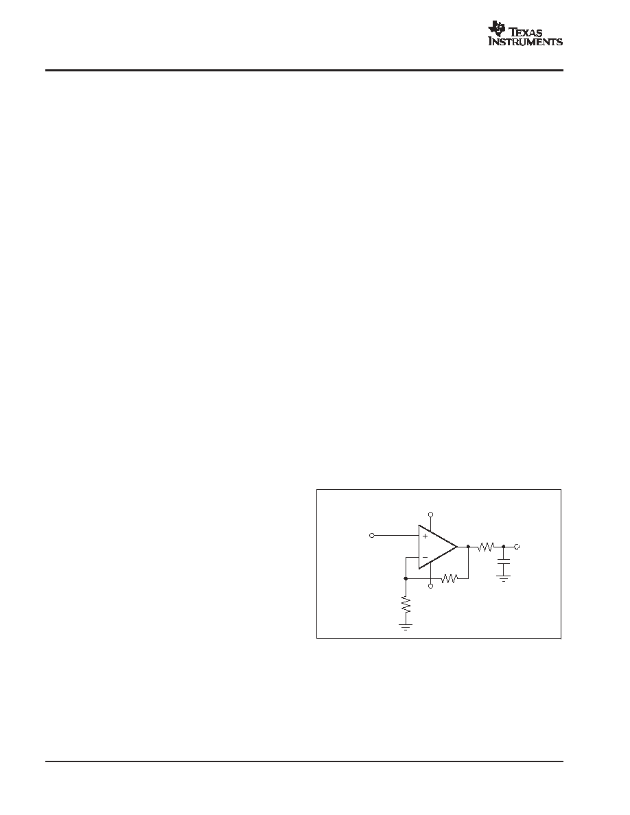
OPA2614
SBOS305A - JUNE 2004 - REVISED JANUARY 2005
www.ti.com
22
OUTPUT CURRENT AND VOLTAGE
The OPA2614 provides output voltage and current
capabilities that are unsurpassed in a low-cost dual
monolithic op amp. Under no-load conditions at +25
∞
C, the
output voltage typically swings closer than 1V to either
supply rail; tested at +25
∞
C, swing limit is within 1.1V of
either rail. Into a 12
load (the minimum tested load), it
delivers more than
±
280mA continuous output current.
The specifications described previously, though familiar in
the industry, consider voltage and current limits separately.
In many applications, it is the voltage times current (or V-I
product) that is more relevant to circuit operation. Refer to
the Output Voltage and Current Limitations plot in the
Typical Characteristics. The X and Y axes of this graph
show the zero-voltage output current limit and the
zero-current output voltage limit, respectively. The four
quadrants give a more detailed view of the OPA2614
output drive capabilities, noting that the graph is bounded
by a safe operating area of 1W maximum internal power
dissipation (in this case, for one channel only).
Superimposing resistor load lines onto the plot shows that
the OPA2614 can drive +4.8 and -4.1 into 25
without
exceeding the output capabilities or the 1W dissipation
limit. A 100
load line (the standard test circuit load)
shows the full
±
4.9V output swing capability, as shown in
the Electrical Characteristics tables. The minimum
specified output voltage and current over temperature are
set by worst-case simulations at the cold temperature
extreme. Only at cold startup will the output current and
voltage decrease to the numbers shown in the Electrical
Characteristics tables. As the output transistors deliver
power, the junction temperatures increase, decreasing the
V
BE
s (increasing the available output voltage swing), and
increasing the current gains (increasing the available
output current). In steady-state operation, the available
output voltage and current will always be greater than that
shown in the over-temperature specifications, since the
output stage junction temperatures will be higher than the
minimum specified operating ambient.
DRIVING CAPACITIVE LOADS
One of the most demanding and yet very common load
conditions for an op amp is capacitive loading. Often, the
capacitive load is the input of an ADC
including
additional external capacitance that may be recom-
mended to improve the ADC linearity. A high-speed, high
open-loop gain amplifier like the OPA2614 can be very
susceptible to decreased stability and closed-loop
response peaking when a capacitive load is placed directly
on the output pin. When the amplifier open-loop output
resistance is considered, this capacitive load introduces
an additional pole in the signal path that can decrease the
phase margin. Several external solutions to this problem
have been suggested.
When the primary considerations are frequency response
flatness, pulse response fidelity, and/or distortion, the
simplest and most effective solution is to isolate the
capacitive load from the feedback loop by inserting a
series isolation resistor between the amplifier output and
the capacitive load. This does not eliminate the pole from
the loop response, but rather shifts it and adds a zero at a
higher frequency. The additional zero acts to cancel the
phase lag from the capacitive load pole, thus increasing
the phase margin and improving stability. The Typical
Characteristics show the Recommended R
S
vs Capacitive
Load and the resulting frequency response at the load.
Parasitic capacitive loads greater than 2pF can begin to
degrade the performance of the OPA2614. Long PC board
traces, unmatched cables, and connections to multiple
devices can easily cause this value to be exceeded.
Always consider this effect carefully, and add the
recommended series resistor as close as possible to the
OPA2614 output pin (see the Board Layout Guidelines
section).
The very high output current and low gain stability for the
OPA2614 can be used to drive large capacitive loads with
moderate slew rates. An example is shown in Figure 15,
where a 2000pF load cap is driven with a 2MHz square
wave to give a
±
5V swing. The supplies were slightly
increased to give more headroom for the charging current
through the 2
isolation resistor.
1/2
OPA2614
453
+6.2V
Supply decoupling
not shown.
-
6.2V
2
113
V
O
2000pF
±
1.25V
2MHz
V
I
Square
Wave
Input
Figure 15. Large Capacitive Load Driver
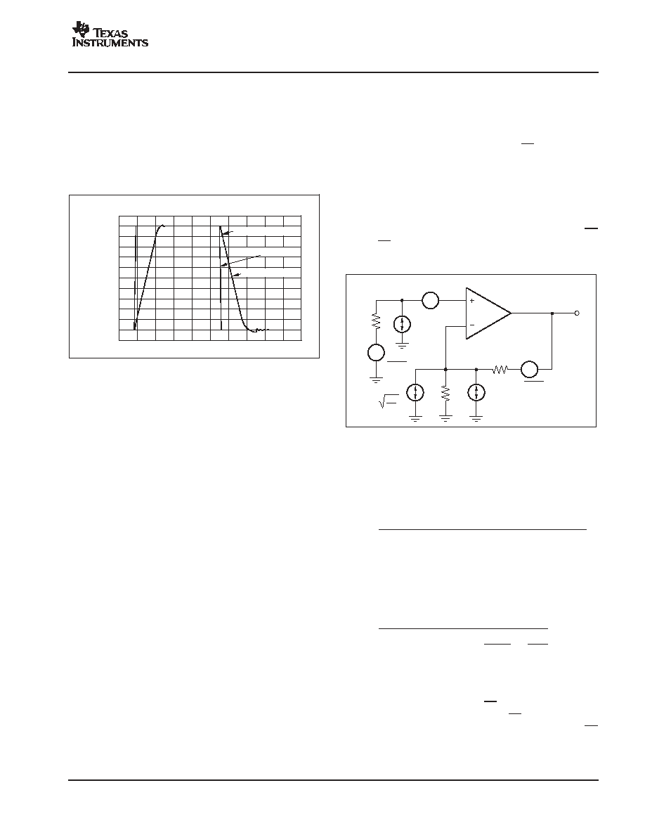
OPA2614
SBOS305A - JUNE 2004 - REVISED JANUARY 2005
www.ti.com
23
Figure 16 shows a comparison of 4
∑
Input voltage to the
capacitor voltage. The transition time is set by the 145V/
µ
s
slew rate for the OPA2614. For this controlled dV/dT, the
charging current into the 2000pF load will be given by:
Slew Rate = I
P
/C
Solving for I
P
gives:
I
P
+
2000pF
145V
m
s
+
290mA peak current
LARGE-SIGNAL CAPACITIVE LOAD DRIVE
Time (50ns/div)
Inpu
t
a
n
d
O
u
tput
V
o
l
t
age
Capacitor Voltage
4X Input Voltage
145V/
µ
s Slew Rate
6
5
4
3
2
1
0
-
1
-
2
-
3
-
4
-
5
-
6
Figure 16. Large-Signal Capacitive Load Drive
At these larger capacitive loads, very low series R will
maintain stability
but some R is always required.
DISTORTION PERFORMANCE
The OPA2614 provides good distortion performance into
a 100
load on
±
6V supplies. Generally, until the
fundamental signal reaches high frequency or power
levels, the 2nd-harmonic dominates the distortion with a
negligible 3rd-harmonic component. Focusing then on the
2nd-harmonic, increasing the load impedance improves
distortion directly. Remember that the total load includes
the feedback network
in the noninverting configuration
(see Figure 1), this is the sum of R
F
+ R
G
, whereas in the
inverting configuration, it is just R
F
. Also, providing an
additional supply decoupling capacitor (0.01
µ
F) between
the supply pins (for bipolar operation) improves the
2nd-order distortion slightly (3dB to 6dB).
In most op amps, increasing the output voltage swing
increases harmonic distortion directly. The Typical
Characteristics show the 2nd-harmonic increasing at a
little less than the expected 2x rate whereas the
3rd-harmonic increases at a little less than the expected 3x
rate. Where the test power doubles, the difference
between it and the 2nd-harmonic decreases less than the
expected 6dB, whereas the difference between it and the
3rd-harmonic decreases by less than the expected 12dB.
Operating differentially will suppress the 2nd-order
harmonics below the 3rd.
Operating as a differential I/O stage will also suppress the
2nd-harmonic distortion.
NOISE PERFORMANCE
Wideband voltage-feedback op amps generally have a
lower output noise than comparable current-feedback op
amps. The OPA2614 offers an excellent balance between
voltage and current noise terms to achieve low output
noise. The input voltage noise (1.8nV/
Hz) is lower than
most low-gain stable, wideband voltage-feedback op
amps. The op amp input voltage noise and the two input
current noise terms combine to give low output noise
under a wide variety of operating conditions. Figure 17
shows the op amp noise analysis model with all the noise
terms included. In this model, all noise terms are taken to
be noise voltage or current density terms in either nV/
Hz
or pA/
Hz.
4kT
R
G
R
G
R
F
R
S
1/2
OPA2614
I
BI
E
O
I
BN
4kT = 1.6E
-
20J
at 290
_
K
E
RS
E
NI
4
kTR
S
4kTR
F
Figure 17. Op Amp Noise Analysis Model
The total output spot noise voltage can be computed as the
square root of the sum of all squared output noise voltage
contributors. Equation 17 shows the general form for the
output noise voltage using the terms given in Figure 17.
E
O
+
ENI
2
)
IBN
R
S
2
)
4kTR
S
NG2
)
IBI
RF
2
)
4kTRFNG
Dividing this expression by the noise gain (NG = (1 + R
F
/R
G
))
gives the equivalent input-referred spot noise voltage at the
noninverting input, as shown in Equation 18.
E
N
+
E
NI
2
)
I
BN
R
S
2
)
4kTR
S
)
I
BI
R
F
NG
2
)
4kTR
F
NG
Evaluating these two equations for the OPA2614 circuit
and component values (see Figure 1) gives a total output
spot noise voltage of 6.34nV/
Hz and a total equivalent
input spot noise voltage of 3.2nV/
Hz. This total input
referred spot noise voltage is higher than the 1.8nV/
Hz
specification for the op amp voltage noise alone. This
reflects the noise added to the output by the inverting
current noise times the feedback resistor.
(16)
(17)
(18)
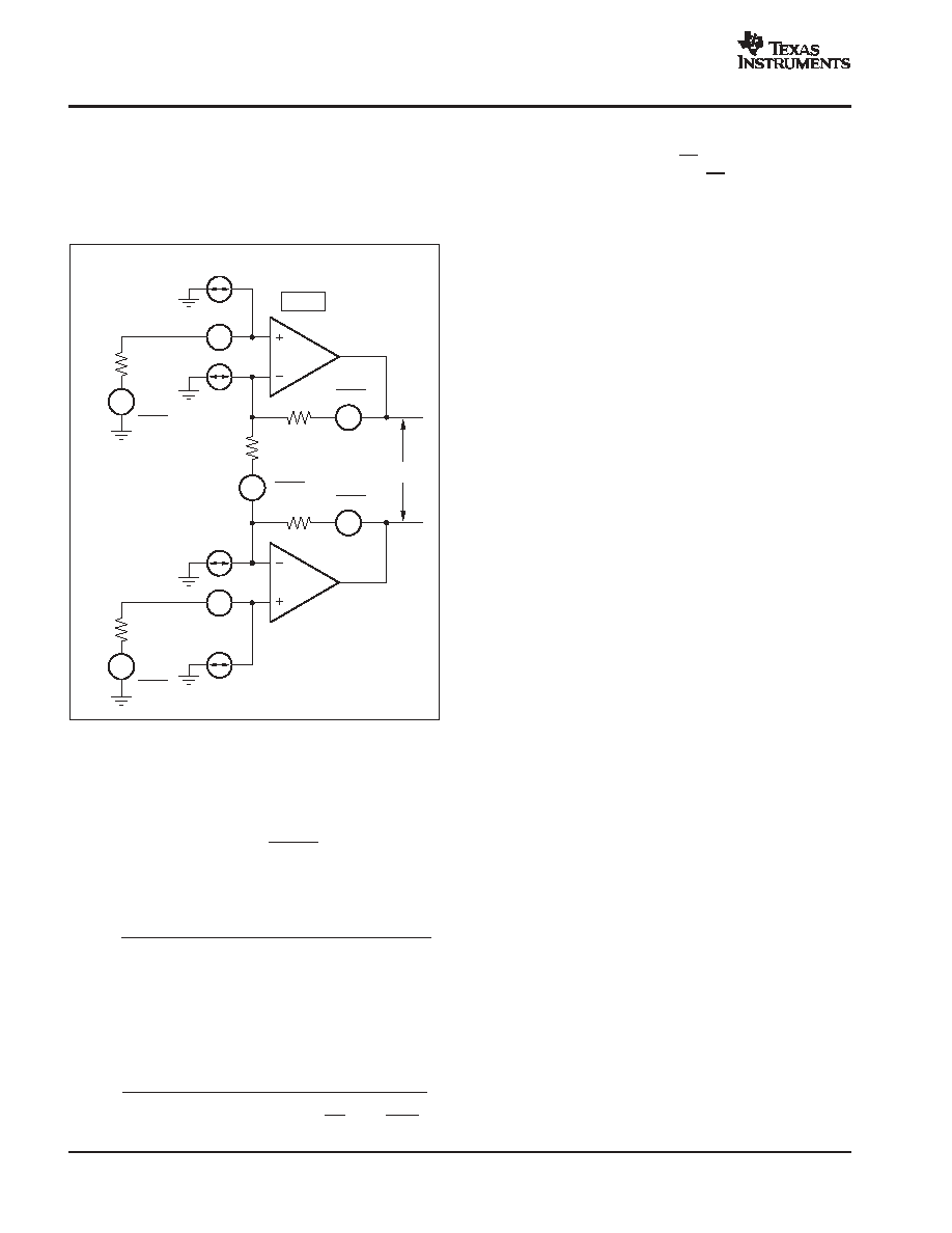
OPA2614
SBOS305A - JUNE 2004 - REVISED JANUARY 2005
www.ti.com
24
DIFFERENTIAL NOISE PERFORMANCE
Because the OPA2614 is used as a differential driver in
xDSL applications, it is important to analyze the noise in
such a configuration. Figure 18 shows the op amp noise
model for the differential configuration.
R
G
R
F
R
S
E
O
2
Driver
E
RS
E
N
I
N
I
N
4
kTR
S
4kTR
F
4kTR
F
R
F
R
S
E
RS
E
N
I
N
I
N
4
kTR
S
4kTR
G
Figure 18. Differential Op Amp Noise Analysis
Model
As a reminder, the differential gain is expressed as:
G
D
+
1
)
2
R
F
R
G
The output noise can be expressed as shown below:
e
O
+
2
G
D
2
e
N
2
)
i
N
R
S
2
)
4kTR
S
)
2 i
I
R
F
2
)
2 4kTR
F
G
D
Dividing this expression by the differential noise gain
(G
D
= (1 + 2R
F
/R
G
)) gives the equivalent input-referred
spot noise voltage at the noninverting input, as shown in
Equation 21.
e
i
+
2
e
N
2
)
i
N
R
S
2
)
4kTR
S
)
2
i
I
R
F
G
D
2
)
2
4kTR
F
G
D
Evaluating these equations for the OPA2614 ADSL circuit
and component values of Figure 10 gives a total output
spot noise voltage of 23.3nV/
Hz and a total equivalent
input spot noise voltage of 3.2nV/
Hz.
In order to minimize the output noise due to the
noninverting input bias current noise, it is recommended to
keep the noninverting source impedance as low as
possible.
DC ACCURACY AND OFFSET CONTROL
The OPA2614 can provide excellent DC signal accuracy
due to its high open-loop gain, high common-mode
rejection, high power-supply rejection, and low input offset
voltage and bias current offset errors. To take full
advantage of the low input offset voltage (
±
1.0mV
maximum at 25
∞
C), careful attention to input bias current
cancellation is also required. The high-speed input stage
for the OPA2614 has relatively high input bias current (6
µ
A
typical into the pins) but with a very close match between
the two input currents, typically 50nA input offset current.
The total output offset voltage may be reduced
considerably by matching the source impedances looking
out of the two inputs. For example, one way to add bias
current cancellation to the circuit of Figure 1 would be to
insert a 88
series resistor into the noninverting input from
the 50
terminating resistor. If the 50
source resistor is
DC-coupled, this will increase the source impedance for
the noninverting input bias current to 113
. Since this is
now equal to the impedance looking out of the inverting
input (R
F
||
R
G
), the circuit will cancel the bias current
effects, leaving only the offset current times the feedback
resistor as a residual DC error term at the output.
Evaluating the configuration of Figure 1 adding a 88
in
series with the noninverting input pin, using worst-case
+25
∞
C input offset voltage and the two input bias currents,
gives a worst-case output offset range equal to:
V
OFF
=
±
(NG
◊
V
OS(MAX)
)
±
(I
OS
◊
R
F
)
where NG = noninverting signal gain
=
±
(4
◊
1.0mV)
±
(453
◊
300nA)
=
±
4.0mV
±
0.14mV
V
OFF
=
±
4.14mV
THERMAL ANALYSIS
Due to the high output power capability of the OPA2614,
heat-sinking or forced airflow may be required under
extreme operating conditions. Maximum desired junction
temperature sets the maximum allowed internal power
dissipation as described below. In no case should the
maximum junction temperature be allowed to exceed
150
∞
C. Operating junction temperature (T
J
) is given by
T
A
+ P
D
◊
q
JA
. The total internal power dissipation (P
D
) is
the sum of quiescent power (P
DQ
) and additional power
dissipation in the output stage (P
DL
) to deliver load power.
Quiescent power is the specified no-load supply current
times the total supply voltage across the part. P
DL
(19)
(20)
(21)

OPA2614
SBOS305A - JUNE 2004 - REVISED JANUARY 2005
www.ti.com
25
depends on the required output signal and load, but for a
grounded resistive load, P
DL
is at a maximum when the
output is fixed at a voltage equal to 1/2 of either supply
voltage (for equal bipolar supplies). Under this condition,
P
DL
= V
S
2
/(4
◊
R
L
) where R
L
includes feedback network
loading. Note that it is the power in the output stage and not
into the load that determines internal power dissipation. As
a worst-case example, compute the maximum T
J
using an
OPA2614 SO-8 in the circuit of Figure 1 operating at the
maximum specified ambient temperature of +85
∞
C with
both outputs driving a grounded 20
load to +3.0V.
P
D
= 12V
◊
13.0mA + 2
◊
[6
2
/ (4
◊
(20
804
))] = 1. 08W
Maximum T
J
= +85
∞
C + (1.08W
◊
125
∞
C/W) = 220
∞
C
This absolute worst-case condition exceeds specified
maximum junction temperature. This extreme case is not
normally encountered. Where high internal power dissipa-
tion is anticipated, consider the thermal slug package
version. Under the same worst-case conditions the
junction temperature will drop to 139
∞
C with the 50
∞
C/W
thermal impedance available using the PSO-8 package.
BOARD LAYOUT GUIDELINES
Achieving optimum performance with a high-frequency
amplifier like the OPA2614 requires careful attention to
board layout parasitic and external component types.
Recommendations that optimize performance include:
a) Minimize parasitic capacitance to any AC ground for
all of the signal I/O pins. Parasitic capacitance on the
output and inverting input pins can cause instability; on the
noninverting input, it can react with the source impedance
to cause unintentional band limiting. To reduce unwanted
capacitance, a window around the signal I/O pins should
be opened in all of the ground and power planes around
those pins. Otherwise, ground and power planes should
be unbroken elsewhere on the board.
b) Minimize the distance (< 0.25
) from the power-supply
pins to high-frequency 0.1
µ
F decoupling capacitors. At the
device pins, the ground and power plane layout should not
be in close proximity to the signal I/O pins. Avoid narrow
power and ground traces to minimize inductance between
the pins and the decoupling capacitors. The power-supply
connections (on pins 4 and 7) should always be decoupled
with these capacitors. An optional supply decoupling
capacitor across the two power supplies (for bipolar
operation) improves 2nd-harmonic distortion performance.
Larger (2.2
µ
F to 6.8
µ
F) decoupling capacitors, effective at
a lower frequency, should also be used on the main supply
pins. These can be placed somewhat farther from the
device and may be shared among several devices in the
same area of the PC board.
c) Careful selection and placement of external
components preserve the high-frequency performance
of the OPA2614. Resistors should be of a very low
reactance type. Surface-mount resistors work best and
allow a tighter overall layout. Metal film and carbon
composition axially leaded resistors can also provide good
high-frequency performance. Again, keep the leads and
PC board trace length as short as possible. Never use
wire-wound type resistors in a high-frequency application.
Although the output pin and inverting input pin are the most
sensitive to parasitic capacitance, always position the
feedback and series output resistor, if any, as close as
possible to the output pin. Other network components,
such as noninverting input termination resistors, should
also be placed close to the package. Where double-side
component mounting is allowed, place the feedback
resistor directly under the package on the other side of the
board between the output and inverting input pins. The
453
feedback resistor used in the Typical Characteristics
at a gain of +4 on
±
6V supplies is a good starting point for
design.
d) Connections to other wideband devices on the board
may be made with short direct traces or through onboard
transmission lines. For short connections, consider the
trace and the input to the next device as a lumped
capacitive load. Relatively wide traces (50mils to 100mils)
should be used, preferably with ground and power planes
opened up around them. Estimate the total capacitive load
and set R
S
from the plot of Recommended R
S
vs
Capacitive Load. Low parasitic capacitive loads (< 5pF)
may not need an R
S
because the OPA2614 is nominally
compensated to operate with a 2pF parasitic load. If a long
trace is required, and the 6dB signal loss intrinsic to a
doubly-terminated transmission line is acceptable,
implement a matched impedance transmission line using
microstrip or stripline techniques (consult an ECL design
handbook for microstrip and stripline layout techniques). A
50
environment is normally not necessary on board; in
fact, a higher impedance environment improves distortion
(see the distortion versus load plots). With a characteristic
board trace impedance defined based on board material
and trace dimensions, a matching series resistor into the
trace from the output of the OPA2614 is used, as well as
a terminating shunt resistor at the input of the destination
device. Remember also that the terminating impedance is
the parallel combination of the shunt resistor and the input
impedance of the destination device.
OPA2614
SBOS305A - JUNE 2004 - REVISED JANUARY 2005
www.ti.com
26
This total effective impedance should be set to match the
trace impedance. The high output voltage and current
capability of the OPA2614 allows multiple destination
devices to be handled as separate transmission lines,
each with their own series and shunt terminations. If the
6dB attenuation of a doubly-terminated transmission line
is unacceptable, a long trace can be series-terminated at
the source end only. Treat the trace as a capacitive load in
this case and set the series resistor value as shown in the
plot of R
S
vs Capacitive Load. However, this does not
preserve signal integrity as well as a doubly-terminated
line. If the input impedance of the destination device is low,
there is some signal attenuation due to the voltage divider
formed by the series output into the terminating
impedance.
e) Socketing a high-speed part like the OPA2614 is not
recommended. The additional lead length and pin-to-pin
capacitance introduced by the socket can create an
extremely troublesome parasitic network, which can make
it almost impossible to achieve a smooth, stable frequency
response. Best results are obtained by soldering the
OPA2614 onto the board.
f) Use the -V
S
plane to conduct heat out of the PSO-8
power package (OPA2614H). This package attaches the
die directly to a metal slug in the bottom, which should be
soldered to the board. This slug needs to be connected
electrically to the same voltage plane as the most negative
supply applied to the OPA2614 or left electrically floating
(in Figure 10, this would be ground), which must have a
minimum area of 2
x 2
(50mm x 50mm) to produce the
q
JA
values in the specifications table.
INPUT AND ESD PROTECTION
The OPA2614 is built using a high-speed complementary
bipolar process. The internal junction breakdown voltages
are relatively low for these very small geometry devices
and are reflected in the absolute maximum ratings table.
All device pins have limited ESD protection using internal
diodes to the power supplies, as shown in Figure 19.
These diodes provide moderate protection to input
overdrive voltages above the supplies as well. The
protection diodes can typically support 30mA continuous
current. Where higher currents are possible (for example,
in systems with
±
15V supply parts driving into the
OPA2614), current-limiting series resistors should be
added into the two inputs. Keep these resistor values as
low as possible, because high values degrade both noise
performance and frequency response.
External
Pin
+V
CC
-
V
CC
Internal
Circuitry
Figure 19. Internal ESD Protection

PACKAGING INFORMATION
Orderable Device
Status
(1)
Package
Type
Package
Drawing
Pins Package
Qty
Eco Plan
(2)
Lead/Ball Finish
MSL Peak Temp
(3)
OPA2614ID
ACTIVE
SOIC
D
8
100
None
CU SNPB
Level-3-260C-168 HR
OPA2614IDR
ACTIVE
SOIC
D
8
100
None
CU SNPB
Level-3-260C-168 HR
OPA2614IDTJ
ACTIVE
HSOP
DTJ
8
100
None
Call TI
Level-3-240C-168 HR
OPA2614IDTJR
ACTIVE
HSOP
DTJ
8
2500
None
Call TI
Level-3-240C-168 HR
(1)
The marketing status values are defined as follows:
ACTIVE: Product device recommended for new designs.
LIFEBUY: TI has announced that the device will be discontinued, and a lifetime-buy period is in effect.
NRND: Not recommended for new designs. Device is in production to support existing customers, but TI does not recommend using this part in
a new design.
PREVIEW: Device has been announced but is not in production. Samples may or may not be available.
OBSOLETE: TI has discontinued the production of the device.
(2)
Eco Plan - May not be currently available - please check
http://www.ti.com/productcontent
for the latest availability information and additional
product content details.
None: Not yet available Lead (Pb-Free).
Pb-Free (RoHS): TI's terms "Lead-Free" or "Pb-Free" mean semiconductor products that are compatible with the current RoHS requirements
for all 6 substances, including the requirement that lead not exceed 0.1% by weight in homogeneous materials. Where designed to be soldered
at high temperatures, TI Pb-Free products are suitable for use in specified lead-free processes.
Green (RoHS & no Sb/Br): TI defines "Green" to mean "Pb-Free" and in addition, uses package materials that do not contain halogens,
including bromine (Br) or antimony (Sb) above 0.1% of total product weight.
(3)
MSL, Peak Temp. -- The Moisture Sensitivity Level rating according to the JEDECindustry standard classifications, and peak solder
temperature.
Important Information and Disclaimer:The information provided on this page represents TI's knowledge and belief as of the date that it is
provided. TI bases its knowledge and belief on information provided by third parties, and makes no representation or warranty as to the
accuracy of such information. Efforts are underway to better integrate information from third parties. TI has taken and continues to take
reasonable steps to provide representative and accurate information but may not have conducted destructive testing or chemical analysis on
incoming materials and chemicals. TI and TI suppliers consider certain information to be proprietary, and thus CAS numbers and other limited
information may not be available for release.
In no event shall TI's liability arising out of such information exceed the total purchase price of the TI part(s) at issue in this document sold by TI
to Customer on an annual basis.
PACKAGE OPTION ADDENDUM
www.ti.com
14-Jan-2005
Addendum-Page 1

MECHANICAL DATA
MPDS100 ≠ AUGUST 2001
1
POST OFFICE BOX 655303
∑
DALLAS, TEXAS 75265
DTJ (R-PDSO-G8)
PLASTIC SMALL≠OUTLINE
4202635/A 08/01
≠A≠
0.1968 (4,98)
0.189 (4,80)
Index
Area
≠B≠
0.1497 (3,80)
0.1574 (4,00)
0.244 (6,20)
0.2284 (5,80)
0.0532 (1,35)
0.0688 (1,75)
0.016 (0,41)
0.018 (0,46)
0.020 (0,51)
0.013 (0,33)
0.090 (2,29)
0.110 (2,79)
0.130 (3,30)
0.150 (3,81)
0.0098 (0,25)
0.0075 (0,20)
0.0196 (0,50)
0.0099 (0,25)
◊
45
∞
0
∞
≠8
∞
0.050 (1,27)
0.016 (0,41)
Heat Sink
Bottom View
≠C≠
Plane
Seating
Plane
0.050 (1,27)
Base
0.004 (0,10)
1
4
5
8
F
G
D
C
0.001 (0,03)
0.004 (0,10)
B
0.010 (0,25)
M
M
X
¯0.015 (0,38) M Z
S
A
0.010 (0,25) M C
M B S
NOTES: A. All linear dimensions are in inches (millimeters).
B. This drawing is subject to change without notice.
C. Body length dimension does not include mold flash,
protrusions or gate burrs. Mold flash, protrusions and
gate burrs shall not exceed 0.006 (0,15) per side.
D. Body width dimension does not include inter≠lead
flash or protrusions. Inter≠lead flash and protrusions
shall not exceed 0.010 (0,25) per side.
E. The chamfer on the body is optional. If it is not
present, a visual index feature must be located within
the cross-hatched area.
F. Lead dimension is the length of terminal for soldering
to a substrate.
G. The lead width, as measured 0.014 (0,36) or
greater above the seating plane, shall not exceed
a maximum value of 0.024 (0,61).
H. Lead-to-lead coplanarity shall be less than
0.004 (0,10) from Seating Plane.
I. Falls within JEDEC MS-012-AA.

IMPORTANT NOTICE
Texas Instruments Incorporated and its subsidiaries (TI) reserve the right to make corrections, modifications,
enhancements, improvements, and other changes to its products and services at any time and to discontinue
any product or service without notice. Customers should obtain the latest relevant information before placing
orders and should verify that such information is current and complete. All products are sold subject to TI's terms
and conditions of sale supplied at the time of order acknowledgment.
TI warrants performance of its hardware products to the specifications applicable at the time of sale in
accordance with TI's standard warranty. Testing and other quality control techniques are used to the extent TI
deems necessary to support this warranty. Except where mandated by government requirements, testing of all
parameters of each product is not necessarily performed.
TI assumes no liability for applications assistance or customer product design. Customers are responsible for
their products and applications using TI components. To minimize the risks associated with customer products
and applications, customers should provide adequate design and operating safeguards.
TI does not warrant or represent that any license, either express or implied, is granted under any TI patent right,
copyright, mask work right, or other TI intellectual property right relating to any combination, machine, or process
in which TI products or services are used. Information published by TI regarding third-party products or services
does not constitute a license from TI to use such products or services or a warranty or endorsement thereof.
Use of such information may require a license from a third party under the patents or other intellectual property
of the third party, or a license from TI under the patents or other intellectual property of TI.
Reproduction of information in TI data books or data sheets is permissible only if reproduction is without
alteration and is accompanied by all associated warranties, conditions, limitations, and notices. Reproduction
of this information with alteration is an unfair and deceptive business practice. TI is not responsible or liable for
such altered documentation.
Resale of TI products or services with statements different from or beyond the parameters stated by TI for that
product or service voids all express and any implied warranties for the associated TI product or service and
is an unfair and deceptive business practice. TI is not responsible or liable for any such statements.
Following are URLs where you can obtain information on other Texas Instruments products and application
solutions:
Products
Applications
Amplifiers
amplifier.ti.com
Audio
www.ti.com/audio
Data Converters
dataconverter.ti.com
Automotive
www.ti.com/automotive
DSP
dsp.ti.com
Broadband
www.ti.com/broadband
Interface
interface.ti.com
Digital Control
www.ti.com/digitalcontrol
Logic
logic.ti.com
Military
www.ti.com/military
Power Mgmt
power.ti.com
Optical Networking
www.ti.com/opticalnetwork
Microcontrollers
microcontroller.ti.com
Security
www.ti.com/security
Telephony
www.ti.com/telephony
Video & Imaging
www.ti.com/video
Wireless
www.ti.com/wireless
Mailing Address:
Texas Instruments
Post Office Box 655303 Dallas, Texas 75265
Copyright
2005, Texas Instruments Incorporated