OPA2631
FEATURES
q
HIGH BANDWIDTH: 75MHz (G = +2)
q
LOW SUPPLY CURRENT: 6mA/chan
q
+3V TO +10V SUPPLY OPERATION
q
INPUT RANGE INCLUDES GROUND
q
4.8V OUTPUT SWING ON +5V SUPPLY
q
HIGH SLEW RATE: 100V/
µ
s
q
LOW INPUT VOLTAGE NOISE: 6nV/
Hz
Dual, Low-Power, Single-Supply
OPERATIONAL AMPLIFIER
APPLICATIONS
q
DIFFERENTIAL RECEIVERS/DRIVERS
q
ACTIVE FILTERS
q
MATCHED I AND Q CHANNEL AMPLIFIERS
q
CCD IMAGING CHANNELS
q
LOW POWER ULTRASOUND
q
PORTABLE CONSUMER ELECTRONICS
TM
DESCRIPTION
The OPA2631 is a dual, low-power, voltage-feedback
amplifier designed to operate on a single +3V or +5V
supply. Operation on
±
5V or +10V supplies is also
supported. The input range extends below ground and
to within 1V of the positive supply. Using comple-
mentary common-emitter outputs provides an output
swing to within 30mV of ground and 130mV of the
positive supply. The high output drive current and low
differential gain and phase errors also make it ideal for
single-supply consumer video products.
Low-distortion operation is ensured by the high gain
bandwidth product (68MHz) and slew rate (100V/
µ
s),
making the OPA2631 an ideal input buffer stage to 3V
and 5V CMOS converters. Unlike other low-power,
single-supply amplifiers, distortion performance im-
proves as the signal swing is decreased. A low
6nV/
Hz input voltage noise supports wide dynamic-
range operation.
The OPA2631 is available in an industry standard
SO-8 package. Where a single-channel, single-supply
operational amplifier is required, consider the OPA631
and OPA632. Where higher full-power bandwidth and
lower distortion are required, consider the OPA2634.
DESCRIPTION
SINGLES
DUALS
Medium Speed, No Disable
OPA631
OPA2631
With Disable
OPA632
--
High Speed, No Disable
OPA634
OPA2634
With Disable
OPA635
--
RELATED PRODUCTS
OPA2631
SPICE model available at www.ti.com
1/2
OPA2631
V
IN
750
562
2.26k
374
22pF
+3V
100
+3V
ADS901
10-Bit
20Msps
Copyright © 1999, Texas Instruments Incorporated
SBOS067A
Printed in U.S.A. February, 2001
www.ti.com
OPA2631
2
SBOS067A
OPA2631U
TYP
GUARANTEED
0
∞
C to
≠40
∞
C to
MIN/
TEST
PARAMETER
CONDITIONS
+25
∞
C
+25
∞
C
70
∞
C
+85
∞
C
UNITS
MAX LEVEL
(1)
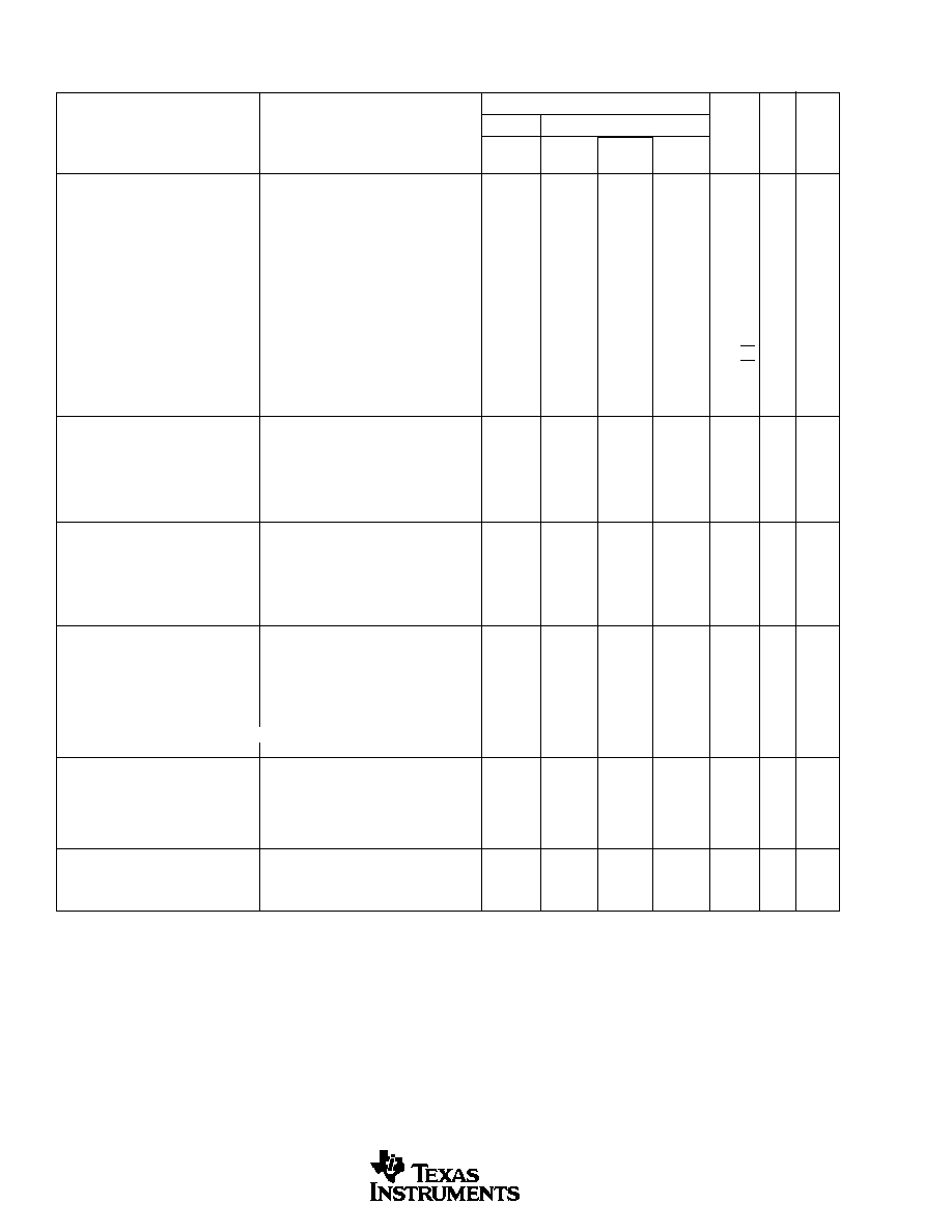
SPECIFICATIONS: V
S
= +5V
At T
A
= 25
∞
C, G = +2, R
F
= 750
, and R
L
= 150
to V
S
/2, unless otherwise noted.
AC PERFORMANCE (Figure 1)
Small-Signal Bandwidth
G = +2, V
O
0.5Vp-p
75
50
40
32
MHz
min
B
G = +5, V
O
0.5Vp-p
16
12
10
8.5
MHz
min
B
G = +10, V
O
0.5Vp-p
7.6
5.6
4.2
3.7
MHz
min
B
Gain Bandwidth Product
G
+10
68
51
40
36
MHz
min
B
Peaking at a Gain of +1
V
O
0.5Vp-p
5
--
--
--
dB
typ
C
Slew Rate
G = +2, 2V Step
100
64
52
47
V/
µ
s
min
B
Rise Time
0.5V Step
5.3
8.0
11
12.8
ns
max
B
Fall Time
0.5V Step
5.4
7.5
10
11.6
ns
max
B
Settling Time to 0.1%
G = +2, 1V Step
17
28
38
42
ns
max
B
Spurious Free Dynamic Range
V
O
= 2Vp-p, f = 5MHz
44
40
38
35
dB
min
B
V
O
= 2Vp-p, f = 1MHz, R
L
= 1k
84
68
66
62
dB
min
B
Input Voltage Noise
f > 1MHz
6.0
6.8
7.6
7.9
nV/
Hz
max
B
Input Current Noise
f > 1MHz
1.9
2.6
2.9
3.6
pA/
Hz
max
B
NTSC Differential Gain
0.5
--
--
--
%
typ
C
NTSC Differential Phase
1.2
--
--
--
degrees
typ
C
Channel-to-Channel Isolation
Input Referred, f = 5MHz
93
--
--
--
dB
typ
C
DC PERFORMANCE
Open-Loop Voltage Gain
62
56
50
46
dB
min
A
Input Offset Voltage
2.5
6
8
11
mV
max
A
Average Offset Voltage Drift
--
--
--
50
µ
V/
∞
C
max
B
Input Bias Current
V
CM
= 2.0V
11
25
31
48
µ
A
max
A
Input Offset Current
V
CM
= 2.0V
0.3
1.5
1.8
2.8
µ
A
max
A
Input Offset Current Drift
--
--
--
7
nA/
∞
C
max
B
INPUT
Least Positive Input Voltage
≠0.5
≠0.1
≠0.1
≠0.1
V
max
B
Most Positive Input Voltage
4.0
3.7
3.7
3.5
V
min
A
Common-Mode Rejection Ratio (CMRR)
Input Referred
74
70
68
60
dB
min
A
Input Impedance
Differential-Mode
10 || 2.1
--
--
--
k
|| pF
typ
C
Common-Mode
400 || 1.2
--
--
--
k
|| pF
typ
C
OUTPUT
Least Positive Output Voltage
R
L
= 1k
to 2.5V
0.03
0.07
0.10
0.13
V
max
A
R
L
= 150
to 2.5V
0.16
0.17
0.20
1.7
V
max
A
Most Positive Output Voltage
R
L
= 1k
to 2.5V
4.87
4.8
4.7
4.6
V
min
A
R
L
= 150
to 2.5V
4.60
4.4
4.4
3.1
V
min
A
Current Output, Sourcing
80
25
20
5
mA
min
A
Current Output, Sinking
90
31
19
8
mA
min
A
Short-Circuit Current (output shorted to either supply)
100
--
--
--
mA
typ
C
Closed-Loop Output Impedance
Figure 1, f
50kHz
0.6
--
--
--
typ
C
POWER SUPPLY
Minimum Operating Voltage
--
2.7
2.7
2.7
V
min
B
Maximum Operating Voltage
--
10.5
10.5
10.5
V
max
A
Maximum Quiescent Current
V
S
= +5V
6
6.6
6.9
7.1
mA/chan
max
A
Minimum Quiescent Current
V
S
= +5V
6
5.8
5.5
4.8
mA/chan
min
A
Power Supply Rejection Ratio (PSRR)
Input Referred
59
52
49
48
dB
min
A
THERMAL CHARACTERISTICS
Specification: U
≠40 to +85
--
--
--
∞
C
typ
C
Thermal Resistance
U
SO-8
125
--
--
--
∞
C/W
typ
C
NOTE: (1) Test Levels: (A) 100% tested at 25
∞
C. Over temperature limits by characterization and simulation. (B) Limits set by characterization and simulation.
(C) Typical value only for information.

OPA2631
3
SBOS067A
SPECIFICATIONS: V
S
= +3V
At T
A
= 25
∞
C, G = +2, R
F
= 750
, and R
L
= 150
to V
S
/2, unless otherwise noted.
OPA2631U
TYP
GUARANTEED
0
∞
C to
MIN/
TEST
PARAMETER
CONDITIONS
+25
∞
C
+25
∞
C
70
∞
C
UNITS
MAX LEVEL
(1)
AC PERFORMANCE (Figure 2)
Small-Signal Bandwidth
G = +2, V
O
0.5Vp-p
61
45
35
MHz
min
B
G = +5, V
O
0.5Vp-p
15
11
9
MHz
min
B
G = +10, V
O
0.5Vp-p
7.7
4.6
4.0
MHz
min
B
Gain Bandwidth Product
G
+10
63
47
34
MHz
min
B
Peaking at a Gain of +1
V
O
0.5Vp-p
5
--
--
dB
typ
C
Slew Rate
1V Step
95
52
46
V/
µ
s
min
B
Rise Time
0.5V Step
5.6
9
11.3
ns
max
B
Fall Time
0.5V Step
5.6
9
11.3
ns
max
B
Settling Time to 0.1%
1V Step
40
63
85
ns
max
B
Spurious Free Dynamic Range
V
O
= 1Vp-p, f = 5MHz
44
37
34
dB
min
B
V
O
= 1Vp-p, f = 1MHz, R
L
= 1k
84
67
65
dB
min
B
Input Voltage Noise
f > 1MHz
6.2
7.0
7.8
nV/
Hz
max
B
Input Current Noise
f > 1MHz
2.0
2.6
2.9
pA/
Hz
max
B
Channel-to-Channel Isolation
Input Reference, f = 5MHz
93
--
--
dB
typ
C
DC PERFORMANCE
Open-Loop Voltage Gain
60
54
50
dB
min
A
Input Offset Voltage
0.5
4.0
4.5
mV
max
A
Average Offset Voltage Drift
--
--
45
µ
V/
∞
C
max
B
Input Bias Current
V
CM
= 1.0V
12
25
30
µ
A
max
A
Input Offset Current
V
CM
= 1.0V
0.3
1
1.3
µ
A
max
A
Input Offset Current Drift
--
--
2
nA/
∞
C
max
B
INPUT
Least Positive Input Voltage
≠0.5
≠0.3
≠0.1
V
max
B
Most Positive Input Voltage
2
1.75
1.3
V
min
A
Common-Mode Rejection Ratio (CMRR)
Input Referred
72
66
65
dB
min
A
Input Impedance
Differential-Mode
10 || 2.1
--
--
k
|| pF
typ
C
Common-Mode
400 || 1.2
--
--
k
|| pF
typ
C
OUTPUT
Least Positive Output Voltage
R
L
= 1k
to 1.5V
0.03
0.05
0.05
V
max
A
R
L
= 150
to 1.5V
0.05
0.15
0.16
V
max
A
Most Positive Output Voltage
R
L
= 1k
to 1.5V
2.95
2.85
2.84
V
min
A
R
L
= 150
to 1.5V
2.85
2.66
2.60
V
min
A
Current Output, Sourcing
55
21
14
mA
min
A
Current Output, Sinking
55
18
11
mA
min
A
Short Circuit Current (output shorted to either supply)
80
--
--
mA
typ
C
Closed-Loop Output Impedance
Figure 2, f < 50kHz
0.6
--
--
typ
C
POWER SUPPLY
Minimum Operating Voltage
--
2.7
2.7
V
min
B
Maximum Operating Voltage
--
10.5
10.5
V
max
A
Maximum Quiescent Current
V
S
= +3V
5.3
5.9
6.4
mA/chan
max
A
Minimum Quiescent Current
V
S
= +3V
5.3
5.0
4.8
mA/chan
min
A
Power Supply Rejection Ratio (PSRR)
Input Referred
57
50
48
dB
min
A
THERMAL CHARACTERISTICS
Specification: U
≠40 to +85
∞
C
typ
C
Thermal Resistance
U
SO-8
125
∞
C/W
typ
C
NOTE: (1) Test Levels: (A) 100% tested at 25
∞
C. Over temperature limits by characterization and simulation. (B) Limits set by characterization and simulation.
(C) Typical value only for information.
OPA2631
4
SBOS067A
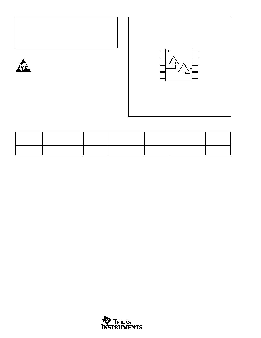
PIN CONFIGURATIONS
Top View
SO
1
2
3
4
8
7
6
5
+V
S
Out B
≠In B
+In B
Out A
≠In A
+In A
GND
OPA2631
ABSOLUTE MAXIMUM RATINGS
Power Supply ................................................................................ +11V
DC
Internal Power Dissipation .................................... See Thermal Analysis
Differential Input Voltage ..................................................................
±
1.2V
Input Voltage Range .................................................... ≠0.5 to +V
S
+0.3V
Storage Temperature Range ......................................... ≠40
∞
C to +125
∞
C
Lead Temperature (soldering, 10s) .............................................. +300
∞
C
Junction Temperature (T
J
) ........................................................... +175
∞
C
ELECTROSTATIC
DISCHARGE SENSITIVITY
Electrostatic discharge can cause damage ranging from perfor-
mance degradation to complete device failure. Burr-Brown Corpo-
ration recommends that all integrated circuits be handled and stored
using appropriate ESD protection methods.
ESD damage can range from subtle performance degradation to
complete device failure. Precision integrated circuits may be more
susceptible to damage because very small parametric changes
could cause the device not to meet published specifications.
PACKAGE
SPECIFIED
DRAWING
TEMPERATURE
PACKAGE
ORDERING
TRANSPORT
PRODUCT
PACKAGE
NUMBER
RANGE
MARKING
NUMBER
(1)
MEDIA
OPA2631U
SO-8 Surface-Mount
182
≠40
∞
C to +85
∞
C
OPA2631
OPA2631U
Rails
"
"
"
"
"
OPA2631U/2K5
Tape and Reel
NOTE: (1) Models with a slash (/) are available only in Tape and Reel in the quantities indicated (e.g., /2K5 indicates 2500 devices per reel). Ordering 2500 pieces
of "OPA2631U/2K5" will get a single 2500-piece Tape and Reel.
PACKAGE/ORDERING INFORMATION
OPA2631
5
SBOS067A
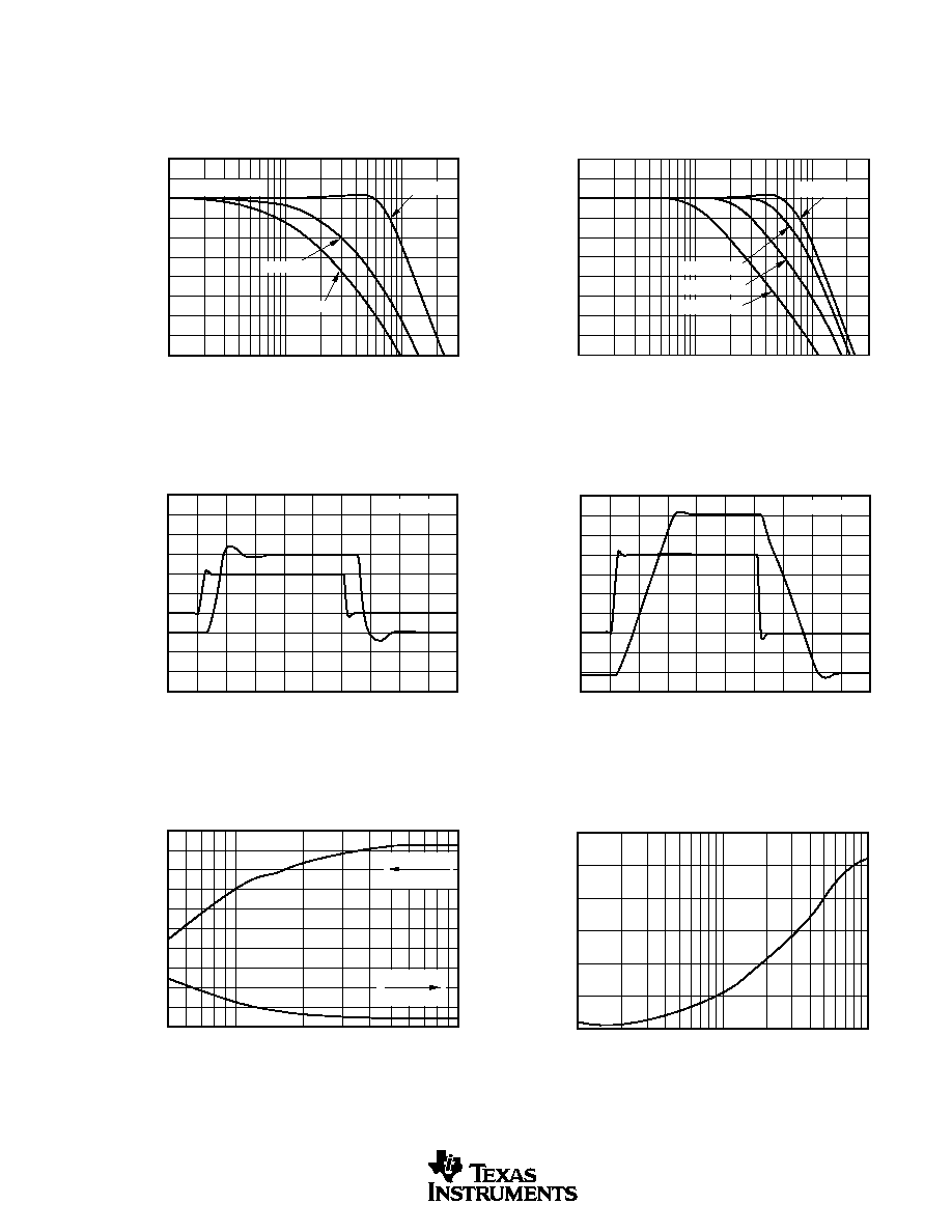
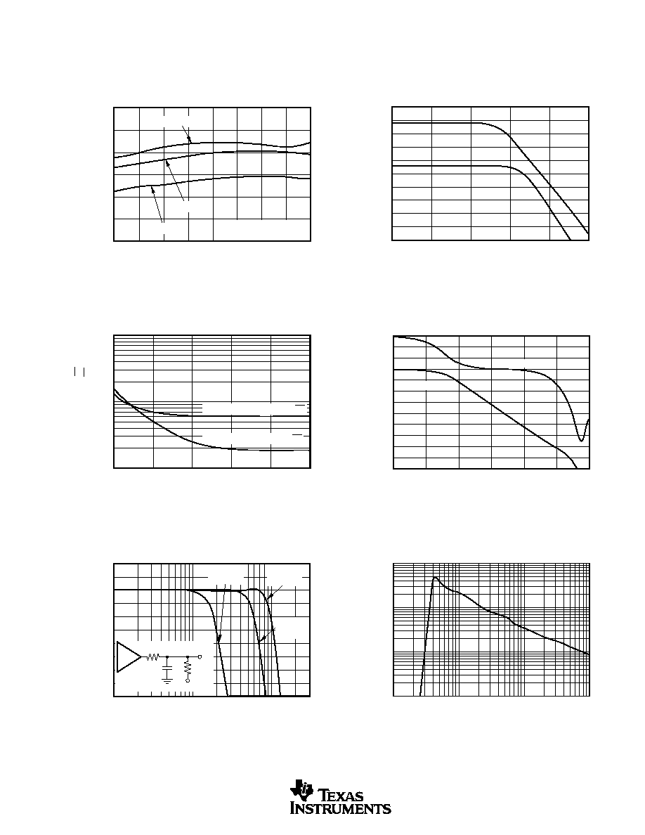
TYPICAL PERFORMANCE CURVES: V
S
= +5V
At T
A
= 25
∞
C, G = +2, R
F
= 750
, and R
L
= 150
to V
S
/2, unless otherwise noted (see Figure 2).
6
3
0
≠3
≠6
≠9
≠12
≠15
≠18
≠21
≠24
SMALL-SIGNAL FREQUENCY RESPONSE
Frequency (MHz)
Normalized Gain (dB)
1
10
100
300
V
O
= 200mVp-p
G = +10
G = +5
G = +2
12
9
6
3
0
≠3
≠6
≠9
≠12
≠15
≠18
LARGE-SIGNAL FREQUENCY RESPONSE
Frequency (MHz)
Gain (dB)
1
10
100
300
V
O
= 0.2Vp-p
V
O
= 4Vp-p
V
O
= 2Vp-p
V
O
= 1Vp-p
SMALL-SIGNAL PULSE RESPONSE
Time (10ns/div)
Input and Output Voltage (50mV/div)
V
O
= 200mVp-p
V
O
V
IN
5.0
4.9
4.8
4.7
4.6
4.5
4.4
4.3
4.2
4.1
4.0
OUTPUT SWING vs LOAD RESISTANCE
R
L
(
)
50
100
1000
Maximum Output Voltage (V)
1.0
0.9
0.8
0.7
0.6
0.5
0.4
0.3
0.2
0.1
0.0
Minimum Output Voltage (V)
Maximum V
O
Minimum V
O
Right Scale
Left Scale
LARGE-SIGNAL PULSE RESPONSE
Time (10ns/div)
Input and Output Voltage (500mV/div)
V
O
= 4Vp-p
V
O
V
IN
≠40
≠50
≠60
≠70
≠80
≠90
≠100
CHANNEL-TO-CHANNEL CROSSTALK
Frequency (MHz)
1
10
100
Input-Refered Isolation (dB)

OPA2631
6
SBOS067A
TYPICAL PERFORMANCE CURVES: V
S
= +5V
(Cont.)
At T
A
= 25
∞
C, G = +2, R
F
= 750
, and R
L
= 150
to V
S
/2, unless otherwise noted (see Figure 1).
≠30
≠40
≠50
≠60
≠70
≠80
HARMONIC DISTORTION vs OUTPUT VOLTAGE
Output Voltage (Vp-p)
0.1
1
f = 5MHz
4
Harmonic Distortion (dBc)
3rd Harmonic
2nd Harmonic
≠30
≠40
≠50
≠60
≠70
≠80
HARMONIC DISTORTION vs INVERTING GAIN
Gain Magnitude (V/V)
1
10
Harmonic Distortion (dBc)
V
O
= 2Vp-p
f = 5MHz
3rd Harmonic
2nd Harmonic
≠30
≠40
≠50
≠60
≠70
≠80
HARMONIC DISTORTION vs FREQUENCY
Frequency (MHz)
1
0.1
10
Harmonic Distortion (dBc)
V
O
= 2Vp-p
3rd Harmonic
2nd Harmonic
≠30
≠40
≠50
≠60
≠70
≠80
HARMONIC DISTORTION vs LOAD RESISTANCE
R
L
(
)
100
1000
Harmonic Distortion (dBc)
V
O
= 2Vp-p
f
O
= 5MHz
3rd Harmonic
2nd Harmonic
≠30
≠40
≠50
≠60
≠70
≠80
HARMONIC DISTORTION vs SUPPLY VOLTAGE
Single-Supply Voltage (V)
3
8
9
7
6
5
4
10
Harmonic Distortion (dBc)
V
O
= 2Vp-p
f
O
= 5MHz
3rd Harmonic
2nd Harmonic
≠30
≠40
≠50
≠60
≠70
≠80
HARMONIC DISTORTION vs NON-INVERTING GAIN
Gain Magnitude (V/V)
1
10
Harmonic Distortion (dBc)
V
O
= 2Vp-p
f = 5MHz
3rd Harmonic
2nd Harmonic
OPA2631
7
SBOS067A
TYPICAL XPERFORMANCE CURVES: V
S
=+5V
(Cont.)
At T
A
= 25
∞
C, G = +2, R
F
= 750
, and R
L
= 150
to V
S
/2, unless otherwise noted (see Figure 1).
100
10
1
INPUT NOISE DENSITY vs FREQUENCY
Frequency (Hz)
100
1K
10K
100K
1M
10M
Voltage Noise (nV/
Hz)
Current Noise (pA/
Hz)
Voltage Noise, e
ni
= 6.0nV/
Hz
Current Noise, i
ni
= 1.9pA/
Hz
2
1
0
≠1
≠2
≠3
≠4
≠5
≠6
≠7
≠8
FREQUENCY RESPONSE vs CAPACITIVE LOAD
Frequency (MHz)
1
10
100
300
Normalized Gain (dB)
R
S
1/2
OPA2631
V
O
1k
C
L
+V
S
/2
C
L
= 100pF
R
S
= 35.7
C
L
=1000pF
R
S
= 10
C
L
= 10pF
R
S
= 249
≠30
≠40
≠50
≠60
≠70
≠80
≠90
TWO-TONE, 3rd-ORDER
INTERMODULATION SPURIOUS
Single-Tone Load Power (dBm)
≠16
≠14
≠12
≠10
≠8
≠6
≠4
≠2
0
3rd-Order Spurious Level (dBc)
Load Power at
Matched 50
Load
f
O
= 1MHz
f
O
= 5MHz
f
O
= 10MHz
80
75
70
65
60
55
50
45
40
35
30
CMRR AND PSRR vs FREQUENCY
Frequency (Hz)
100
1K
10K
100K
1M
10M
Rejection Ratio, Input Referred (dB)
CMRR
PSRR
100
90
80
70
60
50
40
30
20
10
0
≠10
≠20
OPEN-LOOP GAIN AND PHASE
Frequency (Hz)
1K
10K
100K
1M
10M
100M
1G
Open-Loop Gain (dB)
0
≠30
≠60
≠90
≠120
≠150
≠180
≠210
≠240
≠270
≠300
≠330
≠360
Open-Loop Phase (
∞
)
Open-Loop Phase
Open-Loop Gain
1000
100
10
1
RECOMMENDED R
S
vs CAPACITIVE LOAD
Capacitive Load (pF)
1
10
100
1000
R
S
(
)
OPA2631
8
SBOS067A
TYPICAL PERFORMANCE CURVES: V
S
= +5V
(Cont.)
At T
A
= 25
∞
C, G = +2, R
F
= 750
, and R
L
= 150
to V
S
/2, unless otherwise noted (see Figure 1).
100
10
1
0.1
CLOSED-LOOP OUTPUT IMPEDANCE
vs FREQUENCY
Frequency (Hz)
1k
10k
100k
1M
10M
100M
Output Impedance (
)
G = +1
R
F
= 25
5.0
4.5
4.0
3.5
3.0
2.5
2.0
1.5
1.0
0.5
0.0
INPUT DC ERRORS vs TEMPERATURE
Temperature (
∞
C)
≠40
≠20
0
20
40
60
80
100
Input Offset Voltage (mV)
20
18
16
14
12
10
8
6
4
2
0
Input Bias Current (
µ
A)
10x Input Offset Current (
µ
A)
Input Offset Voltage
Input Bias Current
10X Input Offset Current
12
10
8
6
4
2
0
POWER SUPPLY AND OUTPUT CURRENT
vs TEMPERATURE
Temperature (
∞
C)
≠40
≠20
0
20
40
60
80
100
Quiescent Supply Current (mA)
120
100
80
60
40
20
0
Output Current (mA)
Sourcing Output Current
Sinking Output Current
Quiescent Supply Current
OPA2631
9
SBOS067A
6
3
0
≠3
≠6
≠9
≠12
≠15
≠18
≠21
≠24
SMALL-SIGNAL FREQUENCY RESPONSE
Frequency (MHz)
Normalized Gain (dB)
1
10
100
300
V
O
= 200mVp-p
G = +10
G = +2
G = +5
12
9
6
3
0
≠3
≠6
≠9
≠12
≠15
≠18
LARGE-SIGNAL FREQUENCY RESPONSE
Frequency (MHz)
Gain (dB)
1
10
100
300
V
O
= 2Vp-p
V
O
= 200mVp-p
V
O
= 1Vp-p
TYPICAL PERFORMANCE CURVES: V
S
= +3V
At T
A
= 25
∞
C, G = +2, R
F
= 750
, and R
L
= 150
to V
S
/2, unless otherwise noted (see Figure 1).
≠30
≠40
≠50
≠60
≠70
≠80
≠90
TWO-TONE, 3rd-ORDER
INTERMODULATION SPURIOUS
Single-Tone Load Power (dBm)
≠16
≠14
≠12
≠10
≠8
≠6
≠4
3rd-Order Spurious Level (dBc)
Load Power at
Matched 50
Load
f
O
= 10MHz
f
O
= 1MHz
f
O
= 5MHz
6
3
0
≠3
≠6
≠9
≠12
≠15
≠18
≠21
≠24
FREQUENCY RESPONSE vs CAPACITIVE LOAD
Frequency (MHz)
1
10
100
300
Normalized Gain (dB)
V
O
= 0.2Vp-p
R
S
1/2
OPA2631
V
O
1k
C
L
+V
S
/2
C
L
= 100pF
R
S
= 35.7
C
L
= 1000pF
R
S
= 10
C
L
= 10pF
R
S
= 249
3.0
2.9
2.8
2.7
2.6
2.5
2.4
2.3
2.2
2.1
2.0
OUTPUT SWING vs LOAD RESISTANCE
R
L
(
)
50
100
1000
Maximum Output Voltage (V)
1.0
0.9
0.8
0.7
0.6
0.5
0.4
0.3
0.2
0.1
0.0
Minimum Output Voltage (V)
Maximum V
O
Minimum V
O
Right Scale
Left Scale
1000
100
10
1
RECOMMENDED R
S
vs CAPACITIVE LOAD
Capacitive Load (pF)
1
10
100
1000
R
S
(
)
OPA2631
10
SBOS067A
TYPICAL PERFORMANCE CURVES: V
S
= +3V
(Cont.)
At T
A
= 25
∞
C, G = +2, R
F
= 750
, and R
L
= 150
to V
S
/2, unless otherwise noted (see Figure 2).
120
100
80
60
40
20
0
SLEW RATE AND GAIN BANDWIDTH PRODUCT
vs SUPPLY VOLTAGE
Supply Voltage (V)
3
4
5
6
7
8
9
10
Slew Rate (V/
µ
s)
120
100
80
60
40
20
0
Gain Bandwidth Product (MHz)
Slew Rate
Gain Bandwidth Product
10
9
8
7
6
5
4
3
2
1
0
SUPPLY AND OUTPUT CURRENTS
vs SUPPLY VOLTAGE
Supply Voltage (V)
3
4
5
6
7
8
9
10
Quiescent Supply Current (mA/chan)
200
180
160
140
120
100
80
60
40
20
0
Output Current (mA)
Quiescent Supply Current
Output Current, Sourcing
Output Current, Sinking
OPA2631
11
SBOS067A
APPLICATIONS INFORMATION
WIDEBAND VOLTAGE-FEEDBACK OPERATION
The OPA2631 is a unity-gain stable, very high-speed, volt-
age-feedback op amp designed for single-supply operation
(+3V to +10V). The input stage supports input voltages
below ground, and to within 1.0V of the positive supply. The
complementary common-emitter output stage provides an
output swing to within 30mV of ground and 130mV of the
positive supply. It is compensated to provide stable opera-
tion with a wide range of resistive loads.
Figure 1 shows the AC-coupled, gain of +2 configuration
used for the +5V Specifications and Typical Performance
Curves. For test purposes, the input impedance is set to 50
with a resistor to ground. Voltage swings reported in the
Specifications are taken directly at the input and output pins.
For the circuit of Figure 1, the total effective load on the
output at high frequencies is 150
|| 1500
. The 1.50k
resistors at the non-inverting input provide the common-
mode bias voltage. Their parallel combination equals the DC
resistance at the inverting input, minimizing the output DC
offset.
1/2
OPA2631
+V
S
= 5V
V
OUT
53.6
V
IN
R
F
750
R
G
750
1.50k
1.50k
R
L
150
+V
S
2
6.8
µ
F
+
0.1
µ
F
0.1
µ
F
0.1
µ
F
FIGURE 1. AC-Coupled Signal--Resistive Load to Supply
Midpoint.
FIGURE 2. DC-Coupled Signal--Resistive Load to Supply
Midpoint.
1/2
OPA2631
+V
S
= 3V
V
OUT
57.6
V
IN
374
2.26k
R
L
150
+V
S
2
6.8
µ
F
+
0.1
µ
F
R
F
750
R
G
562
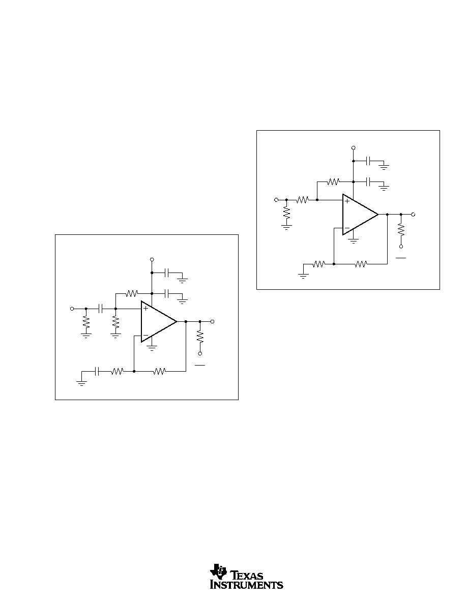
Figure 2 shows the DC-coupled, gain of +2 configuration
used for the +3V Specifications and Typical Performance
Curves. For test purposes, the input impedance is set to 50
with a resistor to ground. Though not strictly a "rail-to-rail"
design, this part comes very close, while maintaining excel-
lent performance. It will deliver
2.9Vp-p on a single +3V
supply with 61MHz bandwidth. The 374
and 2.26k
resistors at the input level-shift V
IN
so that V
OUT
is within
the allowed output voltage range when V
IN
= 0. See the
typical performance curves for information on driving ca-
pacitive loads.
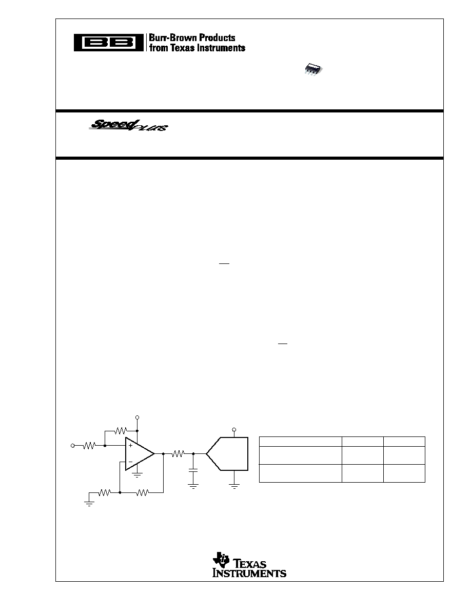
SINGLE-SUPPLY ADC CONVERTER INTERFACE
The front page shows a DC-coupled, single-supply, dual
ADC (Analog-to-Digital Converter) driver circuit. Many
systems are now requiring +3V supply capability of both the
ADC and its driver. The OPA2631 provides excellent per-
formance in this demanding application. Its large input and
output voltage ranges, and low distortion support converters
such as the ADS901 shown in this figure. The input level-
shifting circuitry was designed so that V
IN
can be between
0V and 0.5V, while delivering an output voltage of 1V to 2V
for the ADS901.
OPA2631
12
SBOS067A
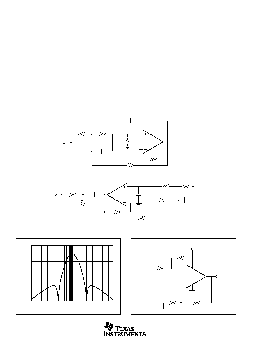
BANDPASS FILTER
Figure 3 shows a single OPA2631 implementing a 6th-order
bandpass filter. This filter cascades two 2nd-order Sallen-
Key sections with transmission zeros, and a double real pole
section. It has ≠3dB frequencies of 630kHz and 1.5MHz,
and ≠40dB frequencies of 230kHz and 4.2MHz. This filter
was designed to work well on +5V or
±
5V supplies, while
driving an A/D converter at 6MSPS to 10MSPS (e.g., the
ADS804).
The filter transfer function is based on a 4th-order elliptic
bandpass filter, with real highpass and lowpass poles added
at the output to give a 6th-order response. The components
were chosen to give this transfer function. The 20
resistor
isolates the first OPA2631 output from capacitive loading,
but affects the response at very high frequencies only. Figure
4 shows the nominal response simulated by SPICE
Æ
.
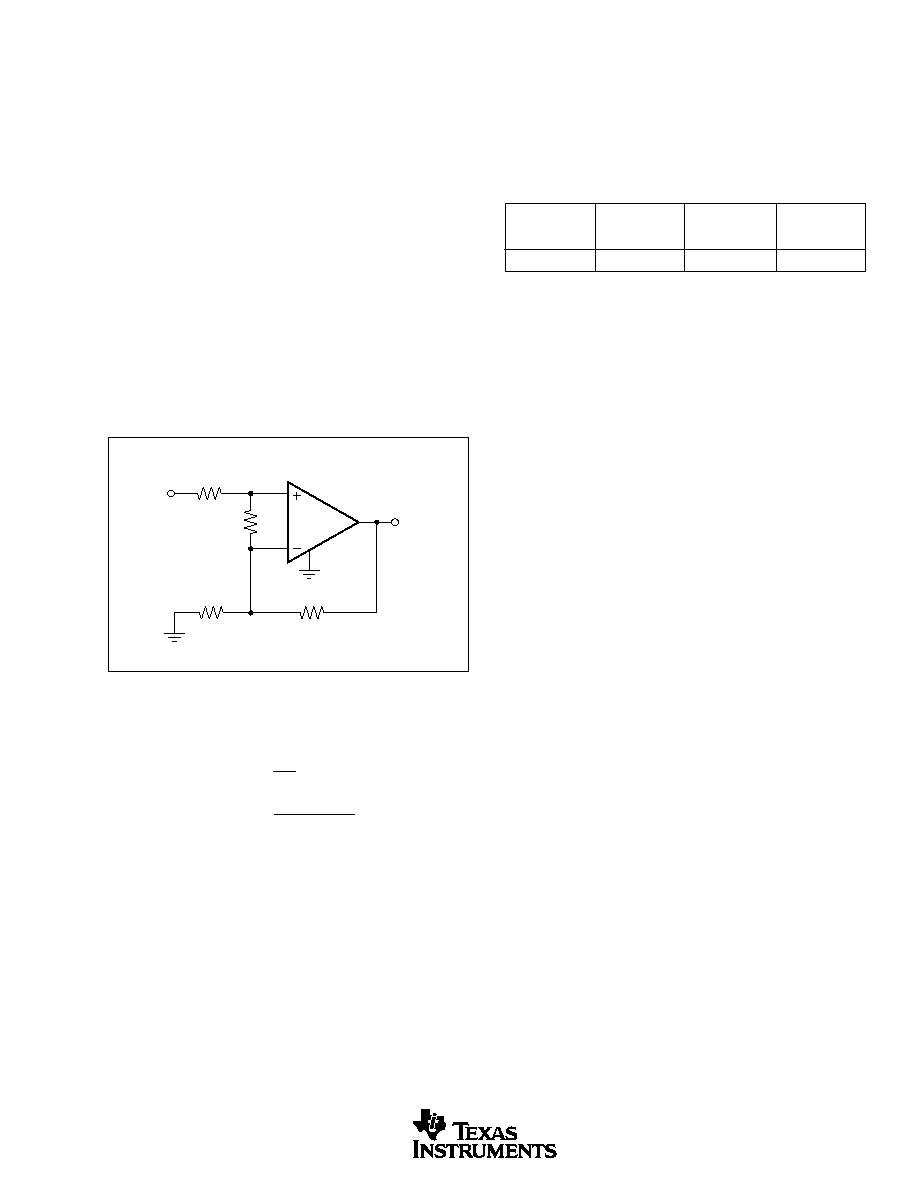
DC LEVEL SHIFTING
Figure 5 shows a DC-coupled non-inverting amplifier that
level-shifts the input up to accommodate the desired output
voltage range. Given the desired signal gain (G) and the
amount V
OUT
needs to be shifted up (
V
OUT
), when V
IN
is
at the center of its range, the following equations give the
resistor values that produce the desired performance. Start
by setting R
4
between 200
and 1.5k
.
NG = G +
V
OUT
/V
S
R
1
= R
4
/G
R
2
= R
4
/(NG ≠ G)
R
3
= R
4
/(NG ≠1)
where:
NG = 1 + R
4
/R
3
(Noise Gain)
V
OUT
= (G)V
IN
+ (NG ≠ G)V
S
10
0
≠10
≠20
≠30
≠40
≠50
≠60
Frequency (Hz)
Gain (dB)
10K
1M
10M
100K
100M
1/2
OPA2631
+V
S
V
OUT
V
IN
R
3
R
2
R
1
R
4
FIGURE 3. Bandpass Filter.
FIGURE 4. Nominal Filter Response.
FIGURE 5. DC Level Shifting Circuit.
1/2
OPA2631
86.6
V
IN
60.4
7.32k
200
2.2nF
1% Resistors
5% Capacitors
27pF
3.9nF
3.9nF
1.2nF
130
59
1/2
OPA2631
46.4
20
133
73.2
V
OUT
1.2nF
200
1.8nF
1.2nF
681
330pF
OPA2631
13
SBOS067A
Make sure that V
IN
and V
OUT
stay within the specified input
and output voltage ranges.
The front page circuit is a good example of this type of
application. It was designed to take V
IN
between 0V and 0.5V,
and produce V
OUT
between 1V and 2V, when using a +3V
supply. This means G = 2.00, and
V
OUT
= 1.50V ≠ G ∑ 0.25V
= 1.00V. Plugging into the above equations (with R
4
= 750
)
gives: NG = 2.33, R
1
= 375
, R
2
= 2.25k
, and R
3
= 563
.
The resistors were adjusted to the nearest standard values.
NON-INVERTING AMPLIFIER WITH
REDUCED PEAKING
Figure 6 shows a non-inverting amplifier that reduces peak-
ing at low gains. The resistor R
C
compensates the OPA2631
to have higher Noise Gain (NG), which reduces the AC
response peaking (typically 5dB at G = +1 without R
C
)
without changing the DC gain. V
IN
needs to be a low
impedance source, such as an op amp. The resistor values
are low to reduce noise. Using both R
T
and R
F
helps
minimize the impact of parasitic impedances.
DESIGN-IN TOOLS
DEMONSTRATION BOARDS
A single PC board is available to assist in the initial evalu-
ation of circuit performance using the OPA2631U. It is
available free as an unpopulated PC board delivered with
descriptive documentation. The summary information for
this board is shown in Table I.
FIGURE 6. Compensated Non-Inverting Amplifier.
BOARD
LITERATURE
PART
REQUEST
PRODUCT
PACKAGE
NUMBER
NUMBER
OPA2631U
SO-8
DEM-OPA268xU
MKT-352
TABLE I. Demo Board Summary Information.
The Noise Gain can be calculated as follows:
G
R
R
G
R
R
G
R
NG
G G
F
G
T
F
C
1
2
1
1
2
1
1
= +
= +
+
=
/
A unity gain buffer can be designed by selecting
R
T
= R
F
= 20.0
and R
C
= 40.2
(do not use R
G
). This gives
a Noise Gain of 2, so its response will be similar to the
typical performance curves with G = +2 which typically
gives a flat frequency response, but with less bandwidth.
1/2
OPA2631
V
OUT
V
IN
R
G
R
T
R
F
R
C
Contact the Texas Instruments Technical Applications Sup-
port Line at 1-972-644-5580 to request this board.
OPERATING SUGGESTIONS
OPTIMIZING RESISTOR VALUES
Since the OPA2631 is a voltage-feedback op amp, a wide
range of resistor values may be used for the feedback and
gain setting resistors. The primary limits on these values are
set by dynamic range (noise and distortion) and parasitic
capacitance considerations. For a non-inverting unity gain
follower application, the feedback connection should be
made with a 20
resistor, not a direct short (see Figure 6).
This will isolate the inverting input capacitance from the
output pin and improve the frequency response flatness.
Usually, for G > 1 application, the feedback resistor value
should be between 200
and 1.5k
. Below 200
, the
feedback network will present additional output loading
which can degrade the harmonic-distortion performance.
Above 1.5k
, the typical parasitic capacitance (approxi-
mately 0.2pF) across the feedback resistor may cause unin-
tentional band-limiting in the amplifier response.
A good rule of thumb is to target the parallel combination of
R
F
and R
G
(Figure 1) to be less than approximately 400
.
The combined impedance (R
F
|| R
G
) interacts with the invert-
ing input capacitance, placing an additional pole in the
feedback network and thus, a zero in the forward response.
Assuming a 3pF total parasitic on the inverting node, hold-
ing R
F
|| R
G
< 400
will keep this pole above 130MHz. By
itself, this constraint implies that the feedback resistor R
F
can increase to several k
at high gains. This is acceptable
as long as the pole formed by R
F
, and any parasitic capaci-
tance appearing in parallel, is kept out of the frequency
range of interest.
OPA2631
14
SBOS067A
BANDWIDTH VERSUS GAIN: NON-INVERTING OPERATION
Voltage-feedback op amps exhibit decreasing closed-loop
bandwidth as the signal gain is increased. In theory, this
relationship is described by the Gain Bandwidth Product
(GBP) shown in the Specifications table. Ideally, dividing
GBP by the non-inverting signal gain (also called the Noise
Gain, or NG) will predict the closed-loop bandwidth. In
practice, this only holds true when the phase margin ap-
proaches 90
∞
, as it does in high-gain configurations. At low
gains (increased feedback factors), most amplifiers will
exhibit a more complex response with lower phase margin.
The OPA2631 is compensated to give a slightly peaked
response in a non-inverting gain of 2 (Figure 1). This results
in a typical gain of +2 bandwidth of 75MHz, far exceeding
that predicted by dividing the 68MHz GBP by 2. Increasing
the gain will cause the phase margin to approach 90
∞
and the
bandwidth to more closely approach the predicted value of
(GBP/NG). At a gain of +10, the 7.6MHz bandwidth shown
in the Specifications table is close to that predicted using the
simple formula and the typical GBP.
The OPA2631 exhibits minimal bandwidth reduction going
to +3V single-supply operation as compared with +5V
supply. This is because the internal bias control circuitry
retains nearly constant quiescent current as the total supply
voltage between the supply pins is changed.
INVERTING AMPLIFIER OPERATION
Since the OPA2631 is a general-purpose, wideband voltage-
feedback op amp, all of the familiar op amp application
circuits are available to the designer. Figure 7 shows a typical
inverting configuration where the I/O impedances and signal
gain from Figure 1 are retained in an inverting circuit configu-
ration. Inverting operation is one of the more common
requirements and offers several performance benefits. The
inverting configuration shows improved slew rate and distor-
tion. It also biases the input at V
S
/2 for the best headroom. The
output voltage can be independently moved with bias adjust-
ment resistors connected to the inverting input.
In the inverting configuration, three key design consider-
ation must be noted. The first is that the gain resistor (R
G
)
becomes part of the signal channel input impedance. If input
impedance matching is desired (which is beneficial when-
ever the signal is coupled through a cable, twisted pair, long
PC board trace, or other transmission line conductor), R
G
may be set equal to the required termination value, and R
F
adjusted to give the desired gain. This is the simplest
approach and results in optimum bandwidth and noise per-
formance. However, at low inverting gains, the resultant
feedback resistor value can present a significant load to the
amplifier output. For an inverting gain of 2, setting R
G
to
50
for input matching eliminates the need for R
M
but
requires a 100
feedback resistor. This has the interesting
advantage of the noise gain becoming equal to 2 for a 50
source impedance--the same as the non-inverting circuits
considered above. However, the amplifier output will now
see the 100
feedback resistor in parallel with the external
load. In general, the feedback resistor should be limited to
the 200
to 1.5k
range. In this case, it is preferable to
increase both the R
F
and R
G
values, as shown in Figure 7,
and then achieve the input matching impedance with a third
resistor (R
M
) to ground. The total input impedance becomes
the parallel combination of R
G
and R
M
.
The second major consideration, touched on in the previous
paragraph, is that the signal source impedance becomes
part of the noise gain equation and hence influences the
bandwidth. For the example in Figure 7, the R
M
value
combines in parallel with the external 50
source imped-
ance, yielding an effective driving impedance of
50
|| 576
= 26.8
. This impedance is added in series
with R
G
for calculating the noise gain. The resultant is 2.87
for Figure 7, as opposed to only 2 if R
M
could be eliminated
as discussed above. The bandwidth will therefore be lower
for the gain of ≠2 circuit of Figure 7 (NG = +2.87) than for
the gain of +2 circuit of Figure 1.
The third important consideration in inverting amplifier
design is setting the bias current cancellation resistors on
the non-inverting input (a parallel combination of
R
T
= 750
). If this resistor is set equal to the total DC
resistance looking out of the inverting node, the output DC
error, due to the input bias currents, will be reduced to
(input offset current) ∑ R
F
. The inverting input's bias
current flows through R
F
because of the 0.1
µ
F capacitor.
Thus, we need R
T
= 750
= 1.50k
|| 1.50k
.
To reduce
the additional high-frequency noise introduced by this R
T
resistor, and power-supply feedthrough, it is bypassed
with a capacitor. If we had R
T
< 400
, its noise contribu-
tion would be minimal. As a minimum, the OPA2631
requires an R
T
value of 50
to damp out parasitic-induced
peaking--a direct short to ground on the non-inverting
input runs the risk of a very high-frequency instability in
the input stage.
FIGURE 7. Gain of ≠2 Example Circuit.
0.1
µ
F
1/2
OPA2631
50
R
F
750
R
G
374
2R
T
1.50k
R
M
57.6
Source
+5V
2R
T
1.50k
R
O
50
0.1
µ
F
6.8
µ
F
+
0.1
µ
F
50
Load
OPA2631
15
SBOS067A
(1)
E
O
=
E
NI
2
+
I
BN
R
S
(
)
2
+ 4
kTR
S
(
)
NG
2
+
I
BI
R
F
(
)
2
+ 4
kTR
F
NG
Dividing this expression by the noise gain (NG = (1 + R
F
/R
G
))
will give the equivalent input-referred spot noise voltage at
the non-inverting input, as shown in Equation 2.
(2)
E
N
=
E
NI
2
+
I
BN
R
S
(
)
2
+ 4
kTR
S
+
I
BI
R
F
NG
2
+ 4
kTR
F
NG
OUTPUT CURRENT AND VOLTAGE
The OPA2631 provides outstanding output voltage capabil-
ity. Under no-load conditions at +25
∞
C, the output voltage
typically swings closer than 130mV to either supply rail; the
guaranteed over temperature swing is within 400mV of
either rail (V
S
= +5V).
The minimum specified output voltage and current specifi-
cations over temperature are set by worst-case simulations at
the cold temperature extreme. Only at cold start-up will the
output current and voltage decrease to the numbers shown in
the guaranteed tables. As the output transistors deliver power,
their junction temperatures will increase, decreasing their
V
BE
's (increasing the available output voltage swing) and
increasing their current gains (increasing the available out-
put current). In steady-state operation, the available output
voltage and current will always be greater than that shown
in the over-temperature specifications, since the output stage
junction temperatures will be higher than the minimum
specified operating ambient.
To maintain maximum output stage linearity, no output
short-circuit protection is provided. This will not normally
be a problem, since most applications include a series
matching resistor at the output that will limit the internal
power dissipation if the output side of this resistor is shorted
to ground.
DRIVING CAPACITIVE LOADS
One of the most demanding and yet very common load
conditions for an op amp is capacitive loading. Often, the
capacitive load is the input of an ADC--including additional
external capacitance which may be recommended to im-
prove ADC linearity. A high-speed, high open-loop gain
amplifier like the OPA2631 can be very susceptible to
decreased stability and closed-loop response peaking when
a capacitive load is placed directly on the output pin. When
the primary considerations are frequency response flatness,
pulse response fidelity, and/or distortion, the simplest and
most effective solution is to isolate the capacitive load from
the feedback loop by inserting a series isolation resistor
between the amplifier output and the capacitive load.
The Typical Performance Curves show the recommended
R
S
versus capacitive load and the resulting frequency re-
sponse at the load. Parasitic capacitive loads greater than
2pF can begin to degrade the performance of the OPA2631.
Long PC board traces, unmatched cables, and connections to
multiple devices can easily exceed this value. Always con-
sider this effect carefully, and add the recommended series
resistor as close as possible to the output pin (see Board
Layout Guidelines section).
The criterion for setting this R
S
resistor is a maximum
bandwidth, flat frequency response at the load. For a gain of
+2, the frequency response at the output pin is already
slightly peaked without the capacitive load, requiring rela-
tively high values of R
S
to flatten the response at the load.
Increasing the noise gain will also reduce the peaking (see
Figure 6).
DISTORTION PERFORMANCE
The OPA2631 provides good distortion performance into a
150
load. Relative to alternative solutions, it provides
exceptional performance into lighter loads and/or operating
on a single +3V supply. Generally, the 3rd harmonic will
dominate the distortion. Focusing then on the 3rd harmonic,
increasing the load impedance improves distortion directly.
Remember that the total load includes the feedback network;
in the non-inverting configuration (Figure 1) this is sum of
R
F
+ R
G
, while in the inverting configuration, only R
F
needs
to be included in parallel with the actual load.
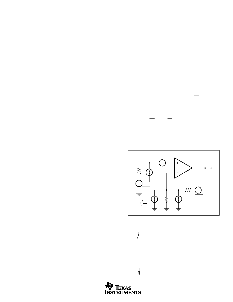
NOISE PERFORMANCE
High slew rate, unity gain stable, voltage-feedback op amps
usually achieve their slew rate at the expense of a higher
input noise voltage. The 6.0nV/
Hz input voltage noise for
the OPA2631 is, however, much lower than comparable
amplifiers. The input-referred voltage noise, and the two
input-referred current noise terms (1.9pA/
Hz), combine to
give low output noise under a wide variety of operating
conditions. Figure 8 shows the op amp noise analysis model
with all the noise terms included. In this model, all noise
terms are taken to be noise voltage or current density terms
in either nV/
Hz or pA/
Hz.
The total output spot noise voltage can be computed as the
square root of the sum of all squared output noise voltage
contributors. Equation 1 shows the general form for the
output noise voltage using the terms shown in Figure 8.
FIGURE 8. Noise Analysis Model.
4kT
R
G
R
G
R
F
R
S
1/2
OPA2631
I
BI
E
O
I
BN
4kT = 1.6 ∑ 10
≠20
J
at 290
∞
K
E
RS
E
NI
4kTR
S
4kTR
F

OPA2631
16
SBOS067A
Evaluating these two equations for the circuit and compo-
nent values shown in Figure 1 will give a total output spot
noise voltage of 13.1nV/
Hz and a total equivalent input
spot noise voltage of 6.6nV/
Hz. This is including the noise
added by the resistors. This total input-referred spot noise
voltage is not much higher than the 6.0nV/
Hz specification
for the op amp voltage noise alone. This will be the case as
long as the impedances appearing at each op amp input are
limited to the previously recommend maximum value of
400
, and the input attenuation is low.
DC ACCURACY AND OFFSET CONTROL
The balanced input stage of a wideband voltage-feedback op
amp allows good output DC accuracy in a wide variety of
applications. The power-supply current trim for the OPA2631
gives even tighter control than comparable products. Al-
though the high-speed input stage does require relatively
high input bias current (typically 11
µ
A out of each input
terminal), the close matching between them may be used to
reduce the output DC error caused by this current. This is
done by matching the DC source resistances appearing at the
two inputs. Evaluating the configuration of Figure 1 (which
has matched DC input resistances), using worst-case +25
∞
C
input offset voltage and current specifications, gives a worst-
case output offset voltage equal to: (NG = non-inverting
signal gain at DC)
±
(NG ∑ V
OS(MAX)
)
±
(R
F
∑ I
OS(MAX)
)
=
±
(1 ∑ 6.0mV)
±
(750
∑ 1.5
µ
A)
=
±
7.1mV [Output Offset Range for Figure 1]
A fine scale output offset null, or DC operating point
adjustment, is often required. Numerous techniques are
available for introducing DC offset control into an op amp
circuit. Most of these techniques are based on adding a DC
current through the feedback resistor. In selecting an offset
trim method, one key consideration is the impact on the
desired signal path frequency response. If the signal path is
intended to be non-inverting, the offset control is best
applied as an inverting summing signal to avoid interaction
with the signal source. If the signal path is intended to be
inverting, applying the offset control to the non-inverting
input may be considered. Bring the DC offsetting current
into the inverting input node through resistor values that are
much larger than the signal path resistors. This will insure
that the adjustment circuit has minimal effect on the loop
gain and hence the frequency response.
THERMAL ANALYSIS
Maximum desired junction temperature will set the maxi-
mum allowed internal power dissipation as described below.
In no case should the maximum junction temperature be
allowed to exceed 175
∞
C.
Operating junction temperature (T
J
) is given by T
A
+ P
D
∑
JA
.
The total internal power dissipation (P
D
) is the sum of
quiescent power (P
DQ
) and additional power dissipated in the
output stage (P
DL
) to deliver load power. Quiescent power is
simply the specified no-load supply current times the total
supply voltage across the part. P
DL
will depend on the
required output signal and load but would, for resistive load
connected to mid-supply (V
S
/2), be at a maximum when the
output is fixed at a voltage equal to V
S
/4 or 3V
S
/4. Under this
condition, P
DL
= V
S
2
/(16 ∑ R
L
), where R
L
includes feedback
network loading.
Note that it is the power in the output stage, and not into the
load, that determines internal power dissipation.
As a worst-case example, compute the maximum T
J
using
the circuit of Figure 1 operating at the maximum specified
ambient temperature of +85
∞
C and driving a 150
load at
mid-supply, for both channels:
P
D
= 2 (10V ∑ 7.1mA + 5
2
/(16 ∑ (150
|| 1500
))) = 161mW
Maximum T
J
= +85
∞
C + (0.16W ∑ 150
∞
C/W) = 109
∞
C.
Although this is still well below the specified maximum
junction temperature, system reliability considerations may
require lower guaranteed junction temperatures. The highest
possible internal dissipation will occur if the load requires
current to be forced into the output at high output voltages
or sourced from the output at low output voltages. This puts
a high current through a large internal voltage drop in the
output transistors.
BOARD LAYOUT GUIDELINES
Achieving optimum performance with a high frequency
amplifier like the OPA2631 requires careful attention to
board layout parasitics and external component types. Rec-
ommendations that will optimize performance include:
a) Minimize parasitic capacitance to any AC ground for
all of the signal I/O pins. Parasitic capacitance on the output
and inverting input pins can cause instability: on the non-
inverting input, it can react with the source impedance to
cause unintentional bandlimiting. To reduce unwanted ca-
pacitance, a window around the signal I/O pins should be
opened in all of the ground and power planes around those
pins. Otherwise, ground and power planes should be unbro-
ken elsewhere on the board.
b) Minimize the distance (<0.25") from the power-supply
pins to high frequency 0.1
µ
F decoupling capacitors. At the
device pins, the ground and power plane layout should not
be in close proximity to the signal I/O pins. Avoid narrow
power and ground traces to minimize inductance between
the pins and the decoupling capacitors. Each power-supply
connection should always be decoupled with one of these
capacitors. An optional supply decoupling capacitor (0.1
µ
F)
across the two power supplies (for bipolar operation) will
improve 2nd-harmonic distortion performance. Larger (2.2
µ
F
to 6.8
µ
F) decoupling capacitors, effective at lower fre-
quency, should also be used on the main supply pins. These
may be placed somewhat farther from the device and may be
shared among several devices in the same area of the PC
board.
OPA2631
17
SBOS067A
c) Careful selection and placement of external compo-
nents will preserve high frequency performance. Resis-
tors should be a very low reactance type. Surface-mount
resistors work best and allow a tighter overall layout. Metal
film or carbon composition axially-leaded resistors can also
provide good high frequency-performance. Again, keep their
leads and PC board traces as short as possible. Never use
wirewound type resistors in a high-frequency application.
Since the output pin and inverting input pin are the most
sensitive to parasitic capacitance, always position the feed-
back and series output resistor, if any, as close as possible to
the output pin. Other network components, such as non-
inverting input termination resistors, should also be placed
close to the package. Where double-side component mount-
ing is allowed, place the feedback resistor directly under the
package on the other side of the board between the output
and inverting input pins. Even with a low parasitic capaci-
tance shunting the external resistors, excessively high resis-
tor values can create significant time constants that can
degrade performance. Good axial metal film or surface-
mount resistors have approximately 0.2pF in shunt with the
resistor. For resistor values > 1.5k
, this parasitic capaci-
tance can add a pole and/or zero below 500MHz that can
effect circuit operation. Keep resistor values as low as
possible consistent with load driving considerations. The
750
feedback used in the typical performance specifica-
tions is a good starting point for design.
d) Connections to other wideband devices on the board
may be made with short direct traces or through on-board
transmission lines. For short connections, consider the trace
and the input to the next device as a lumped capacitive load.
Relatively wide traces (50mils to 100mils) should be used,
preferably with ground and power planes opened up around
them. Estimate the total capacitive load and set R
S
from the
typical performance curve "Recommended R
S
vs Capacitive
Load". Low parasitic capacitive loads (< 5pF) may not need
an R
S
since the OPA2631 is nominally compensated to
operate with a 2pF parasitic load. Higher parasitic capacitive
loads without an R
S
are allowed as the signal gain increases
(increasing the unloaded phase margin) If a long trace is
required, and the 6dB signal loss intrinsic to a doubly-
terminated transmission line is acceptable, implement a
matched impedance transmission line using microstrip or
stripline techniques (consult an ECL design handbook for
microstrip and stripline layout techniques). A 50
environ-
ment is normally not necessary on board, and in fact, a
higher impedance environment will improve distortion as
shown in the distortion versus load plots. With a character-
istic board trace impedance defined (based on board material
and trace dimensions), a matching series resistor into the
trace from the output of the OPA2631 is used as well as a
terminating shunt resistor at the input of the destination
device. Remember also that the terminating impedance will
be the parallel combination of the shunt resistor and the
input impedance of the destination device; this total effec-
tive impedance should be set to match the trace impedance.
If the 6dB attenuation of a doubly-terminated transmission
line is unacceptable, a long trace can be series-terminated at
the source end only. Treat the trace as a capacitive load in
this case and set the series resistor value as shown in the
typical performance curve "Recommended R
S
vs Capacitive
Load". This will not preserve signal integrity as well as a
doubly-terminated line. If the input impedance of the desti-
nation device is low, there will be some signal attenuation
due to the voltage divider formed by the series output into
the terminating impedance.
e) Socketing a high-speed part is not recommended. The
additional lead length and pin-to-pin capacitance introduced
by the socket can create an extremely troublesome parasitic
network which can make it almost impossible to achieve a
smooth, stable frequency response. Best results are obtained
by soldering the OPA2631 onto the board.
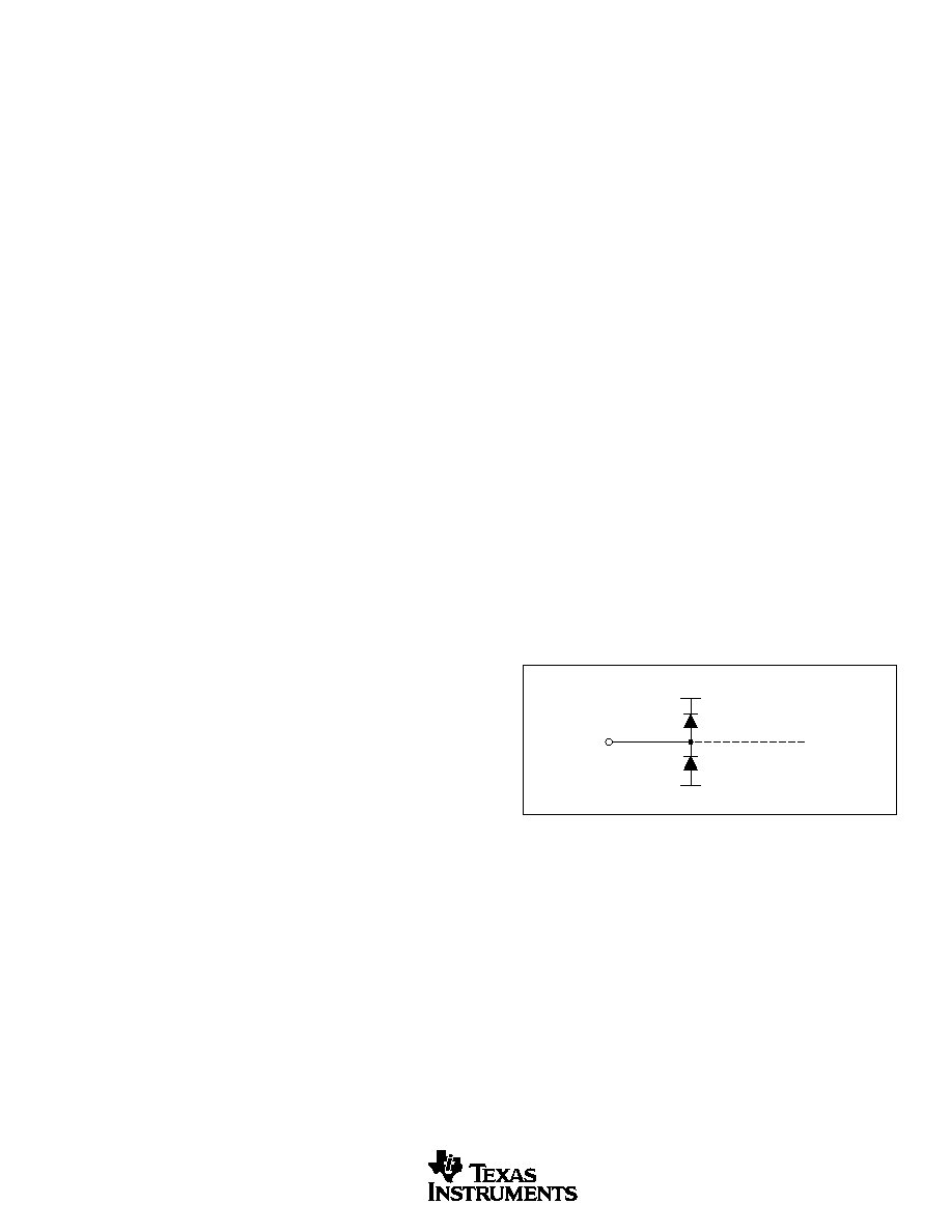
INPUT AND ESD PROTECTION
The OPA2631 is built using a very high-speed complemen-
tary bipolar process. The internal junction breakdown volt-
ages are relatively low for this very small geometry device.
This breakdown is reflected in the Absolute Maximum
Ratings table. All device pins are protected with internal
ESD protection diodes to the power supplies, as shown in
Figure 9.
These diodes provide moderate protection to input overdrive
External
Pin
+V
CC
≠V
CC
Internal
Circuitry
FIGURE 9. Internal ESD Protection.
voltages above the supplies as well. The protection diodes
can typically support 30mA continuous current. Where higher
currents are possible (e.g., in systems with
±
15V supply
parts driving into the OPA2631), current-limiting series
resistors should be added into the two inputs. Keep these
resistor values as low as possible, since high values degrade
both noise performance and frequency response.

PACKAGING INFORMATION
ORDERABLE DEVICE
STATUS(1)
PACKAGE TYPE
PACKAGE DRAWING
PINS
PACKAGE QTY
OPA2631U
OBSOLETE
SOIC
D
8
OPA2631U/2K5
OBSOLETE
SOIC
D
8
(1) The marketing status values are defined as follows:
ACTIVE: Product device recommended for new designs.
LIFEBUY: TI has announced that the device will be discontinued, and a lifetime-buy period is in effect.
NRND: Not recommended for new designs. Device is in production to support existing customers, but TI does not recommend using this part in
a new design.
PREVIEW: Device has been announced but is not in production. Samples may or may not be available.
OBSOLETE: TI has discontinued the production of the device.
PACKAGE OPTION ADDENDUM
www.ti.com
3-Oct-2003

IMPORTANT NOTICE
Texas Instruments Incorporated and its subsidiaries (TI) reserve the right to make corrections, modifications,
enhancements, improvements, and other changes to its products and services at any time and to discontinue
any product or service without notice. Customers should obtain the latest relevant information before placing
orders and should verify that such information is current and complete. All products are sold subject to TI's terms
and conditions of sale supplied at the time of order acknowledgment.
TI warrants performance of its hardware products to the specifications applicable at the time of sale in
accordance with TI's standard warranty. Testing and other quality control techniques are used to the extent TI
deems necessary to support this warranty. Except where mandated by government requirements, testing of all
parameters of each product is not necessarily performed.
TI assumes no liability for applications assistance or customer product design. Customers are responsible for
their products and applications using TI components. To minimize the risks associated with customer products
and applications, customers should provide adequate design and operating safeguards.
TI does not warrant or represent that any license, either express or implied, is granted under any TI patent right,
copyright, mask work right, or other TI intellectual property right relating to any combination, machine, or process
in which TI products or services are used. Information published by TI regarding third-party products or services
does not constitute a license from TI to use such products or services or a warranty or endorsement thereof.
Use of such information may require a license from a third party under the patents or other intellectual property
of the third party, or a license from TI under the patents or other intellectual property of TI.
Reproduction of information in TI data books or data sheets is permissible only if reproduction is without
alteration and is accompanied by all associated warranties, conditions, limitations, and notices. Reproduction
of this information with alteration is an unfair and deceptive business practice. TI is not responsible or liable for
such altered documentation.
Resale of TI products or services with statements different from or beyond the parameters stated by TI for that
product or service voids all express and any implied warranties for the associated TI product or service and
is an unfair and deceptive business practice. TI is not responsible or liable for any such statements.
Following are URLs where you can obtain information on other Texas Instruments products and application
solutions:
Products
Applications
Amplifiers
amplifier.ti.com
Audio
www.ti.com/audio
Data Converters
dataconverter.ti.com
Automotive
www.ti.com/automotive
DSP
dsp.ti.com
Broadband
www.ti.com/broadband
Interface
interface.ti.com
Digital Control
www.ti.com/digitalcontrol
Logic
logic.ti.com
Military
www.ti.com/military
Power Mgmt
power.ti.com
Optical Networking
www.ti.com/opticalnetwork
Microcontrollers
microcontroller.ti.com
Security
www.ti.com/security
Telephony
www.ti.com/telephony
Video & Imaging
www.ti.com/video
Wireless
www.ti.com/wireless
Mailing Address:
Texas Instruments
Post Office Box 655303 Dallas, Texas 75265
Copyright
2003, Texas Instruments Incorporated