1
Æ
OPA2650
FEATURES
q
LOW POWER: 50mW/Chan.
q
UNITY GAIN STABLE BANDWIDTH:
360MHz
q
FAST SETTLING TIME: 20ns to 0.01%
q
LOW HARMONICS: ≠77dBc at 5MHz
q
DIFFERENTIAL GAIN/PHASE ERROR:
0.01%/0.025
∞
q
HIGH OUTPUT CURRENT: 85mA
DESCRIPTION
The OPA2650 is a dual, low power, wideband voltage
feedback operational amplifier. It features a high band-
width of 360MHz as well as a 12-bit settling time of
only 20ns. The low distortion allows its use in commu-
nications applications, while the wide bandwidth and
true differential input stage make it suitable for use in
a variety of active filter applications. Its low distortion
gives exceptional performance for telecommunica-
tions, medical imaging and video applications.
The OPA2650 is internally compensated for unity-
gain stability. This amplifier has a fully symmetrical
differential input due to its "classical" operational
amplifier circuit architecture. Its unusual combination
of speed, accuracy and low power make it an outstand-
ing choice for many portable, multi-channel and other
high speed applications, where power is at a premium.
The OPA2650 is also available in single (OPA650)
and quad (OPA4650) configurations.
Dual Wideband, Low Power Voltage Feedback
OPERATIONAL AMPLIFIER
© 1994 Burr-Brown Corporation
PDS-1266C
Printed in U.S.A. June, 1997
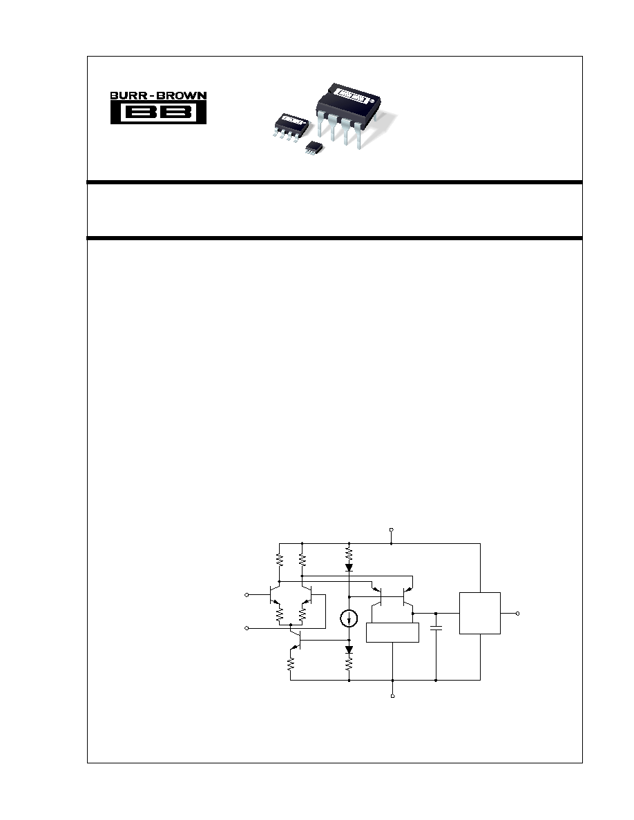
NOTE: Diagram shows only one-half of the OPA2650.
APPLICATIONS
q
HIGH RESOLUTION VIDEO
q
BASEBAND AMPLIFIER
q
CCD IMAGING AMPLIFIER
q
ULTRASOUND SIGNAL PROCESSING
q
ADC/DAC GAIN AMPLIFIER
q
ACTIVE FILTERS
q
HIGH SPEED INTEGRATORS
q
DIFFERENTIAL AMPLIFIER
Current
Mirror
Output
Stage
C
C
Inverting
Input
Non-Inverting
Input
+V
S
Output
≠V
S
International Airport Industrial Park ∑ Mailing Address: PO Box 11400, Tucson, AZ 85734 ∑ Street Address: 6730 S. Tucson Blvd., Tucson, AZ 85706 ∑ Tel: (520) 746-1111 ∑ Twx: 910-952-1111
Internet: http://www.burr-brown.com/ ∑ FAXLine: (800) 548-6133 (US/Canada Only) ∑ Cable: BBRCORP ∑ Telex: 066-6491 ∑ FAX: (520) 889-1510 ∑ Immediate Product Info: (800) 548-6132
OPA2650
OPA2650
Æ
OPA2650
SBOS043
2
Æ
OPA2650
NOTES: (1) An asterisk (
T
) specifies the same value as the grade to the left. (2) Frequency response can be strongly influenced by PC board parasitics. The
demonstration boards show low parasitic layouts for this part. Refer to the demonstration board layout for details. (3) Slew rate is rate of change from 10% to 90%
of output voltage step.
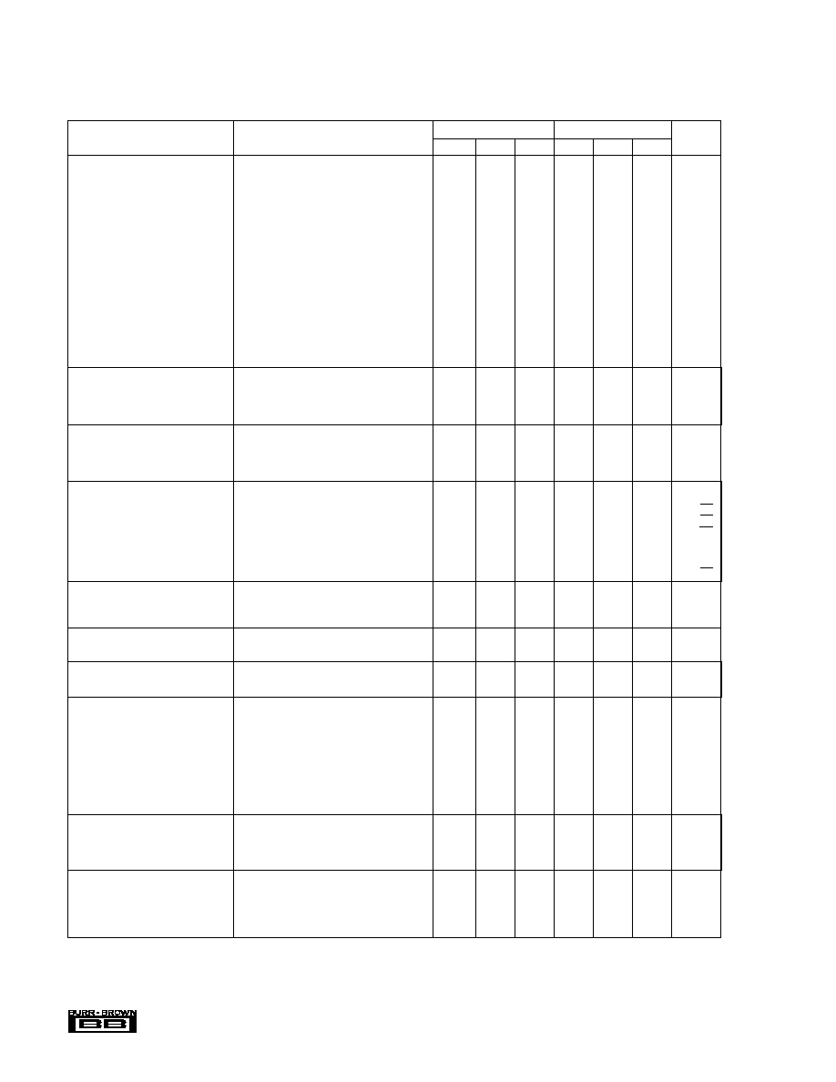
SPECIFICATIONS
At T
A
= +25
∞
C, V
S
=
±
5V, R
L
= 100
, and R
FB
= 402
,
unless otherwise noted. R
FB
= 25
for a gain of +1.
OPA2650P, U, E
OPA2650PB, UB
PARAMETER
CONDITIONS
MIN
TYP
MAX
MIN
TYP
MAX
UNITS
FREQUENCY RESPONSE
Closed-Loop Bandwidth
(2)
G = +1
360
T
(1)
MHz
G = +2
108
T
MHz
G = +5
32
T
MHz
G = +10
16
T
MHz
Gain Bandwidth Product
G
+5
160
MHz
Bandwidth for 0.1dB Flatness
(2)
G = +2
21
T
MHz
Slew Rate
(3)
G = +1, 2V Step
240
T
V/
µ
s
Over Temperature Range
220
T
V/
µ
s
Rise Time
G = +1, 0.2V Step
1
T
ns
Fall Time
G = +1, 0.2V Step
1
T
ns
Settling Time
0.01%
G = +1, 2V Step
20
T
ns
0.1%
G = +1, 2V Step
11
T
ns
1%
G = +1, 2V Step
6.7
T
ns
Spurious Free Dynamic Range
G = +1, f = 5.0MHz, V
O
= 2Vp-p
R
L
= 100
72
T
dB
R
L
= 402
77
T
dB
Differential Gain
G = +2, NTSC, V
O
= 1.4Vp-p, R
L
= 150
0.01
T
%
Differential Phase
G = +2, NTSC, V
O
= 1.4Vp-p, R
L
= 150
0.025
T
Degrees
Crosstalk
(2)
Input Referred, 5MHz, Channel-to-Channel
≠84
T
dB
INPUT OFFSET VOLTAGE
Input Offset Voltage
V
CM
= 0V
±
1
±
5
±
1
±
3
mV
Average Drift
±
3
T
µ
V/
∞
C
Power Supply Rejection (+V
S
)
Input Referred, V
S
=
±
4.5V to
±
5.5V
60
76
70
T
dB
(≠V
S
)
47
54
50
T
dB
INPUT BIAS CURRENT
Input Bias Current
V
CM
= 0V
5
20
T
10
µ
A
Over Temperature Range
30
20
µ
A
Input Offset Current
V
CM
= 0V
0.5
1
0.2
0.5
µ
A
Over Temperature Range
3
2
µ
A
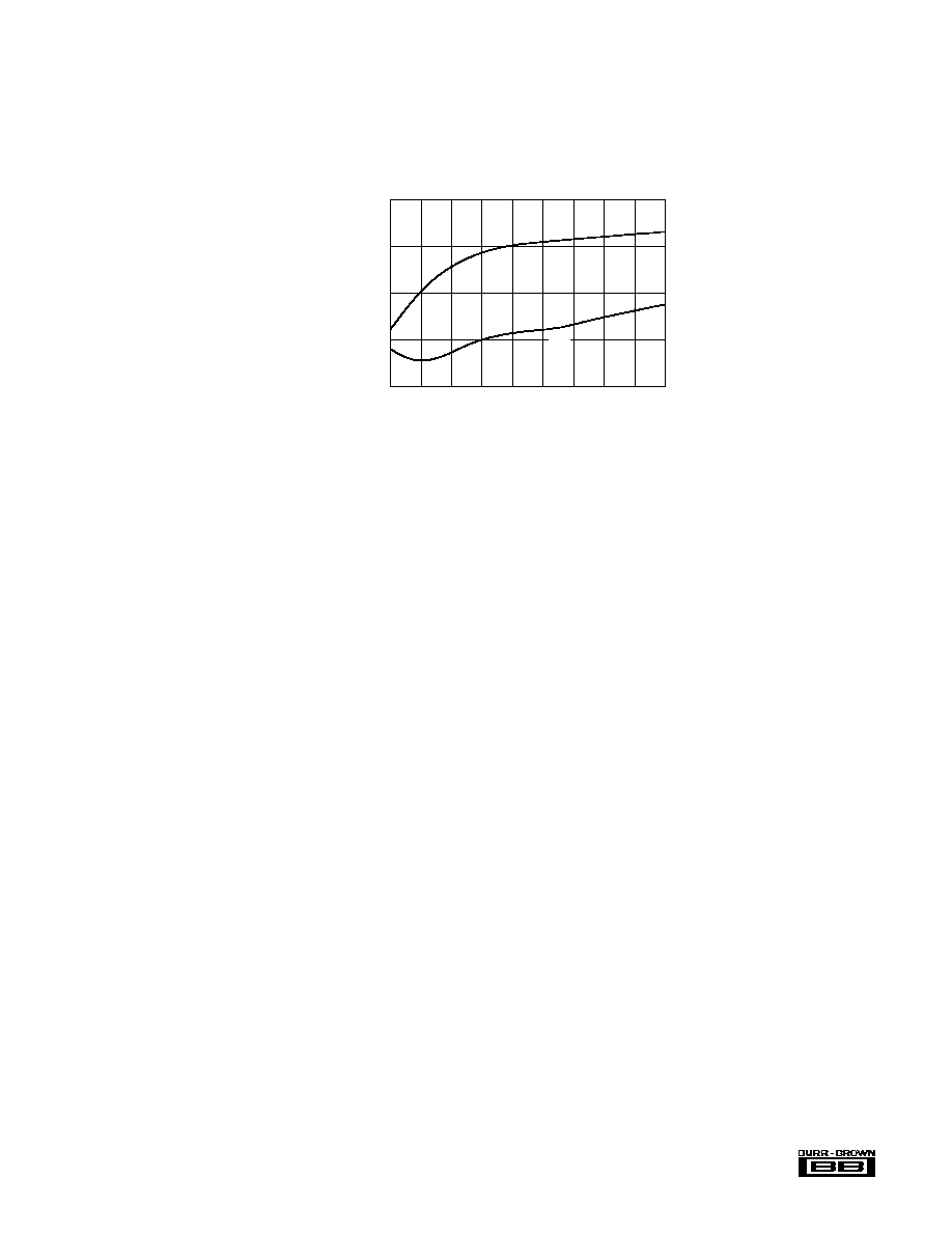
INPUT NOISE
Input Voltage Noise
Noise Density, f = 100Hz
43
T
nV/
Hz
f = 10kHz
9.4
T
nV/
Hz
f
1MHz
8.4
T
nV/
Hz
Integrated Noise
f
B
= 10Hz to 100MHz
84
T
µ
Vrms
Input Bias Current Noise
Noise Density, f
0.1MHz
1.2
T
pA/
Hz
INPUT VOLTAGE RANGE
Common-Mode Input Range
±
2.8
T
V
Over Temperature Range
±
2.2
T
V
Common-Mode Rejection
Input Referred, V
CM
=
±
0.5V
65
90
70
T
dB
INPUT IMPEDANCE
Differential
15 || 1
T
K
|| pF
Common-Mode
16 || 1
T
M
|| pF
OPEN-LOOP GAIN
Open-Loop Voltage Gain
V
O
=
±
2V, R
L
= 100
45
51
47
T
dB
Over Temperature Range
43
45
dB
OUTPUT
Voltage Output
Over Temperature Range
No Load
±
2.2
±
3.0
±
2.4
T
V
R
L
= 250
±
2.2
±
2.5
±
2.4
T
V
R
L
= 100
±
2.0
±
2.3
±
2.2
T
V
Output Current, Sourcing
75
110
T
T
mA
Over Temperature Range
65
T
mA
Output Current, Sinking
65
85
T
T
mA
Over Temperature Range
35
T
mA
Short Circuit Current
150
T
mA
Output Resistance
f < 100kHz, G = +1
0.08
T
POWER SUPPLY
Specified Operating Voltage
±
5
T
V
Operating Voltage Range
±
4.5
±
5.5
T
T
V
Quiescent Current
Both Channels, V
S
=
±
5V
±
11
±
15.5
T
±
13.5
mA
Over Temperature Range
±
17.5
T
±
16
mA
THERMAL CHARACTERISTICS
Temperature Range
Specification: P, U, E, PB, UB
≠40
+85
T
T
∞
C
Thermal Resistance,
JA
Junction to Ambient
P
8-Pin DIP
100
T
∞
C/W
U
SO-8
125
T
∞
C/W
E
MSOP-8
150
T
∞
C/W

3
Æ
OPA2650
Supply Voltage .................................................................................
±
5.5V
Internal Power Dissipation ........................... See Thermal Characteristics
Differential Input Voltage ..................................................................
±
1.2V
Input Voltage Range ............................................................................
±
V
S
Storage Temperature Range: P, PB, U, UB, E ............ ≠40
∞
C to +125
∞
C
Lead Temperature (DIP, soldering, 10s) ...................................... +300
∞
C
(SO-8 and MSOP-8, soldering, 3s) ................ +260
∞
C
Junction Temperature (T
J
) ............................................................ +175
∞
C
ABSOLUTE MAXIMUM RATINGS
Top View
DIP/SO-8/MSOP-8
PIN CONFIGURATION
+V
S
Output
2
≠Input
2
+Input
2
Output
1
≠Input
1
+Input
1
≠V
S
1
2
3
4
8
7
6
5
The information provided herein is believed to be reliable; however, BURR-BROWN assumes no responsibility for inaccuracies or omissions. BURR-BROWN assumes no responsibility for the use
of this information, and all use of such information shall be entirely at the user's own risk. Prices and specifications are subject to change without notice. No patent rights or licenses to any of the
circuits described herein are implied or granted to any third party. BURR-BROWN does not authorize or warrant any BURR-BROWN product for use in life support devices and/or systems.
ELECTROSTATIC
DISCHARGE SENSITIVITY
Electrostatic discharge can cause damage ranging from per-
formance degradation to complete device failure. Burr-Brown
Corporation recommends that all integrated circuits be handled
and stored using appropriate ESD protection methods.
ESD damage can range from subtle performance degradation
to complete device failure. Precision integrated circuits may
be more susceptible to damage because very small parametric
changes could cause the device not to meet published speci-
fications.
PACKAGE
DRAWING
TEMPERATURE
PACKAGE
ORDERING
PRODUCT
PACKAGE
NUMBER
(1)
RANGE
MARKING
(2)
NUMBER
(3)
OPA2650P
8-Pin Plastic DIP
006
≠40
∞
C to +85
∞
C
OPA2650P
OPA2650P
OPA2650PB
8-Pin Plastic DIP
006
≠40
∞
C to +85
∞
C
OPA2650PB
OPA2650PB
OPA2650U
SO-8 Surface Mount
182
≠40
∞
C to +85
∞
C
OPA2650U
OPA2650U
OPA2650UB
SO-8 Surface Mount
182
≠40
∞
C to +85
∞
C
OPA2650UB
OPA2650UB
OPA2650E
MSOP-8
337
≠40
∞
C to +85
∞
C
B50
OPA2650E-250
OPA2650E-2500
NOTE: (1) For detailed drawing and dimension table, see end of data sheet, or Appendix C of Burr-Brown IC Data Book. (2) The "B" grade will be marked with a "B"
by pin 8. (3) The MSOP-8 is available on 7" tape and reel with 250 parts, and on 14" tape and reel with 2500 parts. For example, ordering 250 pieces of "OPA2650E-
250" will get a single 250 piece tape and reel. Refer to Appendix B of Burr-Brown IC Data Book for detailed Tape and Reel Mechanical information.
PACKAGE/ORDERING INFORMATION

4
Æ
OPA2650
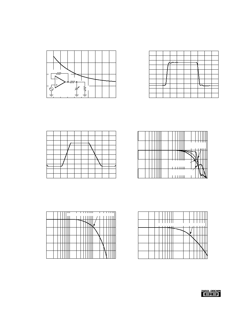
TYPICAL PERFORMANCE CURVES
At T
A
= +25
∞
C, V
S
=
±
5V, R
L
= 100
, and R
FB
= 402
,
unless otherwise noted. R
FB
= 25
for a gain of +1.
INPUT VOLTAGE AND CURRENT NOISE
vs FREQUENCY
Frequency (Hz)
100
1k
10k
100k
1M
100
10
1
Input Current Noise (pA/
Hz)
Input Voltage Noise (nV/
Hz)
Non-inverting and
Inverting Current Noise
Voltage Noise
COMMON-MODE REJECTION
vs INPUT COMMON-MODE VOLTAGE
100
90
80
70
60
≠4
≠3
≠2
≠1
0
1
2
3
4
Common Mode-Rejection (dB)
Common-Mode Voltage (V)
A
OL
, PSR AND CMRR vs TEMPERATURE
100
90
80
70
60
50
40
≠50
≠25
0
25
50
75
125
A
OL
, PSR and CMRR (dB)
Temperature (∞C)
A
OL
PSR≠
CMRR
PSR+
INPUT BIAS CURRENT vs TEMPERATURE
6
5
4
3
3
2
1
0
≠50
≠25
0
25
50
75
100
Input Bias Current (µA)
Offset Voltage (mV)
Temperature (∞C)
I
B
V
OS
SUPPLY CURRENT vs TEMPERATURE
12
11
10
9
≠75
≠50
≠25
0
25
50
75
100
125
Supply Current (mA)
Temperature (∞C)
I
Q
OUTPUT CURRENT vs TEMPERATURE
110
100
90
80
70
≠50
≠25
0
25
50
75
100
Outrput Current (±mA)
Temperature (∞C)
I
O
≠
I
O
+
5
Æ
OPA2650
TYPICAL PERFORMANCE CURVES
(CONT)
At T
A
= +25
∞
C, V
S
=
±
5V, R
L
= 100
, and R
FB
= 402
,
unless otherwise noted. R
FB
= 25
for a gain of +1.
LARGE SIGNAL TRANSIENT RESPONSE
(G = +1)
Time (5ns/div)
2.0
1.6
1.2
0.8
0.4
0
≠0.4
≠0.8
≠1.2
≠1.6
≠2.0
Output Voltage (V)
SMALL SIGNAL TRANSIENT RESPONSE
(G = +1)
Time (5ns/div)
200
160
120
80
40
0
≠40
≠80
≠120
≠160
≠200
Output Voltage (mV)
RECOMMENDED ISOLATION RESISTANCE
vs CAPACITIVE LOAD
40
30
20
10
0
0
20
40
60
80
100
Isolation Resistance, R
ISO
(
)
Capacitive Load, C
L
(pF)
OPA2650
C
L
1k
R
ISO
25
CLOSED-LOOP BANDWIDTH (G = +1)
Frequency (Hz)
6
3
0
≠3
≠6
≠9
1M
10M
100M
1G
Gain (dB)
DIP Bandwidth
= 366MHz
SO-8 Bandwidth
= 331MHz
MSOP-8 Bandwidth
= 281MHz
CLOSED-LOOP BANDWIDTH (G = +2)
Frequency (Hz)
9
6
3
0
≠3
≠6
≠9
1M
10M
100M
1G
MSOP-8/SO-8/DIP Bandwidth = 108MHz
Gain (dB)
CLOSED-LOOP BANDWIDTH (G = +5)
Frequency (Hz)
20
17
14
11
8
5
2
1M
10M
100M
MSOP-8/SO-8/DIP Bandwidth = 31MHz
Gain (dB)

6
Æ
OPA2650
TYPICAL PERFORMANCE CURVES
(CONT)
At T
A
= +25
∞
C, V
S
=
±
5V, R
L
= 100
, and R
FB
= 402
,
unless otherwise noted. R
FB
= 25
for a gain of +1.
OPEN-LOOP GAIN AND PHASE
vs FREQUENCY
60
50
40
30
20
10
0
+45
0
≠45
≠90
≠135
≠180
≠225
1k
10k
100k
1M
10M
100M
1G
Gain (dB)
Phase (∞)
Frequency (Hz)
Phase
Gain
HARMONIC DISTORTION vs FREQUENCY
(G = +1, V
O
= 2Vp-p)
≠45
≠50
≠55
≠60
≠65
≠70
≠75
≠80
≠85
≠90
≠95
100k
1M
3f
O
2f
O
10M
100M
Harmonic Distortion (dBc)
Frequency (Hz)
HARMONIC DISTORTION
vs TEMPERATURE (G = +1, f
O
= 5MHz)
≠60
≠65
≠70
≠75
≠80
≠75
≠50
≠25
0
25
50
75
100
125
Harmonic Distortion (dBc)
Temperature (∞C)
3f
O
2f
O
5MHz HARMONIC DISTORTION
vs OUTPUT SWING
Output Swing (Vp-p)
≠60
≠70
≠80
≠90
≠100
0.1
1
10
Harmonic Distortion (dBc)
3f
O
2f
O
G = +2
CLOSED-LOOP BANDWIDTH (G = +10)
Frequency (Hz)
26
23
20
17
14
11
8
5
2
1M
10M
100M
MSOP-8/SO-8/DIP Bandwidth = 16MHz
Gain (dB)
10MHz HARMONIC DISTORTION
vs OUTPUT SWING
Output Swing (Vp-p)
≠50
≠60
≠70
≠80
≠90
0.1
1
10
Harmonic Distortion (dBc)
3f
O
2f
O
G = +2
7
Æ
OPA2650
APPLICATIONS INFORMATION
DISCUSSION OF PERFORMANCE
The OPA2650 is a dual low power, wideband voltage feed-
back operational amplifier. Each channel is internally com-
pensated to provide unity gain stability. The OPA2650's
voltage feedback architecture features true differential and
fully symmetrical inputs. This minimizes offset errors, mak-
ing the OPA2650 well suited for implementing filter and
instrumentation designs. As a dual operational amplifier,
OPA2650 is an ideal choice for designs requiring multiple
channels where reduction of board space, power dissipation
and cost are critical. Its AC performance is optimized to
provide a gain bandwidth product of 160MHz and a fast 0.1%
settling time of 11ns, which is an important consideration in
high speed data conversion applications. Along with its
excellent settling characteristics, the low DC input offset of
±
1mV and drift of
±
3
µ
V/
∞
C support high accuracy require-
ments. In applications requiring a higher slew rate and wider
bandwidth, such as video and high bit rate digital communi-
cations, consider the dual current feedback OPA2658.
CIRCUIT LAYOUT AND BASIC OPERATION
Achieving optimum performance with a high frequency am-
plifier like the OPA2650 requires careful attention to layout
parasitics and selection of external components. Recommen-
dations for PC board layout and component selection include:
a) Minimize parasitic capacitance to any ac ground for all
of the signal I/O pins. Parasitic capacitance on the output
and inverting input pins can cause instability; on the non-
inverting input it can react with the source impedance to
cause unintentional bandlimiting. To reduce unwanted ca-
pacitance, a window around the signal I/O pins should be
opened in all of the ground and power planes. Otherwise,
ground and power planes should be unbroken elsewhere on
the board.
b) Minimize the distance (< 0.25") from the two power pins
to high frequency 0.1
µ
F decoupling capacitors. At the pins,
the ground and power plane layout should not be in close
proximity to the signal I/O pins. Avoid narrow power and
ground traces to minimize inductance between the pins and
the decoupling capacitors. Larger (2.2
µ
F to 6.8
µ
F) decoupling
capacitors, effective at lower frequencies, should also be
used. These may be placed somewhat farther from the
device and may be shared among several devices in the same
area of the PC board.
c) Careful selection and placement of external compo-
nents will preserve the high frequency performance of the
OPA2650. Resistors should be a very low reactance type.
Surface mount resistors work best and allow a tighter overall
layout. Metal film or carbon composition axially-leaded
resistors can also provide good high frequency performance.
Again, keep their leads as short as possible. Never use
wirewound type resistors in a high frequency application.
Since the output pin and the inverting input pin are most
sensitive to parasitic capacitance, always position the feed-
back and series output resistor, if any, as close as possible to
the package pins. Other network components, such as non-
inverting input termination resistors, should also be placed
close to the package.
Even with a low parasitic capacitance shunting the resistor,
excessively high resistor values can create significant time
constants and degrade performance. Good metal film or
surface mount resistors have approximately 0.2pF in shunt
with the resistor. For resistor values > 1.5k
, this adds a
pole and/or zero below 500MHz that can affect circuit
TYPICAL PERFORMANCE CURVES
(CONT)
At T
A
= +25
∞
C, V
S
=
±
5V, R
L
= 100
, and R
FB
= 402
,
unless otherwise noted. R
FB
= 25
for a gain of +1.
HARMONIC DISTORTION vs GAIN
(f = 5MHZ, V
O
= 2Vp-p)
≠40
≠50
≠60
≠70
≠80
1
2
3
4
5
6
7
8
9
10
Harmonic Distortion (dBc)
Non-Inverting Gain (V/V)
3f
O
2f
O
8
Æ
OPA2650
operation. Keep resistor values as low as possible consistent
with output loading considerations. The 402
feedback
used for the Typical Performance Plots is a good starting
point for design. Note that a 25
feedback resistor, rather
than a direct short, is suggested for a unity gain follower.
This effectively reduces the Q of what would otherwise be
a parasitic inductance (the feedback wire) into the parasitic
capacitance at the inverting input.
d) Connections to other wideband devices on the board
may be made with short direct traces or through on-board
transmission lines. For short connections, consider the trace
and the input to the next device as a lumped capacitive load.
Relatively wide traces (50 to 100 mils) should be used,
preferably with ground and power planes opened up around
them. Estimate the total capacitive load and set R
ISO
from
the plot of recommended R
ISO
vs capacitive load. Low
parasitic loads may not need an R
ISO
since the OPA2650 is
nominally compensated to operate with a 2pF parasitic load.
If a long trace is required and the 6dB signal loss intrinsic to
doubly terminated transmission lines is acceptable, imple-
ment a matched impedance transmission line using microstrip
or stripline techniques (consult an ECL design handbook for
microstrip and stripline layout techniques). A 50
environ-
ment is not necessary on board, and in fact a higher imped-
ance environment will improve distortion as shown in the
distortion vs load plot. With a characteristic impedance
defined based on board material and desired trace dimen-
sions, a matching series resistor into the trace from the
output of the amplifier is used as well as a terminating shunt
resistor at the input of the destination device. Remember
also that the terminating impedance will be the parallel
combination of the shunt resistor and the input impedance of
the destination device; the total effective impedance should
match the trace impedance. Multiple destination devices are
best handled as separate transmission lines, each with their
own series and shunt terminations.
If the 6dB attenuation loss of a doubly terminated line is
unacceptable, a long trace can be series-terminated at the
source end only. This will help isolate the line capacitance
from the op amp output, but will not preserve signal integrity
as well as a doubly terminated line. If the shunt impedance
at the destination end is finite, there will be some signal
attenuation due to the voltage divider formed by the series
and shunt impedances.
e) Sockets are not recommended for high speed parts like
the OPA2650. The additional lead length and pin-to-pin
capacitance introduced by the socket creates an extremely
troublesome parasitic network which can make it almost
impossible to achieve a smooth, stable response. Best results
are obtained by soldering the part onto the board. If socket-
ing for the DIP package is desired, high frequency flush
mount pins (e.g., McKenzie Technology #710C) can give
good results.
SUPPLY VOLTAGES
The OPA2650 is nominally specified for operation using
±
5V
power supplies. A 10% tolerance on the supplies, or an ECL
≠5.2V for the negative supply, is within the maximum speci-
fied total supply voltage of 11V. Higher supply voltages can
break down internal junctions possibly leading to catastrophic
failure. Single supply operation is possible as long as com-
mon mode voltage constraints are observed. The common
mode input and output voltage specifications can be inter-
preted as a required headroom to the supply voltage. Observ-
ing this input and output headroom requirement will allow
non-standard or single supply operation. Figure 1 shows one
approach to single-supply operation.
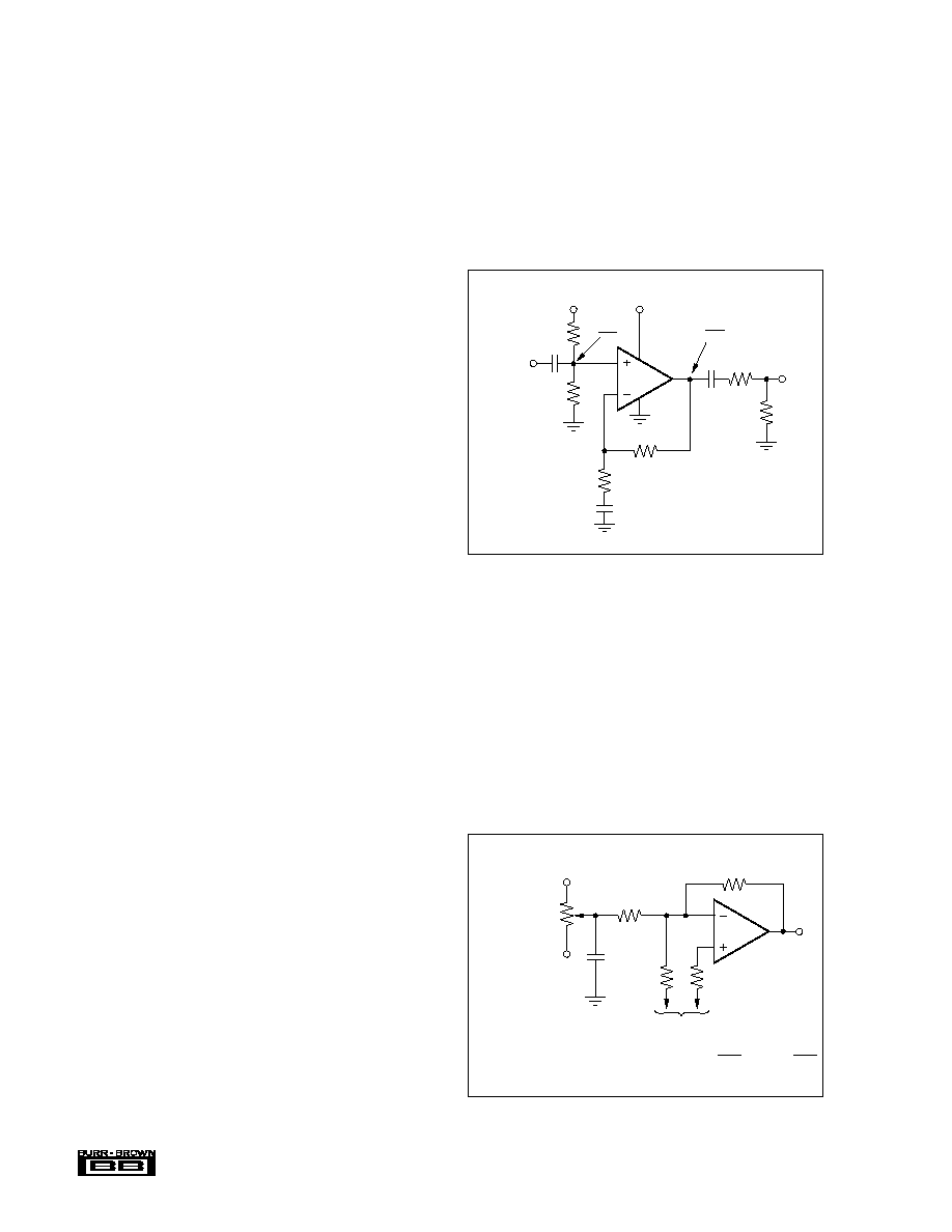
FIGURE 2. Offset Voltage Trim.
OFFSET VOLTAGE ADJUSTMENT
If additional offset adjustment is needed, the circuit in
Figure 2 can be used without degrading offset drift with
temperature. Avoid external adjustment whenever possible
since extraneous noise, such as power supply noise, can be
inadvertently coupled into the amplifier's inverting input
terminal. Remember that additional offset errors can be
created by the amplifier's input bias currents. Whenever
possible, match the impedance seen by both inputs as is
shown with R
3
. This will reduce the output offset voltage
caused by the amplifier's input offset current.
FIGURE 1. Single Supply Operation.
R
2
1/2
OPA2650
(1)
R
3
= R
1
|| R
2
R
1
R
Trim
+V
CC
≠V
CC
20k
V
IN
or Ground
Output Trim Range +V
CC
to ≠V
CC
NOTE: (1) R
3
is
optional and can
be used to cancel
offset errors due
to input bias currents.
R
Trim
47k
R
2
R
2
R
Trim
0.1µF
402
1/2
OPA2650
V
AC
R
R
402
R
L
+V
S
+V
S
V
S
2
R
OUT
V
S
2
V
OUT
= + 2∑V
AC

9
Æ
OPA2650
ESD PROTECTION
ESD damage has been well recognized for MOSFET de-
vices, but any semiconductor device is vulnerable to this
potentially damaging source. This is particularly true for
very high speed, fine geometry processes.
ESD damage can cause subtle changes in amplifier input
characteristics without necessarily destroying the device. In
precision operational amplifiers, this may cause a noticeable
degradation of offset voltage and drift. Therefore, ESD
handling precautions are strongly recommended when han-
dling the OPA2650.
OUTPUT DRIVE CAPABILITY
The OPA2650 has been optimized to drive 75
and 100
resistive loads. The device can drive 2Vp-p into a 75
load. This high-output drive capability makes the OPA2650
an ideal choice for a wide range of RF, IF, and video
applications. In many cases, additional buffer amplifiers
are unneeded.
Many demanding high-speed applications such as driving
A/D converters require op amps with low wideband output
impedance. For example, low output impedance is essential
when driving the signal-dependent capacitances at the inputs
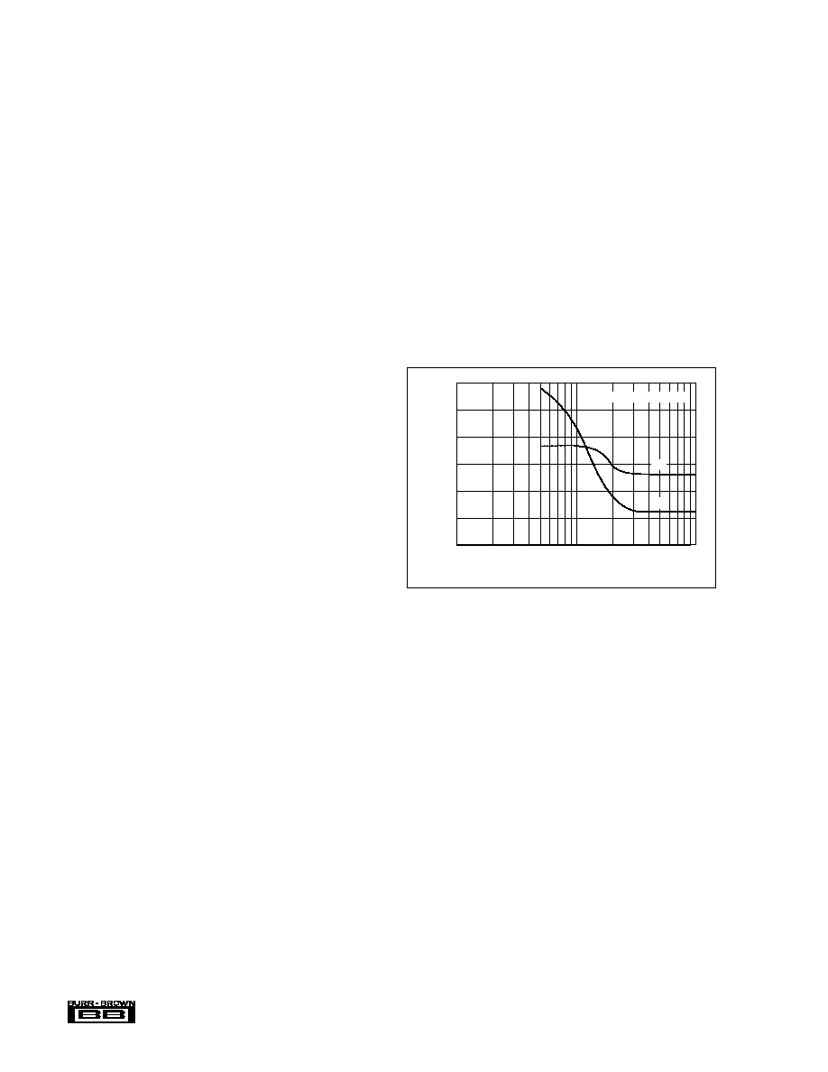
of flash A/D converters. As shown in Figure 3, the OPA2650
maintains very low-closed loop output impedance over fre-
quency. Closed-loop output impedance increases with fre-
quency since loop gain decreases with frequency.
supply current for both channels times the total supply
voltage across the part. P
DL1
and P
DL2
will depend on the
required output signals and loads. For a grounded resistive
loads, and equal bipolar supplies, they would be at a
maximum when the outputs are fixed at a voltage equal to
1/2 either supply voltage. Under this condition, P
DL1
= V
S
2
/
(4∑R
L1
) where R
L1
includes feedback network loading. P
DL2
is calculated the same way.
Note that it is the power in the output stages, and not into
the loads, that determines internal power dissipation.
Operating junction temperature (T
J
) is given by T
A
+ P
D
JA
, where T
A
is the ambient temperature.
As an example, compute the maximum T
J
for an OPA2650U
where both op amps are at G = +2, R
L
= 100
, R
FB
= 402
,
±
V
S
=
±
5V, and at the specified maximum T
A
= +85
∞
C.
This gives:
CAPACITIVE LOADS
The OPA2650's output stage has been optimized to drive low
resistive loads. Capacitive loads, however, will decrease the
amplifier's phase margin which may cause high frequency
peaking or oscillations. Capacitive loads greater than 10pF
should be isolated by connecting a small resistance, usually
15
to 30
, in series with the output as shown in Figure 4.
This is particularly important when driving high capacitance
loads such as flash A/D converters. Increasing the gain from
+1 will improve the capacitive load drive due to increased
phase margin.
In general, capacitive loads should be minimized for opti-
mum high frequency performance. Coax lines can be driven
if the cable is properly terminated. The capacitance of coax
cable (29pF/foot for RG-58) will not load the amplifier
when the coaxial cable or transmission line is terminated in
its characteristic impedance.
FIGURE 3. Small-Signal Output Impedance vs Frequency.
SMALL-SIGNAL OUTPUT IMPEDANCE
vs FREQUENCY
Frequency (Hz)
1k
100
10
1
0.1
0.01
10k
100k
1M
100M
10M
Output Impedance (
)
G = +1
THERMAL CONSIDERATIONS
The OPA2650 will not require heatsinking under most
operating conditions. Maximum desired junction tempera-
ture will set a maximum allowed internal power dissipation
as described below. In no case should the maximum junction
temperature be allowed to exceed 175
∞
C.
The total internal power dissipation (P
D
) is a the sum of
quiescent power (P
DQ
) and additional power dissipated in
the two output stages (P
DL1
and P
DL2
) while delivering load
power. Quiescent power is simply the specified no-load
FIGURE 4. Driving Capacitive Loads.
OPA2650
C
L
R
L
R
ISO
(R
ISO
typically 15
to 30
)
25
P
DQ
=
10V ∑ 17. 5mA
(
)
=
175mW
P
DL1
=
P
DL 2
=
5V
( )
2
4 ∑ 100
|| 804
(
)
=
70mW
P
D
=
175mW
+
2 70mW
(
)
=
315mW
T
J
=
85
∞
C
+
0.315W ∑ 125
∞
C / W
=
124
∞
C
10
Æ
OPA2650
FREQUENCY RESPONSE COMPENSATION
Each channel of the OPA2650 is internally compensated to
be stable at unity gain with a nominal 60
∞
phase margin.
This lends itself well to wideband integrator and buffer
applications. Phase margin and frequency response flatness
will improve at higher gains. Recall that an inverting gain of
≠1 is equivalent to a gain of +2 for bandwidth purposes, i.e.,
noise gain = 2. The external compensation techniques devel-
oped for voltage feedback op amps can be applied to this
device. For example, in the non-inverting configuration,
placing a capacitor across the feedback resistor will reduce
the gain to +1 starting at f = (1/2
R
F
C
F
). Alternatively, in the
inverting configuration, the bandwidth may be limited with-
out modifying the inverting gain by placing a series RC
network to ground on the inverting node. This has the effect
of increasing the noise gain at high frequencies, thereby
limiting the bandwidth for the inverting input signal through
the gain-bandwidth product.
At higher gains, the gain-bandwidth of this voltage feedback
topology will limit bandwidth according to the open-loop
frequency response curve. For applications requiring a wider
bandwidth at higher gains, consider the dual current feed-
back model, OPA2658. In applications where a large feed-
back resistor is required (such as photodiode transimpedance
circuits), precautions must be taken to avoid gain peaking
due to the pole formed by the feedback resistor and the
capacitance on the inverting input. This pole can be compen-
sated by connecting a small capacitor in parallel with the
feedback resistor, creating a cancelling zero term. In other
high-gain applications, use of a three-resistor "T" connec-
tion will reduce the feedback network impedance which
reacts with the parasitic capacitance at the summing node.
PULSE SETTLING TIME
High speed amplifiers like the OPA2650 are capable of
extremely fast settling time with a pulse input. Excellent
frequency response flatness and phase linearity are required
to get the best settling times. As shown in the specifications
table, settling time for a
2
V step at a gain of +1 for the
OPA2650 is extremely fast. The specification is defined as
the time required, after the input transition, for the output to
settle within a specified error band around its final value. For
a 2V step, 1% settling corresponds to an error band of
±
20mV, 0.1% to an error band of
±
2mV, and 0.01% to an
error band of
±
0.2mV. For the best settling times, particu-
larly into an ADC capacitive load, little or no peaking in the
frequency response can be allowed. Using the recommended
R
ISO
for capacitive loads will limit this peaking and reduce
the settling times. Fast, extremely fine scale settling (0.01%)
requires close attention to ground return currents in the
supply decoupling capacitors. For highest performance, con-
sider the OPA642 which offers considerably higher open
loop DC gain.
DIFFERENTIAL GAIN AND PHASE
Differential Gain (dG) and Differential Phase (dP) are among
the more important specifications for video applications.
The percentage change in closed-loop gain over a specified
change in output voltage level is defined as dG. dP is defined
as the change in degrees of the closed-loop phase over the
same output voltage change. dG and dP are both specified at
the NTSC sub-carrier frequency of 3.58MHz. dG and dP
increase closed-loop gain and output voltage transition. All
measurements were performed using a Tektronix model
VM700 Video Measurement Set.
DISTORTION
The OPA2650's harmonic distortion characteristics into a
100
load are shown versus frequency and power output in
the typical performance curves. Distortion can be signifi-
cantly improved by increasing the load resistance as illus-
trated in Figure 5. Remember to include the contribution of
the feedback resistance when calculating the effective load
resistance seen by the amplifier.
CROSSTALK
Crosstalk is the undesired result of the signal of one channel
mixing with and reproducing itself in the output of the other
channel. Crosstalk occurs in most multichannel integrated
circuits. In dual devices, the effect of crosstalk is measured by
driving one channel and observing the output of the undriven
channel over various frequencies. The magnitude of this effect
is referenced in terms of channel-to-channel crosstalk and
expressed in decibels. "Input referred" points to the fact that
there is a direct correlation between gain and crosstalk, there-
fore at increased gain, crosstalk also increases by a factor
equal to that of the gain. Figure 6 illustrates the measured
effect of crosstalk in the OPA2650U.
SPICE MODELS
Computer simulation of circuit performance using SPICE is
often useful when analyzing the performance of analog
circuits and systems. This is particularly true for Video and
RF amplifier circuits where parasitic capacitance and induc-
tance can have a major effect on circuit performance. SPICE
models are available on a disk from the Burr-Brown Appli-
cations Department.
≠60
≠70
≠80
≠90
10
20
50
100
200
500
1k
Harmonic Distortion (dBc)
Load Resistance (
)
(G = +1, f
O
= 5MHz)
2f
O
3f
O
FIGURE 5. 5MHz Harmonic Distortion vs Load Resistance.

11
Æ
OPA2650
1M
10M
100M
400M
Frequency (Hz)
0
≠10
≠20
≠30
≠40
≠50
≠60
≠70
≠80
≠90
≠100
Crosstalk (dB)
G = +1
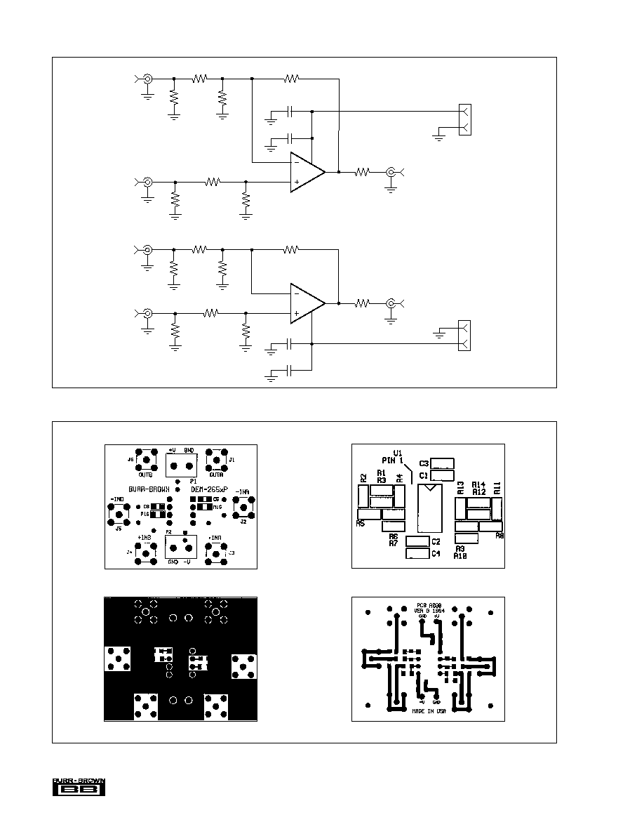
DEMONSTRATION BOARD
PACKAGE
PRODUCT
DEM-OPA265xP
8-Pin DIP
OPA2650P
OPA2650PB
DEM-OPA265xU
SO-8
OPA2650U
OPA2650UB
DEM-OPA26xxE
MSOP-8
OPA2650E
DEMONSTRATION BOARDS
Demonstration boards are available for each OPA2650 pack-
age style. These boards implement a very low parasitic
layout that will produce the excellent frequency and pulse
responses shown in the Typical Performance Curves. For
each package style, the recommended demonstration boards
are:
Contact your local Burr-Brown sales office or distributor to
order demonstration boards.
FIGURE 6. Channel-to-Channel Crosstalk.
TYPICAL APPLICATION
FIGURE 7. Low Distortion Video Amplifier.
OPA2650
V
OUT
402
402
Video
Input
75
75
75
Transmission Line
75
1/2
12
Æ
OPA2650
R
6
R
1
Out
A
J
1
1
2
GND
≠5V
P2
1
2
+5V
GND
P1
R
7
R
5
+In
A
R
3
R
4
R
2
R
15
R
16
≠In
A
J
3
J
2
2
4
1
3
C
2
0.1µF
C
4
2.2µF
R
9
R
14
OPA2650
OPA2650
Out
B
J
6
R
10
R
8
+In
B
R
12
R
13
R
11
≠In
B
J
4
J
5
6
8
7
5
C
3
2.2µF
C
1
0.1µF
1/2
1/2
DEM-OPA265xP Demonstration Board Layout
(A)
(B)
(D)
(C)
FIGURE 9. Evaluation Board Silkscreen (Solder Side). 9b. Evaluation Board Silkscreen (Component Side). 9c. Evaluation
Board Layout (Solder Side). 9d. Evaluation Board (Component Side).
FIGURE 8. Circuit Detail for DEM-OPA265xP Demonstration Board.

PACKAGING INFORMATION
ORDERABLE DEVICE
STATUS(1)
PACKAGE TYPE
PACKAGE DRAWING
PINS
PACKAGE QTY
OPA2650E/250
OBSOLETE
VSSOP
DGK
8
OPA2650E/2K5
OBSOLETE
VSSOP
DGK
8
OPA2650P
OBSOLETE
PDIP
P
8
OPA2650U
OBSOLETE
SOIC
D
8
OPA2650U/2K5
OBSOLETE
SOIC
D
8
OPA2650UB
OBSOLETE
SOIC
D
8
OPA2650UB/2K5
OBSOLETE
SOIC
D
8
(1) The marketing status values are defined as follows:
ACTIVE: Product device recommended for new designs.
LIFEBUY: TI has announced that the device will be discontinued, and a lifetime-buy period is in effect.
NRND: Not recommended for new designs. Device is in production to support existing customers, but TI does not recommend using this part in
a new design.
PREVIEW: Device has been announced but is not in production. Samples may or may not be available.
OBSOLETE: TI has discontinued the production of the device.
PACKAGE OPTION ADDENDUM
www.ti.com
3-Oct-2003

IMPORTANT NOTICE
Texas Instruments Incorporated and its subsidiaries (TI) reserve the right to make corrections, modifications,
enhancements, improvements, and other changes to its products and services at any time and to discontinue
any product or service without notice. Customers should obtain the latest relevant information before placing
orders and should verify that such information is current and complete. All products are sold subject to TI's terms
and conditions of sale supplied at the time of order acknowledgment.
TI warrants performance of its hardware products to the specifications applicable at the time of sale in
accordance with TI's standard warranty. Testing and other quality control techniques are used to the extent TI
deems necessary to support this warranty. Except where mandated by government requirements, testing of all
parameters of each product is not necessarily performed.
TI assumes no liability for applications assistance or customer product design. Customers are responsible for
their products and applications using TI components. To minimize the risks associated with customer products
and applications, customers should provide adequate design and operating safeguards.
TI does not warrant or represent that any license, either express or implied, is granted under any TI patent right,
copyright, mask work right, or other TI intellectual property right relating to any combination, machine, or process
in which TI products or services are used. Information published by TI regarding third-party products or services
does not constitute a license from TI to use such products or services or a warranty or endorsement thereof.
Use of such information may require a license from a third party under the patents or other intellectual property
of the third party, or a license from TI under the patents or other intellectual property of TI.
Reproduction of information in TI data books or data sheets is permissible only if reproduction is without
alteration and is accompanied by all associated warranties, conditions, limitations, and notices. Reproduction
of this information with alteration is an unfair and deceptive business practice. TI is not responsible or liable for
such altered documentation.
Resale of TI products or services with statements different from or beyond the parameters stated by TI for that
product or service voids all express and any implied warranties for the associated TI product or service and
is an unfair and deceptive business practice. TI is not responsible or liable for any such statements.
Following are URLs where you can obtain information on other Texas Instruments products and application
solutions:
Products
Applications
Amplifiers
amplifier.ti.com
Audio
www.ti.com/audio
Data Converters
dataconverter.ti.com
Automotive
www.ti.com/automotive
DSP
dsp.ti.com
Broadband
www.ti.com/broadband
Interface
interface.ti.com
Digital Control
www.ti.com/digitalcontrol
Logic
logic.ti.com
Military
www.ti.com/military
Power Mgmt
power.ti.com
Optical Networking
www.ti.com/opticalnetwork
Microcontrollers
microcontroller.ti.com
Security
www.ti.com/security
Telephony
www.ti.com/telephony
Video & Imaging
www.ti.com/video
Wireless
www.ti.com/wireless
Mailing Address:
Texas Instruments
Post Office Box 655303 Dallas, Texas 75265
Copyright
2003, Texas Instruments Incorporated