Document Outline
- FEATURES
- APPLICATIONS
- DESCRIPTION
- ABSOLUTE MAXIMUM RATINGS
- OPA2684 RELATED PRODUCTS
- PACKAGE/ORDERING INFORMATION
- PIN CONFIGURATION
- ELECTRICAL CHARACTERISTICS: V S =±5V
- ELECTRICAL CHARACTERISTICS: V S =+5V
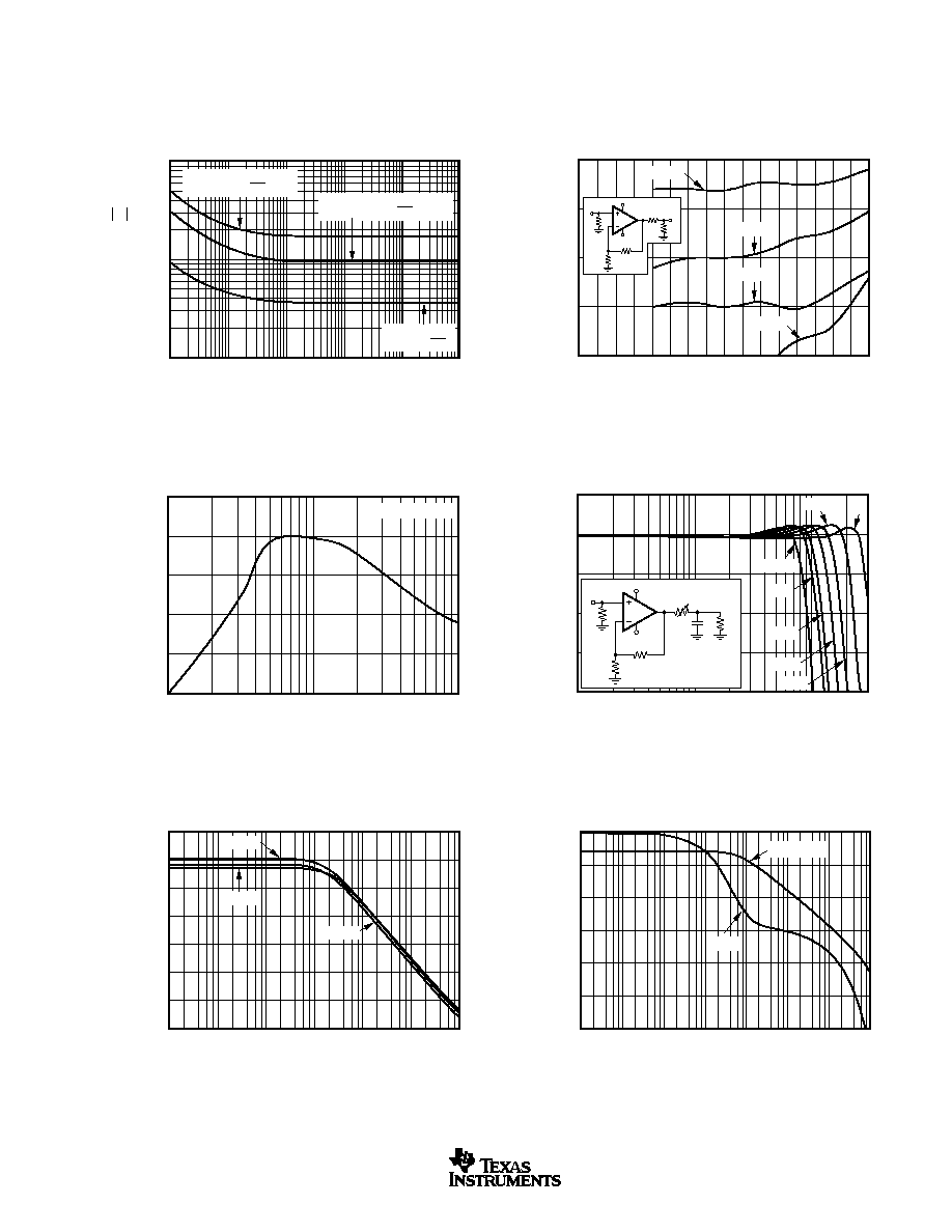
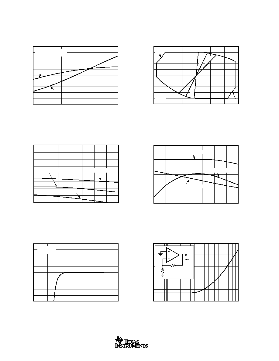
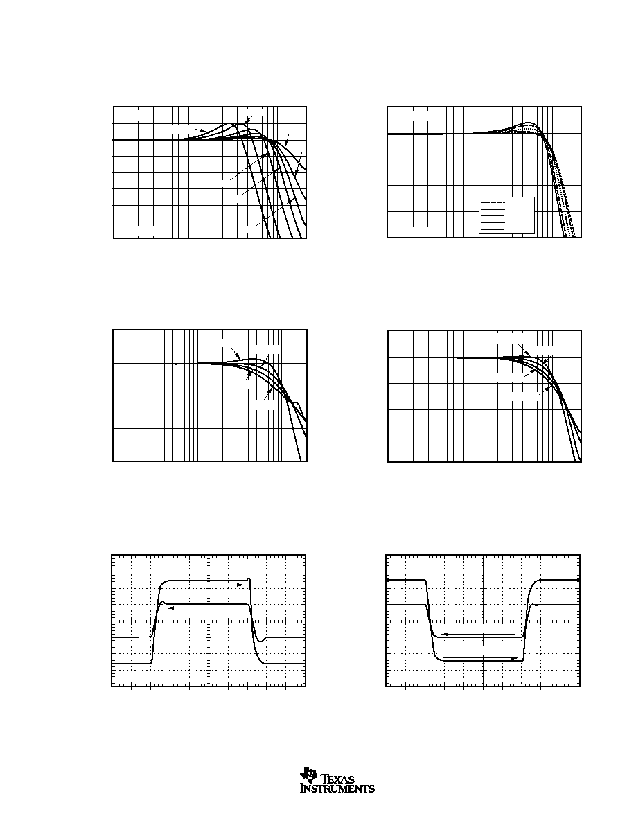
- TYPICAL CHARACTERISTICS: V S =±5V
- TYPICAL CHARACTERISTICS: V S =+5V
- APPLICATIONS INFORMATION
- LOW-POWER, CURRENT-FEEDBACK OPERATION
- DIFFERENTIAL INTERFACE APPLICATIONS
- DC-COUPLED SINGLE TO DIFFERENTIAL CONVERSION
- DIFFERENTIAL ACTIVE FILTER
- SINGLE-SUPPLY, HIGH GAIN DIFFERENTIAL ADC DRIVER
- SYNTHETIC IMPEDANCE DSL LINE DRIVER
- DESIGN-IN TOOLS
- DEMONSTRATION BOARDS
- MACROMODELS
- OPERATING SUGGESTIONS
- SETTING RESISTOR VALUES TO OPTIMIZE BANDWIDTH
- OUTPUT CURRENT AND VOLTAGE
- DRIVING CAPACITIVE LOADS
- DISTORTION PERFORMANCE
- NOISE PERFORMANCE
- DC ACCURACY AND OFFSET CONTROL
- THERMAL ANALYSIS
- BOARD LAYOUT GUIDELINES
- INPUT AND ESD PROTECTION
- PACKAGE DRAWINGS
- D (R-PDSO-G**) PLASTIC SMALL-OUTLINE PACKAGE
- DCN (R-PDSO-G8) PLASTIC SMALL-OUTLINE
OPA2684
www.ti.com
Copyright © 2002, Texas Instruments Incorporated
Please be aware that an important notice concerning availability, standard warranty, and use in critical applications of
Texas Instruments semiconductor products and disclaimers thereto appears at the end of this data sheet.
SBOS239B ≠ APRIL 2002 ≠ REVISED NOVEMBER 2002
Low-Power, Dual Current-Feedback
OPERATIONAL AMPLIFIER
FEATURES
q
MINIMAL BANDWIDTH CHANGE VERSUS GAIN
q
170MHz BANDWIDTH AT G = +2
q
> 120MHz BANDWIDTH TO GAIN > +10
q
LOW DISTORTION: < ≠82dBc at 5MHz
q
HIGH OUTPUT CURRENT: 120mA
q
SINGLE +5V TO +12V SUPPLY OPERATION
q
DUAL
±
2.5 TO
±
6.0V SUPPLY OPERATION
q
LOW SUPPLY CURRENT: 3.4mA Total
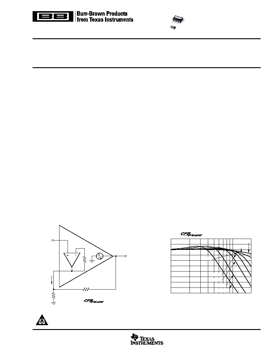
V+
V
O
V≠
I
ERR
R
G
R
F
Z
(S)
I
ERR
+
Low-Power
Amplifier
1 of 2 Channels
DESCRIPTION
The OPA2684 provides a new level of performance in low-
power, wideband, current-feedback (CFB) amplifiers. This
CFB
PLUS
amplifier is among the first to use an internally
closed-loop input buffer stage that enhances performance
significantly over earlier low-power CFB amplifiers. While
retaining the benefits of very low power operation, this new
architecture provides many of the benefits of a more ideal
CFB amplifier. The closed-loop input stage buffer gives a
very low and linearized impedance path at the inverting input
to sense the feedback error current. This improved inverting
input impedance retains exceptional bandwidth to much
higher gains and improves harmonic distortion over earlier
solutions limited by inverting input linearity. Beyond simple
high-gain applications, the OPA2684 CFB
PLUS
amplifier per-
mits the gain setting element to be set with considerable
APPLICATIONS
q
SHORT-LOOP ADSL CO DRIVER
q
LOW-POWER BROADCAST VIDEO DRIVERS
q
DIFFERENTIAL EQUALIZING FILTERS
q
DIFFERENTIAL SAW FILTER POST AMPLIFIER
q
MULTICHANNEL SUMMING AMPLIFIERS
q
PROFESSIONAL CAMERAS
q
ADC INPUT DRIVERS
freedom from amplifier bandwidth interaction. This allows
frequency response peaking elements to be added, multiple
input inverting summing circuits to have greater bandwidth,
and low-power line drivers to meet the demanding require-
ments of studio cameras and broadcast video.
The output capability of the OPA2684 also sets a new mark
in performance for low-power, current-feedback amplifiers.
Delivering a full
±
4Vp-p swing on
±
5V supplies, the OPA2684
also has the output current to support >
±
3Vp-p into 50
loads. This minimal output headroom requirement is comple-
mented by a similar 1.2V input stage headroom giving
exceptional capability for single +5V operation.
The OPA2684's low 3.4mA supply current is precisely trimmed
at +25
∞
C. This trim, along with low shift over temperature and
supply voltage, gives a very robust design over a wide range
of operating conditions.
6
3
0
≠3
≠6
≠9
≠12
≠15
≠18
≠21
≠24
Normalized Gain (3dB/div)
R
F
= 800
G = 100
G = 50
G = 20
G = 10
G = 2
G = 1
10
MHz
100
200
BW (MHz) vs GAIN
G = 5
Patent Pending
OPA2
684
PRODUCTION DATA information is current as of publication date.
Products conform to specifications per the terms of Texas Instruments
standard warranty. Production processing does not necessarily include
testing of all parameters.

OPA2684
2
SBOS239B
www.ti.com
SPECIFIED
PACKAGE
TEMPERATURE
PACKAGE
ORDERING
TRANSPORT
PRODUCT
PACKAGE-LEAD
DESIGNATOR
(1)
RANGE
MARKING
NUMBER
MEDIA, QUANTITY
OPA2684
SO-8
D
≠40
∞
C to +85
∞
C
OPA2684
OPA2684ID
Rails, 100
"
"
"
"
"
OPA2684IDR
Tape and Reel, 2500
OPA2684
SOT23-8
DCN
≠40
∞
C to +85
∞
C
A84
OPA2684IDCNT
Tape and Reel, 250
"
"
"
"
"
OPA2684IDCNR
Tape and Reel, 3000
ABSOLUTE MAXIMUM RATINGS
(1)
Power Supply ...............................................................................
±
6.5V
DC
Internal Power Dissipation ................................. See Thermal Information
Differential Input Voltage ..................................................................
±
1.2V
Input Voltage Range ............................................................................
±
V
S
Storage Temperature Range: ID, IDBV ......................... ≠40
∞
C to +125
∞
C
Lead Temperature (soldering, 10s) .............................................. +300
∞
C
Junction Temperature (T
J
) ........................................................... +175
∞
C
ESD Rating: Human Body Model (HBM) ........................................ 2000V
Charged Device Model (CDM) .................................. 1500V
NOTE: (1) Stresses above these ratings may cause permanent damage.
Exposure to absolute maximum conditions for extended periods may degrade
device reliability.
PACKAGE/ORDERING INFORMATION
ELECTROSTATIC
DISCHARGE SENSITIVITY
This integrated circuit can be damaged by ESD. Texas Instru-
ments recommends that all integrated circuits be handled with
appropriate precautions. Failure to observe proper handling
and installation procedures can cause damage.
ESD damage can range from subtle performance degradation to
complete device failure. Precision integrated circuits may be more
susceptible to damage because very small parametric changes
could cause the device not to meet its published specifications.
PIN CONFIGURATION
OPA2684 RELATED PRODUCTS
SINGLES
DUALS
TRIPLES
QUADS
FEATURES
OPA684
OPA2683
OPA3684
OPA2684
Low-Power CFB
PLUS
OPA691
OPA2691
OPA3691
--
High Slew Rate CFB
OPA685
--
--
--
> 500MHz CFB
Top View
SO
Top View
SOT
NOTE: (1) For the most current specifications, and package information, refer to our web site at www.ti.com.
1
2
3
4
8
7
6
5
+V
S
Out B
≠In B
+In B
Out A
≠In A
+In A
≠V
S
OPA2684
1
2
3
4
8
7
6
5
Out A
≠In A
+In A
≠V
S
+V
S
Out B
≠In B
+In B
A84
Pin 1
OPA2684
3
SBOS239B
www.ti.com
AC PERFORMANCE (see Figure 1)
Small-Signal Bandwidth (V
O
= 0.5Vp-p)
G = +1, R
F
= 800
250
MHz
typ
C
G = +2, R
F
= 800
170
120
118
117
MHz
min
B
G = +5, R
F
= 800
138
MHz
typ
C
G = +10, R
F
= 800
120
MHz
typ
C
G = +20, R
F
= 800
95
MHz
typ
C
Bandwidth for 0.1dB Gain Flatness
G = +2, V
O
= 0.5Vp-p, R
F
= 800
19
16
14
14
MHz
min
B
Peaking at a Gain of +1
R
F
= 800
, V
O
= 0.5Vp-p
1.4
4.8
5.9
6.3
dB
max
B
Large-Signal Bandwidth
G = +2, V
O
= 4Vp-p
90
MHz
typ
C
Slew Rate
G = ≠1, V
O
= 4V Step
780
675
650
575
V/
µ
s
min
B
G = +2, V
O
= 4V Step
750
680
660
656
V/
µ
s
min
B
Rise-and-Fall Time
G = +2, V
O
= 0.5V Step
3
ns
typ
C
G = +2, V
O
= 4V Step
3.8
ns
typ
C
Harmonic Distortion
G = +2, f = 5MHz, V
O
= 2Vp-p
2nd-Harmonic
R
L
= 100
≠67
≠59
≠59
≠58
dBc
max
B
R
L
1k
≠82
≠66
≠65
≠65
dBc
max
B
3rd-Harmonic
R
L
= 100
≠70
≠66
≠65
≠65
dBc
max
B
R
L
1k
≠84
≠82
≠81
≠81
dBc
max
B
Input Voltage Noise
f > 1MHz
3.7
4.1
4.2
4.4
nV/
Hz
max
B
Noninverting Input Current Noise
f > 1MHz
9.4
11
12
12.5
pA/
Hz
max
B
Inverting Input Current Noise
f > 1MHz
17
18
18.5
19
pA/
Hz
max
B
Differential Gain
G = +2, NTSC, V
O
= 1.4Vp, R
L
= 150
0.04
%
typ
C
Differential Phase
G = +2, NTSC, V
O
= 1.4Vp, R
L
= 150
0.02
deg
typ
C
Channel-to-Channel Isolation
f = 5MHz
70
dB
typ
C
DC PERFORMANCE
(4)
Open-Loop Transimpedance Gain (Z
OL
)
V
O
= 0V, R
L
= 1k
355
160
155
153
k
min
A
Input Offset Voltage
V
CM
= 0V
±
1.5
±
3.8
±
4.4
±
4.6
mV
max
A
Average Offset Voltage Drift
V
CM
= 0V
±
12
±
12
µ
V/
∞
C
max
B
Noninverting Input Bias Current
V
CM
= 0V
±
5.0
±
11
±
12.5
±
13
µ
A
max
A
Average Noninverting Input Bias Current Drift
V
CM
= 0V
±
25
±
30
nA/
∞
C
max
B
Inverting Input Bias Current
V
CM
= 0V
±
5.0
±
17
±
18.5
±
19.5
µ
A
max
A
Average Inverting Input Bias Current Drift
V
CM
= 0V
±
35
±
40
nA
∞
/C
max
B
INPUT
Common-Mode Input Range
(5)
(CMIR)
±
3.75
±
3.65
±
3.65
±
3.6
V
min
A
Common-Mode Rejection Ratio (CMRR)
V
CM
= 0V
60
53
52
52
dB
min
A
Noninverting Input Impedance
50 || 2
k
|| pF
typ
C
Inverting Input Resistance (R
I
)
Open-Loop, DC
4.0
typ
C
OUTPUT
Voltage Output Swing
1k
Load
±
4.1
±
3.9
±
3.9
±
3.8
V
min
A
Current Output, Sourcing
V
O
= 0
160
130
125
120
mA
min
A
Current Output, Sinking
V
O
= 0
≠120
≠100
≠95
≠90
mA
min
A
Closed-Loop Output Impedance
G = +2, f = 100kHz
0.006
typ
C
POWER SUPPLY
Specified Operating Voltage
±
5
V
typ
C
Maximum Operating Voltage Range
±
6
±
6
±
6
V
max
A
Max Quiescent Current
V
S
=
±
5V
3.4
3.6
3.9
3.9
mA
max
A
Min Quiescent Current
V
S
=
±
5V
3.4
3.2
3.1
2.9
mA
min
A
Power-Supply Rejection Ratio (≠PSRR)
Input Referred
60
54
53
53
dB
typ
A
TEMPERATURE RANGE
Specification: ID, IDCN
≠40 to +85
∞
C
typ
C
Thermal Resistance,
JA
Junction-to-Ambient
D
SO-8
125
∞
C/W
typ
C
DCN SOT23-8
150
∞
C/W
typ
C
NOTES: (1) Junction temperature = ambient for +25
∞
C tested specifications. (2) Junction temperature = ambient at low temperature limit, junction temperature = ambient
+2
∞
C at high temperature limit for over temperature tested specifications. (3) Test levels: (A) 100% tested at +25
∞
C. Over temperature limits by characterization and
simulation. (B) Limits set by characterization and simulation. (C) Typical value only for information. (4) Current is considered positive out-of-node. V
CM
is the input
common-mode voltage. (5) Tested < 3dB below minimum specified CMR at
±
CMIR limits.
OPA2684ID, IDCN
0
∞
C to
≠40
∞
C to
MIN/
TEST
PARAMETER
CONDITIONS
+25
∞
C
+25
∞
C
(1)
70
∞
C
(2)
+85
∞
C
(2)
UNITS
MAX
LEVEL
(3)
TYP
MIN/MAX OVER TEMPERATURE
ELECTRICAL CHARACTERISTICS: V
S
=
±
5V
Boldface limits are tested at +25
∞
C.
R
F
= 800
, R
L
= 100
, and G = +2
,
(see Figure 1 for AC performance only), unless otherwise noted.
OPA2684
4
SBOS239B
www.ti.com
AC PERFORMANCE (see Figure 3)
Small-Signal Bandwidth (V
O
= 0.5Vp-p)
G = +1, R
F
= 1.0k
140
MHz
typ
C
G = +2, R
F
= 1.0k
110
86
85
82
MHz
min
B
G = +5, R
F
= 1.0k
100
MHz
min
C
G = +10, R
F
= 1.0k
90
MHz
typ
C
G = +20, R
F
= 1.0k
75
MHz
typ
C
Bandwidth for 0.1dB Gain Flatness
G = +2, V
O
< 0.5Vp-p, R
F
= 1.0k
21
12
11
10
MHz
min
B
Peaking at a Gain of +1
R
F
= 1.0k
, V
O
< 0.5Vp-p
0.5
2.6
3.4
3.7
dB
max
B
Large-Signal Bandwidth
G = 2, V
O
= 2Vp-p
86
MHz
typ
C
Slew Rate
G = 2, V
O
= 2V Step
380
300
290
280
V/
µ
s
min
B
Rise-and-Fall Time
G = 2, V
O
= 0.5V Step
4.3
ns
typ
C
G = 2, V
O
= 2VStep
4.8
ns
typ
C
Harmonic Distortion
G = 2, f = 5MHz, V
O
= 2Vp-p
2nd-Harmonic
R
L
= 100
to V
S
/2
≠65
≠60
≠59
≠59
dBc
max
B
R
L
1k
to V
S
/2
≠84
≠62
≠61
≠61
dBc
max
B
3rd-Harmonic
R
L
= 100
to V
S
/2
≠65
≠64
≠63
≠63
dBc
max
B
R
L
1k
to V
S
/2
≠74
≠70
≠70
≠69
dBc
max
B
Input Voltage Noise
f > 1MHz
3.7
4.1
4.2
4.4
nV/
Hz
max
B
Noninverting Input Current Noise
f > 1MHz
9.4
11
12
12.5
pA/
Hz
max
B
Inverting Input Current Noise
f > 1MHz
17
18
18.5
19
pA/
Hz
max
B
Differential Gain
G = +2, NTSC, V
O
= 1.4Vp, R
L
= 150
0.04
%
typ
C
Differential Phase
G = +2, NTSC, V
O
= 1.4Vp, R
L
= 150
0.07
deg
typ
C
Channel-to-Channel Isolation
f = 5MHz
70
dB
typ
C
DC PERFORMANCE
(4)
Open-Loop Transimpedance Gain (Z
OL
)
V
O
= V
S
/2, R
L
= 1k
to V
S
/2
355
160
155
153
k
min
A
Input Offset Voltage
V
CM
= V
S
/2
±
1.0
±
3.3
±
3.9
±
4.1
mV
max
A
Average Offset Voltage Drift
V
CM
= V
S
/2
±
12
±
12
µ
V/
∞
C
max
B
Noninverting Input Bias Current
V
CM
= V
S
/2
±
5
±
11
±
12.5
±
13
µ
A
max
A
Average Noninverting Input Bias Current Drift
V
CM
= V
S
/2
±
25
±
30
nA/
∞
C
max
B
Inverting Input Bias Current
V
CM
= V
S
/2
±
5
±
13
±
14.5
±
16
µ
A
max
A
Average Inverting Input Bias Current Drift
V
CM
= V
S
/2
±
25
±
30
nA
∞
/C
max
B
INPUT
Least Positive Input Voltage
(5)
1.25
1.32
1.35
1.38
V
max
A
Most Positive Input Voltage
(5)
3.75
3.68
3.65
3.62
V
min
A
Common-Mode Refection Ratio (CMRR)
V
CM
= V
S
/2
58
52
51
51
dB
min
A
Noninverting Input Impedance
50 || 1
k
|| pF
typ
C
Inverting Input Resistance (R
I
)
Open-Loop
4.4
typ
C
OUTPUT
Most Positive Output Voltage
R
L
= 1k
to V
S
/2
4.10
3.9
3.9
3.8
V
min
A
Least Positive Output Voltage
R
L
= 1k
to V
S
/2
0.9
1.1
1.1
1.2
V
max
A
Current Output, Sourcing
V
O
= V
S
/2
80
65
60
55
mA
min
A
Current Output, Sinking
V
O
= V
S
/2
70
55
50
45
mA
min
A
Closed-Loop Output Impedance
G = +2, f = 100kHz
0.006
typ
C
POWER SUPPLY
Specified Single-Supply Operating Voltage
5
V
typ
C
Max Single-Supply Operating Voltage Range
12
12
12
V
max
A
Max Quiescent Current
V
S
= +5V
2.9
3.1
3.1
3.1
mA
max
A
Min Quiescent Current
V
S
= +5V
2.9
2.6
2.4
2.3
mA
min
A
Power-Supply Rejection Ratio (+PSRR)
Input Referred
58
dB
typ
C
TEMPERATURE RANGE
Specification: ID, IDBV
≠40 to +85
∞
C
typ
C
Thermal Resistance,
JA
Junction-to-Ambient
D
SO-8
125
∞
C/W
typ
C
DCN SOT23-8
150
∞
C/W
typ
C
NOTES: (1) Junction temperature = ambient for +25
∞
C tested specifications. (2) Junction temperature = ambient at low temperature limit, junction temperature = ambient
+1
∞
C at high temperature limit for over temperature tested specifications. (3) Test levels: (A) 100% tested at +25
∞
C. Over temperature limits by characterization and
simulation. (B) Limits set by characterization and simulation. (C) Typical value only for information. (4) Current is considered positive out-of-node. V
CM
is the input
common-mode voltage. (5) Tested < 3dB below minimum specified CMR at
±
CMIR limits.
ELECTRICAL CHARACTERISTICS: V
S
= +5V
Boldface limits are tested at +25
∞
C.
R
F
= 1k
, R
L
= 100
, and G = +2
,
(see Figure 3 for AC performance only), unless otherwise noted.
OPA2684ID, IDCN
0
∞
C to
≠40
∞
C to
MIN/
TEST
PARAMETER
CONDITIONS
+25
∞
C
+25
∞
C
(1)
70
∞
C
(2)
+85
∞
C
(2)
UNITS
MAX
LEVEL
(3)
TYP
MIN/MAX OVER TEMPERATURE

OPA2684
5
SBOS239B
www.ti.com
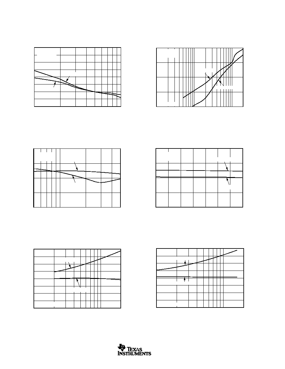
TYPICAL CHARACTERISTICS: V
S
=
±
5V
At T
A
= +25
∞
C, G = +2, R
F
= 800
, and R
L
= 100
, unless otherwise noted.
6
3
0
≠3
≠6
≠9
≠12
≠15
≠18
Frequency (MHz)
1
200
10
100
NONINVERTING SMALL-SIGNAL
FREQUENCY RESPONSE
Normalized Gain (3dB/div)
V
O
= 0.5Vp-p
R
F
= 800
See Figure 1
G = 1
G = 2
G = 50
G = 20
G = 10
G = 5
G = 100
3
0
≠3
≠6
≠9
≠12
Frequency (MHz)
1
200
10
100
INVERTING SMALL-SIGNAL FREQUENCY RESPONSE
Normalized Gain (3dB/div)
V
O
= 0.5Vp-p
R
F
= 800
See Figure 2
G = ≠1
G = ≠10
G = ≠16
G = ≠5
G = ≠2
9
6
3
0
≠3
Frequency (MHz)
1
200
10
100
NONINVERTING LARGE-SIGNAL
FREQUENCY RESPONSE
Gain (dB)
G = +2
R
L
= 100
See Figure 1
V
O
= 1Vp-p
V
O
= 0.5Vp-p
V
O
= 5Vp-p
V
O
= 2Vp-p
3
0
≠3
≠6
≠9
≠12
Frequency (MHz)
1
200
10
100
INVERTING LARGE-SIGNAL FREQUENCY RESPONSE
Gain (dB)
G = ≠1
R
L
= 100
V
O
= 0.5Vp-p
See Figure 2
2Vp-p
1Vp-p
5Vp-p
NONINVERTING PULSE RESPONSE
Time (10ns/div)
Output V
oltage (200mV/div)
Output V
oltage (400mV/div)
0.8
0.6
0.4
0.2
0
≠0.2
≠0.4
≠0.6
≠0.8
1.6
1.2
0.8
0.4
0
≠0.4
≠0.8
≠1.2
≠1.6
Large-Signal Right Scale
Small-Signal Left Scale
See Figure 1
G = +2
INVERTING PULSE RESPONSE
Time (10ns/div)
Output V
oltage (200mV/div)
Output V
oltage (400mV/div)
0.8
0.6
0.4
0.2
0
≠0.2
≠0.4
≠0.6
≠0.8
1.6
1.2
0.8
0.4
0
≠0.4
≠0.8
≠1.2
≠1.6
Large-Signal Right Scale
Small-Signal Left Scale
See Figure 2
G = ≠1
OPA2684
6
SBOS239B
www.ti.com
TYPICAL CHARACTERISTICS: V
S
=
±
5V
(Cont.)
At T
A
= +25
∞
C, G = +2, R
F
= 800
, and R
L
= 100
, unless otherwise noted.
HARMONIC DISTORTION vs LOAD RESISTANCE
100
1k
Load Resistance (
)
Harmonic Distortion (dBc)
≠50
≠55
≠60
≠65
≠70
≠75
≠80
≠85
≠90
V
O
= 2Vp-p
f = 5MHz
G = +2
See Figure 1
2nd-Harmonic
3rd-Harmonic
≠50
≠60
≠70
≠80
≠90
Frequency (MHz)
0.1
20
1
10
HARMONIC DISTORTION vs FREQUENCY
Harmonic Distortion (dBc)
V
O
= 2Vp-p
R
L
= 100
See Figure 1
2nd-Harmonic
3rd-Harmonic
HARMONIC DISTORTION vs OUTPUT VOLTAGE
0.5
1
5
Output Voltage (Vp-p)
Harmonic Distortion (dBc)
≠50
≠60
≠70
≠80
≠90
f = 5MHz
R
L
= 100
2nd-Harmonic
3rd-Harmonic
5MHz HARMONIC DISTORTION vs SUPPLY VOLTAGE
±
2.5
±
3
±
3.5
±
4
±
4.5
±
5
±
5.5
±
6
Supply Voltage (
±
V)
Harmonic Distortion (dBc)
≠50
≠60
≠70
≠80
≠90
V
O
= 2Vp-p
R
L
= 100
2nd-Harmonic
3rd-Harmonic
HARMONIC DISTORTION vs NONINVERTING GAIN
Noninverting Gain (V/V)
Harmonic Distortion (dBc)
1
10
20
≠50
≠55
≠60
≠65
≠70
≠75
≠80
≠85
≠90
2nd-Harmonic
3rd-Harmonic
See Figure 1
HARMONIC DISTORTION vs INVERTING GAIN
1
10
20
Inverting Gain
(V/V)
Harmonic Distortion (dBc)
≠50
≠55
≠60
≠65
≠70
≠75
≠80
≠85
≠90
2nd-Harmonic
3rd-Harmonic
See Figure 2
OPA2684
7
SBOS239B
www.ti.com
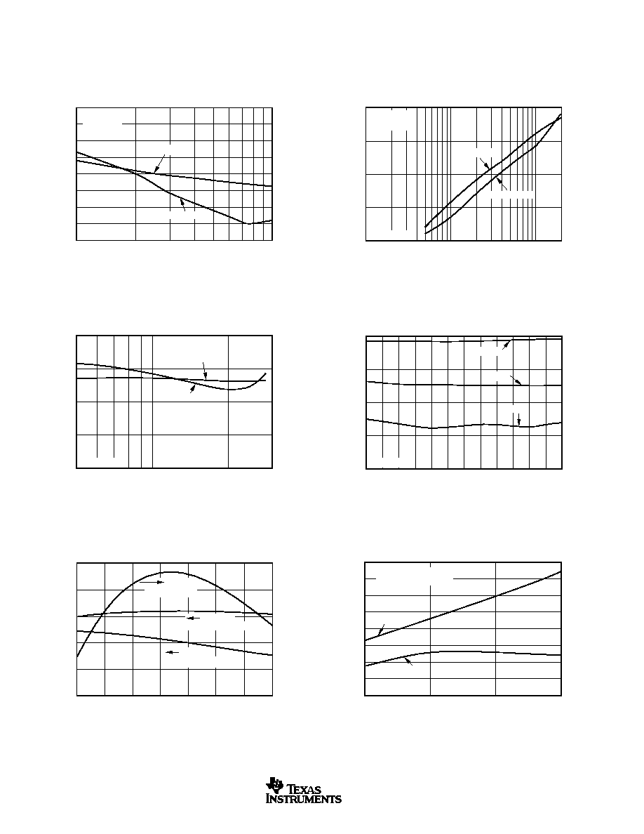
TYPICAL CHARACTERISTICS: V
S
=
±
5V
(Cont.)
At T
A
= +25
∞
C, G = +2, R
F
= 800
, and R
L
= 100
, unless otherwise noted.
100
10
1
Frequency (Hz)
100
10M
1k
10k
100k
1M
INPUT VOLTAGE AND CURRENT NOISE DENSITY
Voltage Noise (nV/
Hz)
Current Noise (pA/
Hz)
Noninverting Current Noise
9.4pA/
Hz
Voltage Noise
3.7nV/
Hz
Inverting Current Noise
17pA/
Hz
2-TONE, 3RD-ORDER
INTERMODULATION DISTORTION
≠8 ≠7 ≠6 ≠5 ≠4 ≠3 ≠2 ≠1
4
5
3
2
1
0
6
7
8
Power at Load (P
O
each tone, dBm)
3rd-Order Spurious Level (dBc)
≠50
≠60
≠70
≠80
≠90
50
+5V
≠5V
50
50
P
I
P
O
800
800
OPA2684
20MHz
10MHz
5MHz
1MHz
50
40
30
20
10
0
C
LOAD
(pF)
1
100
10
R
S
vs C
LOAD
R
S
(
)
0.5dB Peaking
9
6
3
0
≠3
≠6
Frequency (MHz)
1
300
10
100
SMALL-SIGNAL BANDWIDTH vs C
LOAD
Normalized Gain (dB)
5pF
800
1k
OPA2684
R
S
V
O
+5V
≠5V
50
C
L
800
V
I
12pF
100pF
50pF
75pF
20pF
33pF
1k
is
Optional
CMRR and PSRR vs FREQUENCY
10
2
10
3
10
4
10
5
10
6
10
7
10
8
Frequency (Hz)
Power-Supply Rejection Ratio (dB)
Common-Mode Rejection Ratio (dB)
70
60
50
40
30
20
10
0
CMRR
+PSRR
≠PSRR
OPEN-LOOP TRANSIMPEDANCE GAIN AND PHASE
10
2
10
3
10
4
10
5
10
6
10
7
10
8
10
9
Frequency (Hz)
Open-Loop
T
ransimpedance Gain (dB
) 120
100
80
60
40
20
0
Open-Loop Phase (
∞
)
0
≠30
≠60
≠90
≠120
≠150
≠180
20log (Z
OL
)
Z
OL
OPA2684
8
SBOS239B
www.ti.com
TYPICAL CHARACTERISTICS: V
S
=
±
5V
(Cont.)
At T
A
= +25
∞
C, G = +2, R
F
= 800
, and R
L
= 100
, unless otherwise noted.
0.10
0.09
0.08
0.07
0.06
0.05
0.04
0.03
0.02
0.01
0
Number of 150
Video Loads
1
4
2
3
COMPOSITE VIDEO DIFFERENTIAL GAIN/PHASE
Differential Gain (%)
Differential Phase (
∞
)
Gain = +2
NTSC, Positive Video
dG
dP
OUTPUT CURRENT AND VOLTAGE LIMITATIONS
≠150
≠100
≠50
0
50
100
150
I
O
(mA)
V
O
(V)
5
4
3
2
1
0
≠1
≠2
≠3
≠4
≠5
1W Power
Limit
Each
Channel
R
L
= 100
R
L
=
5
0
R
L
= 500
1W Power
Limit
TYPICAL DC DRIFT OVER AMBIENT TEMPERATURE
≠50
≠25
0
25
50
75
100
125
Ambient Temperature (
∞
C)
Input Bias Currents (
µ
A)
and Of
fset V
oltage (mV)
4
3
2
1
0
≠1
≠2
≠3
≠4
Input Offset Voltage
Noninverting Input Bias Current
Inverting Input Bias Current
SUPPLY AND OUTPUT CURRENT
vs AMBIENT TEMPERATURE
≠50
≠25
25
0
50
75
100
125
Ambient Temperature (
∞
C)
Output Current (mA)
200
175
150
125
100
Supply Current (mA)
Sourcing Output Current
Sinking Output Current
Supply Current
3.8
3.6
3.4
3.2
3
SETTLING TIME
0
10
20
30
40
50
60
Time (ns)
Error to Final V
alue (%)
0.05
0.04
0.03
0.02
0.01
0
≠0.01
≠0.02
≠0.03
≠0.04
≠0.05
2V Step
See Figure 1
CLOSED-LOOP OUTPUT IMPEDANCE vs FREQUENCY
Frequency (Hz)
100k
1M
1k
10k
100
10M
100M
Output Impedance (
)
100
10
1
0.01
0.001
800
Z
O
800
1/2
OPA2684
OPA2684
9
SBOS239B
www.ti.com
TYPICAL CHARACTERISTICS: V
S
=
±
5V
(Cont.)
At T
A
= +25
∞
C, G = +2, R
F
= 800
, and R
L
= 100
, unless otherwise noted.
NONINVERTING OVERDRIVE RECOVERY
Time (100ns/div)
Input V
oltage (0.8V/div)
Output V
oltage (1.6V/div)
4.0
3.2
2.4
1.6
0.8
0
≠0.8
≠1.6
≠2.4
≠3.2
≠4.0
8.0
6.4
4.8
3.2
1.6
0
≠1.6
≠3.2
≠4.8
≠6.4
≠8.0
See Figure 1
Input Voltage
Left-Scale
Output Voltage
Right-Scale
INVERTING OVERDRIVE RECOVERY
Time (100ns/div)
Input V
oltage (1.6V/div)
Output V
oltage (1.6V/div)
8.0
6.4
4.8
3.2
1.6
0
≠1.6
≠3.2
≠4.8
≠6.4
≠8.0
8.0
6.4
4.8
3.2
1.6
0
≠1.6
≠3.2
≠4.8
≠6.4
≠8.0
See Figure 2
Input Voltage
Left-Scale
Output Voltage
Right-Scale
INPUT AND OUTPUT RANGE vs SUPPLY VOLTAGE
±
Supply Voltage (V)
±
4
±
3
±
2
±
5
±
6
Input and Output V
oltage Range (V)
6
5
4
3
2
1
0
≠1
≠2
≠3
≠4
≠5
≠6
Input
Voltage
Range
Output
Voltage
Range
OPA2684
10
SBOS239B
www.ti.com
≠55
≠60
≠65
≠70
≠75
≠80
≠85
Load Resistance (
)
10
1k
100
DIFFERENTIAL DISTORTION
vs LOAD RESISTANCE
Harmonic Distortion (dBc)
V
O
= 4Vp-p
G
D
= 2
f = 5MHz
3rd-Harmonic
2nd-Harmonic
≠55
≠60
≠65
≠70
≠75
≠80
≠85
DIFFERENTIAL DISTORTION vs FREQUENCY
Frequency (MHz)
1
10
Harmonic Distortion (dBc)
3rd-Harmonic
2nd-Harmonic
V
O
= 4Vp-p
G
D
= 2
R
L
= 100
≠55
≠60
≠65
≠70
≠75
≠80
≠85
DIFFERENTIAL DISTORTION
vs OUTPUT VOLTAGE
Output Voltage (Vp-p)
1
10
Harmonic Distortion (dBc)
3rd-Harmonic
2nd-Harmonic
f = 5MHz
G
D
= 2
R
L
= 100
1/2
OPA2684
R
G
800
+5V
1/2
OPA2684
R
G
R
L
V
I
800
V
O
≠5V
G
D =
804
R
G
6
3
0
≠3
≠6
≠9
≠12
≠15
≠18
≠21
≠24
Frequency (MHz)
1
200
10
100
DIFFERENTIAL SMALL-SIGNAL
FREQUENCY RESPONSE
Normalized Gain (dB)
V
O
= 200mVp-p
G = 2
G = 20
G = 10
G = 5
G = 1
9
6
3
0
≠3
≠6
≠9
≠12
≠15
≠18
Frequency (Hz)
1
200
10
100
DIFFERENTIAL LARGE-SIGNAL
FREQUENCY RESPONSE
Normalized Gain (dB)
G
D
= 2
R
L
= 100
V
O
= 0.2Vp-p
V
O
= 1Vp-p
V
O
= 2Vp-p
V
O
= 5Vp-p
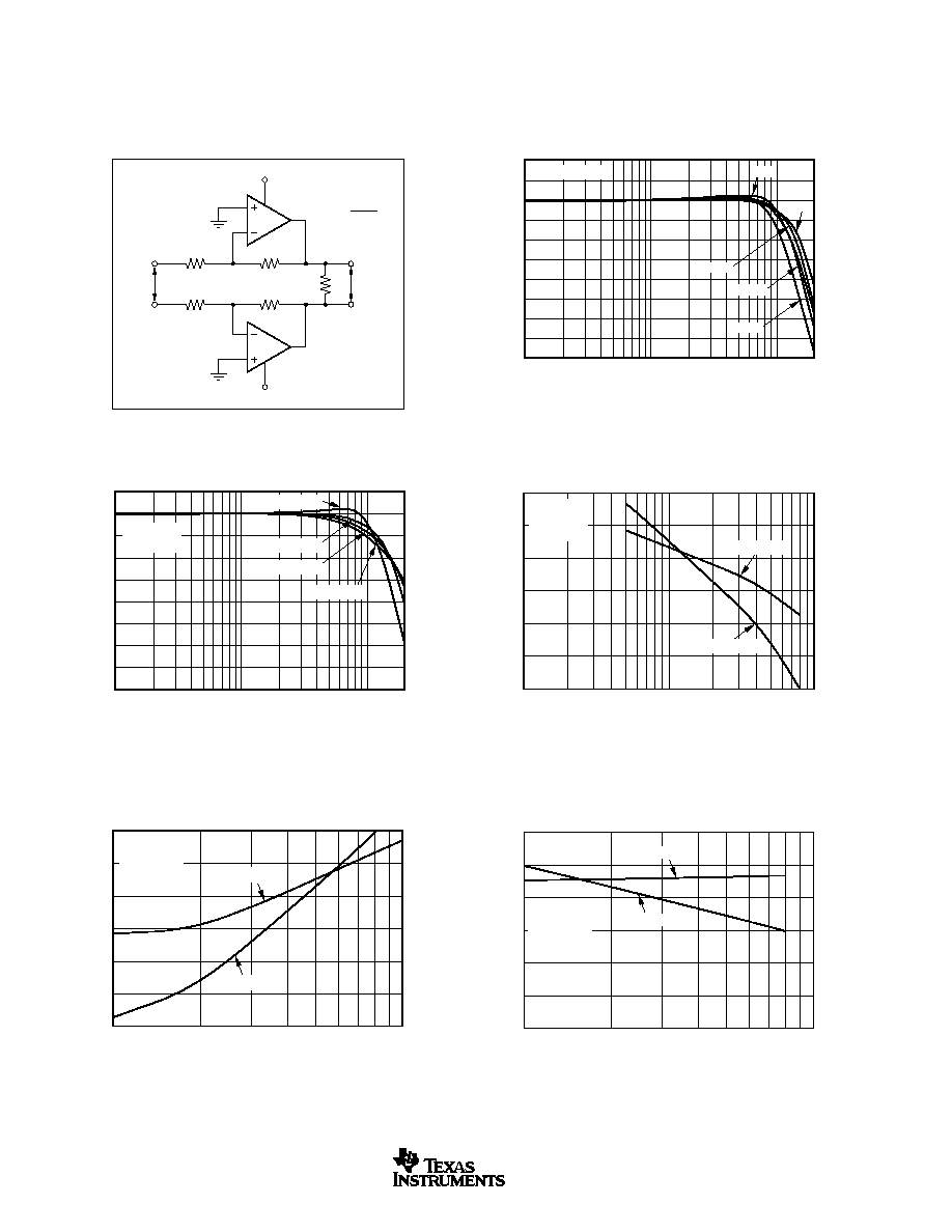
DIFFERENTIAL PERFORMANCE
TEST CIRCUIT
TYPICAL CHARACTERISTICS: V
S
=
±
5V
(Cont.)
At T
A
= +25
∞
C, G = +2, R
F
= 800
, R
L
= 100
, unless otherwise noted.
OPA2684
11
SBOS239B
www.ti.com
6
3
0
≠3
≠6
≠9
≠12
≠15
≠18
Frequency (MHz)
1
200
10
100
NONINVERTING SMALL-SIGNAL
FREQUENCY RESPONSE
Normalized Gain (3dB/div)
G = 100
See Figure 3
G = 50
R
F
= 1k
G = 1
G = 2
G = 5
G = 20
G = 10
3
0
≠3
≠6
≠9
≠12
Frequency (MHz)
1
200
10
100
INVERTING SMALL-SIGNAL FREQUENCY RESPONSE
Normalized Gain (3dB/div)
See Figure 4
R
F
= 1.0k
G = ≠1
G = ≠10
G = ≠20
G = ≠5
G = ≠2
9
6
3
0
≠3
Frequency (MHz)
1
200
10
100
NONINVERTING LARGE-SIGNAL
FREQUENCY RESPONSE
Gain (dB)
0.2Vp-p
1Vp-p
0.5Vp-p
2Vp-p
TYPICAL CHARACTERISTICS: V
S
= +5V
At T
A
= +25
∞
C, V
S
= 5V, G = +2, R
F
= 1.0k
, and R
L
= 100
, unless otherwise noted.
3
0
≠3
≠6
≠9
≠12
Frequency (MHz)
1
200
10
100
INVERTING LARGE-SIGNAL FREQUENCY RESPONSE
Gain (dB)
V
O
= 0.2Vp-p
V
O
= 1Vp-p
V
O
= 0.5Vp-p
V
O
= 2Vp-p
NONINVERTING PULSE RESPONSE
Time (10ns/div)
Output V
oltage (200mV/div)
Output V
oltage (400mV/div)
0.4
0.3
0.2
0.1
0
≠0.1
≠0.2
≠0.3
≠0.4
1.6
1.2
0.8
0.4
0
≠0.4
≠0.8
≠1.2
≠1.6
Large-Signal Right Scale
Small-Signal Left Scale
See Figure 3
INVERTING PULSE RESPONSE
Time (10ns/div)
Output V
oltage (200mV/div)
Output V
oltage (400mV/div)
0.4
0.3
0.2
0.1
0
≠0.1
≠0.2
≠0.3
≠0.4
1.6
1.2
0.8
0.4
0
≠0.4
≠0.8
≠1.2
≠1.6
Large-Signal Right Scale
Small-Signal Left Scale
See Figure 4
OPA2684
12
SBOS239B
www.ti.com
TYPICAL CHARACTERISTICS: V
S
= +5V
(Cont.)
At T
A
= +25
∞
C, V
S
= 5V, G = +2, R
F
= 1.0k
, and R
L
= 100
, unless otherwise noted.
HARMONIC DISTORTION vs LOAD RESISTANCE
100
1k
Load Resistance (
)
Harmonic Distortion (dBc)
≠50
≠55
≠60
≠65
≠70
≠75
≠80
≠85
≠90
V
O
= 2Vp-p
f = 5MHz
See Figure 3
3rd-Harmonic
2nd-Harmonic
≠50
≠60
≠70
≠80
≠90
Frequency (MHz)
0.1
20
1
10
HARMONIC DISTORTION vs FREQUENCY
Harmonic Distortion (dBc)
V
O
= 2Vp-p
R
L
= 100
See Figure 3
2nd-Harmonic
3rd-Harmonic
≠50
≠60
≠70
≠80
≠90
Output Voltage (Vp-p)
0.5
3
1
2
HARMONIC DISTORTION vs OUTPUT VOLTAGE
Harmonic Distortion (dBc)
2nd-Harmonic
3rd-Harmonic
See Figure 3
2-TONE, 3RD-ORDER
INTERMODULATION DISTORTION
≠15 ≠14 ≠13 ≠12 ≠11 ≠10
≠6
≠5
≠7
≠8
≠9
≠4
≠3
Power at Load (each tone, dBm)
3rd-Order Spurious Level (dBc)
≠50
≠60
≠70
≠80
≠90
See Figure 3
10MHz
20MHz
5MHz
SUPPLY AND OUTPUT CURRENT
vs TEMPERATURE
≠50
≠25
0
25
50
75
125
Ambient Temperature (
∞
C)
Output Current (mA)
100
90
80
70
60
50
2.9
2.8
2.7
2.6
2.5
2.4
Supply Current (mA)
100
Supply Current
Right-Scale
Sourcing Output Current
Left-Scale
Sinking Output Current
Left-Scale
0.16
0.14
0.12
0.10
0.08
0.06
0.04
0.02
0
Number of 150
Video Loads
1
4
2
3
COMPOSITE VIDEO DIFFERENTIAL GAIN/PHASE
Differential Gain (%)
Differential Phase (
∞
)
dP
dG
G = +2
NTSC, Positive Video
OPA2684
13
SBOS239B
www.ti.com
TYPICAL CHARACTERISTICS: V
S
= +5V
(Cont.)
At T
A
= +25
∞
C, V
S
= 5V, G = +2, R
F
= 1.0
, and R
L
= 100
, unless otherwise noted.
1/2
OPA2684
1/2
OPA2684
0.01
µ
F
0.01
µ
F
R
G
R
G
R
L
1k
1k
+5V
+2.5V
+2.5V
V
O
V
I
G
D =
1k
R
G
6
3
0
≠3
≠6
≠9
≠12
≠15
≠18
≠21
≠24
Frequency (MHz)
1
200
10
100
DIFFERENTIAL SMALL-SIGNAL
FREQUENCY RESPONSE
Normalized Gain (dB)
V
O
= 200mVp-p
R
L
= 100
G = 2
G = 20
G = 10
G = 5
G = 1
9
6
3
0
≠3
≠6
≠9
≠12
≠15
≠18
Frequency (MHz)
1
200
10
100
DIFFERENTIAL LARGE-SIGNAL
FREQUENCY RESPONSE
Normalized Gain (dB)
G
D
= 2
R
L
= 100
V
O
= 5Vp-p
V
O
= 2Vp-p
V
O
= 1Vp-p
V
O
= 200mVp-p
≠55
≠60
≠65
≠70
≠75
≠80
≠85
Load Resistance (
)
10
1k
100
DIFFERENTIAL DISTORTION
vs LOAD RESISTANCE
Harmonic Distortion (dBc)
V
O
= 4Vp-p
G
D
= 2
f = 5MHz
3rd-Harmonic
2nd-Harmonic
≠55
≠60
≠65
≠70
≠75
≠80
≠85
DIFFERENTIAL DISTORTION vs FREQUENCY
Frequency (MHz)
1
10
Harmonic Distortion (dBc)
3rd-Harmonic
2nd-Harmonic
V
O
= 2Vp-p
R
L
= 100
≠55
≠60
≠65
≠70
≠75
≠80
≠85
DIFFERENTIAL DISTORTION vs OUTPUT VOLTAGE
Output Voltage (Vp-p)
1
10
Harmonic Distortion (dBc)
3rd-Harmonic
2nd-Harmonic
DIFFERENTIAL PERFORMANCE
TEST CIRCUIT

OPA2684
14
SBOS239B
www.ti.com
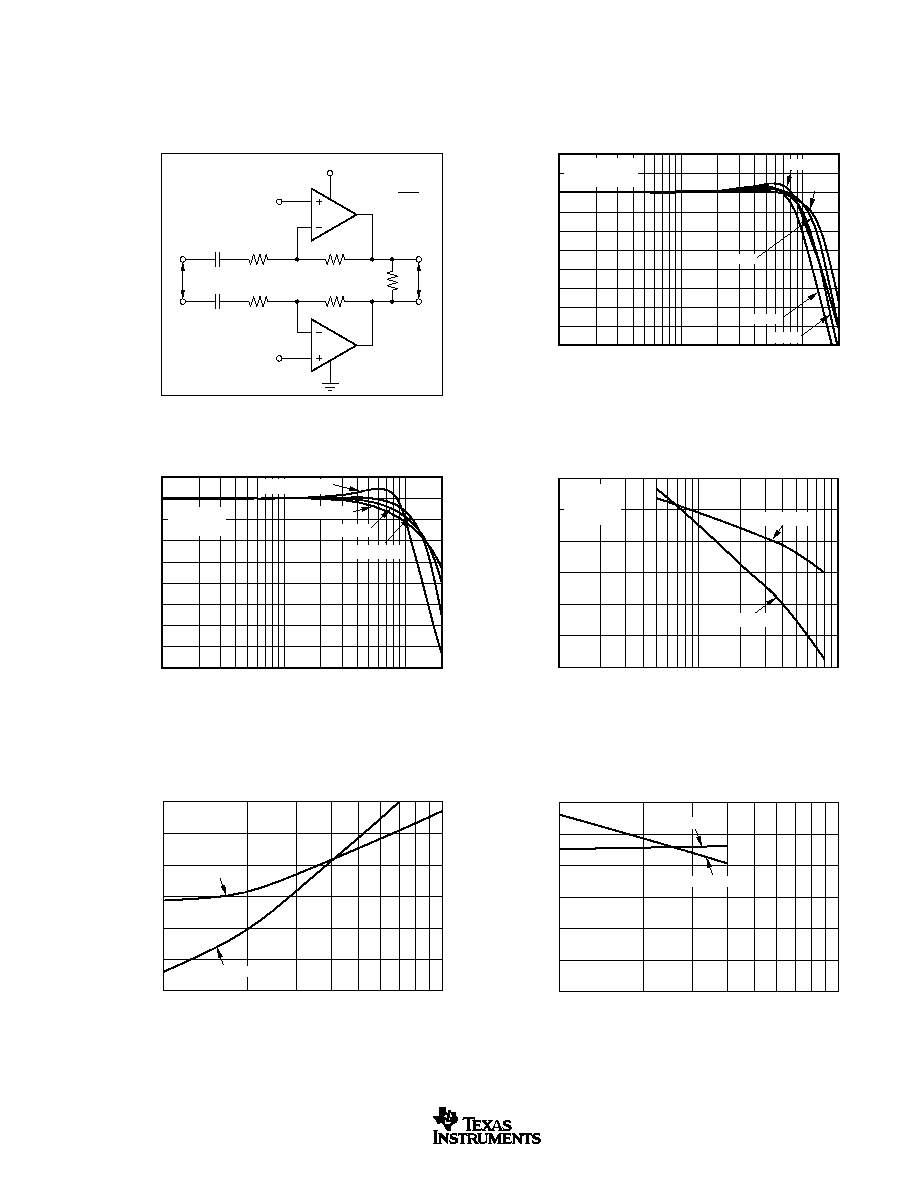
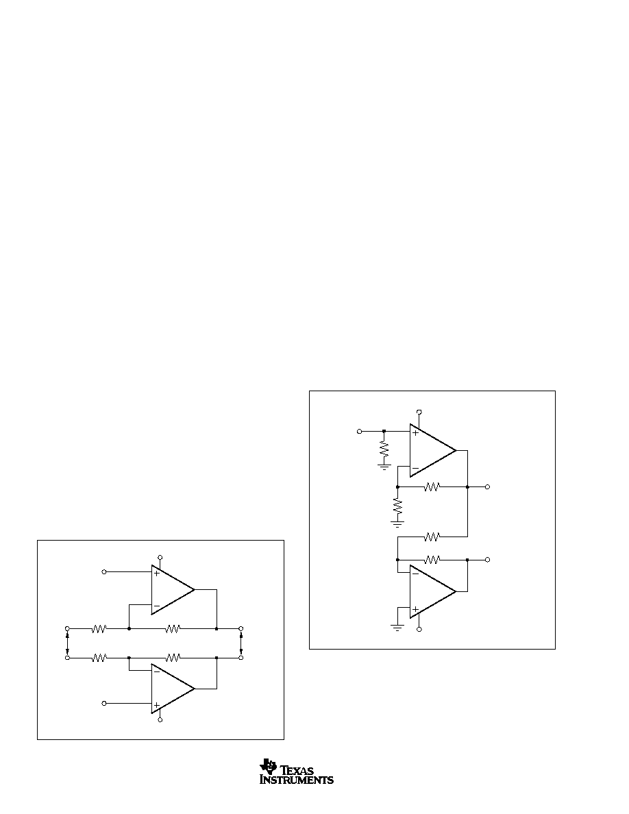
FIGURE 1. DC-Coupled, G = +2V/V, Bipolar Supply Speci-
fications and Test Circuit.
FIGURE 2. DC-Coupled, G = ≠1V/V, Bipolar Supply Specifi-
cations and Test Circuit.
APPLICATIONS INFORMATION
LOW-POWER, CURRENT-FEEDBACK OPERATION
The dual channel OPA2684 gives a new level of perfor-
mance in low-power, current-feedback op amps. Using a
new input stage buffer architecture, the OPA2684 CFB
PLUS
amplifier holds nearly constant AC performance over a wide
gain range. This closed-loop internal buffer gives a very low
and linearized impedance at the inverting node, isolating the
amplifier's AC performance from gain element variations.
This allows both the bandwidth and distortion to remain
nearly constant over gain, moving closer to the ideal current-
feedback performance of gain bandwidth independence.
This low-power amplifier also delivers exceptional output
power--it's
±
4V swing on
±
5V supplies with > 100mA output
drive gives excellent performance into standard video loads
or doubly-terminated 50
cables. This dual-channel device
can provide adequate drive for several emerging differential
driver applications with exceptional power efficiency. Single
+5V supply operation is also supported with similar band-
widths but reduced output power capability. For lower quies-
cent power in a dual CFB
PLUS
amplifier, consider the OPA2683
while for higher output power in a dual current-feedback op
amp, consider the OPA2691 or OPA2677.
Figure 1 shows the DC-coupled, gain of +2, dual power-
supply circuit used as the basis of the
±
5V Electrical and
Typical Characteristics for each channel. For test purposes,
the input impedance is set to 50
with a resistor to ground,
and the output impedance is set to 50
with a series output
resistor. Voltage swings reported in the characteristics are
taken directly at the input and output pins while load powers
(dBm) are defined at a matched 50
load. For the circuit of
Figure 1, the total effective load will be 100
|| 1600
= 94
.
Gain changes are most easily accomplished by simply re-
setting the R
G
value, holding R
F
constant at its recommended
value of 800
.
Figure 2 shows the DC-coupled, gain of ≠1V/V, dual power-
supply circuit used as the basis of the Inverting Typical
Characteristics for each channel. Inverting operation offers
several performance benefits. Since there is no common-
mode signal across the input stage, the slew rate for inverting
operation is typically higher and the distortion performance is
slightly improved. An additional input resistor, R
M
, is included
in Figure 2 to set the input impedance equal to 50
. The
parallel combination of R
M
and R
G
set the input impedance.
As the desired gain increases for the inverting configuration,
R
G
is adjusted to achieve the desired gain, while R
M
is also
adjusted to hold a 50
input match. A point will be reached
where R
G
will equal 50
, R
M
is removed, and the input match
is set by R
G
only. With R
G
fixed to achieve an input match to
50
, increasing R
F
will increase the gain. This will, however,
reduce the achievable bandwidth as the feedback resistor
increases from its recommended value of 800
. If the source
does not require an input match to 50
, either adjust R
M
to
get the desired load, or remove it and let the R
G
resistor
alone provide the input load.
These circuits show
±
5V operation. The same circuit can be
applied with bipolar supplies from
±
2.5V to
±
6V. Internal
supply independent biasing gives nearly the same perfor-
mance for the OPA2684 over this wide range of supplies.
Generally, the optimum feedback resistor value (for nomi-
nally flat frequency response at G = +2) will increase in value
as the total supply voltage across the OPA2684 is reduced
from
±
5V.
See Figure 3 for the AC-coupled, single +5V supply, gain of
+2V/V circuit configuration used as a basis only for the +5V
Electrical and Typical Characteristics for each channel. The
key requirement of broadband single-supply operation is to
maintain input and output signal swings within the useable
voltage ranges at both the input and the output. The circuit
of Figure 3 establishes an input midpoint bias using a simple
resistive divider from the +5V supply (two 10k
resistors) to
the noninverting input. The input signal is then AC-coupled
R
F
800
1/2
OPA2684
+5V
≠5V
50
R
M
50
R
G
800
50
Source
50
Load
V
I
0.1
µ
F
6.8
µ
F
0.1
µ
F
6.8
µ
F
+
+
R
F
800
1/2
OPA2684
+5V
≠5V
50
R
M
53.6
R
G
800
50
Load
50
Source
0.1
µ
F
6.8
µ
F
0.1
µ
F
6.8
µ
F
+
+
V
I
OPA2684
15
SBOS239B
www.ti.com
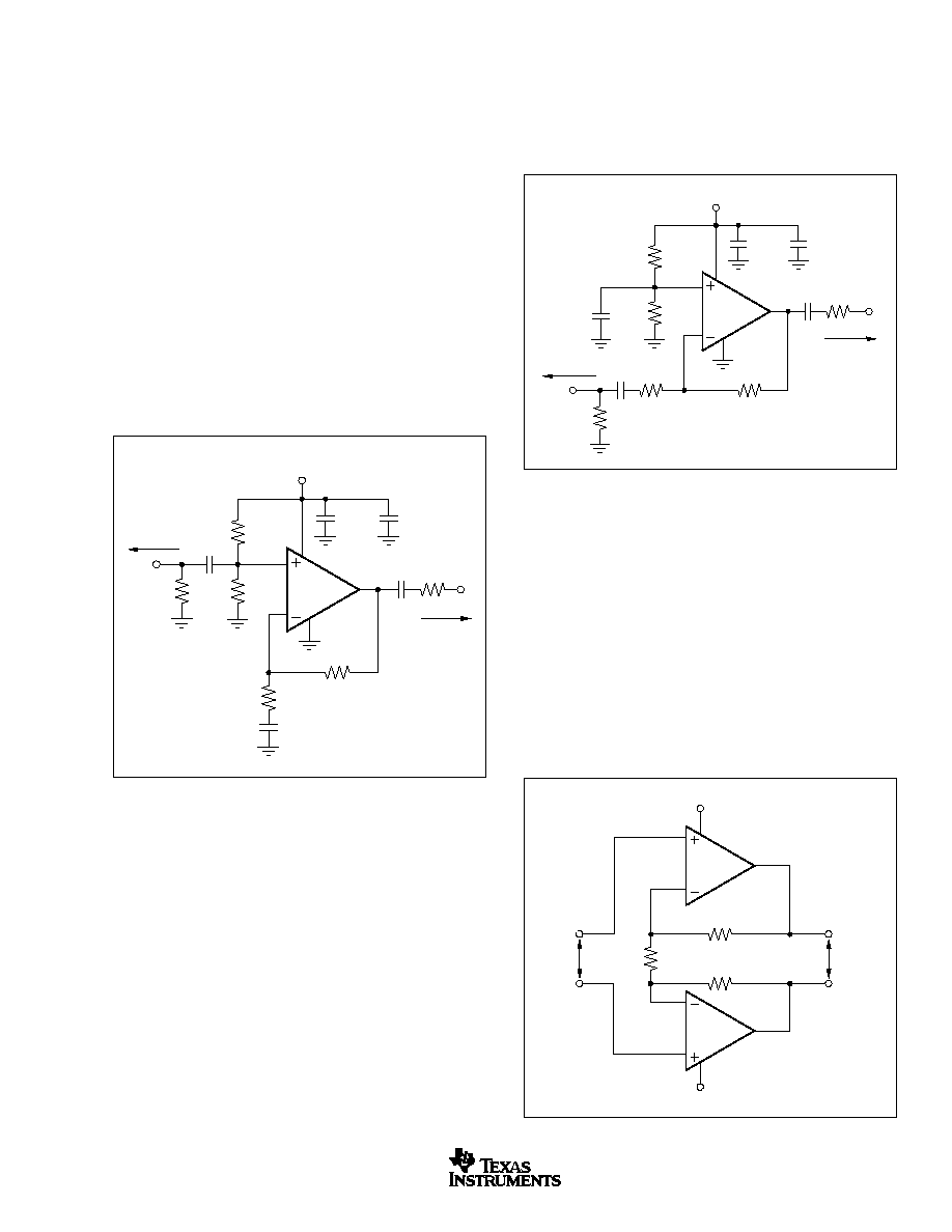
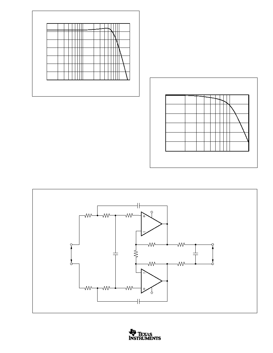
FIGURE 3. AC-Coupled, G = +2V/V, Single-Supply Specifi-
cations and Test Circuit.
FIGURE 4. AC-Coupled, G = ≠1V/V, Single-Supply Specifi-
cations and Test Circuit.
FIGURE 5. Noninverting Differential I/O Amplifier.
into this midpoint voltage bias. The input voltage can swing
to within 1.25V of either supply pin, giving a 2.5Vp-p input
signal range centered between the supply pins. The input
impedance of Figure 3 is set to give a 50
input match. If the
source does not require a 50
match, remove this and drive
directly into the blocking capacitor. The source will then see
the 5k
load of the biasing network. The gain resistor (R
G
)
is AC-coupled, giving the circuit a DC gain of +1, which puts
the noninverting input DC bias voltage (2.5V) on the output
as well. The feedback resistor value has been adjusted from
the bipolar
±
5V supply condition to re-optimize for a flat
frequency response in +5V only, gain of +2, operation. On a
single +5V supply, the output voltage can swing to within
1.0V of either supply pin while delivering more than 70mA
output current giving 3V output swing into 100
(8dBm
maximum at a matched 50
load). The circuit of Figure 3
shows a blocking capacitor driving into a 50
output resistor
then into a 50
load. Alternatively, the blocking capacitor
could be removed if the load is tied to a supply midpoint or
to ground if the DC current required by the load is acceptable.
Figure 4 shows the AC-coupled, single +5V supply, gain of
≠1V/V circuit configuration used as a basis for the +5V
Typical Characteristics for each channel. In this case, the
midpoint DC bias on the noninverting input is also decoupled
with an additional 0.1
µ
F decoupling capacitor. This reduces
the source impedance at higher frequencies for the
noninverting input bias current noise. This 2.5V bias on the
noninverting input pin appears on the inverting input pin and,
since R
G
is DC blocked by the input capacitor, will also
appear at the output pin. One advantage to inverting opera-
tion is that since there is no signal swing across the input
stage, higher slew rates and operation to even lower supply
voltages is possible. To retain a 1Vp-p output capability,
operation down to a 3V supply is allowed. At a +3V supply,
the input stage is saturated, but for the inverting configuration
of a current-feedback amplifier, wideband operation is re-
tained even under this condition.
The circuits of Figure 3 and 4 show single-supply operation
at +5V. These same circuits may be used up to single
supplies of +12V with minimal change in the performance of
the OPA2684.
DIFFERENTIAL INTERFACE APPLICATIONS
Dual op amps are particularly suitable to differential input to
differential output applications. Typically, these fall into either
Analog-to-Digital Converter (ADC) input interface or line
driver applications. Two basic approaches to differential I/O
are noninverting or inverting configurations. Since the output
is differential, the signal polarity is somewhat meaningless--
the noninverting and inverting terminology applies here to
where the input is brought into the OPA2684. Each has its
advantages and disadvantages. Figure 5 shows a basic
starting point for noninverting differential I/O applications.
R
F
1k
1/2
OPA2684
+5V
50
50
Load
50
Source
0.1
µ
F
6.8
µ
F
+
10k
10k
R
M
50
R
G
1k
0.1
µ
F
0.1
µ
F
0.1
µ
F
V
I
R
F
1k
1/2
OPA2684
+5V
50
50
Load
50
Source
0.1
µ
F
0.1
µ
F
6.8
µ
F
+
R
G
1k
10k
10k
0.1
µ
F
V
I
0.1
µ
F
R
M
52.3
R
F
800
R
F
800
1/2
OPA2684
+V
CC
≠V
CC
R
G
V
O
1/2
OPA2684
V
I
OPA2684
16
SBOS239B
www.ti.com
FIGURE 6. Inverting Differential I/O Amplifier.
FIGURE 7. Single to Differential Conversion.
This approach provides for a source termination impedance
that is independent of the signal gain. For instance, simple
differential filters may be included in the signal path right up
to the noninverting inputs without interacting with the gain
setting. The differential signal gain for the circuit of Figure 5 is:
A
D
= 1 + 2 ∑ R
F
/R
G
Since the OPA2684 is a CFB
PLUS
amplifier, its bandwidth is
principally controlled with the feedback resistor value, Figure 5
shows the recommended value of 800
. The differential
gain, however, may be adjusted with considerable freedom
using just the R
G
resistor. In fact, R
G
may be a reactive
network providing a very isolated shaping to the differential
frequency response. Since the inverting inputs of the OPA2684
are very low impedance closed-loop buffer outputs, the R
G
element does not interact with the amplifier's bandwidth,
wide ranges of resistor values and/or filter elements may be
inserted here with minimal amplifier bandwidth interaction.
Various combinations of single-supply or AC-coupled gain
can also be delivered using the basic circuit of Figure 5.
Common-mode bias voltages on the two noninverting inputs
pass on to the output with a gain of 1 since an equal DC
voltage at each inverting node creates no current through
R
G
. This circuit does show a common-mode gain of 1 from
input to output. The source connection should either remove
this common-mode signal if undesired (using an input trans-
former can provide this function), or the common-mode
voltage at the inputs can be used to set the output common-
mode bias. If the low common-mode rejection of this circuit
is problem, the output interface may also be used to reject
that common-mode. For instance, most modern differential
input ADC's reject common-mode signals very well while a
line driver application through a transformer will also attenu-
ate the common-mode signal through to the line.
Figure 6 shows a differential I/O stage configured as an
inverting amplifier. In this case, the gain resistors (R
G
)
become part of the input resistance for the source. This
provides a better noise performance than the noninverting
configuration but does limit the flexibility in setting the input
impedance separately from the gain.
The two noninverting inputs provide an easy common-mode
control input. This is particularly easy if the source is
AC-coupled through either blocking caps or a transformer.
In either case, the common-mode input voltages on the two
noninverting inputs again have a gain of 1 to the output pins
giving particularly easy common-mode control for single-
supply operation. The OPA2684 used in this configuration
does constrain the feedback to the 800
region for best
frequency response. With R
F
fixed, the input resistors may be
adjusted to the desired gain but will also be changing the
input impedance as well. The high frequency common-mode
gain for this circuit from input to output will be the same as
for the signal gain. Again, if the source might include an
undesired common-mode signal, that could be rejected at
the input using blocking caps (for low frequency and DC
common-mode) or a transformer coupling.
DC-COUPLED SINGLE TO DIFFERENTIAL CONVERSION
The previous differential output circuits were set up to re-
ceive a differential input as well. A simple way to provide a
DC-coupled single to differential conversion using a dual op
amp is shown in Figure 7. Here, the output of the first stage
is simply inverted by the second to provide an inverting
version of a single amplifier design. This approach works well
for lower frequencies but will start to depart from ideal
differential outputs as the propagation delay and distortion of
the inverting stage adds significantly to that present at the
noninverting output pin.
R
F
800
R
F
800
R
G
R
G
1/2
OPA2684
+V
CC
≠V
CC
V
CM
V
CM
V
O
1/2
OPA2684
V
I
800
12Vp-p Differential
800
1/2
OPA2684
+5V
≠5V
800
160
1/2
OPA2684
50
1Vp-p
The circuit of Figure 7 is set up for a single-ended gain of 6
to the output of the first amplifier then an inverting gain of
≠1 through the second stage to provide a total differential
gain of 12. See Figure 8 for the SSBW for the circuit of Figure 7.
Large-signal distortion at 12Vp-p output into the 100
differ-
ential load is
80dBc.
OPA2684
17
SBOS239B
www.ti.com
FIGURE 8. Small-Signal Bandwidth for Figure 7.
FIGURE 9. Low-Power, Differential I/O, 4th-Order Butterworth Active Filter.
DIFFERENTIAL ACTIVE FILTER
The OPA2684 can provide a very capable gain block for low-
power active filters. The dual design lends itself very well to
differential active filters. Where the filter topology is looking
for a simple gain function to implement the filter, the
noninverting configuration is preferred to isolate the filter
elements from the gain elements in the design. Figure 9
shows an example of a very low power 10MHz 3rd-order
Butterworth low-pass Sallen-Key filter. Often, these filters are
designed at an amplifier gain of 1 to minimize amplifier
bandwidth interaction with the desired filter shape. Since the
OPA2684 shows minimal bandwidth change with gain, this
would not be a constraint in this design. The example of
24
21
18
15
12
9
6
3
Frequency (MHz)
1
200
10
100
SINGLE TO DIFFERENTIAL CONVERSION
Gain (dB)
V
I
V
O
1/2
OPA2684
1/2
OPA2684
232
50
75pF
22pF
100pF
232
50
100pF
800
20
20
800
≠5V
+5V
357
357
400
Figure 9 designs the filter for a differential gain of 5 using the
OPA2684. The resistor values have been adjusted slightly to
account for the amplifier bandwidth effects.
While this circuit is bipolar, using
±
5V supplies, it can easily
be adapted to single-supply operation. This is typically done
by providing a supply midpoint reference at the noninverting
inputs then adding DC blocking caps at each input and in
series with the amplifier gain resistor, R
G
. This will add two
real zeroes in the response transforming the circuit into a
bandpass. Figure 10 shows the frequency response for the
filter of Figure 9.
14
11
8
5
2
≠1
≠4
Frequency (MHz)
1
20
10
10MHz, 3RD-ORDER BUTTERWORTH, LOW PASS,
FREQUENCY RESPONSE
Differential Gain (dB)
FIGURE 10. Frequency Response for 10MHz, 3rd-Order
Butterworth Low-Pass Filter.
OPA2684
18
SBOS239B
www.ti.com
FIGURE 11. Single-Supply Differential ADC Driver.
FIGURE 12. Measured Harmonic Distortion for the Circuit of
Figure 11.
SINGLE-SUPPLY, HIGH GAIN DIFFERENTIAL
ADC DRIVER
Where a very low power differential I/O interface to a mod-
erate performance ADC is required, the circuit of Figure 11
may be considered. The circuit builds on the inverting differ-
ential I/O configuration of Figure 6 by adding the input
transformer and the output low-pass filter. The input trans-
former provides a single-to-differential conversion where the
input signal is still very low power--it also provides a gain of
2 and removes any common-mode signal from the inputs.
This single +5V design sets a midpoint bias from the supply
at each of the noninverting inputs.
This circuit also includes optional 500
pull-down resistors at
the output. With a 2.5V DC common-mode operating point
(set by V
CM
), this will add 5mA to ground in the output stage.
This essentially powers up the NPN side of the output stage
significantly reducing distortion. It is important for good 2nd-
order distortion to connect the grounds of these two resistors
at the same point to minimize ground plane current for the
differential output signal. Figure 12 shows the measured
2nd- and 3rd-harmonic distortion for the circuit of Figure 11
with and without the pull-down resistors.
Less than ≠65dBc distortion is possible through 5MHz with-
out the pull-down current while this extends to 10MHz using
the two 500
pull-down resistors.
SYNTHETIC IMPEDANCE DSL LINE DRIVER
The need for very low power DSL line drivers is well sup-
ported by the OPA2684 with its high (> 100mA) output
current, low (< 1.2V) headroom, and low supply current
(3.4mA). To further improve power efficiency, simple differ-
ential line drivers are often modified to produce a portion
of the output impedance through positive feedback. This
reduces the voltage swing loss in the remaining discrete
matching resistor leaving more of the available voltage swing
at the input of the transformer. This typically will allow the
transformer turns ratio to be reduced, reducing the peak
output current required. All of this together can reduce the
power dissipated in the line driver while delivering a low
distortion DSL signal to the line.
1/2
OPA2684
1/2
OPA2684
C
L
0.1
µ
F
800
800
+5V
R
S
R
S
200
200
500
ADC
Optional
Optional
10k
10k
50
Source
14.7dB
Noise Figure
Gain = 8V/V
18.1dB
1:2
V
CM
V
CM
500
≠50
≠60
≠70
≠80
≠90
Frequency (MHz)
1
20
10
DISTORTION vs FREQUENCY
Distortion (dBc)
2Vp-p Output
3rd-Harmonic
2nd-Harmonic
No Pull-Down
3rd-Harmonic
2nd-Harmonic
5mA/ch Pull-Down
See Figure 13 for an example design for a +12V single-
supply SHDSL4 line driver where only 27% of the output
impedance is implemented with the physical (18.2
) output
resistors with the remaining 73% implemented with positive
feedback. This synthetic output impedance circuit feeds back
the transformer input voltage to the opposite inverting nodes.
OPA2684
19
SBOS239B
www.ti.com
FIGURE 13. Synthetic Output Impedance xDSL Driver.
BOARD
LITERATURE
PART
REQUEST
PRODUCT
PACKAGE
NUMBER
NUMBER
OPA2684ID
SO-8
DEM-OPA26xU
SBOU003
OPA2684IDCN
SOT23-8
DEM-OPA26xE
SBOU001
TABLE I. Evaluation Module Ordering Information.
DESIGN-IN TOOLS
DEMONSTRATION BOARDS
Two PC boards are available to assist in the initial evaluation
of circuit performance using the OPA2684 in its two package
styles. Both of these are available free as an unpopulated PC
board delivered with descriptive documentation. The sum-
mary information for these boards is shown in Table I.
This example takes a 2Vp-p maximum differential input to a
12.67Vp-p maximum differential voltage on a 135
line using
a 1:1 transformer. For a nominal line at maximum target
power, each output swings a maximum 8Vp-p delivering a
peak 47mA current, on a 12V supply this leaves 2V head-
room on each output with a total amplifier power dissipation
of 163mW. Figure 14 shows the distortion for a full scale
(12.67Vp-p on the line) and 1/2 scale sinusoid signal from
100kHz to 1MHz.
MACROMODELS
Computer simulation of circuit performance using SPICE is
often useful when analyzing the performance of analog
circuits and systems. This is particularly true for higher speed
designs where parasitic capacitance and inductance can
have a major effect on circuit performance. A SPICE model
for the OPA2684 is available in the product folder on the TI
web site (www.ti.com). This is the single channel model for
the OPA684--simply use two of these to implement an
OPA2684 simulation. These models do a good job of predict-
ing small-signal AC and transient performance under a wide
variety of operating conditions. They do not do as well in
predicting the harmonic distortion or dG/dP characteristics.
These models do not attempt to distinguish between the
package types in their small-signal AC performance.
OPERATING SUGGESTIONS
SETTING RESISTOR VALUES TO OPTIMIZE BANDWIDTH
Any current-feedback op amp like the OPA2684 can hold
high bandwidth over signal-gain settings with the proper
adjustment of the external resistor values. A low-power part
like the OPA4684 typically shows a larger change in band-
width due to the significant contribution of the inverting input
impedance to loop-gain changes as the signal gain is changed.
Figure 15 shows a simplified analysis circuit for any current-
feedback amplifier.
FIGURE 14. Harmonic Distortion for Figure 13.
R
F
V
O
R
G
R
I
Z
(S)
i
ERR
i
ERR
V
I
FIGURE 15. Current-Feedback Transfer Function Analysis
Circuit.
≠65
≠70
≠75
≠80
≠85
≠90
≠95
Frequency (MHz)
0.1
1
DIFFERENTIAL DISTORTION vs FREQUENCY
Harmonic Distortion (dBc)
3rd-Harmonic
V
L
= 6.3Vp-p
3rd-Harmonic
V
L
= 12.7Vp-p
2nd-Harmonic
V
L
= 12.7Vp-p
2nd-Harmonic
V
L
= 6.3Vp-p
R
P
1.07k
R
F
800
R
O
18.2
+12V
1/2
OPA2684
1/2
OPA2684
R
F
800
R
O
18.2
12.67Vp-p
135
V
2
max
R
P
1.07k
1:1
2k
+6V
2k
+6V
R
G
931
2Vp-p
max

OPA2684
20
SBOS239B
www.ti.com
The key elements of this current-feedback op amp model
are:
Buffer gain from the noninverting input to the inverting
input
R
I
Buffer output impedance
i
ERR
Feedback error current signal
Z(s)
Frequency dependent open-loop transimpedance
gain from i
ERR
to V
O
The buffer gain is typically very close to 1.00 and is normally
neglected from signal gain considerations. It will, however,
set the CMRR for a single op amp differential amplifier
configuration. For the buffer gain
< 1.0, the CMRR = ≠20
∑ log(1 ≠
). The closed-loop input stage buffer used in the
OPA2684 gives a buffer gain more closely approaching 1.00
and this shows up in a slightly higher CMRR than previous
current-feedback op amps.
R
I
, the buffer output impedance, is a critical portion of the
bandwidth control equation. The OPA2684 reduces this
element to approximately 4.0
using the loop gain of the
closed-loop input buffer stage. This significant reduction in
output impedance, on very low power, contributes signifi-
cantly to extending the bandwidth at higher gains.
A current-feedback op amp senses an error current in the
inverting node (as opposed to a differential input error volt-
age for a voltage-feedback op amp) and passes this on to the
output through an internal frequency dependent
transimpedance gain. The Typical Characteristics show this
open-loop transimpedance response. This is analogous to
the open-loop voltage gain curve for a voltage-feedback op
amp. Developing the transfer function for the circuit of Figure 15
gives Equation 1:
V
V
R
R
R
R
R
R
Z
NG
R
R NG
Z
NG
R
R
O
I
F
G
F
I
F
G
S
F
I
S
F
G
=
+
+
+
+
=
+
+
=
+
1
1
1
1
1
( )
( )
This is written in a loop-gain analysis format where the errors
arising from a non-infinite open-loop gain are shown in the
denominator. If Z(s) were infinite over all frequencies, the
denominator of Equation 1 would reduce to 1 and the ideal
desired signal gain shown in the numerator would be achieved.
The fraction in the denominator of Equation 1 determines the
frequency response. Equation 2 shows this as the loop-gain
equation.
Z
R
R NG
Loop Gain
S
F
I
( )
+
=
If 20 ∑ log(R
F
+ NG ∑ R
I
) were drawn on top of the open-loop
transimpedance plot, the difference between the two would
be the loop gain at a given frequency. Eventually, Z(s) rolls
off to equal the denominator of Equation 2, at which point the
loop gain has reduced to 1 (and the curves have intersected).
This point of equality is where the amplifier's closed-loop
frequency response given by Equation 1 will start to roll off,
and is exactly analogous to the frequency at which the noise
gain equals the open-loop voltage gain for a voltage-feed-
back op amp. The difference here is that the total impedance
in the denominator of Equation 2 may be controlled some-
what separately from the desired signal gain (or NG).
The OPA2684 is internally compensated to give a maximally
flat frequency response for R
F
= 800
at NG = 2 on
±
5V
supplies. That optimum value goes to 1.0k
on a single +5V
supply. Normally, with a current-feedback amplifier, it is
possible to adjust the feedback resistor to hold this band-
width up as the gain is increased. The CFB
PLUS
architecture
has reduced the contribution of the inverting input impedance
to provide exceptional bandwidth to higher gains without
adjusting the feedback resistor value. The Typical Character-
istics show the small-signal bandwidth over gain with a fixed
feedback resistor.
Putting a closed-loop buffer between the noninverting and
inverting inputs does bring some added considerations. Since
the voltage at the inverting output node is now the output of
a locally closed-loop buffer, parasitic external capacitance on
this node can cause frequency response peaking for the
transfer function from the noninverting input voltage to the
inverting node voltage. While it is always important to keep
the inverting node capacitance low for any current-feedback
op amp, it is critically important for the OPA2684. External
layout capacitance in excess of 2pF will start to peak the
frequency response. This peaking can be easily reduced by
then increasing the feedback resistor value--but it is prefer-
able, from a noise and dynamic range standpoint, to keep
that capacitance low, allowing a close to nominal 800
feedback resistor for flat frequency response. Very high
parasitic capacitance values on the inverting node (> 5pF)
can possibly cause input stage oscillation that cannot be
filtered by a feedback element adjustment.
An added consideration is that at very high gains, 2nd-order
effects in the inverting output impedance cause the overall
response to peak up. If desired, it is possible to retain a flat
frequency response at higher gains by adjusting the feed-
back resistor to higher values as the gain is increased. Since
the exact value of feedback that will give a flat frequency
response at high gains depends strongly in inverting and
output node parasitic capacitance values, it is best to experi-
ment in the specific board with increasing values until the
desired flatness (or pulse response shape) is obtained. In
general, increasing R
F
(and adjusting R
G
then to the desired
gain) will move towards flattening the response, while de-
creasing it will extend the bandwidth at the cost of some
peaking. The OPA684 data sheet gives an example of this
optimization of R
F
versus Gain.
OUTPUT CURRENT AND VOLTAGE
The OPA2684 provides output voltage and current capabili-
ties that can support the needs of driving doubly-terminated
50
lines. For a 100
load at the gain of +2, (see Figure 1),
the total load is the parallel combination of the 100
load and
(1)
(2)

OPA2684
21
SBOS239B
www.ti.com
the 1.6k
total feedback network impedance. This 94
load
will require no more than 40mA output current to support the
±
3.8V minimum output voltage swing specified for 100
loads. This is well under the specified minimum +120/≠90mA
specifications over the full temperature range.
The specifications described above, though familiar in the
industry, consider voltage and current limits separately. In
many applications, it is the voltage ∑ current, or V-I product,
which is more relevant to circuit operation. Refer to the
"Output Voltage and Current Limitations" plot in the Typical
Characteristics. The X- and Y-axes of this graph show the
zero-voltage output current limit and the zero-current output
voltage limit, respectively. The four quadrants give a more
detailed view of the OPA2684's output drive capabilities.
Superimposing resistor load lines onto the plot shows the
available output voltage and current for specific loads.
The minimum specified output voltage and current over
temperature are set by worst-case simulations at the cold
temperature extreme. Only at cold startup will the output
current and voltage decrease to the numbers shown in the
Electrical Characteristic tables. As the output transistors
deliver power, their junction temperatures will increase, de-
creasing their V
BE
's (increasing the available output voltage
swing) and increasing their current gains (increasing the
available output current). In steady-state operation, the avail-
able output voltage and current will always be greater than
that shown in the over-temperature specifications since the
output stage junction temperatures will be higher than the
minimum specified operating ambient.
To maintain maximum output stage linearity, no output short-
circuit protection is provided. This will not normally be a
problem since most applications include a series matching
resistor at the output that will limit the internal power dissipa-
tion if the output side of this resistor is shorted to ground.
However, shorting the output pin directly to the adjacent
positive power-supply pin (8 pin packages) can destroy the
amplifier. If additional short-circuit protection is required,
consider a small-series resistor in the power-supply leads.
This will, under heavy output loads, reduce the available
output voltage swing. A 5
series resistor in each power-
supply lead will limit the internal power dissipation to less
than 1W for an output short-circuit, while decreasing the
available output voltage swing only 0.25V for up to 50mA
desired load currents. Always place the 0.1
µ
F power-supply
decoupling capacitors after these supply current limiting
resistors directly on the supply pins.
DRIVING CAPACITIVE LOADS
One of the most demanding and yet very common load
conditions for an op amp is capacitive loading. Often, the
capacitive load is the input of an ADC, including additional
external capacitance which may be recommended to im-
prove ADC linearity. A high-speed, high open-loop gain
amplifier like the OPA2684 can be very susceptible to de-
creased stability and closed-loop response peaking when a
capacitive load is placed directly on the output pin. When the
amplifier's open-loop output resistance is considered, this
capacitive load introduces an additional pole in the signal
path that can decrease the phase margin. Several external
solutions to this problem have been suggested. When the
primary considerations are frequency response flatness, pulse
response fidelity, and/or distortion, the simplest and most
effective solution is to isolate the capacitive load from the
feedback loop by inserting a series isolation resistor between
the amplifier output and the capacitive load. This does not
eliminate the pole from the loop response, but rather shifts it
and adds a zero at a higher frequency. The additional zero
acts to cancel the phase lag from the capacitive load pole,
thus increasing the phase margin and improving stability.
The Typical Characteristics show the recommended "R
S
vs
C
LOAD
" and the resulting frequency response at the load. The
1k
resistor shown in parallel with the load capacitor is a
measurement path and may be omitted. The required series
resistor value may be reduced by increasing the feedback
resistor value from its nominal recommended value. This will
increase the phase margin for the loop gain, allowing a lower
series resistor to be effective in reducing the peaking due
capacitive load. SPICE simulation can be effectively used to
optimize this approach. Parasitic capacitive loads greater
than 5pF can begin to degrade the performance of the
OPA2684. Long PC board traces, unmatched cables, and
connections to multiple devices can easily cause this value
to be exceeded. Always consider this effect carefully, and
add the recommended series resistor as close as possible to
the OPA2684 output pin (see Board Layout Guidelines).
DISTORTION PERFORMANCE
The OPA2684 provides very low distortion in a low-power
part. The CFB
PLUS
architecture also gives two significant
areas of distortion improvement. First, in operating regions
where the 2nd-harmonic distortion due to output stage
nonlinearities is very low (frequencies < 1MHz, low output
swings into light loads) the linearization at the inverting node
provided by the CFB
PLUS
design gives 2nd-harmonic distor-
tions that extend into the ≠90dBc region. Previous current-
feedback amplifiers have been limited to approximately
≠85dBc due to the nonlinearities at the inverting input. The
second area of distortion improvement comes in a distortion
performance that is largely gain independent. To the extent
that the distortion at a particular output power is output stage
dependent, 3rd-harmonics particularly, and to a lesser ex-
tend 2nd-harmonic distortion, is constant as the gain is
increased. This is due to the constant loop gain versus signal
gain provided by the CFB
PLUS
design. As shown in the
Typical Characteristics, while the 3rd-harmonic is constant
with gain, the 2nd-harmonic degrades at higher gains. This
is largely due to board parasitic issues. Slightly imbalanced
load return currents will couple into the gain resistor to cause
a portion of the 2nd-harmonic distortion. At high gains, this
imbalance has more gain to the output giving increased
2nd-harmonic distortion.
Relative to alternative amplifiers with < 2mA supply current,
the OPA2684 holds much lower distortion at higher frequen-
cies (> 5MHz) and to higher gains. Generally, until the
fundamental signal reaches very high frequency or power
levels, the 2nd-harmonic will dominate the distortion with a
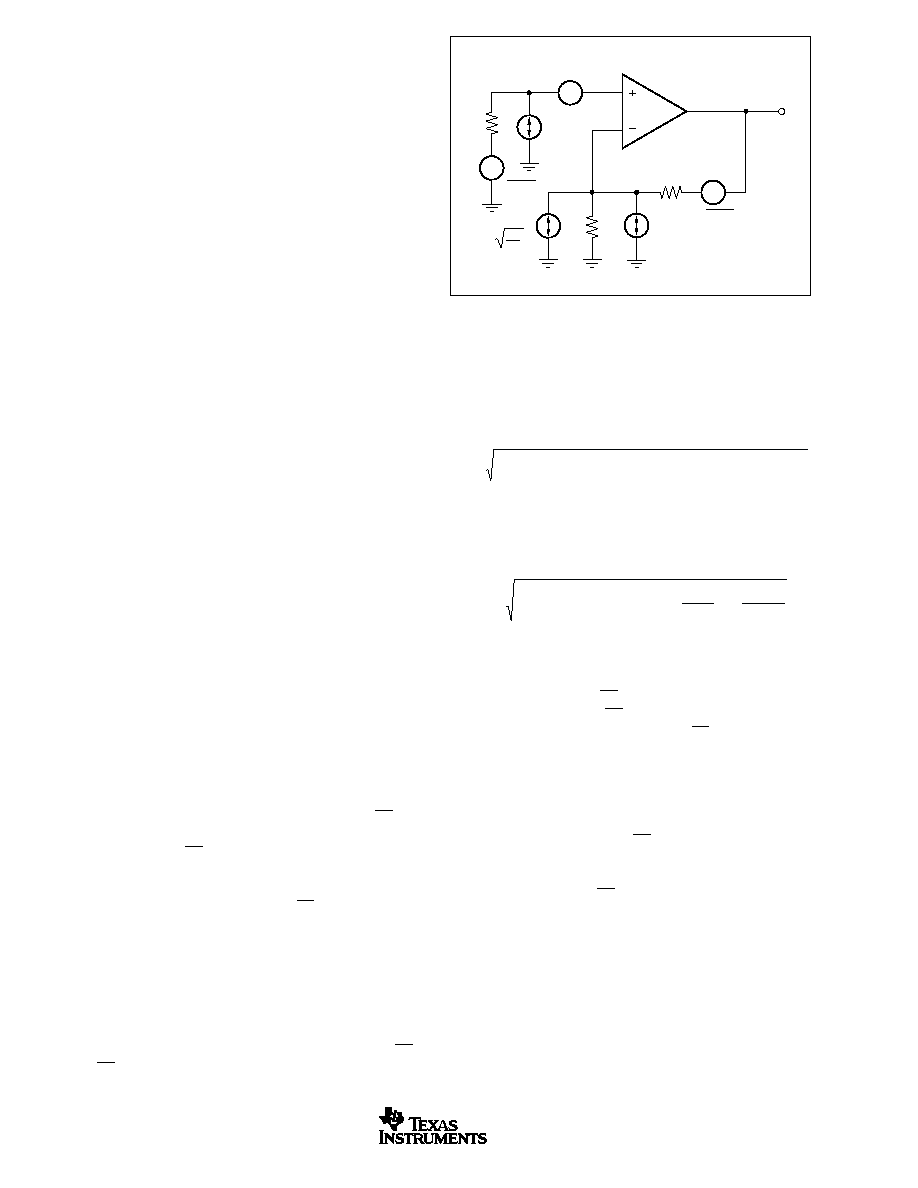
OPA2684
22
SBOS239B
www.ti.com
lower 3rd-harmonic component. Focusing then on the 2nd-
harmonic, increasing the load impedance improves distortion
directly. Remember that the total load includes the feedback
network--in the noninverting configuration (see Figure 1) this
is the sum of R
F
+ R
G
, while in the inverting configuration it
is just R
F
. Also, providing an additional supply decoupling
capacitor (0.1
µ
F) between the supply pins (for bipolar opera-
tion) improves the 2nd-order distortion slightly (3dB to 6dB).
In most op amps, increasing the output voltage swing in-
creases harmonic distortion directly. A low-power part like
the OPA2684 includes quiescent boost circuits to provide the
full-power bandwidth shown in the Typical Characteristics.
These act to increase the bias in a very linear fashion only
when high slew rate or output power are required. This also
acts to actually reduce the distortion slightly at higher output
power levels. The Typical Characteristics show the 2nd-
harmonic holding constant from 500mVp-p to 5Vp-p outputs
while the 3rd-harmonics actually decrease with increasing
output power.
The OPA2684 has an extremely low 3rd-order harmonic
distortion, particularly for light loads and at lower frequen-
cies. This also gives low 2-tone, 3rd-order intermodulation
distortion as shown in the Typical Characteristics. Since the
OPA2684 includes internal power boost circuits to retain
good full-power performance at high frequencies and out-
puts, it does not show a classical 2-tone, 3rd-order
intermodulation intercept characteristic. Instead, it holds rela-
tively low and constant 3rd-order intermodulation spurious
levels over power. The Typical Characteristics show this
spurious level as a dBc below the carrier at fixed center
frequencies swept over single-tone power at a matched 50
load. These spurious levels drop significantly (> 12dB) for
lighter loads than the 100
used in that plot. Converter inputs
for instance will see
82dBc 3rd-order spurious to 10MHz for
full-scale inputs. For even lower 3rd-order intermodulation
distortion to much higher frequencies, consider the OPA2691.
NOISE PERFORMANCE
Wideband current-feedback op amps generally have a higher
output noise than comparable voltage-feedback op amps.
The OPA2684 offers an excellent balance between voltage
and current noise terms to achieve low output noise in a low
power amplifier. The inverting current noise (17pA/
Hz) is
lower most other current-feedback op amps while the input
voltage noise (3.7nV/
Hz) is lower than any unity-gain stable,
comparable slew rate, voltage-feedback op amp. This low
input voltage noise was achieved at the price of higher
noninverting input current noise (9.4pA/
Hz). As long as the
AC source impedance looking out of the noninverting node is
less than 200
, this current noise will not contribute signifi-
cantly to the total output noise. The op amp input voltage
noise and the two input current noise terms combine to give
low output noise under a wide variety of operating conditions.
Figure 16 shows the op amp noise analysis model with all the
noise terms included. In this model, all noise terms are taken
to be noise voltage or current density terms in either nV/
Hz
or pA/
Hz.
The total output spot noise voltage can be computed as the
square root of the sum of all squared output noise voltage
contributors. Equation 3 shows the general form for the
output noise voltage using the terms shown in Figure 16.
(3)
E
E
I
R
kTR
NG
I R
kTR NG
O
NI
BN S
S
BI F
F
=
+
(
)
+
+
(
)
+
2
2
2
2
4
4
Dividing this expression by the noise gain (NG = (1 + R
F
/R
G
))
will give the equivalent input referred spot noise voltage at
the noninverting input as shown in Equation 4.
(4)
E
E
I
R
kTR
I R
NG
kTR
NG
N
NI
BN S
S
BI F
F
=
+
(
)
+
+
+
2
2
2
4
4
Evaluating these two equations for the OPA2684 circuit and
component values (see Figure 1) will give a total output spot
noise voltage of 16.3nV/
Hz and a total equivalent input spot
noise voltage of 8.2 nV/
Hz. This total input referred spot
noise voltage is higher than the 3.7nV/
Hz specification for
the op amp voltage noise alone. This reflects the noise
added to the output by the inverting current noise times the
feedback resistor. As the gain is increased, this fixed output
noise power term contributes less to the total output noise
and the total input referred voltage noise given by Equation 4
will approach just the 3.7nV/
Hz of the op amp itself. For
example, going to a gain of +20 in the circuit of Figure 1,
adjusting only the gain resistor to 42.1
, will give a total input
referred noise of 3.9nV/
Hz. A more complete description of
op amp noise analysis can be found in TI application note
AB-103, "Noise Analysis for High-Speed Op Amps"
(SBOA066), located at www.ti.com.
DC ACCURACY AND OFFSET CONTROL
A current-feedback op amp like the OPA2684 provides
exceptional bandwidth in high gains, giving fast pulse settling
but only moderate DC accuracy. The Electrical Characteris-
tics show an input offset voltage comparable to high slew
rate voltage-feedback amplifiers. The two input bias currents,
4kT
R
G
R
G
R
F
R
S
OPA681
I
BI
E
O
I
BN
4kT = 1.6E ≠20J
at 290
∞
K
E
RS
E
NI
4
kTR
S
4kTR
F
FIGURE 16. Op Amp Noise Analysis Model.

OPA2684
23
SBOS239B
www.ti.com
however, are somewhat higher and are unmatched. Whereas
bias current cancellation techniques are very effective with
most voltage-feedback op amps, they do not generally re-
duce the output DC offset for wideband current-feedback op
amps. Since the two input bias currents are unrelated in both
magnitude and polarity, matching the source impedance
looking out of each input to reduce their error contribution to
the output is ineffective. Evaluating the configuration of
Figure 1, using worst-case +25
∞
C input offset voltage and the
two input bias currents, gives a worst-case output offset
range equal to:
±
(NG ∑ V
OS
) + (I
BN
∑ R
S
/ 2 ∑ NG)
±
(I
BI
∑ R
F
)
where NG = noninverting signal gain
=
±
(2 ∑ 3.8mV)
±
(11
µ
A ∑ 25
∑ 2)
±
(800
∑ 17mA)
=
±
7.6mV + 0.55mV
±
13.6mV
=
±
21.75mV
While the last term, the inverting bias current error, is
dominant in this low-gain circuit, the input offset voltage will
become the dominant DC error term as the gain exceeds
5V/V. Where improved DC precision is required in a high-
speed amplifier, consider the OPA656 single and OPA2822
dual voltage-feedback amplifiers.
THERMAL ANALYSIS
The OPA2684 will not require external heatsinking for most
applications. Maximum desired junction temperature will set
the maximum allowed internal power dissipation as de-
scribed below. In no case should the maximum junction
temperature be allowed to exceed 175
∞
C.
Operating junction temperature (T
J
) is given by T
A
+ P
D
∑
JA
.
The total internal power dissipation (P
D
) is the sum of
quiescent power (P
DQ
) and additional power dissipated in the
output stage (P
DL
) to deliver load power. Quiescent power is
simply the specified no-load supply current times the total
supply voltage across the part. P
DL
will depend on the
required output signal and load but would, for a grounded
resistive load, be at a maximum when the output is fixed at
a voltage equal to 1/2 of either supply voltage (for equal
bipolar supplies). Under this condition P
DL
= V
S
2
/(4 ∑ R
L
)
where R
L
includes feedback network loading.
Note that it is the power in the output stage and not into the
load that determines internal power dissipation.
As an absolute worst-case example, compute the maximum
T
J
using an OPA2684IDCN (SOT23-8 package) in the circuit
of Figure 1 operating at the maximum specified ambient
temperature of +85
∞
C with both outputs driving a grounded
100
load to 2.5V
DC
.
P
D
= 10V ∑ 3.9mA + 2 ∑ (5
2
/(4 ∑ (100
|| 1.6k
))) = 172mW
Maximum T
J
= +85
∞
C + (0.172W ∑ 150
∞
C/W) = 111
∞
C
This maximum operating junction temperature is well below
most system level targets. Most applications will be lower
than this since an absolute worst-case output stage power in
both channels simultaneously was assumed in this calculation.
BOARD LAYOUT GUIDELINES
Achieving optimum performance with a high-frequency am-
plifier like the OPA2684 requires careful attention to board
layout parasitics and external component types. Recommen-
dations that will optimize performance include:
a)
Minimize parasitic capacitance to any AC ground for
all of the signal I/O pins. Parasitic capacitance on the
output and inverting input pins can cause instability; on
the noninverting input, it can react with the source
impedance to cause unintentional bandlimiting. To re-
duce unwanted capacitance, a window around the sig-
nal I/O pins should be opened in all of the ground and
power planes around those pins. Otherwise, ground and
power planes should be unbroken elsewhere on the
board.
b)
Minimize the distance (< 0.25") from the power-supply
pins to high-frequency 0.1
µ
F decoupling capacitors. At
the device pins, the ground and power-plane layout
should not be in close proximity to the signal I/O pins.
Avoid narrow power and ground traces to minimize
inductance between the pins and the decoupling capaci-
tors. The power-supply connections should always be
decoupled with these capacitors. An optional supply de-
coupling capacitor (0.01
µ
F) across the two power sup-
plies (for bipolar operation) will improve 2nd-harmonic
distortion performance. Larger (2.2
µ
F to 6.8
µ
F)
decoupling capacitors, effective at lower frequency,
should also be used on the main supply pins. These may
be placed somewhat farther from the device and may be
shared among several devices in the same area of the
PC board.
c)
Careful selection and placement of external compo-
nents will preserve the high -frequency performance
of the OPA2684. Resistors should be a very low reac-
tance type. Surface-mount resistors work best and allow
a tighter overall layout. Metal film and carbon composi-
tion axially-leaded resistors can also provide good high-
frequency performance. Again, keep their leads and PC-
board trace length as short as possible. Never use
wirewound type resistors in a high-frequency applica-
tion. Since the output pin and inverting input pin are the
most sensitive to parasitic capacitance, always position
the feedback and series output resistor, if any, as close
as possible to the output pin. Other network compo-
nents, such as noninverting input termination resistors,
should also be placed close to the package. The fre-
quency response is primarily determined by the feed-
back resistor value as described previously. Increasing
its value will reduce the peaking at higher gains, while
decreasing it will give a more peaked frequency re-
sponse at lower gains. The 800
feedback resistor used
in the Electrical Characteristics at a gain of +2 on
±
5V
supplies is a good starting point for design. Note that an
800
feedback resistor, rather than a direct short, is
required for the unity-gain follower application. A cur-
rent-feedback op amp requires a feedback resistor even
in the unity-gain follower configuration to control stability.
OPA2684
24
SBOS239B
www.ti.com
FIGURE 17. Internal ESD Protection.
d)
Connections to other wideband devices on the board
may be made with short direct traces or through on-
board transmission lines. For short connections, con-
sider the trace and the input to the next device as a
lumped capacitive load. Relatively wide traces (50mils to
100mils) should be used, preferably with ground and
power planes opened up around them. Estimate the
total capacitive load and set R
S
from the plot of recom-
mended "Rs vs C
LOAD
". Low parasitic capacitive loads
(< 5pF) may not need an R
S
since the OPA2684 is
nominally compensated to operate with a 2pF parasitic
load. If a long trace is required, and the 6dB signal loss
intrinsic to a doubly-terminated transmission line is ac-
ceptable, implement a matched impedance transmis-
sion line using microstrip or stripline techniques (consult
an ECL design handbook for microstrip and stripline
layout techniques). A 50
environment is normally not
necessary on board, and in fact a higher impedance
environment will improve distortion, as shown in the
distortion versus load plots. With a characteristic board
trace impedance defined based on board material and
trace dimensions, a matching series resistor into the
trace from the output of the OPA2684 is used, as well as
a terminating shunt resistor at the input of the destina-
tion device. Remember also that the terminating imped-
ance will be the parallel combination of the shunt resistor
and the input impedance of the destination device; this
total effective impedance should be set to match the
trace impedance. The high output voltage and current
capability of the OPA2684 allows multiple destination
devices to be handled as separate transmission lines,
each with their own series and shunt terminations. If the
6dB attenuation of a doubly-terminated transmission line
is unacceptable, a long trace can be series-terminated
at the source end only. Treat the trace as a capacitive
load in this case and set the series resistor value as
shown in the plot of "Rs vs C
LOAD
". This will not preserve
signal integrity as well as a doubly-terminated line. If the
input impedance of the destination device is low, there
will be some signal attenuation due to the voltage divider
formed by the series output into the terminating imped-
ance.
e)
Socketing a high-speed part like the OPA2684 is not
recommended. The additional lead length and pin-to-
pin capacitance introduced by the socket can create an
extremely troublesome parasitic network which can make
it almost impossible to achieve a smooth, stable fre-
quency response. Best results are obtained by soldering
the OPA2684 onto the board.
INPUT AND ESD PROTECTION
The OPA2684 is built using a very high-speed complemen-
tary bipolar process. The internal junction breakdown volt-
ages are relatively low for these very small geometry de-
vices. These breakdowns are reflected in the Absolute Maxi-
mum Ratings table where an absolute maximum 13V across
the supply pins is reported. All device pins have limited ESD
protection using internal diodes to the power supplies as
shown in Figure 17.
These diodes provide moderate protection to input overdrive
voltages above the supplies as well. The protection diodes
can typically support 30mA continuous current. Where higher
currents are possible (e.g., in systems with
±
15V supply parts
driving into the OPA2684), current-limiting series resistors
should be added into the two inputs. Keep these resistor
values as low as possible since high values degrade both
noise performance and frequency response.
External
Pin
+V
CC
≠V
CC
Internal
Circuitry
OPA2684
25
SBOS239B
www.ti.com
PACKAGE DRAWINGS
D (R-PDSO-G**)
PLASTIC SMALL-OUTLINE PACKAGE
8 PINS SHOWN
8
0.197
(5,00)
A MAX
A MIN
(4,80)
0.189
0.337
(8,55)
(8,75)
0.344
14
0.386
(9,80)
(10,00)
0.394
16
DIM
PINS **
4040047/E 09/01
0.069 (1,75) MAX
Seating Plane
0.004 (0,10)
0.010 (0,25)
0.010 (0,25)
0.016 (0,40)
0.044 (1,12)
0.244 (6,20)
0.228 (5,80)
0.020 (0,51)
0.014 (0,35)
1
4
8
5
0.150 (3,81)
0.157 (4,00)
0.008 (0,20) NOM
0
∞
≠ 8
∞
Gage Plane
A
0.004 (0,10)
0.010 (0,25)
0.050 (1,27)
NOTES: A. All linear dimensions are in inches (millimeters).
B. This drawing is subject to change without notice.
C. Body dimensions do not include mold flash or protrusion, not to exceed 0.006 (0,15).
D. Falls within JEDEC MS-012

OPA2684
26
SBOS239B
www.ti.com
PACKAGE DRAWINGS (Cont.)
DCN (R-PDSO-G8)
PLASTIC SMALL-OUTLINE
C
4202106/A 03/01
3,00
2,80
3,00
2,60
1,50
1,75
Area
0,28
0,45
0
∞
≠10
∞
0,09
0,20
1,30
0,90
0,10
0,60
Index
0,00
0,15
≠A≠
0,65
0,90
1,45
1,95 REF
NOTES: A. All linear dimensions are in millimeters.
B. This drawing is subject to change without notice.
C. Foot length measured reference to flat foot surface
parallel to Datum A.
D. Package outline exclusive of mold flash, metal burr and
dambar protrusion/intrusion.
E. Package outline inclusive of solder plating.
F. A visual index feature must be located within the
cross-hatched area.

PACKAGING INFORMATION
ORDERABLE DEVICE
STATUS(1)
PACKAGE TYPE
PACKAGE DRAWING
PINS
PACKAGE QTY
OPA2684ID
ACTIVE
SOIC
D
8
100
OPA2684IDCNR
ACTIVE
SSOP
DCN
8
3000
OPA2684IDCNT
ACTIVE
SSOP
DCN
8
250
OPA2684IDR
ACTIVE
SOIC
D
8
2500
(1) The marketing status values are defined as follows:
ACTIVE: Product device recommended for new designs.
LIFEBUY: TI has announced that the device will be discontinued, and a lifetime-buy period is in effect.
NRND: Not recommended for new designs. Device is in production to support existing customers, but TI does not recommend using this part in
a new design.
PREVIEW: Device has been announced but is not in production. Samples may or may not be available.
OBSOLETE: TI has discontinued the production of the device.
PACKAGE OPTION ADDENDUM
www.ti.com
3-Oct-2003

IMPORTANT NOTICE
Texas Instruments Incorporated and its subsidiaries (TI) reserve the right to make corrections, modifications,
enhancements, improvements, and other changes to its products and services at any time and to discontinue
any product or service without notice. Customers should obtain the latest relevant information before placing
orders and should verify that such information is current and complete. All products are sold subject to TI's terms
and conditions of sale supplied at the time of order acknowledgment.
TI warrants performance of its hardware products to the specifications applicable at the time of sale in
accordance with TI's standard warranty. Testing and other quality control techniques are used to the extent TI
deems necessary to support this warranty. Except where mandated by government requirements, testing of all
parameters of each product is not necessarily performed.
TI assumes no liability for applications assistance or customer product design. Customers are responsible for
their products and applications using TI components. To minimize the risks associated with customer products
and applications, customers should provide adequate design and operating safeguards.
TI does not warrant or represent that any license, either express or implied, is granted under any TI patent right,
copyright, mask work right, or other TI intellectual property right relating to any combination, machine, or process
in which TI products or services are used. Information published by TI regarding third-party products or services
does not constitute a license from TI to use such products or services or a warranty or endorsement thereof.
Use of such information may require a license from a third party under the patents or other intellectual property
of the third party, or a license from TI under the patents or other intellectual property of TI.
Reproduction of information in TI data books or data sheets is permissible only if reproduction is without
alteration and is accompanied by all associated warranties, conditions, limitations, and notices. Reproduction
of this information with alteration is an unfair and deceptive business practice. TI is not responsible or liable for
such altered documentation.
Resale of TI products or services with statements different from or beyond the parameters stated by TI for that
product or service voids all express and any implied warranties for the associated TI product or service and
is an unfair and deceptive business practice. TI is not responsible or liable for any such statements.
Following are URLs where you can obtain information on other Texas Instruments products and application
solutions:
Products
Applications
Amplifiers
amplifier.ti.com
Audio
www.ti.com/audio
Data Converters
dataconverter.ti.com
Automotive
www.ti.com/automotive
DSP
dsp.ti.com
Broadband
www.ti.com/broadband
Interface
interface.ti.com
Digital Control
www.ti.com/digitalcontrol
Logic
logic.ti.com
Military
www.ti.com/military
Power Mgmt
power.ti.com
Optical Networking
www.ti.com/opticalnetwork
Microcontrollers
microcontroller.ti.com
Security
www.ti.com/security
Telephony
www.ti.com/telephony
Video & Imaging
www.ti.com/video
Wireless
www.ti.com/wireless
Mailing Address:
Texas Instruments
Post Office Box 655303 Dallas, Texas 75265
Copyright
2003, Texas Instruments Incorporated