Document Outline
- FEATURES
- APPLICATIONS
- DESCRIPTION
- OPA2690 RELATED PRODUCTS
- ABSOLUTE MAXIMUM RATINGS
- PACKAGE/ORDERING INFORMATION
- PIN CONFIGURATION
- ELECTRICAL CHARACTERISTICS: V S = +/-5V
- ELECTRICAL CHARACTERISTICS: V S = +5V
- TYPICAL CHARACTERISTICS: V S = +/-5V
- TYPICAL CHARACTERISTICS: V S = +5V
- APPLICATIONS INFORMATION
- WIDEBAND VOLTAGE-FEEDBACK OPERATION
- SINGLE-SUPPLY ADC INTERFACE
- HIGH- PERFORMANCE DAC TRANSIMPEDANCE AMPLIFIER
- WIDEBAND VIDEO MULTIPLEXING
- HIGH-SPEED DELAY CIRCUIT
- DIFFERENTIAL RECEIVER/DRIVER
- SINGLE-SUPPLY MFB DIFFERENTIAL ACTIVE FILTER: 10 MHz BUTTERWORTH CONFIGURATION
- SINGLE-SUPPLY DIFFERENTIAL ADC DRIVER
- DESIGN-IN TOOLS
- DEMONSTRATION BOARDS
- MACROMODELS
- OPERATING SUGGESTIONS
- OPTIMIZING RESISTOR VALUES
- BANDWIDTH vs GAIN: NONINVERTING OPERATION
- INVERTING AMPLIFIER OPERATION
- OUTPUT CURRENT AND VOLTAGE
- DRIVING CAPACITIVE LOADS
- DISTORTION PERFORMANCE
- NOISE PERFORMANCE
- DC ACCURACY AND OFFSET CONTROL
- DISABLE OPERATION (SO-14 Package Only)
- THERMAL ANALYSIS
- BOARD LAYOUT GUIDELINES
- PACKAGE DRAWING
- D (R-PDSO-G**)PLASTIC SMALL-OUTLINE PACKAGE
OPA2690
SBOS238B ≠ JUNE 2002 ≠ REVISED JULY 2003
www.ti.com
Copyright © 2002-2003, Texas Instruments Incorporated
Dual, Wideband, Voltage-Feedback
OPERATIONAL AMPLIFIER With Disable
FEATURES
q
FLEXIBLE SUPPLY RANGE:
+5V to +12V Single Supply
±
2.5V to
±
6V Dual Supplies
q
WIDEBAND +5V OPERATION: 220MHz (G = 2)
q
HIGH OUTPUT CURRENT: 190mA
q
OUTPUT VOLTAGE SWING:
±
4.0V
q
HIGH SLEW RATE: 1800V/
µ
s
q
LOW SUPPLY CURRENT: 5.5mA/ch
q
LOW DISABLED CURRENT: 100
µ
A/ch
APPLICATIONS
q
VIDEO LINE DRIVING
q
xDSL LINE DRIVER/RECEIVER
q
HIGH-SPEED IMAGING CHANNELS
q
ADC BUFFERS
q
PORTABLE INSTRUMENTS
q
TRANSIMPEDANCE AMPLIFIERS
q
ACTIVE FILTERS
DESCRIPTION
The OPA2690 represents a major step forward in unity-gain
stable, voltage-feedback op amps. A new internal architec-
ture provides slew rate and full-power bandwidth previously
found only in wideband current-feedback op amps. A new
output stage architecture delivers high currents with a mini-
mal headroom requirement. These give exceptional single-
supply operation. Using a single +5V supply, the OPA2690
can deliver a 1V to 4V output swing with over 120mA drive
current and 150MHz bandwidth. This combination of fea-
tures makes the OPA2690 an ideal RGB line driver or single-
supply Analog-to-Digital Converter (ADC) input driver.
The low 5.5mA/ch supply current of the OPA2690 is pre-
cisely trimmed at +25
∞
C. This trim, along with low tempera-
ture drift, ensures lower maximum supply current than
competing products. System power may be reduced further
using the optional disable control pin. Leaving this disable
pin open, or holding it HIGH, will operate the OPA2690I-
14D normally. If pulled LOW, the OPA2690I-14D supply
current drops to less than 200
µ
A/ch while the output goes
into a high-impedance state.
OPA2690 RELATED PRODUCTS
SINGLES
DUALS
TRIPLES
Voltage-Feedback
OPA690
OPA2680
OPA3690
Current-Feedback
OPA691
OPA2691
OPA3691
Fixed Gain
OPA692
--
OPA3692
OPA2
690
OPA2
690
0.1
µ
F
IN
+5V
10pF
0.1
µ
F
10pF
499
499
Clock
IN
REFT
REFB
ADS825
10-Bit
40MSPS
1/2
OPA2690
+5V
+2.5V
+2.5V
+2.5V
1/2
OPA2690
V
IN
1k
1k
499
499
35
35
2k
100
100pF
2k
2.5V
CM
2Vp-p
PRODUCTION DATA information is current as of publication date.
Products conform to specifications per the terms of Texas Instruments
standard warranty. Production processing does not necessarily include
testing of all parameters.
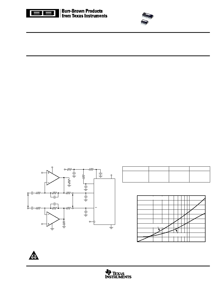
Single-Supply Differential ADC Driver
HARMONIC DISTORTION vs FREQUENCY
FOR THE SINGLE-SUPPLY ADC DRIVER
Harmonic Distortion (dBc)
Frequency (MHz)
≠50
≠55
≠60
≠65
≠70
≠75
≠80
≠85
≠90
≠95
≠100
1
10
20
3rd-Harmonic
2nd-Harmonic
2V
PP
Differential Output
Please be aware that an important notice concerning availability, standard warranty, and use in critical applications of
Texas Instruments semiconductor products and disclaimers thereto appears at the end of this data sheet.
All trademarks are the property of their respective owners.
OPA2690
2
SBOS238B
www.ti.com
ABSOLUTE MAXIMUM RATINGS
(1)
Power Supply ...............................................................................
±
6.5V
DC
Internal Power Dissipation ....................... See Thermal Analysis Section
Differential Input Voltage ..................................................................
±
1.2V
Input Voltage Range ............................................................................
±
V
S
Storage Temperature Range: D, 14D ............................ ≠40
∞
C to +125
∞
C
Lead Temperature (soldering, 10s) .............................................. +300
∞
C
Junction Temperature (T
J
) ........................................................... +150
∞
C
ESD Resistance: HBM .................................................................... 2000V
CDM .................................................................... 1500V
MM ........................................................................ 200V
NOTE: (1) Stresses above these ratings may cause permanent damage.
Exposure to absolute maximum conditions for extended periods may degrade
device reliability. These are stress ratings only, and functional operation of the
device at these or any other conditions beyond those specified is not implied.
ELECTROSTATIC
DISCHARGE SENSITIVITY
This integrated circuit can be damaged by ESD. Texas Instru-
ments recommends that all integrated circuits be handled with
appropriate precautions. Failure to observe proper handling
and installation procedures can cause damage.
ESD damage can range from subtle performance degrada-
tion to complete device failure. Precision integrated circuits
may be more susceptible to damage because very small
parametric changes could cause the device not to meet its
published specifications.
SPECIFIED
PACKAGE
TEMPERATURE
PACKAGE
ORDERING
TRANSPORT
PRODUCT
PACKAGE-LEAD
DESIGNATOR
(1)
RANGE
MARKING
NUMBER
MEDIA, QUANTITY
OPA2690
SO-8
D
≠40
∞
C to +85
∞
C
OPA2690
OPA2690ID
Rails, 100
"
"
"
"
"
OPA2690IDR
Tape and Reel, 2500
OPA2690
SO-14
D
≠40
∞
C to +85
∞
C
OPA2690
OPA2690I-14D
Rails, 58
"
"
"
"
"
OPA2690I-14DR
Tape and Reel, 2500
NOTE: (1) For the most current specifications and package information, refer to our web site at www.ti.com.
PACKAGE/ORDERING INFORMATION
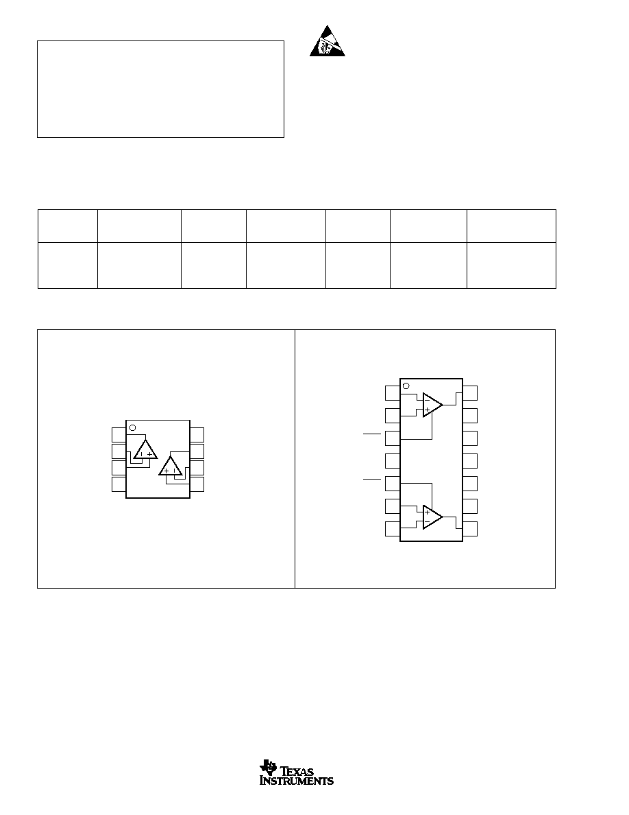
PIN CONFIGURATION
Top View
SO
Top View
SO
1
2
3
4
8
7
6
5
+V
S
Out B
≠In B
+In B
Out A
≠In A
+In A
≠V
S
A
B
1
2
3
4
5
6
7
14
13
12
11
10
9
8
≠In A
+In A
DIS A
≠V
S
DIS B
+In B
≠In B
Out A
NC
NC
+V
S
NC
NC
Out B

OPA2690
3
SBOS238B
www.ti.com
ELECTRICAL CHARACTERISTICS:
V
S
=
±
5V
Boldface limits are tested at +25
∞
C.
R
F
= 402
, R
L
= 100
,
and G = +2 (see Figure 1 for AC performance only), unless otherwise noted.
OPA2690ID, I-14D
TYP
MIN/MAX OVER TEMPERATURE
0
∞
C to
≠40
∞
C to
MIN/
TEST
PARAMETER
CONDITIONS
+25
∞
C
+25
∞
C
(1)
70
∞
C
(2)
+85
∞
C
(2)
UNITS
MAX
LEVEL
(3)
AC PERFORMANCE (see Figure 1)
Small-Signal Bandwidth
G = +1, V
O
= 0.5V
PP
, R
F
= 25
500
MHz
typ
C
G = +2, V
O
= 0.5V
PP
220
165
160
150
MHz
min
B
G = +10, V
O
= 0.5V
PP
30
20
19
18
MHz
min
B
Gain-Bandwidth Product
G
10
300
200
190
180
MHz
min
B
Bandwidth for 0.1dB Gain Flatness
G = +2, V
O
< 0.5V
PP
30
MHz
typ
C
Peaking at a Gain of +1
V
O
< 0.5V
PP
4
dB
typ
C
Large-Signal Bandwidth
G = +2, V
O
= 5V
PP
200
MHz
typ
C
Slew Rate
G = +2, 4V Step
1800
1400
1200
900
V/
µ
s
min
C
Rise-and-Fall Time
G = +2, V
O
= 0.5V Step
1.4
ns
typ
C
G = +2, V
O
= 5V Step
2.8
ns
typ
C
Settling Time to 0.02%
G = +2, V
O
= 2V Step
12
ns
typ
C
0.1%
G = +2, V
O
= 2V Step
8
ns
typ
C
Harmonic Distortion
G = +2, f = 5MHz, V
O
= 2V
PP
2nd-Harmonic
R
L
= 100
≠68
≠64
≠62
≠60
dBc
max
R
L
500
≠77
≠70
≠68
≠66
dBc
max
B
3rd-Harmonic
R
L
= 100
≠70
≠68
≠66
≠64
dBc
max
B
R
L
500
≠81
≠78
≠76
≠75
dBc
max
B
Input Voltage Noise
f > 1MHz
5.5
nV/
Hz
typ
C
Input Current Noise
f > 1MHz
3.1
pA/
Hz
typ
C
Differential Gain
G = +2, NTSC, V
O
= 1.4Vp, R
L
= 150
0.06
%
typ
C
Differential Phase
G = +2, NTSC, V
O
= 1.4Vp, R
L
= 150
0.03
deg
typ
C
Channel-to-Channel Crosstalk
f = 5MHz, Input Referred
≠85
dBc
typ
C
DC PERFORMANCE
(4)
Open-Loop Voltage Gain (A
OL
)
V
O
= 0V, R
L
= 100
69
58
56
54
dB
min
A
Input Offset Voltage
V
CM
= 0V
±
1.0
±
4.5
±
5.0
±
5.2
mV
max
A
Average Offset Voltage Drift
V
CM
= 0V
±
12
±
12
µ
V/
∞
C
max
B
Input Bias Current
V
CM
= 0V
+5
±
10
±
11
±
12
µ
A
max
A
Average Bias Current Drift (magnitude)
V
CM
= 0V
±
20
±
40
nA/
∞
C
max
B
Input Offset Current
V
CM
= 0V
±
0.1
±
1.0
±
1.4
±
1.6
µ
A
max
A
Average Offset Current Drift
V
CM
= 0V
±
1
±
1.5
nA/
∞
C
max
B
INPUT
Common-Mode Input Range (CMIR)
(5)
±
3.5
±
3.4
±
3.3
±
3.2
V
min
A
Common-Mode Rejection Ratio (CMRR)
V
CM
=
±
1V
68
60
57
56
dB
min
A
Input Impedance
Differential-Mode
V
CM
= 0
190
|| 0.6
k
|| pF
typ
C
Common-Mode
V
CM
= 0
3.2
|| 0.9
M
|| pF
typ
C
OUTPUT
Voltage Output Swing
No Load
±
4.0
±
3.8
±
3.7
±
3.6
V
min
A
100
Load
±
3.9
±
3.7
±
3.6
±
3.3
V
min
A
Current Output, Sourcing
V
O
= 0
+190
+160
+140
+100
mA
min
A
Current Output, Sinking
V
O
= 0
≠190
≠160
≠140
≠100
mA
min
A
Short-Circuit Current
V
O
= 0
±
250
mA
typ
C
Closed-Loop Output Impedance
G = +2, f = 100kHz
0.04
typ
C
(1) Junction temperature = ambient for +25
∞
C specifications.
(2) Junction temperature = ambient at low temperature limit; junction temperature = ambient +15
∞
C at high temperature limit for over temperature specifications.
(3) Test Levels: (A) 100% tested at +25
∞
C. Over-temperature limits by characterization and simulation. (B) Limits set by characterization and simulation. (C) Typical
value only for information.
(4) Current is considered positive out-of-node. V
CM
is the input common-mode voltage.
(5) Tested < 3dB below minimum CMRR specification at
±
CMIR limits.

OPA2690
4
SBOS238B
www.ti.com
ELECTRICAL CHARACTERISTICS:
V
S
=
±
5V (Cont.)
Boldface limits are tested at +25
∞
C.
R
F
= 402
, R
L
= 100
,
and G = +2 (see Figure 1 for AC performance only), unless otherwise noted.
OPA2690ID, I-14D
TYP
MIN/MAX OVER TEMPERATURE
0
∞
C to
≠40
∞
C to
MIN/
TEST
PARAMETER
CONDITIONS
+25
∞
C
+25
∞
C
(1)
70
∞
C
(2)
+85
∞
C
(2)
UNITS
MAX
LEVEL
(3 )
(1) Junction temperature = ambient for +25
∞
C specifications.
(2) Junction temperature = ambient at low temperature limit; junction temperature = ambient +15
∞
C at high temperature limit for over temperature specifications.
(3) Test Levels: (A) 100% tested at +25
∞
C. Over-temperature limits by characterization and simulation. (B) Limits set by characterization and simulation. (C) Typical
value only for information.
(4) Current is considered positive out-of-node. V
CM
is the input common-mode voltage.
(5) Tested < 3dB below minimum CMRR specification at
±
CMIR limits.
DISABLE (SO-14 Only)
Disabled LOW
Power-Down Supply Current (+V
S
)
V
DIS
= 0, Both Channels
≠200
≠400
≠480
≠520
µ
A
max
A
Disable Time
V
IN
= 1V
DC
200
ns
typ
C
Enable Time
V
IN
= 1V
DC
25
ns
typ
C
Off Isolation
G = +2, 5MHz
70
dB
typ
C
Output Capacitance in Disable
4
pF
typ
C
Turn-On Glitch
G = +2, R
L
= 150
, V
IN
= 0
±
50
mV
typ
C
Turn-Off Glitch
G = +2, R
L
= 150
, V
IN
= 0
±
20
mV
typ
C
Enable Voltage
3.3
3.5
3.6
3.7
V
min
A
Disable Voltage
1.8
1.7
1.6
1.5
V
max
A
Control Pin Input Bias Current (V
DIS
)
V
DIS
= 0, Each Channel
75
130
150
160
µ
A
max
A
POWER SUPPLY
Specified Operating Voltage
±
5
V
typ
C
Maximum Operating Voltage Range
±
6
±
6
±
6
V
max
A
Maximum Quiescent Current (2 Channels)
V
S
=
±
5V
11
11.6
12.2
12.6
mA
max
A
Minimum Quiescent Current (2 Channels)
V
S
=
±
5V
11
10.6
10.2
9.4
mA
min
A
Power-Supply Rejection Ratio (+PSRR)
Input Referred
75
68
66
64
dB
min
A
THERMAL CHARACTERISTICS
Specified Operating Range D, 14D Package
≠40 to +85
∞
C
typ
C
Thermal Resistance,
JA
Junction-to-Ambient
D
SO-8
125
∞
C/W
typ
C
14D
SO-14
100
∞
C/W
typ
C
OPA2690
5
SBOS238B
www.ti.com
ELECTRICAL CHARACTERISTICS:
V
S
= +5V
Boldface limits are tested at +25
∞
C.
R
F
= 402
, R
L
= 100
to V
S
/2
,
and G = +2 (see Figure 2 for AC performance only), unless otherwise noted.
OPA2690ID, I-14D
TYP
MIN/MAX OVER TEMPERATURE
0
∞
C to
≠40
∞
C to
MIN/
TEST
PARAMETER
CONDITIONS
+25
∞
C
+25
∞
C
(1)
70
∞
C
(2)
+85
∞
C
(2)
UNITS
MAX
LEVEL
(3)
AC PERFORMANCE (see Figure 2)
Small-Signal Bandwidth
G = +1, V
O
< 0.5V
PP
, R
F
=
±
25
400
MHz
typ
C
G = +2, V
O
< 0.5V
PP
190
150
145
140
MHz
min
B
G = +10, V
O
< 0.5V
PP
25
18
17
16
MHz
min
B
Gain-Bandwidth Product
G
10
250
180
170
160
MHz
min
B
Bandwidth for 0.1dB Gain Flatness
G = +2, V
O
< 0.5V
PP
20
MHz
typ
C
Peaking at a Gain of +1
V
O
< 0.5V
PP
5
dB
typ
C
Large-Signal Bandwidth
G = +2, V
O
= 2V
PP
220
MHz
typ
C
Slew Rate
G = +2, 2V Step
1000
700
670
550
V/
µ
s
min
B
Rise-and-Fall Time
G = +2, V
O
= 0.5V Step
1.6
ns
typ
C
G = +2, V
O
= 2V Step
2.0
ns
typ
C
Settling Time to 0.02%
G = +2, V
O
= 2V Step
12
ns
typ
C
0.1%
G = +2, V
O
= 2V Step
8
ns
typ
C
Harmonic Distortion
G = +2, f = 5MHz, V
O
= 2V
PP
2nd-Harmonic
R
L
= 100
to V
S
/2
≠65
≠60
≠59
≠56
dBc
max
B
R
L
500
to V
S
/2
≠75
≠70
≠68
≠66
dBc
max
B
3rd-Harmonic
R
L
= 100
to V
S
/2
≠68
≠64
≠62
≠60
dBc
max
B
R
L
500
to V
S
/2
≠77
≠73
≠71
≠70
dBc
max
B
Input Voltage Noise
f > 1MHz
5.6
nV/
Hz
typ
C
Input Current Noise
f > 1MHz
3.2
pA/
Hz
typ
C
Differential Gain
G = +2, NTSC, V
O
= 1.4Vp, R
L
= 150 to V
S
/2
0.06
%
typ
C
Differential Phase
G = +2, NTSC, V
O
= 1.4Vp, R
L
= 150 to V
S
/2
0.02
deg
typ
C
DC PERFORMANCE
(4)
Open-Loop Voltage Gain
V
O
= 2.5V, R
L
= 100
to 2.5V
63
56
54
52
dB
min
A
Input Offset Voltage
V
CM
= 2.5V
±
1.0
±
4.5
±
4.8
±
5.2
mV
max
A
Average Offset Voltage Drift
V
CM
= 2.5V
±
10
±
10
µ
V/
∞
C
max
B
Input Bias Current
V
CM
= 2.5V
+5
±
10
±
11
±
12
µ
A
max
A
Average Bias Current Drift
V
CM
= 2.5V
±
20
±
40
nA/
∞
C
max
B
(magnitude)
Input Offset Current
V
CM
= 2.5V
±
0.3
±
1.0
±
1.4
±
1.6
µ
A
max
A
Average Offset Current Drift
V
CM
= 2.5V
±
7
±
9
nA/
∞
C
max
B
INPUT
Least Positive Input Voltage
(5)
1.5
1.6
1.7
1.8
V
max
A
Most Positive Input Voltage
(5)
3.5
3.4
3.3
3.2
V
min
A
Common-Mode Rejection Ratio (CMRR)
V
CM
= 2.5V
±
0.5V
63
58
56
54
dB
min
A
Input Impedance
Differential-Mode
V
CM
= 2.5V
92 || 1.4
k
|| pF
typ
C
Common-Mode
V
CM
= 2.5V
2.2 || 1.5
M
|| pF
typ
C
OUTPUT
Most Positive Output Voltage
No Load
4
3.8
3.6
3.5
V
min
A
R
L
= 100
to 2.5V
3.9
3.7
3.5
3.4
V
min
A
Least Positive Output Voltage
No Load
1
1.2
1.4
1.5
V
max
A
R
L
= 100
to 2.5V
1.1
1.3
1.5
1.7
V
max
A
Current Output, Sourcing
+160
+120
+100
+80
mA
min
A
Current Output, Sinking
≠160
≠120
≠100
≠80
mA
min
A
Short-Circuit Current
V
O
= V
S
/2
±
250
mA
typ
C
Closed-Loop Output Impedance
G = +2, f = 100kHz
0.04
typ
C
(1) Junction temperature = ambient for +25
∞
C specifications.
(2) Junction temperature = ambient at low temperature limit; junction temperature = ambient +15
∞
C at high temperature limit for over temperature specifications.
(3) Test Levels: (A) 100% tested at +25
∞
C. Over-temperature limits by characterization and simulation. (B) Limits set by characterization and simulation. (C) Typical
value only for information.
(4) Current is considered positive out-of-node. V
CM
is the input common-mode voltage.
(5) Tested < 3dB below minimum CMRR specification at
±
CMIR limits.

OPA2690
6
SBOS238B
www.ti.com
ELECTRICAL CHARACTERISTICS:
V
S
= +5V (Cont.)
Boldface limits are tested at +25
∞
C.
R
F
= 402
, R
L
= 100
to V
S
/2
,
and G = +2 (see Figure 2 for AC performance only), unless otherwise noted.
OPA2690ID, I-14D
TYP
MIN/MAX OVER TEMPERATURE
0
∞
C to
≠40
∞
C to
MIN/
TEST
PARAMETER
CONDITIONS
+25
∞
C
+25
∞
C
(1)
70
∞
C
(2)
+85
∞
C
(2)
UNITS
MAX
LEVEL
(3)
DISABLE (SO-14 Only)
Disabled LOW
Power-Down Supply Current (+V
S
)
V
DIS
= 0, Both Channels
≠200
≠400
≠480
≠520
µ
A
max
A
Off Isolation
G = +2, 5MHz
65
dB
typ
C
Output Capacitance in Disable
4
pF
typ
C
Turn-On Glitch
G = +2, R
L
= 150
, V
IN
= V
S
/2
±
50
mV
typ
C
Turn-Off Glitch
G = +2, R
L
= 150
, V
IN
= V
S
/2
±
20
mV
typ
C
Enable Voltage
3.3
3.5
3.6
3.7
V
min
A
Disable Voltage
1.8
1.7
1.6
1.5
V
max
A
Control Pin Input Bias Current (V
DIS
)
V
DIS
= 0, Each Channel
75
130
150
160
µ
A
typ
C
POWER SUPPLY
Specified Single-Supply Operating Voltage
5
V
typ
C
Maximum Single-Supply Operating Voltage
12
12
12
V
max
B
Maximum Quiescent Current (2 Channels)
V
S
= +5V
9.8
10.4
10.9
11.4
mA
max
A
Minimum Quiescent Current (2 Channels)
V
S
= +5V
9.8
9.4
8.6
8
mA
min
A
Power-Supply Rejection Ratio (+PSRR)
Input Referred
72
dB
typ
C
TEMPERATURE RANGE
Specification: D, 14D
≠40 to +85
∞
C
typ
C
Thermal Resistance,
JA
Junction-to-Ambient
D
SO-8
125
∞
C/W
typ
C
14D
SO-14
100
∞
C/W
typ
C
(1) Junction temperature = ambient for +25
∞
C specifications.
(2) Junction temperature = ambient at low temperature limit; junction temperature = ambient +15
∞
C at high temperature limit for over temperature specifications.
(3) Test Levels: (A) 100% tested at +25
∞
C. Over-temperature limits by characterization and simulation. (B) Limits set by characterization and simulation. (C) Typical
value only for information.
(4) Current is considered positive out-of-node. V
CM
is the input common-mode voltage.
(5) Tested < 3dB below minimum CMRR specification at
±
CMIR limits.

OPA2690
7
SBOS238B
www.ti.com
TYPICAL CHARACTERISTICS: V
S
=
±
5V
At T
A
= +25
∞
C, G = +2, R
F
= 402
, and R
L
= 100
(see Figure 1 for AC performance only), unless otherwise noted.
SMALL-SIGNAL FREQUENCY RESPONSE
Normalized Gain (3dB/div)
Frequency (MHz)
0.7
10
100
700
6
3
0
≠3
≠6
≠9
≠12
≠15
V
O
= 0.5V
PP
G = +1
R
F
= 25
G = 2
G = 5
G = 10
LARGE-SIGNAL FREQUENCY RESPONSE
10
0.5
1
100
500
Frequency (MHz)
Gain (3dB/div)
9
6
3
0
≠3
≠6
V
O
= 4V
PP
V
O
= 7V
PP
V
O
= 2V
PP
V
O
= 1V
PP
SMALL-SIGNAL PULSE RESPONSE
Time (5ns/div)
400
300
200
100
0
≠100
≠200
≠300
≠400
G = +2
V
O
= 0.5V
PP
Output V
oltage (100mV/div)
LARGE-SIGNAL PULSE RESPONSE
Time (5ns/div)
Output V
oltage (1V/div)
+4
+3
+2
+1
0
≠1
≠2
≠3
≠4
G = +2
V
O
= 5V
PP
COMPOSITE VIDEO dG/dP
dG/dP (%/degree)
Number of 150
Loads
1
2
3
4
0.200
0.175
0.150
0.125
0.100
0.075
0.050
0.025
0
dG
dG
dP
dP
No Pull-Down
With 1.3k
Pull-Down
1/2
OPA2690
402
≠5V
+5V
75
Video In
402
Optional
1.3k
Pull-Down
CHANNEL-TO-CHANNEL CROSSTALK
Crosstalk (5dB/div)
Frequency (MHz)
1
10
100
≠55
≠60
≠65
≠70
≠75
≠80
≠85
≠90
≠95
≠100
Input Referred
OPA2690
8
SBOS238B
www.ti.com
TYPICAL CHARACTERISTICS: V
S
=
±
5V
(Cont.)
At T
A
= +25
∞
C, G = +2, R
F
= 402
, and R
L
= 100
(see Figure 1 for AC performance only), unless otherwise noted.
HARMONIC DISTORTION vs LOAD RESISTANCE
Harmonic Distortion (dBc)
Resistance (
)
100
1000
≠60
≠65
≠70
≠75
≠80
≠85
≠90
V
O
= 2V
PP
f = 5MHz
3rd-Harmonic
2nd-Harmonic
5MHz HARMONIC DISTORTION vs SUPPLY VOLTAGE
Harmonic Distortion (dBc)
Supply Voltage (
±
V
S
)
2.0
2.5
3.0
3.5
4.0
4.5
5.0
5.5
6.0
≠60
≠65
≠70
≠75
≠80
3rd-Harmonic
2nd-Harmonic
V
O
= 2V
PP
R
L
= 100
f = 5MHz
HARMONIC DISTORTION vs FREQUENCY
Harmonic Distortion (dBc)
Frequency (MHz)
0.1
1
10
20
≠40
≠50
≠60
≠70
≠80
≠90
≠100
V
O
= 2V
PP
R
L
= 100
2nd-Harmonic
3rd-Harmonic
HARMONIC DISTORTION vs OUTPUT VOLTAGE
Harmonic Distortion (dBc)
Output Voltage Swing (Vp-p)
0.1
1
5
≠60
≠65
≠70
≠75
≠80
R
L
= 100
f = 5MHz
3rd-Harmonic
2nd-Harmonic
HARMONIC DISTORTION vs NONINVERTING GAIN
Harmonic Distortion (dBc)
Noninverting Gain (V/V)
1
10
20
≠40
≠50
≠60
≠70
≠80
≠90
3rd-Harmonic
2nd-Harmonic
V
O
= 2V
PP
R
L
= 100
f = 5MHz
HARMONIC DISTORTION vs INVERTING GAIN
Harmonic Distortion (dBc)
Inverting Gain (V/V)
1
10
20
≠40
≠50
≠60
≠70
≠80
V
O
= 2V
PP
R
L
= 100
f = 5MHz
3rd-Harmonic
2nd-Harmonic
OPA2690
9
SBOS238B
www.ti.com
TYPICAL CHARACTERISTICS: V
S
=
±
5V
(Cont.)
At T
A
= +25
∞
C, G = +2, R
F
= 402
, and R
L
= 100
(see Figure 1 for AC performance only), unless otherwise noted.
INPUT VOLTAGE AND CURRENT NOISE DENSITY
Current Noise (pA/
Hz)
Voltage Noise (nV/
Hz)
Frequency (Hz)
100
1M
100k
10k
1k
10M
100
10
1
Voltage Noise 5.5nV/
Hz
Current Noise 3.1pA/
Hz
2-TONE, 3RD-ORDER
INTERMODULATION SPURIOUS
3rd-Order Spurious Level (dBc)
Single-Tone Load Power (dBm)
≠8
≠6
≠4
≠2
0
2
4
6
8
10
≠30
≠35
≠40
≠45
≠50
≠55
≠60
≠65
≠70
≠75
20MHz
10MHz
50MHz
Load Power at Matched 50
Load,
see Figure 1
RECOMMENDED R
S
vs CAPACITIVE LOAD
R
S
(
)
Capacitive Load (pF)
10
100
1000
80
70
60
50
40
30
20
10
0
FREQUENCY RESPONSE vs CAPACITIVE LOAD
Gain-to-Capacitive Load (dB)
Frequency (20MHz/div)
0
100
120
140
160
180
20
40
60
80
200
9
6
3
0
≠3
≠6
≠9
402
1k
402
R
S
C
L
V
IN
V
OUT
1/2
OPA2690
1k
is optional.
C
L
= 22pF
C
L
= 47pF
C
L
= 100pF
C
L
= 10pF
G = +2
LARGE-SIGNAL DISABLE/ENABLE RESPONSE
Time (50ns/div)
Output V
oltage (0.4V/div)
2.0
1.6
1.2
0.8
0.4
0
V
DIS
(2V/div)
6
4
2
0
G = +2
V
IN
= +1V
V
DIS
Output Voltage
Each Channel
SO-14
Package
Only
DISABLE FEEDTHROUGH vs FREQUENCY
Frequency (Hz)
Feedthrough (5dB/div)
≠45
≠50
≠55
≠60
≠65
≠70
≠75
≠80
≠85
≠90
≠95
≠100
Forward
Reverse
V
DIS = 0
100k
1M
10M
100M

OPA2690
10
SBOS238B
www.ti.com
TYPICAL CHARACTERISTICS: V
S
=
±
5V
(Cont.)
At T
A
= +25
∞
C, G = +2, R
F
= 402
, and R
L
= 100
(see Figure 1 for AC performance only), unless otherwise noted.
OUTPUT VOLTAGE AND CURRENT LIMITATIONS
V
O
(V)
I
O
(mA)
≠300
≠200
≠100
0
100
200
300
5
4
3
2
1
0
≠1
≠2
≠3
≠4
≠5
Output Current Limited
1W Internal
Power Limit
One Channel
Only
1W Internal
Power Limit
Output Current Limit
100
Load Line
50
Load Line
25
Load Line
TYPICAL DC DRIFT OVER TEMPERATURE
Input Offset Voltage (mV)
Input Bias and Offset Currents (
µ
A)
Ambient Temperature (
∞
C)
≠50
≠25
0
25
50
75
100
125
2
1.5
1
0.5
0
≠0.5
≠1
≠1.5
≠2
20
10
0
≠10
≠20
Input Offset Current (I
OS
)
Input Offset Voltage (V
OS
)
Input Bias Current (I
B
)
COMMON-MODE REJECTION RATIO AND
POWER-SUPPLY REJECTION RATIO vs FREQUENCY
PSRR (dB)
CMRR (dB)
Frequency (MHz)
10k
1M
100k
10M
100M
100
90
80
70
60
50
40
30
20
10
0
CMRR
+PSRR
≠PSRR
SUPPLY AND OUTPUT CURRENTS vs TEMPERATURE
Supply Current (2mA/div)
Output Current (50mA/div)
Ambient Temperature (
∞
C)
≠50
≠25
0
25
50
75
100
125
14
12
10
8
6
4
250
200
150
100
50
0
Sourcing Output Current
Sinking Output Current
Quiescent Supply Current
CLOSED-LOOP OUTPUT IMPEDANCE vs FREQUENCY
Output Impedance (
)
Frequency (Hz)
10k
1M
100k
10M
100M
10
1
0.1
0.01
1/2
OPA2690
402
+5V
≠5V
200
402
Z
O
OPEN-LOOP GAIN AND PHASE
Open-Loop Gain (dB)
Frequency (MHz)
1k
1M
100k
10k
10M
1G
100M
70
60
50
40
30
20
10
0
≠10
≠20
Open-Loop Phase (
∞
)
0
≠30
≠60
≠90
≠120
≠150
≠180
≠210
≠240
≠270
Open-Loop Gain
Open-Loop Phase

OPA2690
11
SBOS238B
www.ti.com
TYPICAL CHARACTERISTICS: V
S
= +5V
At T
A
= +25
∞
C, G = +2, R
F
= 402
, and R
L
= 100
(see Figure 2 for AC performance only), unless otherwise noted.
SMALL-SIGNAL FREQUENCY RESPONSE
Normalized Gain (3dB/div)
Frequency (Hz)
0.7 1
10
700
100
6
3
0
≠3
≠6
≠9
G = +1
R
F
= 25
G = +2
G = +5
G = +10
V
O
= 0.5V
PP
LARGE-SIGNAL FREQUENCY RESPONSE
Gain (3dB/div)
Frequency (MHz)
0.5
1
10
500
100
9
6
3
0
≠3
≠6
V
O
= 2V
PP
V
O
= 3V
PP
V
O
= 1V
PP
SMALL-SIGNAL PULSE RESPONSE
Time (5ns/div)
Output V
oltage (100mV/div)
2.9
2.8
2.7
2.6
2.5
2.4
2.3
2.2
2.1
G = +2
V
O
= 0.5V
PP
LARGE-SIGNAL PULSE RESPONSE
Time (5ns/div)
Output V
oltage (400mV/div)
4.1
3.7
3.3
2.9
2.5
2.1
1.7
1.3
0.9
G = +2
V
O
= 2V
PP
RECOMMENDED R
S
vs CAPACITIVE LOAD
R
S
(
)
Capacitive Load (pF)
1
10
100
1000
50
45
40
35
30
25
20
15
10
5
0
FREQUENCY RESPONSE vs CAPACITIVE LOAD
Gain-to-Capacitive Load (dB)
Frequency (20MHz/div)
0
100
120
140
160
180
20
40
60
80
200
9
6
3
0
≠3
≠6
≠9
C
L
= 22pF
C
L
= 47pF
C
L
= 100pF
C
L
= 10pF
402
58
714
0.1
µ
F
714
714
402
R
S
C
L
V
IN
+5V
V
OUT
+5V
1/2
OPA2690
OPA2690
12
SBOS238B
www.ti.com
TYPICAL CHARACTERISTICS: V
S
= +5V
(Cont.)
At T
A
= +25
∞
C, G = +2, R
F
= 402
, and R
L
= 100
(see Figure 2 for AC performance only), unless otherwise noted.
HARMONIC DISTORTION vs LOAD RESISTANCE
Harmonic Distortion (dBc)
Resistance (
)
100
1000
≠60
≠65
≠70
≠75
≠80
3rd-Harmonic
V
O
= 2V
PP
f = 5MHz
2nd-Harmonic
HARMONIC DISTORTION vs FREQUENCY
Harmonic Distortion (dBc)
Frequency (MHz)
0.1
1
10
20
≠40
≠50
≠60
≠70
≠80
≠90
≠100
V
O
= 2V
PP
R
L
= 100
to 2.5V
2nd-Harmonic
3rd-Harmonic
HARMONIC DISTORTION vs OUTPUT VOLTAGE
Harmonic Distortion (dBc)
Output Voltage Swing (V
PP
)
0.1
1
3
≠60
≠65
≠70
≠75
≠80
3rd-Harmonic
2nd-Harmonic
R
L
= 100
to 2.5V
f = 5MHz
2-TONE, 3RD-ORDER
INTERMODULATION SPURIOUS
3rd-Order Spurious Level (dBc)
Single-Tone Load Power (dBm)
≠14
≠12
≠10
≠8
≠6
≠4
≠2
0
2
≠30
≠35
≠40
≠45
≠50
≠55
≠60
≠65
≠70
≠75
20MHz
10MHz
50MHz
Load Power at Matched 50
Load, see Figure 2
OPA2690
13
SBOS238B
www.ti.com
APPLICATIONS INFORMATION
WIDEBAND VOLTAGE-FEEDBACK OPERATION
The OPA2690 provides an exceptional combination of high
output power capability in a dual, wideband, unity-gain stable,
voltage-feedback op amp using a new high slew rate input
stage. Typical differential input stages used for voltage-feed-
back op amps are designed to steer a fixed-bias current to the
compensation capacitor, setting a limit to the achievable slew
rate. The OPA2690 uses a new input stage that places the
transconductance element between two input buffers, using
their output currents as the forward signal. As the error voltage
increases across the two inputs, an increasing current is
delivered to the compensation capacitor. This provides very
high slew rate (1800V/
µ
s) while consuming relatively low
quiescent current (5.5mA/ch). This exceptional full-power per-
formance comes at the price of a slightly higher input noise
voltage than alternative architectures. The 5.5nV/
Hz input
voltage noise for the OPA2690 is exceptionally low for this
type of input stage.
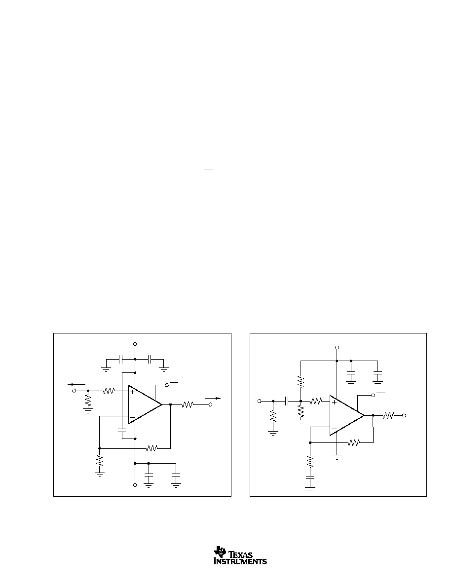
Figure 1 shows the DC-coupled, gain of +2, dual power-supply
circuit configuration used as the basis of the
±
5V Electrical and
Typical Characteristics. This is for one channel; the other
channel is connected similarly. For test purposes, the input
impedance is set to 50
with a resistor to ground and the
output impedance is set to 50
with a series output resistor.
Voltage swings reported in the electrical characteristics are
taken directly at the input and output pins, whereas output
powers (dBm) are at the matched 50
load. For the circuit of
Figure 1, the total effective load will be 100
|| 804
. The
disable control line (SO-14 package only) is typically left open
for normal amplifier operation. Two optional components are
included in Figure 1. An additional resistor (175
) is included
in series with the noninverting input. Combined with the 25
DC source resistance looking back towards the signal genera-
tor, this gives an input bias current cancelling resistance that
matches the 200
source resistance seen at the inverting
input (see the DC Accuracy and Offset Control section). In
addition to the usual power-supply decoupling capacitors to
ground, a 0.1
µ
F capacitor is included between the two power-
supply pins. In practical PC board layouts, this optional-added
capacitor will typically improve the 2nd-harmonic distortion
performance by 3dB to 6dB.
Figure 2 shows the AC-coupled, gain of +2, single-supply
circuit configuration used as the basis of the +5V Electrical and
Typical Characteristics. Though not a rail-to-rail design, the
OPA2690 requires minimal input and output voltage headroom
compared to other very wideband voltage-feedback op amps.
It will deliver a 3Vp-p output swing on a single +5V supply with
> 150MHz bandwidth. The key requirement of broadband
single-supply operation is to maintain input and output signal
swings within the usable voltage ranges at both the input and
the output. The circuit of Figure 2 establishes an input midpoint
bias using a simple resistive divider from the +5V supply (two
698
resistors). Separate bias networks would be required at
each input. The input signal is then AC-coupled into the
midpoint voltage bias. The input voltage can swing to within
1.5V of either supply pin, giving a 2V
PP
input signal range
centered between the supply pins. The input impedance match-
ing resistor (59
) used for testing is adjusted to give a 50
input load when the parallel combination of the biasing divider
network is included. Again, an additional resistor (50
in this
case) is included directly in series with the noninverting input.
This minimum recommended value provides part of the DC
source resistance matching for the noninverting input bias
current. It is also used to form a simple parasitic pole to roll off
the frequency response at very high frequencies (> 500MHz)
using the input parasitic capacitance. The gain resistor (R
G
) is
FIGURE 1. DC-Coupled, G = +2, Bipolar Supply, Specifica-
tion and Test Circuit.
FIGURE 2. AC-Coupled, G = +2, Single-Supply Specification
and Test Circuit.
1/2
OPA2690
+5V
+V
S
≠V
S
+
DIS
≠5V
50
Load
50
175
50
V
O
V
D
V
I
50
Source
R
G
402
R
F
402
+
6.8
µ
F
0.1
µ
F
6.8
µ
F
0.1
µ
F
0.1
µ
F
1/2
OPA2690
+5V
+V
S
DIS
V
S
/2
698
100
V
O
V
D
V
I
698
50
R
G
402
R
F
402
0.1
µ
F
0.1
µ
F
59
+
6.8
µ
F
0.1
µ
F

OPA2690
14
SBOS238B
www.ti.com
AC-coupled, giving the circuit a DC gain of +1, which puts the
input DC bias voltage (2.5V) on the output as well. The output
voltage can swing to within 1V of either supply pin while
delivering > 100mA output current. A demanding 100
load to
a midpoint bias is used in this characterization circuit. The new
output stage circuit used in the OPA2690 can deliver large
bipolar output currents into this midpoint load with minimal
crossover distortion, as shown in the +5V supply harmonic
distortion plots.
SINGLE-SUPPLY ADC INTERFACE
Most modern, high-performance ADCs (such as the ADS8xx
and ADS9xx series from Texas Instruments) operate on a
single +5V (or lower) power supply. It has been a consider-
able challenge for single-supply op amps to deliver a low
distortion input signal at the ADC input for signal frequencies
exceeding 5MHz. The high slew rate, exceptional output
swing, and high linearity of the OPA2690 make it an ideal
single-supply ADC driver. The circuit on the front page shows
one possible interface particularly suited to differential I/O,
AC-coupled requirements. Figure 3 shows the AC-coupled
test circuit of Figure 2 modified for a capacitive (ADC) load
and with an optional output pull-down resistor (R
B
). This
circuit would be suitable to dual-channel ADC driving with a
single-ended I/O.
The OPA2690 in the circuit of Figure 3 provides > 200MHz
bandwidth for a 2V
PP
output swing. Minimal 3rd-harmonic
distortion or 2-tone, 3rd-order intermodulation distortion will be
observed due to the very low crossover distortion in the
OPA2690 output stage. The limit of output Spurious-Free
Dynamic Range (SFDR) will be set by the 2nd-harmonic
distortion. Without R
B
, the circuit of Figure 3 measured at
10MHz shows an SFDR of 57dBc. This can be improved by
pulling additional DC bias current (I
B
) out of the output stage
through the optional R
B
resistor to ground (the output midpoint
is at 2.5V for Figure 3). Adjusting I
B
gives the improvement in
SFDR shown in Figure 4. SFDR improvement is achieved for
I
B
values up to 5mA, with worse performance for higher
values. Using the dual OPA2690 in an I/Q receiver channel will
give matched AC performance through high frequencies.
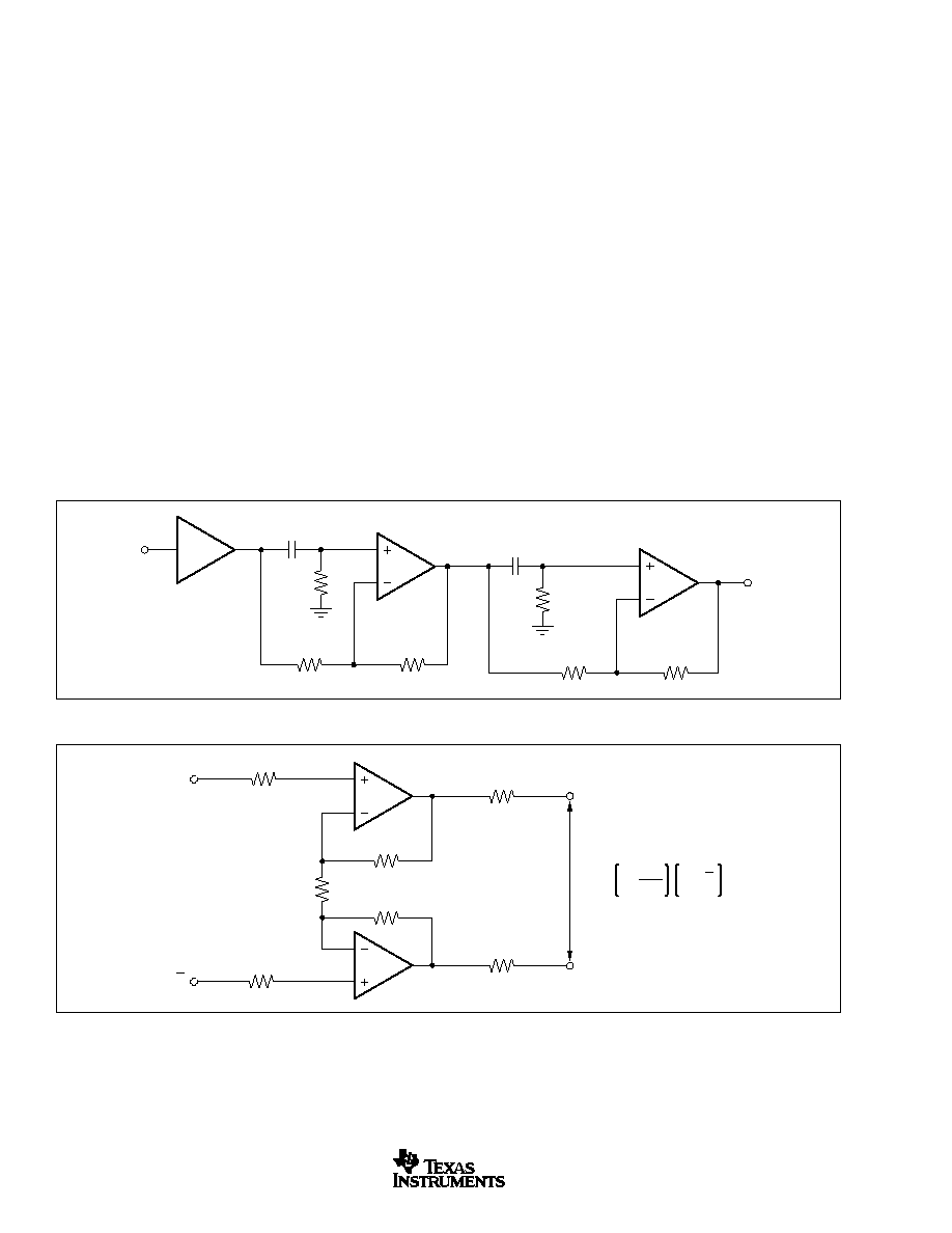
HIGH-PERFORMANCE DAC TRANSIMPEDANCE
AMPLIFIER
High-frequency DDS Digital-to-Analog Converters (DACs)
require a low distortion output amplifier to retain their SFDR
performance into real-world loads. See Figure 5 for a differ-
ential output drive implementation. The diagram shows the
signal output current(s) connected into the virtual ground
summing junction(s) of the OPA2690, which is set up as a
transimpedance stage or I-V converter. If the DAC requires
its outputs terminated to a compliance voltage other than
ground for operation, the appropriate voltage level may be
applied to the noninverting inputs of the OPA2690. The DC
gain for this circuit is equal to R
F
. At high frequencies, the
DAC output capacitance (C
D
in Figure 5) will produce a zero
FIGURE 4. SFDR vs I
B
.
FIGURE 3. Single-Supply ADC Input Driver. One of two channels.
1/2
OPA2690
402
50
402
59
1V
PP
698
698
V
I
+5V
0.1
µ
F
R
S
30
I
B
R
B
50pF
0.1
µ
F
2.5V DC
±
1V AC
ADC Input
Power-supply decoupling not shown.
70
68
66
64
62
60
58
56
54
52
50
Output Pull-Down Current (mA)
0
1
2
3
4
5
6
7
8
9
10
SFDR (dBc)
V
O
= 2V
PP
, 10MHz

OPA2690
15
SBOS238B
www.ti.com
in the noise gain for the OPA2690 that may cause peaking
in the closed-loop frequency response. C
F
is added across
R
F
to compensate for this noise gain peaking. To achieve a
flat transimpedance frequency response, the pole in each
feedback network should be set to:
1 2
4
/
/
R C
GBP
R C
F
F
F
D
=
(1)
which will give a cutoff frequency f
≠3dB
of approximately:
f
GBP
R C
dB
F
D
-
=
3
2
/
(2)
WIDEBAND VIDEO MULTIPLEXING
One common application for video speed amplifiers that
include a disable pin is to wire multiple amplifier outputs
together, then select which one of several possible video
inputs to source onto a single line. This simple wired-OR
video multiplexer can be easily implemented using the
OP2690I-14D (SO-14 package only), as shown in Figure 6.
Typically, channel switching is performed either on sync or
retrace time in the video signal. The two inputs are approxi-
mately equal at this time. The make-before-break disable
characteristic of the OPA2690 ensures that there is always
one amplifier controlling the line when using a wired-OR circuit
like that shown in Figure 6. As both inputs may be on for a
short period during the transition between channels, the out-
puts are combined through the output impedance matching
resistors (82.5
in this case). When one channel is disabled,
its feedback network forms part of the output impedance and
slightly attenuates the signal in getting out onto the cable. The
gain and output matching resistor have been slightly increased
to get a signal gain of +1 at the matched load and provide a
75
output impedance to the cable. The video multiplexer
connection (as shown in Figure 6) also ensures that the
maximum differential voltage across the inputs of the unselected
channel does not exceed the rated
±
1.2V maximum for
standard video signal levels.
See the Disable Operation section for the turn-on and turn-
off switching glitches using a 0V input for a single channel is
typically less than
±
50mV. Where two outputs are switched
(as shown in Figure 6), the output line is always under the
control of one amplifier or the other due to the make-before-
break disable timing. In this case, the switching glitches for
two 0V inputs drops to < 20mV.
FIGURE 5. High-Speed DAC--Differential Transimpedance
Amplifier.
1/2
OPA2690
1/2
OPA2690
High-Speed
DAC
V
O
= I
O
R
F
V
O
= I
O
R
F
R
F1
R
F2
C
F1
C
F2
GBP
Gain Bandwidth
Product (Hz) for the OPA2690
C
D1
C
D2
I
O
I
O
50
50
FIGURE 6. 2-Channel Video Multiplexer (SO-14 package only).
146
2k
82.5
75
Cable
75
Load
RG-59
82.5
75
402
340
Video 1
+5V
+5V
≠5V
1/2
OPA2690
1/2
OPA2690
146
2k
75
402
340
Video 2
≠5V
+5V
V
DIS
DISA
DISB
OPA2690
16
SBOS238B
www.ti.com
HIGH-SPEED DELAY CIRCUIT
The OPA2690 makes an ideal amplifier for a variety of active
filter designs. Shown in Figure 7 is a circuit that uses the two
amplifiers within the dual OPA2690 to design a 2-stage
analog delay circuit. For simplicity, the circuit uses a dual-
supply (
±
5V) operation, but it can also be modified to operate
on a signal supply. The input to the first filter stage is driven
by the OPA692 wideband buffer amplifier to isolate the signal
input from the filter network.
Each of the two filter stages is a 1st-order filter with a voltage gain
of +1. The delay time through one filter is given by Equation 3.
t
GR0
= 2RC
(3)
For a more accurate analysis of the circuit, consider the
group delay for the amplifiers. For example, in the case of the
OPA2690, the group delay in the bandwidth from 1MHz to
100MHz is approximately 1.0ns. To account for this, modify
the transfer function, which now comes out to be:
t
GR
= 2 (2RC + T
D
)
(4)
with T
D
= (1/360) ∑ (d
/df) = delay of the op amp itself. The
values of resistors R
F
and R
G
should be equal and low to
avoid parasitic effects. If the all-pass filter is designed for
very low delay times, include parasitic board capacitances to
calculate the correct delay time. Simulating this application
using the PSPICE model of the OPA2690 will allow this
design to be tuned to the desired performance.
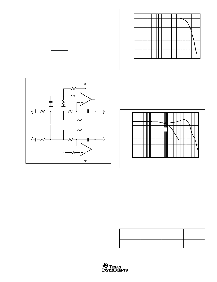
DIFFERENTIAL RECEIVER/DRIVER
A very versatile application for a dual operational amplifier is
the differential amplifier configuration shown in Figure 8. With
both amplifiers of the OPA2690 connected for noninverting
operation, the circuit provides a high input impedance whereas
the gain can easily be set by just one resistor, R
G
. When
operated in low gains, the output swing may be limited as a
result of the common-mode input swing limits of the amplifier
itself. An interesting modification of this circuit is to place a
capacitor in series with the R
G
. Now the DC gain for each
side is reduced to +1, whereas the AC gain still follows the
standard transfer function of G = 1 + 2R
F
/R
G
. This might be
advantageous for applications processing only a frequency
band that excludes DC or very low frequencies. An input DC
voltage resulting from input bias currents is not amplified by
the AC gain and can be kept low. This circuit can be used as
a differential line receiver, driver, or as an interface to a
differential input ADC.
FIGURE 7. 2-Stage, All-Pass Network.
R
R
F
402
R
G
402
R
F
402
R
G
402
V
IN
V
OUT
R
1/2
OPA2690
OPA692
C
C
1/2
OPA2690
FIGURE 8. High-Speed Differential Receiver.
50
V
I
V
I
R
O
R
O
R
F
402
R
F
402
50
R
G
1/2
OPA2690
1/2
OPA2690
V
DIFF
= 1 +
V
I
≠ V
I
2R
F
R
G
OPA2690
17
SBOS238B
www.ti.com
SINGLE-SUPPLY MFB DIFFERENTIAL ACTIVE FILTER:
10MHz BUTTERWORTH CONFIGURATION
The active filter circuit shown in Figure 9 can be easily
implemented using the OPA2690. In this configuration, each
amplifier of the OPA2690 operates as an integrator. For this
reason, this type of application is also called infinite gain filter
implementation. A Butterworth filter can be implemented
using the following component ratios.
=
=
=
=
=
=
∑
∑
∑
∑
∑
∑
O
R C
cutoff frequency
R
R
R
R
R
C
C
C
C
1
2
0 65
0 375
2
1
2
3
1
2
(
)
.
.
FIGURE 9. Single-Supply, MFB Active Filter. 10MHz LP Butterworth.
The frequency response for a 10MHz Butterworth filter is
shown in Figure 10. One advantage for using this type of filter
is the independent setting of W
O
and Q. Q can be easily
adjusted by changing the R
3A, B
resistors without affecting W
O
.
SINGLE-SUPPLY DIFFERENTIAL ADC DRIVER
The single-supply differential ADC driver shown on the front
page is ideal for driving high-frequency ADCs. As shown in
the plot on the front page, "Harmonic Distortion vs Frequency
for the Single-Supply Differential ADC Driver," the 2nd-
harmonic reacts as expected and drops to a ≠95dBc at 1MHz
and ≠87dBc at 5MHz--a significant improvement in going to
differential from single-ended.
FIGURE 10. Multiple Feedback Filter Frequency Response.
BOARD
PART
ORDERING
PRODUCT
PACKAGE
NUMBER
NUMBER
OPA2690ID
SO-8
DEM-OPA268xU
SBOU003
OPA2690I-14D
SO-14
DEM-OPA268xN
SBOU002
FIGURE 11. Single-Supply Differential ADC Driver.
Differential Gain (dB)
Frequency (MHz)
9
6
3
0
≠3
≠6
≠9
≠12
0.1
10
1
500
100
C
F
= 8.6pF
For example, C
F
= 8.6pF in parallel with R
F
= 402
will
control the ≠3dB frequency to 18MHz.
DESIGN-IN TOOLS
DEMONSTRATION BOARDS
Several PC boards are available to assist in the initial evalu-
ation of circuit performance using the OPA2690 in its two
package styles. All of these are available free as an unpopulated
PC board delivered with descriptive documentation. The sum-
mary information for these boards is shown below:
6k
R
2A
102
C
1A
100pF
C
2
200pF
C
1B
100pF
R
1A
102
R
1B
102
R
3A
60
R
3B
60
50
6k
+12V
V
CM
V
CM
V
OUT
V
IN
1000pF
50
1/2
OPA2690
1/2
OPA2690
R
2B
102
Gain (dB)
Frequency (MHz)
0.1
1
10
20
1
0
≠1
≠2
≠3
≠4
≠5
≠6
≠7
≠8
≠9
Consult the Texas Instruments web site (www.ti.com) to
request any of these boards.
The circuit shown on the front page has a 195MHz, ≠3dB
bandwidth that can be easily bandlimited by using a capaci-
tor in parallel with the feedback resistors. Refer to Figure 11
for more details. The ≠3dB frequency is given by Equation 5.
f
R C
dB
F
F
≠3
1
2
=
(5)

OPA2690
18
SBOS238B
www.ti.com
MACROMODELS
Computer simulation of circuit performance using SPICE is
often useful when analyzing the performance of analog circuits
and systems. This is particularly true for Video and RF
amplifier circuits where parasitic capacitance and inductance
can have a major effect on circuit performance. A SPICE
model for the OPA2690 (use two OPA690 SPICE models) is
available through the Texas Instruments Internet web page
(http://www.ti.com). These models do a good job of predicting
small-signal AC and transient performance under a wide
variety of operating conditions. They do not do as well in
predicting the harmonic distortion or dG/dP characteristics.
These models do not attempt to distinguish between the
package types in their small-signal AC performance.
OPERATING SUGGESTIONS
OPTIMIZING RESISTOR VALUES
As the OPA2690 is a unity-gain stable voltage-feedback op
amp, a wide range of resistor values may be used for the
feedback and gain setting resistors. The primary limits on these
values are set by dynamic range (noise and distortion) and
parasitic capacitance considerations. For a noninverting unity-
gain follower application, the feedback connection should be
made with a 25
resistor, not a direct short. This will isolate the
inverting input capacitance from the output pin and improve the
frequency response flatness. Usually, the feedback resistor
value should be between 200
and 1.5k
. Below 200
, the
feedback network will present additional output loading which
can degrade the harmonic distortion performance of the
OPA2690. Above 1.5k
, the typical parasitic capacitance
(approximately 0.2pF) across the feedback resistor can cause
unintentional band-limiting in the amplifier response.
A good rule of thumb is to target the parallel combination of R
F
and R
G
(see Figure 1) to be less than approximately 300
. The
combined impedance R
F
|| R
G
interacts with the inverting input
capacitance, placing an additional pole in the feedback net-
work and thus, a zero in the forward response. Assuming a 2pF
total parasitic on the inverting node, holding R
F
|| R
G
< 300
will
keep this pole above 250MHz. By itself, this constraint implies
that the feedback resistor R
F
can increase to several k
at high
gains. This is acceptable as long as the pole formed by R
F
and
any parasitic capacitance appearing in parallel is kept out of the
frequency range of interest.
BANDWIDTH vs GAIN: NONINVERTING OPERATION
Voltage-feedback op amps exhibit decreasing closed-loop
bandwidth as the signal gain is increased. In theory, this
relationship is described by the Gain Bandwidth Product
(GBP) shown in the electrical characteristics. Ideally, dividing
GBP by the noninverting signal gain (also called the Noise
Gain, or NG) will predict the closed-loop bandwidth. In
practice, this only holds true when the phase margin ap-
proaches 90
∞
, as it does in high gain configurations. At low
gains (increased feedback factor), most amplifiers will exhibit
a more complex response with lower phase margin. The
OPA2690 is compensated to give a slightly peaked response
in a noninverting gain of 2 (see Figure 1). This results in a
typical gain of +2 bandwidth of 220MHz, far exceeding that
predicted by dividing the 300MHz GBP by 2. Increasing the
gain will cause the phase margin to approach 90
∞
and the
bandwidth to more closely approach the predicted value of
(GBP/NG). At a gain of +10, the 30MHz bandwidth shown in
the Electrical Characteristics agrees with that predicted using
the simple formula and the typical GBP of 300MHz.
The frequency response in a gain of +2 may be modified to
achieve exceptional flatness simply by increasing the noise
gain to 2.5. One way to do this, without affecting the +2 signal
gain, is to add an 804
resistor across the two inputs in the
circuit of Figure 1. A similar technique may be used to reduce
peaking in unity gain (voltage follower) applications. For
example, by using a 402
feedback resistor along with a
402
resistor across the two op amp inputs, the voltage
follower response will be similar to the gain of +2 response
of Figure 2. Reducing the value of the resistor across the op
amp inputs will further limit the frequency response due to
increased noise gain.
The OPA2690 exhibits minimal bandwidth reduction going to
single-supply (+5V) operation as compared with
±
5V. This is
because the internal bias control circuitry retains nearly
constant quiescent current as the total supply voltage be-
tween the supply pins is changed.
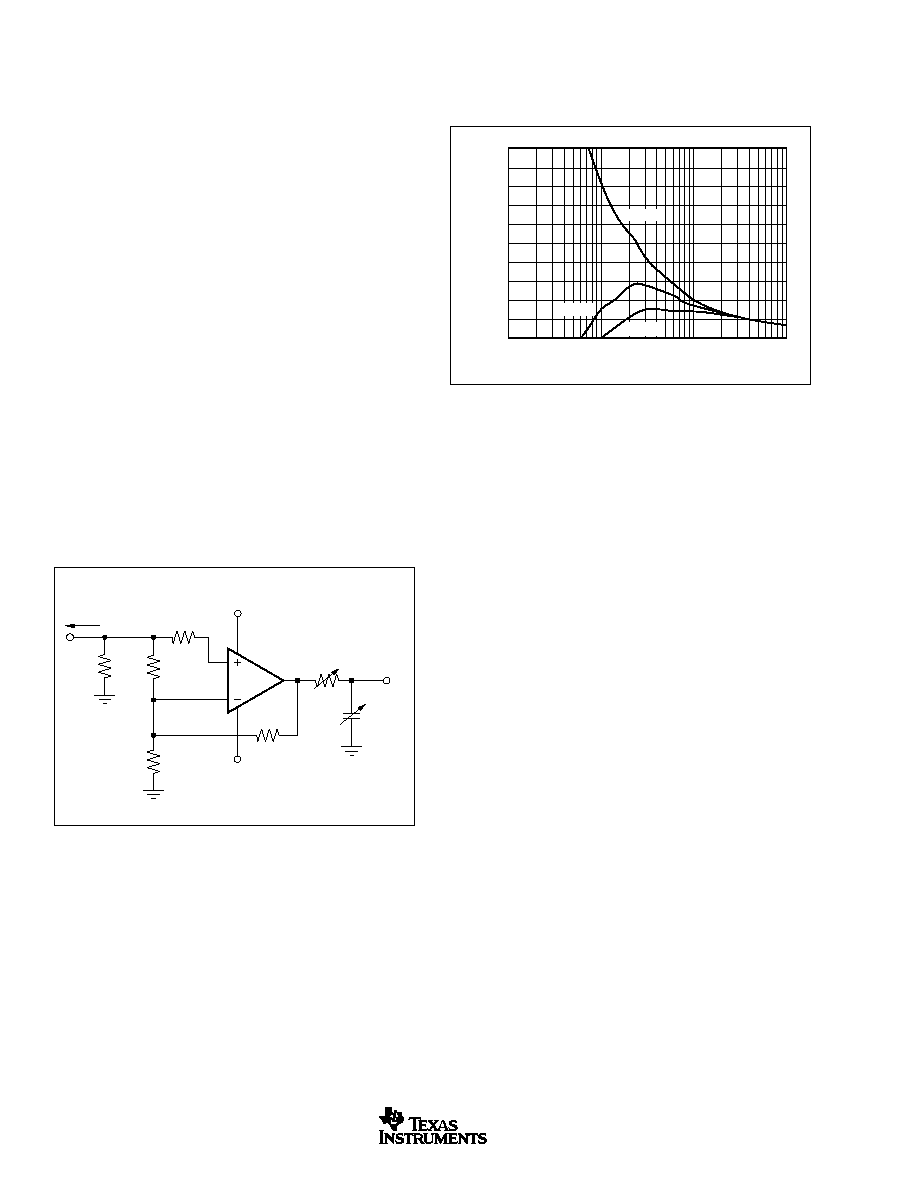
INVERTING AMPLIFIER OPERATION
As the OPA2690 is a general-purpose, wideband voltage-
feedback op amp, all of the familiar op amp application
circuits are available to the designer. Inverting operation is
one of the more common requirements and offers several
performance benefits. Figure 12 shows a typical inverting
configuration where the I/O impedances and signal gain from
Figure 1 are retained in an inverting circuit configuration.
FIGURE 12. Gain of ≠2 Example Circuit.
1/2
OPA2690
50
R
F
402
R
G
200
R
B
146
R
M
67
Source
+5V
≠5V
R
O
50
0.1
µ
F
6.8
µ
F
+
0.1
µ
F
0.1
µ
F
6.8
µ
F
+
50
Load
V
O
V
I
= ≠2
V
O
V
I

OPA2690
19
SBOS238B
www.ti.com
In the inverting configuration, three key design consider-
ations must be noted. The first is that the gain resistor (R
G
)
becomes part of the signal channel input impedance. If input
impedance matching is desired (which is beneficial when-
ever the signal is coupled through a cable, twisted pair, long
PC board trace, or other transmission line conductor), R
G
can
be set equal to the required termination value and R
F
adjusted to give the desired gain. This is the simplest
approach and results in optimum bandwidth and noise per-
formance. However, at low inverting gains, the resultant
feedback resistor value can present a significant load to the
amplifier output. For an inverting gain of ≠2, setting R
G
to
50
for input matching eliminates the need for R
M
but
requires a 100
feedback resistor. This has the interesting
advantage that the noise gain becomes equal to 2 for a 50
source impedance--the same as the noninverting circuits
considered in the previous section. The amplifier output,
however, will now see the 100
feedback resistor in parallel
with the external load. In general, the feedback resistor
should be limited to the 200
to 1.5k
range. In this case,
it is preferable to increase both the R
F
and R
G
values (see
Figure 8), and then achieve the input matching impedance
with a third resistor (R
M
) to ground. The total input impedance
becomes the parallel combination of R
G
and R
M
.
The second major consideration, touched on in the previous
paragraph, is that the signal source impedance becomes
part of the noise gain equation and influences the bandwidth.
For the example in Figure 12, the R
M
value combines in
parallel with the external 50
source impedance, yielding an
effective driving impedance of 50
|| 67
= 28.6
. This
impedance is added in series with R
G
for calculating the
noise gain (NG). The resultant NG is 2.8 for Figure 12, as
opposed to only 2 if R
M
could be eliminated as discussed
above. The bandwidth will, therefore, be slightly lower for the
gain of ≠2 circuit of Figure 12 than for the gain of +2 circuit
of Figure 1.
The third important consideration in inverting amplifier design
is setting the bias current cancellation resistor on the
noninverting input (R
B
). If this resistor is set equal to the total
DC resistance looking out of the inverting node, the output
DC error, due to the input bias currents, will be reduced to
(Input Offset Current) ∑ R
F
. If the 50
source impedance is
DC-coupled in Figure 10, the total resistance to ground on
the inverting input will be 228
. Combining this in parallel
with the feedback resistor gives the R
B
= 146
used in this
example. To reduce the additional high-frequency noise
introduced by this resistor, it is sometimes bypassed with a
capacitor. As long as R
B
< 350
, the capacitor is not required
because the total noise contribution of all other terms will be
less than that of the op amp input noise voltage. As a
minimum, the OPA2690 requires an R
B
value of 50
to damp
out parasitic-induced peaking--a direct short to ground on
the noninverting input runs the risk of a very high frequency
instability in the input stage.
OUTPUT CURRENT AND VOLTAGE
The OPA2690 provides exceptional output voltage and cur-
rent capabilities in a low-cost monolithic op amp. Under no-
load conditions at +25
∞
C, the output voltage typically swings
closer than 1V to either supply rail; the specified swing limit
is within 1.2V of either rail. Into a 15
load (the minimum
tested load), it will deliver more than
±
160mA.
The specifications described previously, though familiar in
the industry, consider voltage and current limits separately.
In many applications, it is the voltage ∑ current, or V-I product,
which is more relevant to circuit operation. Refer to the
"Output Voltage and Current Limitations" plot in the Typical
Characteristics. The X- and Y-axes of this graph shows the
zero-voltage output current limit and the zero-current output
voltage limit, respectively. The four quadrants give a more
detailed view of the OPA2690 output drive capabilities,
noting that the graph is bounded by a safe operating area of
1W maximum internal power dissipation for each channel
separately. Superimposing resistor load lines onto the plot
shows that the OPA2690 can drive
±
2.5V into 25
or
±
3.5V
into 50
without exceeding the output capabilities or the 1W
dissipation limit. A 100
load line (the standard test circuit
load) shows the full
±
3.9V output swing capability (see the
Electrical Characteristics).
The minimum specified output voltage and current specifica-
tions over temperature are set by worst-case simulations at
the cold temperature extreme. Only at cold start-up will the
output current and voltage decrease to the numbers shown
in the Electrical Characteristic tables. As the output transis-
tors deliver power, their junction temperatures increase,
decreasing their V
BE
s (increasing the available output volt-
age swing) and increasing their current gains (increasing the
available output current). In steady-state operation, the avail-
able output voltage and current is always greater than that
shown in the over-temperature specifications because the
output stage junction temperatures is higher than the mini-
mum specified operating ambient.
To protect the output stage from accidental shorts to ground
and the power supplies, output short-circuit protection is
included in the OPA2690. This circuit acts to limit the maxi-
mum source or sink current to approximately 250mA.
DRIVING CAPACITIVE LOADS
One of the most demanding and yet very common load
conditions for an op amp is capacitive loading. Often, the
capacitive load is the input of an ADC--including additional
external capacitance which may be recommended to im-
prove ADC linearity. A high-speed, high open-loop gain
amplifier like the OPA2690 can be very susceptible to de-
creased stability and closed-loop response peaking when a
capacitive load is placed directly on the output pin. When the
open-loop output resistance of the amplifier is considered,
this capacitive load introduces an additional pole in the signal
path that can decrease the phase margin. Several external
OPA2690
20
SBOS238B
www.ti.com
solutions to this problem have been suggested. When the
primary considerations are frequency response flatness, pulse
response fidelity, and/or distortion, the simplest and most
effective solution is to isolate the capacitive load from the
feedback loop by inserting a series-isolation resistor between
the amplifier output and the capacitive load. This does not
eliminate the pole from the loop response, but rather shifts it
and adds a zero at a higher frequency. The additional zero
acts to cancel the phase lag from the capacitive load pole,
thus increasing the phase margin and improving stability.
The Typical Characteristics show the recommended R
S
ver-
sus capacitive load and the resulting frequency response at
the load. Parasitic capacitive loads greater than 2pF can
begin to degrade the performance of the OPA2690. Long PC
board traces, unmatched cables, and connections to multiple
devices can easily exceed this value. Always consider this
effect carefully, and add the recommended series resistor as
close as possible to the OPA2690 output pin (see the Board
Layout Guidelines section).
The criterion for setting this R
S
resistor is a maximum
bandwidth, flat frequency response at the load. For the
OPA2690 operating in a gain of +2, the frequency response
at the output pin is already slightly peaked without the
capacitive load requiring relatively high values of R
S
to flatten
the response at the load. Increasing the noise gain will
reduce the peaking as described previously. The circuit of
Figure 13 demonstrates this technique, allowing lower values
of R
S
to be used for a given capacitive load.
margin) then sweeping C
LOAD
and finding the required R
S
to get
a flat frequency response. This plot also gives the required R
S
versus C
LOAD
for the OPA2690 operated at higher signal gains
without R
NG
.
FIGURE 13. Capacitive Load Driving with Noise Gain Tuning.
1/2
OPA2690
402
175
402
+5V
50
50
C
LOAD
R
NG
V
O
R
≠5V
Power-supply decoupling
not shown.
FIGURE 14. Required R
S
vs Noise Gain.
100
90
80
70
60
50
40
30
20
10
0
Capacitive Load (pF)
1
10
100
1000
R
S
(
)
NG = 2
NG = 3
NG = 4
This gain of +2 circuit includes a noise gain tuning resistor
across the two inputs to increase the noise gain, increasing the
unloaded phase margin for the op amp. Although this tech-
nique will reduce the required R
S
resistor for a given capacitive
load, it does increase the noise at the output. It also will
decrease the loop gain, nominally decreasing the distortion
performance. If, however, the dominant distortion mechanism
arises from a high R
S
value, significant dynamic range im-
provement can be achieved using this technique. Figure 14
shows the required R
S
versus C
LOAD
parametric on noise gain
using this technique. This is the circuit of Figure 13 with R
NG
adjusted to increase the noise gain (increasing the phase
DISTORTION PERFORMANCE
The OPA2690 provides good distortion performance into a
100
load on
±
5V supplies. Relative to alternative solutions,
it provides exceptional performance into lighter loads and/or
operating on a single +5V supply. Generally, until the funda-
mental signal reaches very high frequency or power levels,
the 2nd-harmonic dominates the distortion with a negligible
3rd-harmonic component. Focusing then on the 2nd-har-
monic, increasing the load impedance improves distortion
directly. Remember that the total load includes the feedback
network; in the noninverting configuration (see Figure 1) this
is the sum of R
F
+ R
G
, whereas in the inverting configuration
it is just R
F
. Also, providing an additional supply-decoupling
capacitor (0.1
µ
F) between the supply pins (for bipolar opera-
tion) improves the 2nd-order distortion slightly (3dB to 6dB).
Operating differentially also lowers 2nd-harmonic distortion
terms (see the plot on the front page).
In most op amps, increasing the output voltage swing in-
creases harmonic distortion directly. The new output stage
used in the OPA2690 actually holds the difference between
fundamental power and the 2nd- and 3rd-harmonic powers
relatively constant with increasing output power until very large
output swings are required (> 4V
PP
). This also shows up in the
2-tone, 3rd-order intermodulation spurious (IM3) response
curves. The 3rd-order spurious levels are extremely low at low
output power levels. The output stage continues to hold them
low even as the fundamental power reaches very high levels.
As the Typical Characteristics show, the spurious
intermodulation powers do not increase as predicted by a
traditional intercept model. As the fundamental power level
increases, the dynamic range does not decrease significantly.
For 2 tones centered at 20MHz, with 10dBm/tone into a
matched 50
load (i.e., 2V
PP
for each tone at the load, which
requires 8V
PP
for the overall 2-tone envelope at the output
pin), the Typical Characteristics show 46dBc difference
OPA2690
21
SBOS238B
www.ti.com
between the test tone powers and the 3rd-order intermodulation
spurious powers. This exceptional performance improves fur-
ther when operating at lower frequencies or powers.
NOISE PERFORMANCE
High slew rate, unity-gain stable, voltage-feedback op amps
usually achieve their slew rate at the expense of a higher
input noise voltage. The 5.5nV/
Hz input voltage noise for
the OPA2690 is, however, much lower than comparable
amplifiers. The input-referred voltage noise, and the two
input-referred current noise terms, combine to give low
output noise under a wide variety of operating conditions.
Figure 15 shows the op amp noise analysis model with all the
noise terms included. In this model, all noise terms are taken
to be noise voltage or current density terms in either nV/
Hz
or pA/
Hz.
flatness considerations. As the resistor-induced noise is rela-
tively negligible, additional capacitive decoupling across the
bias current cancellation resistor (R
B
) for the inverting op amp
configuration of Figure 12 is not required.
DC ACCURACY AND OFFSET CONTROL
The balanced input stage of a wideband voltage-feedback op
amp allows good output DC accuracy in a wide variety of
applications. The power-supply current trim for the OPA2690
gives even tighter control than comparable amplifiers. Al-
though the high-speed input stage does require relatively
high input bias current (typically 5
µ
A out of each input
terminal), the close matching between them may be used to
reduce the output DC error caused by this current. The total
output offset voltage may be considerably reduced by match-
ing the DC source resistances appearing at the two inputs.
This reduces the output DC error due to the input bias
currents to the offset current times the feedback resistor.
Evaluating the configuration of Figure 1, and using worst-
case +25
∞
C input offset voltage and current specifications,
gives a worst-case output offset voltage equal to:
±
(NG ∑ V
OS(MAX)
)
±
(R
F
∑ I
OS(MAX)
)
=
±
(2 ∑ 4.5mV)
±
(402
∑ 1
µ
A)
=
±
9.4mV ≠ (NG = noninverting signal gain)
A fine-scale output offset null, or DC operating point adjust-
ment, is often required. Numerous techniques are available
for introducing DC offset control into an op amp circuit. Most
of these techniques eventually reduce to adding a DC current
through the feedback resistor. In selecting an offset trim
method, one key consideration is the impact on the desired
signal path frequency response. If the signal path is intended
to be noninverting, the offset control is best applied as an
inverting summing signal to avoid interaction with the signal
source. If the signal path is intended to be inverting, applying
the offset control to the noninverting input can be considered.
However, the DC offset voltage on the summing junction sets
up a DC current back into the source that must be consid-
ered. Applying an offset adjustment to the inverting op amp
input can change the noise gain and frequency response
flatness. For a DC-coupled inverting amplifier, see Figure 16
for one example of an offset adjustment technique that has
minimal impact on the signal frequency response. In this
case, the DC offsetting current is brought into the inverting
input node through resistor values that are much larger than
the signal path resistors. This ensures that the adjustment
circuit has minimal effect on the loop gain and hence, the
frequency response.
DISABLE OPERATION (SO-14 Package Only)
The OPA2690I-14D provides an optional disable feature that
can be used either to reduce system power or to implement a
simple channel multiplexing operation. If the DIS control pin is
left unconnected, the OPA2690I-14D will operate normally. To
disable, the control pin must be asserted LOW. See Figure 17
for a simplified internal circuit for the disable control feature.
FIGURE 15. Op Amp Noise Analysis Model.
4kT
R
G
R
G
R
F
R
S
1/2
OPA2690
I
BI
E
O
I
BN
4kT = 1.6E ≠ 20J
at 290
∞
K
E
RS
E
NI
4kTR
S
4kTR
F
The total output spot noise voltage can be computed as the
square root of the sum of all squared output noise voltage
contributors. Equation 6 shows the general form for the
output noise voltage using the terms shown in Figure 15.
E
E
I
R
kTR
NG
I R
kTR NG
O
NI
BN
S
S
BI
F
F
=
+
(
)
+
+
(
)
+
2
2
2
2
4
4
(6)
Dividing this expression by the noise gain (NG = (1 + R
F
/R
G
))
will give the equivalent input-referred spot noise voltage at
the noninverting input, as shown in Equation 7.
E
E
I
R
kTR
I R
NG
kTR
NG
N
NI
BN
S
S
BI
F
F
=
+
(
)
+
+
+
2
2
2
4
4
(7)
Evaluating these two equations for the OPA2690 circuit and
component values, see Figure 1, gives a total output spot
noise voltage of 12.3nV/
Hz and a total equivalent input spot
noise voltage of 6.1nV/
Hz. This is including the noise added
by the bias current cancellation resistor (175
) on the
noninverting input. This total input-referred spot noise voltage
is only slightly higher than the 5.5nV/
Hz specification for the
op amp voltage noise alone. This is the case as long as the
impedances appearing at each op amp input are limited to the
previously recommend maximum value of 300
. Keeping both
(R
F
|| R
G
) and the noninverting input source impedance less
than 300
will satisfy both noise and frequency response
OPA2690
22
SBOS238B
www.ti.com
In normal operation, base current to Q1 is provided through
the 110k
resistor, while the emitter current through the
15k
resistor sets up a voltage drop that is inadequate to
turn on the two diodes in Q1's emitter. As V
DIS
is pulled LOW,
additional current is pulled through the 15k
resistor eventu-
ally turning on those two diodes (
100
µ
A). At this point, any
further current pulled out of V
DIS
goes through those diodes
holding the emitter-base voltage of Q1 at approximately 0V.
This shuts off the collector current out of Q1, turning the
amplifier off. The supply current in the disable mode are only
those required to operate the circuit of Figure 16. Additional
circuitry ensures that turn-on time occurs faster than turn-off
time (make-before-break).
When disabled, the output and input nodes go to a high-
impedance state. If the OPA2690 is operating in a gain of +1,
this will show a very high impedance at the output and excep-
tional signal isolation. If operating at a gain greater than +1, the
total feedback network resistance (R
F
+ R
G
) will appear as the
impedance looking back into the output, but the circuit will still
show very high forward and reverse isolation. If configured as
an inverting amplifier, the input and output will be connected
through the feedback network resistance (R
F
+ R
G
) and the
isolation will be very poor as a result.
One key parameter in disable operation is the output glitch
when switching in and out of the disabled mode. Figure 18
shows these glitches for the circuit of Figure 1 with the input
signal at 0V. The glitch waveform at the output pin is plotted
along with the DIS pin voltage.
FIGURE 16. DC-Coupled, Inverting Gain of ≠2, with Offset
Adjustment.
R
F
1k
±
200mV Output Adjustment
= ≠ = ≠2
Power-supply
decoupling not shown.
5k
5k
328
0.1
µ
F
R
G
500
V
I
20k
10k
0.1
µ
F
≠5V
+5V
1/2
OPA2690
+5V
≠5V
V
O
V
O
V
I
R
F
R
G
FIGURE 17. Simplified Disable Control Circuit.
25k
110k
15k
I
S
Control
≠V
S
+V
S
V
DIS
Q1
FIGURE 18. Disable/Enable Glitch.
Time (20ns/div)
Output V
oltage (10mV/div)
30
20
10
0
≠10
≠20
≠30
V
DIS
(2V/div)
6
4
2
0
V
O
= 0
V
DIS
Output Voltage
The transition edge rate (dv/dt) of the DIS control line
influences this glitch. For the plot of Figure 18, the edge rate
was reduced until no further reduction in glitch amplitude was
observed. This approximately 1V/ns maximum slew rate can
be achieved by adding a simple RC filter into the DIS pin
from a higher speed logic line. If extremely fast transition
logic is used, a 2k
series resistor between the logic gate
and the DIS input pin provides adequate bandlimiting using
just the parasitic input capacitance on the DIS pin while still
ensuring adequate logic level swing.
THERMAL ANALYSIS
Due to the high output power capability of the OPA2690,
heatsinking or forced airflow may be required under extreme
operating conditions. Maximum desired junction temperature
will set the maximum allowed internal power dissipation as
described following. In no case should the maximum junction
temperature be allowed to exceed 150
∞
C.
Operating junction temperature (T
J
) is given by T
A
+ P
D
∑
JA
.
The total internal power dissipation (P
D
) is the sum of
quiescent power (P
DQ
) and additional power dissipated in the
output stage (P
DL
) to deliver load power. Quiescent power is
simply the specified no-load supply current times the total
supply voltage across the part. P
DL
depends on the required
output signal and load but, for a grounded resistive load, be
at a maximum when the output is fixed at a voltage equal to
1/2 of either supply voltage (for equal bipolar supplies).
Under this condition, P
DL
= V
S
2
/(4 ∑ R
L
), where R
L
includes
feedback network loading.

OPA2690
23
SBOS238B
www.ti.com
Note that it is the power in the output stage and not into the
load that determines internal power dissipation.
As a worst-case example, compute the maximum T
J
using an
OPA2690ID (SO-8 package) in the circuit of Figure 1 operat-
ing at the maximum specified ambient temperature of +85
∞
C
and with both outputs driving a grounded 20
load to +2.5V.
P
D
= 10V ∑ 12.6mA + 2 [5
2
/(4 ∑ (20
|| 804
))] = 766mW
Maximum T
J
= +85
∞
C + (0.766W ∑ 125
∞
C/W) = 180
∞
C.
This absolute worst-case condition exceeds the specified
maximum junction temperature. Actual P
DL
is normally less
than that considered here. Carefully consider maximum T
J
in
your application.
BOARD LAYOUT GUIDELINES
Achieving optimum performance with a high-frequency am-
plifier like the OPA2690 requires careful attention to board
layout parasitics and external component types. Recommen-
dations that will optimize performance include:
a) Minimize parasitic capacitance to any AC ground for all
of the signal I/O pins. Parasitic capacitance on the output and
inverting input pins can cause instability: on the noninverting
input, it can react with the source impedance to cause
unintentional bandlimiting. To reduce unwanted capacitance,
a window around the signal I/O pins should be opened in all
of the ground and power planes around those pins. Other-
wise, ground and power planes should be unbroken else-
where on the board.
b) Minimize the distance (< 0.25") from the power-supply
pins to high frequency 0.1
µ
F decoupling capacitors. At the
device pins, the ground and power-plane layout should not
be in close proximity to the signal I/O pins. Avoid narrow
power and ground traces to minimize inductance between
the pins and the decoupling capacitors. The power-supply
connections should always be decoupled with these capaci-
tors. An optional supply decoupling capacitor (0.1
µ
F) across
the two power supplies (for bipolar operation) will improve
2nd-harmonic distortion performance. Larger (2.2
µ
F to 6.8
µ
F)
decoupling capacitors, effective at lower frequencies, should
also be used on the main supply pins. These may be placed
somewhat farther from the device and may be shared among
several devices in the same area of the PC board.
c) Careful selection and placement of external compo-
nents will preserve the high-frequency performance of the
OPA2690. Resistors should be a very low reactance type.
Surface-mount resistors work best and allow a tighter overall
layout. Metal film or carbon composition axially-leaded resis-
tors can also provide good high-frequency performance. Again,
keep their leads and PC board traces as short as possible.
Never use wirewound type resistors in a high-frequency appli-
cation. Since the output pin and inverting input pin are the
most sensitive to parasitic capacitance, always position the
feedback and series output resistor, if any, as close as
possible to the output pin. Other network components, such as
noninverting input termination resistors, should also be placed
close to the package. Even with a low parasitic capacitance
shunting the external resistors, excessively high resistor val-
ues can create significant time constants that can degrade
performance. Good axial metal film or surface-mount resistors
have approximately 0.2pF in shunt with the resistor. For
resistor values > 1.5k
, this parasitic capacitance can add a
pole and/or zero below 500MHz that can effect circuit opera-
tion. Keep resistor values as low as possible consistent with
load driving considerations. The 402
feedback used in the
Electrical Characteristics is a good starting point for design.
Note that a 25
feedback resistor, rather than a direct short,
is suggested for the unity-gain follower application. This effec-
tively isolates the inverting input capacitance from the output
pin that would otherwise cause additional peaking in the gain
of +1 frequency response.
d) Connections to other wideband devices on the board
may be made with short direct traces or through onboard
transmission lines. For short connections, consider the trace
and the input to the next device as a lumped capacitive load.
Relatively wide traces (50mils to 100mils) should be used,
preferably with ground and power planes opened up around
them. Estimate the total capacitive load and set R
S
from the
plot of "Recommended R
S
vs Capacitive Load." Low parasitic
capacitive loads (< 3pF) may not need an R
S
because the
OPA2690 is nominally compensated to operate with a 2pF
parasitic load. Higher parasitic capacitive loads without an R
S
are allowed as the signal gain increases (increasing the
unloaded phase margin, see Figure 14). If a long trace is
required, and the 6dB signal loss intrinsic to a doubly-
terminated transmission line is acceptable, implement a
matched impedance transmission line using microstrip or
stripline techniques (consult an ECL design handbook for
microstrip and stripline layout techniques). A 50
environ-
ment is normally not necessary on board, and in fact, a
higher impedance environment will improve distortion as
shown in the distortion versus load plots. With a characteris-
tic board trace impedance defined (based on board material
and trace dimensions), a matching series resistor into the
trace from the output of the OPA2690 is used as well as a
terminating shunt resistor at the input of the destination
device. Remember also that the terminating impedance will
be the parallel combination of the shunt resistor and the input
impedance of the destination device; this total effective
impedance should be set to match the trace impedance. The
high output voltage and current capability of the OPA2690
allows multiple destination devices to be handled as sepa-
rate transmission lines, each with their own series and shunt
terminations. If the 6dB attenuation of a doubly-terminated
transmission line is unacceptable, a long trace can be series-
terminated at the source end only. Treat the trace as a
capacitive load in this case and set the series resistor value
as shown in the plot of "Recommended R
S
vs Capacitive
Load." This will not preserve signal integrity as well as a
doubly-terminated line. If the input impedance of the destina-
tion device is low, there will be some signal attenuation due
to the voltage divider formed by the series output into the
terminating impedance.
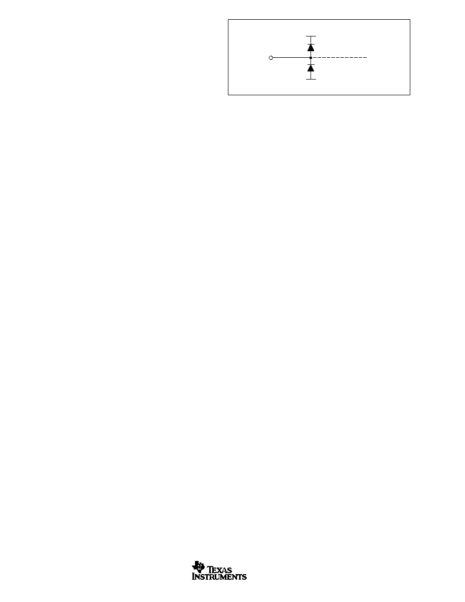
OPA2690
24
SBOS238B
www.ti.com
FIGURE 19. Internal ESD Protection.
External
Pin
+V
CC
≠V
CC
Internal
Circuitry
e) Socketing a high-speed part like the OPA2690 is not
recommended. The additional lead length and pin-to-pin
capacitance introduced by the socket can create an ex-
tremely troublesome parasitic network which can make it
almost impossible to achieve a smooth, stable frequency
response. Best results are obtained by soldering the OPA2690
onto the board.
INPUT AND ESD PROTECTION
The OPA2690 is built using a very high-speed complemen-
tary bipolar process. The internal junction breakdown volt-
ages are relatively low for these very small geometry de-
vices. These breakdowns are reflected in the Absolute Maxi-
mum Ratings table. All device pins are protected with internal
ESD protection diodes to the power supplies, as shown in
Figure 19.
These diodes provide moderate protection to input overdrive
voltages above the supplies as well. The protection diodes
can typically support 30mA continuous current. Where higher
currents are possible (e.g., in systems with
±
15V supply parts
driving into the OPA2690), current-limiting series resistors
should be added into the two inputs. Keep these resistor
values as low as possible since high values degrade both
noise performance and frequency response.
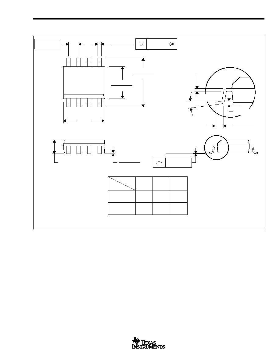
OPA2690
25
SBOS238B
www.ti.com
PACKAGE DRAWING
D (R-PDSO-G**)
PLASTIC SMALL-OUTLINE PACKAGE
8 PINS SHOWN
8
0.197
(5,00)
A MAX
A MIN
(4,80)
0.189
0.337
(8,55)
(8,75)
0.344
14
0.386
(9,80)
(10,00)
0.394
16
DIM
PINS **
4040047/E 09/01
0.069 (1,75) MAX
Seating Plane
0.004 (0,10)
0.010 (0,25)
0.010 (0,25)
0.016 (0,40)
0.044 (1,12)
0.244 (6,20)
0.228 (5,80)
0.020 (0,51)
0.014 (0,35)
1
4
8
5
0.150 (3,81)
0.157 (4,00)
0.008 (0,20) NOM
0
∞
≠ 8
∞
Gage Plane
A
0.004 (0,10)
0.010 (0,25)
0.050 (1,27)
NOTES: A. All linear dimensions are in inches (millimeters).
B. This drawing is subject to change without notice.
C. Body dimensions do not include mold flash or protrusion, not to exceed 0.006 (0,15).
D. Falls within JEDEC MS-012

PACKAGING INFORMATION
ORDERABLE DEVICE
STATUS(1)
PACKAGE TYPE
PACKAGE DRAWING
PINS
PACKAGE QTY
OPA2690I-14D
ACTIVE
SOIC
D
14
58
OPA2690I-14DR
ACTIVE
SOIC
D
14
2500
OPA2690ID
ACTIVE
SOIC
D
8
100
OPA2690IDR
ACTIVE
SOIC
D
8
2500
(1) The marketing status values are defined as follows:
ACTIVE: Product device recommended for new designs.
LIFEBUY: TI has announced that the device will be discontinued, and a lifetime-buy period is in effect.
NRND: Not recommended for new designs. Device is in production to support existing customers, but TI does not recommend using this part in
a new design.
PREVIEW: Device has been announced but is not in production. Samples may or may not be available.
OBSOLETE: TI has discontinued the production of the device.
PACKAGE OPTION ADDENDUM
www.ti.com
3-Oct-2003

IMPORTANT NOTICE
Texas Instruments Incorporated and its subsidiaries (TI) reserve the right to make corrections, modifications,
enhancements, improvements, and other changes to its products and services at any time and to discontinue
any product or service without notice. Customers should obtain the latest relevant information before placing
orders and should verify that such information is current and complete. All products are sold subject to TI's terms
and conditions of sale supplied at the time of order acknowledgment.
TI warrants performance of its hardware products to the specifications applicable at the time of sale in
accordance with TI's standard warranty. Testing and other quality control techniques are used to the extent TI
deems necessary to support this warranty. Except where mandated by government requirements, testing of all
parameters of each product is not necessarily performed.
TI assumes no liability for applications assistance or customer product design. Customers are responsible for
their products and applications using TI components. To minimize the risks associated with customer products
and applications, customers should provide adequate design and operating safeguards.
TI does not warrant or represent that any license, either express or implied, is granted under any TI patent right,
copyright, mask work right, or other TI intellectual property right relating to any combination, machine, or process
in which TI products or services are used. Information published by TI regarding third-party products or services
does not constitute a license from TI to use such products or services or a warranty or endorsement thereof.
Use of such information may require a license from a third party under the patents or other intellectual property
of the third party, or a license from TI under the patents or other intellectual property of TI.
Reproduction of information in TI data books or data sheets is permissible only if reproduction is without
alteration and is accompanied by all associated warranties, conditions, limitations, and notices. Reproduction
of this information with alteration is an unfair and deceptive business practice. TI is not responsible or liable for
such altered documentation.
Resale of TI products or services with statements different from or beyond the parameters stated by TI for that
product or service voids all express and any implied warranties for the associated TI product or service and
is an unfair and deceptive business practice. TI is not responsible or liable for any such statements.
Following are URLs where you can obtain information on other Texas Instruments products and application
solutions:
Products
Applications
Amplifiers
amplifier.ti.com
Audio
www.ti.com/audio
Data Converters
dataconverter.ti.com
Automotive
www.ti.com/automotive
DSP
dsp.ti.com
Broadband
www.ti.com/broadband
Interface
interface.ti.com
Digital Control
www.ti.com/digitalcontrol
Logic
logic.ti.com
Military
www.ti.com/military
Power Mgmt
power.ti.com
Optical Networking
www.ti.com/opticalnetwork
Microcontrollers
microcontroller.ti.com
Security
www.ti.com/security
Telephony
www.ti.com/telephony
Video & Imaging
www.ti.com/video
Wireless
www.ti.com/wireless
Mailing Address:
Texas Instruments
Post Office Box 655303 Dallas, Texas 75265
Copyright
2003, Texas Instruments Incorporated