1MHz, 45
µ
A, CMOS, Rail-to-Rail
OPERATIONAL AMPLIFIERS
FEATURES
q
LOW I
Q
: 45
µ
A typical
q
LOW COST
q
RAIL-TO-RAIL INPUT AND OUTPUT
q
SINGLE SUPPLY: +2.1V to +5.5V
q
INPUT BIAS CURRENT:
0.5pA
q
Micro
SIZE PACKAGES:
SC70-5, SOT23-8 and
TSSOP-14
q
HIGH SPEED:POWER WITH BANDWIDTH: 1MHz
APPLICATIONS
q
PORTABLE EQUIPMENT
q
BATTERY-POWERED EQUIPMENT
q
SMOKE ALARMS
q
CO DETECTORS
q
MEDICAL INSTRUMENTATION
DESCRIPTION
The OPA348 series amplifiers are single supply, low-power,
CMOS op amps in micro packaging. Featuring an extended
bandwidth of 1MHz, and a supply current of 45
µ
A, the
OPA348 series is useful for low-power applications on single
supplies of 2.1V to 5.5V.
Low supply current of 45
µ
A, and an input bias current of
0.5pA, make the OPA348 series an optimal candidate for
low-power, high-impedance applications such as smoke de-
tectors and other sensors.
The OPA348 is available in the miniature SC70-5,
SOT23-5 and SO-8 packages. The OPA2348 is available in
SOT23-8 and SO-8 packages, and the OPA4348 is offered
in space-saving TSSOP-14 and SO-14 packages. The ex-
tended temperature range of ≠40
∞
C to +125
∞
C over all supply
voltages offers additional design flexibility.
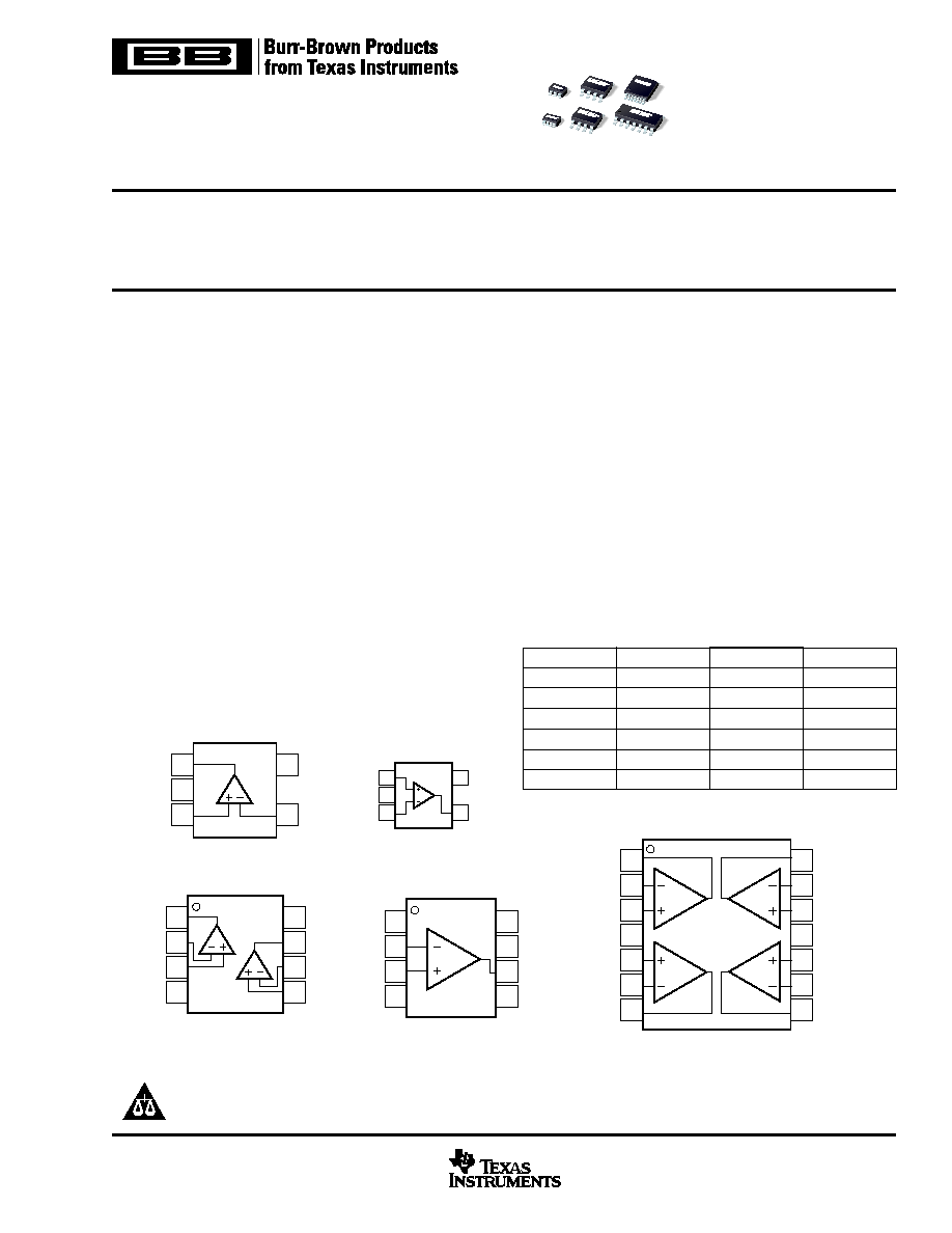
OPA348
OPA2348
OPA4348
SBOS213C ≠ NOVEMBER 2001 ≠ REVISED MAY 2002
www.ti.com
PRODUCTION DATA information is current as of publication date.
Products conform to specifications per the terms of Texas Instruments
standard warranty. Production processing does not necessarily include
testing of all parameters.
Copyright © 2001, Texas Instruments Incorporated
Please be aware that an important notice concerning availability, standard warranty, and use in critical applications of
Texas Instruments semiconductor products and disclaimers thereto appears at the end of this data sheet.
Æ
OPA348
OPA3
48
OPA2
348
OPA4
348
PACKAGES
OPA348
OPA2348
OPA4348
SOT23-5
X
SOT23-8
X
SO-8
X
X
TSSOP-14
X
SO-14
X
SC70-5
X
1
2
3
5
4
V+
≠In
Out
V≠
+In
OPA348
SOT23-5
1
2
3
4
8
7
6
5
NC
V+
Out
NC
NC
≠In
+In
V≠
OPA348
SO-8
1
2
3
4
8
7
6
5
V+
Out B
≠In B
+In B
Out A
≠In A
+In A
V≠
OPA2348
SOT23-8, SO-8
A
B
1
2
3
4
5
6
7
14
13
12
11
10
9
8
Out D
≠In D
+In D
V≠
+In C
≠In C
Out C
Out A
≠In A
+In A
V+
+In B
≠In B
Out B
OPA4348
TSSOP-14, SO-14
A
D
B
C
1
2
3
5
4
V+
Out
+In
V≠
≠In
OPA348
SC70-5

OPA348, 2348, 4348
2
SBOS213C
www.ti.com
Supply Voltage, V≠ to V+ ................................................................... 7.5V
Signal Input Terminals, Voltage
(2)
.................. (V≠) ≠ 0.5V to (V+) + 0.5V
Current
(2)
.................................................... 10mA
Output Short-Circuit
(3)
.............................................................. Continuous
Operating Temperature .................................................. ≠65
∞
C to +150
∞
C
Storage Temperature ..................................................... ≠65
∞
C to +150
∞
C
Junction Temperature ...................................................................... 150
∞
C
Lead Temperature (soldering, 10s) ................................................. 300
∞
C
NOTES: (1) Stresses above these ratings may cause permanent damage.
Exposure to absolute maximum conditions for extended periods may
degrade device reliability. These are stress ratings only. Functional opera-
tion of the device at these conditions, or beyond the specified operating
conditions, is not implied. (2) Input terminals are diode-clamped to the
power-supply rails. Input signals that can swing more than 0.5V beyond the
supply rails should be current-limited to 10mA or less. (3) Short-circuit to
ground, one amplifier per package.
ABSOLUTE MAXIMUM RATINGS
(1)
ELECTROSTATIC
DISCHARGE SENSITIVITY
This integrated circuit can be damaged by ESD. Texas Instru-
ments recommends that all integrated circuits be handled with
appropriate precautions. Failure to observe proper handling
and installation procedures can cause damage.
ESD damage can range from subtle performance degrada-
tion to complete device failure. Precision integrated circuits
may be more susceptible to damage because very small
parametric changes could cause the device not to meet its
published specifications.
PACKAGE/ORDERING INFORMATION
SPECIFIED
PACKAGE
TEMPERATURE
PACKAGE
ORDERING
TRANSPORT
PRODUCT
PACKAGE-LEAD
DESIGNATOR
(1)
RANGE
MARKING
NUMBER
(2)
MEDIA, QUANTITY
Single
OPA348AI
SOT23-5
DBV
≠40
∞
C to +125
∞
C
A48
OPA348AIDBVT
Tape and Reel, 250
"
"
"
"
"
OPA348AIDBVR
Tape and Reel, 3000
OPA348AI
SO-8
D
≠40
∞
C to +125
∞
C
348A
OPA348AID
Tubes, 100
"
"
"
"
"
OPA348AIDR
Tape and Reel, 2500
OPA348AI
SC70-5
DCK
≠40
∞
C to 125
∞
C
S48
OPA348AIDCKT
Tape and Reel, 250
"
"
"
"
"
OPA348AIDCKR
Tape and Reel, 3000
Dual
OPA2348AI
SOT23-8
DCN
≠40
∞
C to +125
∞
C
B48
OPA2348AIDCNT
Tape and Reel, 250
"
"
"
"
"
OPA2348AIDCNR
Tape and Reel, 3000
OPA2348AI
SO-8
D
≠40
∞
C to +125
∞
C
2348A
OPA2348AID
Tubes, 100
"
"
"
"
"
OPA2348AIDR
Tape and Reel, 2500
Quad
OPA4348AI
SO-14
D
≠40
∞
C to +125
∞
C
OPA4348
OPA4348AID
Tubes, 58
"
"
"
"
"
OPA4348AIDR
Tape and Reel, 2500
OPA4348AI
TSSOP-14
PW
≠40
∞
C to +125
∞
C
4348A
OPA4348AIPWT
Tubes, 250
"
"
"
"
"
OPA4348AIPWR
Tape and Reel, 2500
NOTES: (1) For the most current specifications and package information, refer to our web site at www.ti.com. (2) Models labeled with "T" indicate smaller quantity
tape and reel, "R" indicates large quantity tape and reel and "D" indicates tubes of specified quantity.

OPA348, 2348, 4348
3
SBOS213C
www.ti.com
OPA348
OPA2348
OPA4348
ELECTRICAL CHARACTERISTICS: V
S
= 2.5V to 5.5V
Boldface limits apply over the specified temperature range, T
A
= ≠40
∞
C to +125
∞
C
At T
A
= +25
∞
C, R
L
= 100k
connected to V
S
/ 2 and V
OUT
= V
S
/ 2, unless otherwise noted.
PARAMETER
CONDITION
MIN
TYP
MAX
UNITS
OFFSET VOLTAGE
Input Offset Voltage
V
OS
V
S
= 5V, V
CM
= (V≠) + 0.8V
1
5
mV
Over Temperature
6
mV
Drift
dV
OS
/dT
4
µ
V/
∞
C
vs Power Supply
PSRR
V
S
= 2.5V to 5.5V, V
CM
< (V+) ≠ 1.7V
60
175
µ
V/V
Over Temperature
V
S
= 2.5V to 5.5V, V
CM
< (V+) ≠ 1.7V
300
µ
V/V
Channel Separation, dc
0.2
µ
V/V
f = 1kHz
134
dB
INPUT VOLTAGE RANGE
Common-Mode Voltage Range
V
CM
(V≠) ≠ 0.2
(V+) + 0.2
V
Common-Mode Rejection Ratio
CMRR
(V≠) ≠ 0.2V < V
CM
< (V+) ≠ 1.7V
70
82
dB
over Temperature
(V≠) < V
CM
< (V+) ≠ 1.7V
66
dB
V
S
= 5.5V, (V≠) ≠ 0.2V < V
CM
< (V+) + 0.2V
60
71
dB
over Temperature
V
S
= 5.5V, (V≠) < V
CM
< (V+)
56
dB
INPUT BIAS CURRENT
Input Bias Current
I
B
±
0.5
±
10
pA
Input Offset Current
I
OS
±
0.5
±
10
pA
INPUT IMPEDANCE
Differential
10
13
|| 3
|| pF
Common-Mode
10
13
|| 6
|| pF
NOISE
V
CM
< (V+) ≠ 1.7V
Input Voltage Noise, f = 0.1Hz to 10Hz
10
µ
Vp-p
Input Voltage Noise Density, f = 1kHz
e
n
35
nV/
Hz
Input Current Noise Density, f = 1kHz
i
n
4
fA/
Hz
OPEN-LOOP GAIN
Open-Loop Voltage Gain
A
OL
V
S
= 5V, R
L
= 100k
, 0.025V < V
O
< 4.975V
94
108
dB
over Temperature
V
S
= 5V, R
L
= 100k
, 0.025V < V
O
< 4.975V
90
dB
V
S
= 5V, R
L
= 5k
, 0.125V < V
O
< 4.875V
90
98
dB
over Temperature
V
S
= 5V, R
L
= 5k
, 0.125V < V
O
< 4.875V
88
dB
OUTPUT
Voltage Output Swing from Rail
R
L
= 100k
, A
OL
> 94dB
18
25
mV
over Temperature
R
L
= 100k
, A
OL
> 90dB
25
mV
R
L
= 5k
, A
OL
> 90dB
100
125
mV
over Temperature
R
L
= 5k
, A
OL
> 88dB
125
mV
Short-Circuit Current
I
SC
±
10
mA
Capacitive Load Drive
C
LOAD
See Typical Characteristics
FREQUENCY RESPONSE
C
L
= 100pF
Gain-Bandwidth Product
GBW
1
MHz
Slew Rate
SR
G = +1
0.5
V/
µ
s
Settling Time, 0.1%
t
S
V
S
= 5.5V, 2V Step, G = +1
5
µ
s
0.01%
V
S
= 5.5V, 2V Step, G = +1
7
µ
s
Overload Recovery Time
V
IN
∑ Gain > V
S
1.6
µ
s
Total Harmonic Distortion + Noise
THD+N
V
S
= 5.5V, V
O
= 3Vp-p, G = +1, f = 1kHz
0.0023
%
POWER SUPPLY
Specified Voltage Range
V
S
2.5
5.5
V
Minimum Operating Voltage
2.1 to 5.5
V
Quiescent Current (per amplifier)
I
Q
I
O
= 0
45
65
µ
A
over Temperature
75
µ
A
TEMPERATURE RANGE
Specified Range
≠40
125
∞
C
Operating Range
≠65
150
∞
C
Storage Range
≠65
150
∞
C
Thermal Resistance
JA
SOT23-5 Surface-Mount
200
∞
C/W
SOT23-8 Surface-Mount
150
∞
C/W
MSOP-8 Surface-Mount
150
∞
C/W
SO-8 Surface-Mount
150
∞
C/W
SO-14 Surface-Mount
100
∞
C/W
TSSOP-14 Surface-Mount
100
∞
C/W
SC70-5 Surface-Mount
250
∞
C/W

OPA348, 2348, 4348
4
SBOS213C
www.ti.com
TYPICAL CHARACTERISTICS
At T
A
= +25
∞
C, R
L
= 100k
connected to V
S
/ 2 and V
OUT
= V
S
/ 2, unless otherwise noted.
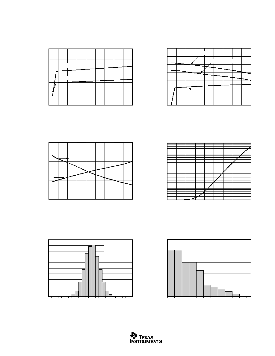
PSRR AND CMRR vs FREQUENCY
10
PSRR, CMRR (dB)
Frequency (Hz)
100
1k
10k
100k
1M
10M
100
80
60
40
20
0
PSRR
CMRR
MAXIMUM OUTPUT VOLTAGE vs FREQUENCY
Output Voltage (Vp-p)
Frequency (Hz)
1k
10k
1M
100k
10M
6
5
4
3
2
1
0
V
S
= 5.5V
V
S
= 5V
V
S
= 2.5V
CHANNEL SEPARATION vs FREQUENCY
10
Channel Separation (dB)
Frequency (Hz)
100
1k
10k
100k
1M
10M
140
120
100
80
60
OUTPUT VOLTAGE SWING vs OUTPUT CURRENT
0
Output Voltage Swing (V)
Output Current (mA)
5
10
≠40
∞
C
≠40
∞
C
+125
∞
C
+125
∞
C
+25
∞
C
V
S
=
±
2.5V
+25
∞
C
15
20
2.5
2
1.5
1
0.5
0
≠0.5
≠1
≠1.5
≠2
≠2.5
Sourcing Current
Sinking Current
OPEN-LOOP GAIN AND PHASE vs FREQUENCY
0.1
Open-Loop Gain (dB)
0
≠45
≠90
≠135
≠180
Phase (
∞
)
Frequency (Hz)
1
100
10
10k
1k
100k
1M
10M
140
120
100
80
60
40
20
0
≠20
Gain
Phase
QUIESCENT AND SHORT-CIRCUIT CURRENT
vs SUPPLY VOLTAGE
2
Quiescent Current (
µ
A)
13
10
7
4
1
Short-Circuit Current (mA)
Supply Voltage (V)
2.5
3
3.5
4
4.5
5
5.5
65
55
45
35
25
I
Q
I
SC
OPA348, 2348, 4348
5
SBOS213C
www.ti.com
TYPICAL CHARACTERISTICS
(Cont.)
At T
A
= +25
∞
C, R
L
= 100k
connected to V
S
/ 2 and V
OUT
= V
S
/ 2, unless otherwise noted.
OPEN-LOOP GAIN AND PSRR vs TEMPERATURE
≠75
Open-Loop Gain and
Power Supply Rejection (dB)
Temperature (
∞
C)
≠50
≠25
0
25
50
75
100
125
150
130
120
110
100
90
80
70
60
A
OL
, R
L
= 100k
A
OL
, R
L
= 5k
PSRR
OFFSET VOLTAGE DRIFT MAGNITUDE
PRODUCTION DISTRIBUTION
Percentage of Amplifiers (%)
Offset Voltage Drift (
µ
V/
∞
C)
1
2
3
4
5
6
7
8
9
10
11
12
25
20
15
10
5
0
Typical production
distribution of
packaged units.
COMMON-MODE REJECTION vs TEMPERATURE
≠75
Common-Mode Rejection (dB)
Temperature (
∞
C)
≠50
≠25
0
25
50
75
100
125
150
100
90
80
70
60
50
V≠ < V
CM
< (V+) ≠ 1.7V
V≠ < V
CM
< V+
QUIESCENT AND SHORT-CIRCUIT CURRENT
vs TEMPERATURE
Quiescent Current (
µ
A)
Temperature (
∞
C)
I
SC
I
Q
75
65
55
45
35
25
15
Short-Circuit Current (mA)
16
14
12
10
8
6
4
≠75
≠50
≠25
0
25
50
75
100
125
150
INPUT BIAS (I
B
) CURRENT vs TEMPERATURE
Input Bias Current (pA)
10k
1k
100
10
1
0.1
≠75
Temperature (
∞
C)
≠50
≠25
0
25
50
75
100
125
150
≠6
≠5
≠4
≠3
≠2
≠1
0
1
2
3
4
5
6
OFFSET VOLTAGE PRODUCTION DISTRIBUTION
Offset Voltage (mV)
20
18
16
14
12
10
8
6
4
2
0
Percent of Amplifiers (%)
Typical production
distribution of
packaged units.
OPA348, 2348, 4348
6
SBOS213C
www.ti.com
TYPICAL CHARACTERISTICS
(Cont.)
At T
A
= +25
∞
C, R
L
= 100k
connected to V
S
/ 2 and V
OUT
= V
S
/ 2, unless otherwise noted.
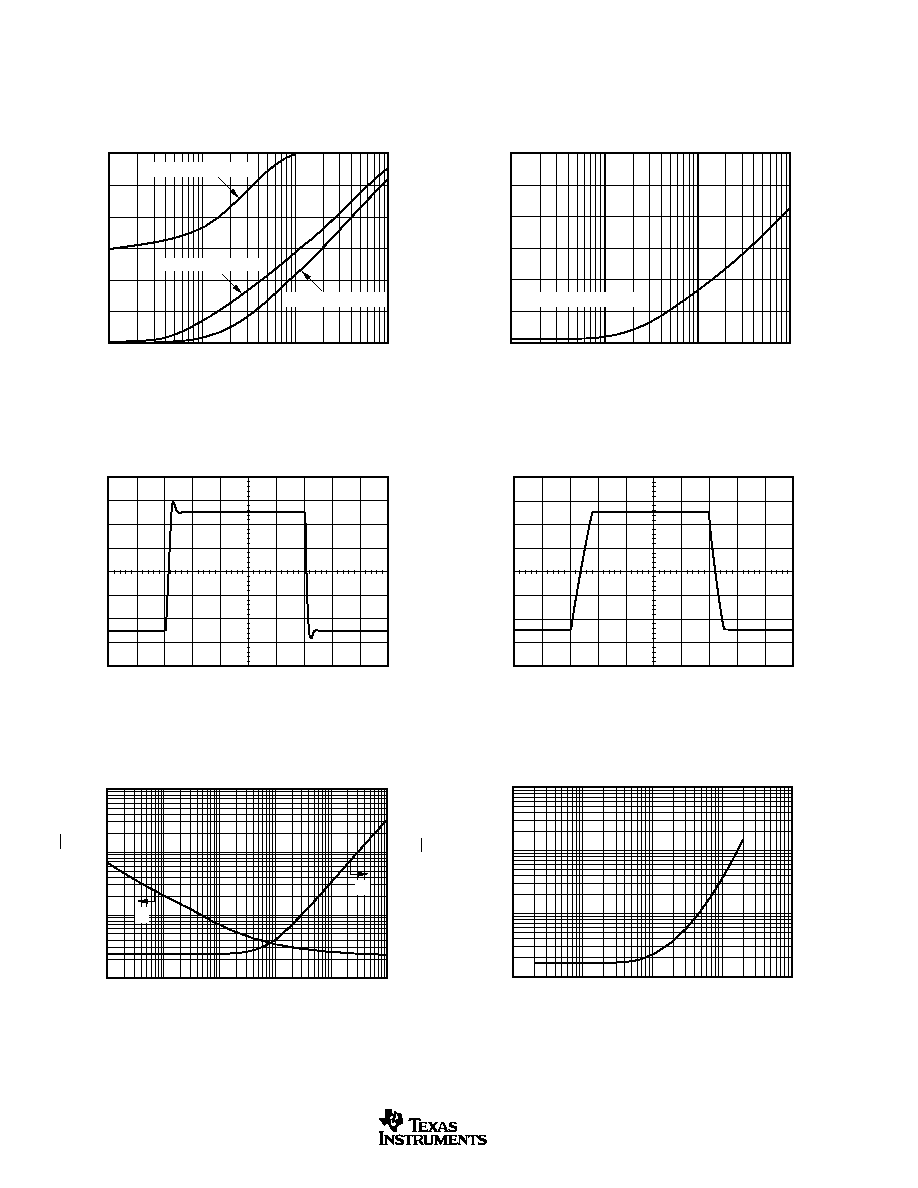
SMALL-SIGNAL OVERSHOOT
vs LOAD CAPACITANCE
10
Small-Signal Overshoot (%)
Load Capacitance (pF)
100
1k
10k
60
50
40
30
20
10
0
G = +1V/V, R
L
= 100k
G = ≠1V/V, R
FB
= 5k
G = ≠1V/V, R
FB
= 100k
PERCENT OVERSHOOT vs LOAD CAPACITANCE
Overshoot (%)
Load Capacitance (pF)
10
100
1k
10k
60
50
40
30
20
10
0
G =
±
5V/V, R
FB
= 100k
SMALL-SIGNAL STEP RESPONSE
G = +1V/V, R
L
= 100k
, C
L
= 100pF
20mV/div
2
µ
s/div
LARGE-SIGNAL STEP RESPONSE
G = +1V/V, R
L
= 100k
, C
L
= 100pF
500mV/div
10
µ
s/div
INPUT CURRENT AND VOLTAGE NOISE
SPECTRAL DENSITY vs FREQUENCY
1
Voltage Noise (nV/
Hz)
Current Noise (fA
Hz)
Frequency (Hz)
10
100
1k
10k
100k
10k
1k
100
10
1k
100
10
1
e
N
i
N
TOTAL HARMONIC DISTORTION + NOISE
vs FREQUENCY
10
Total Harmonic Distortion + Noise (%)
Frequency (Hz)
100
1k
10k
100k
1.000
0.100
0.010
0.001
OPA348, 2348, 4348
7
SBOS213C
www.ti.com
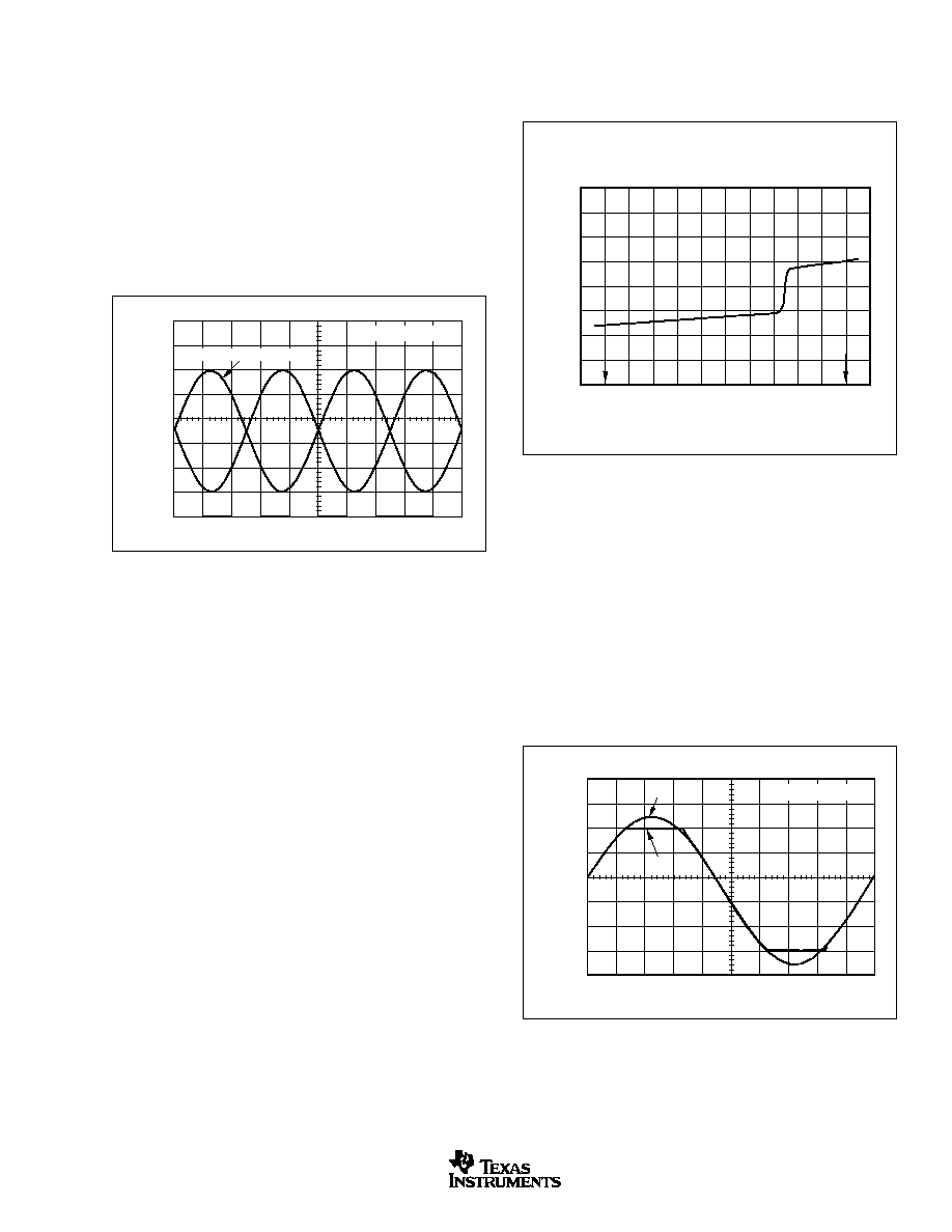
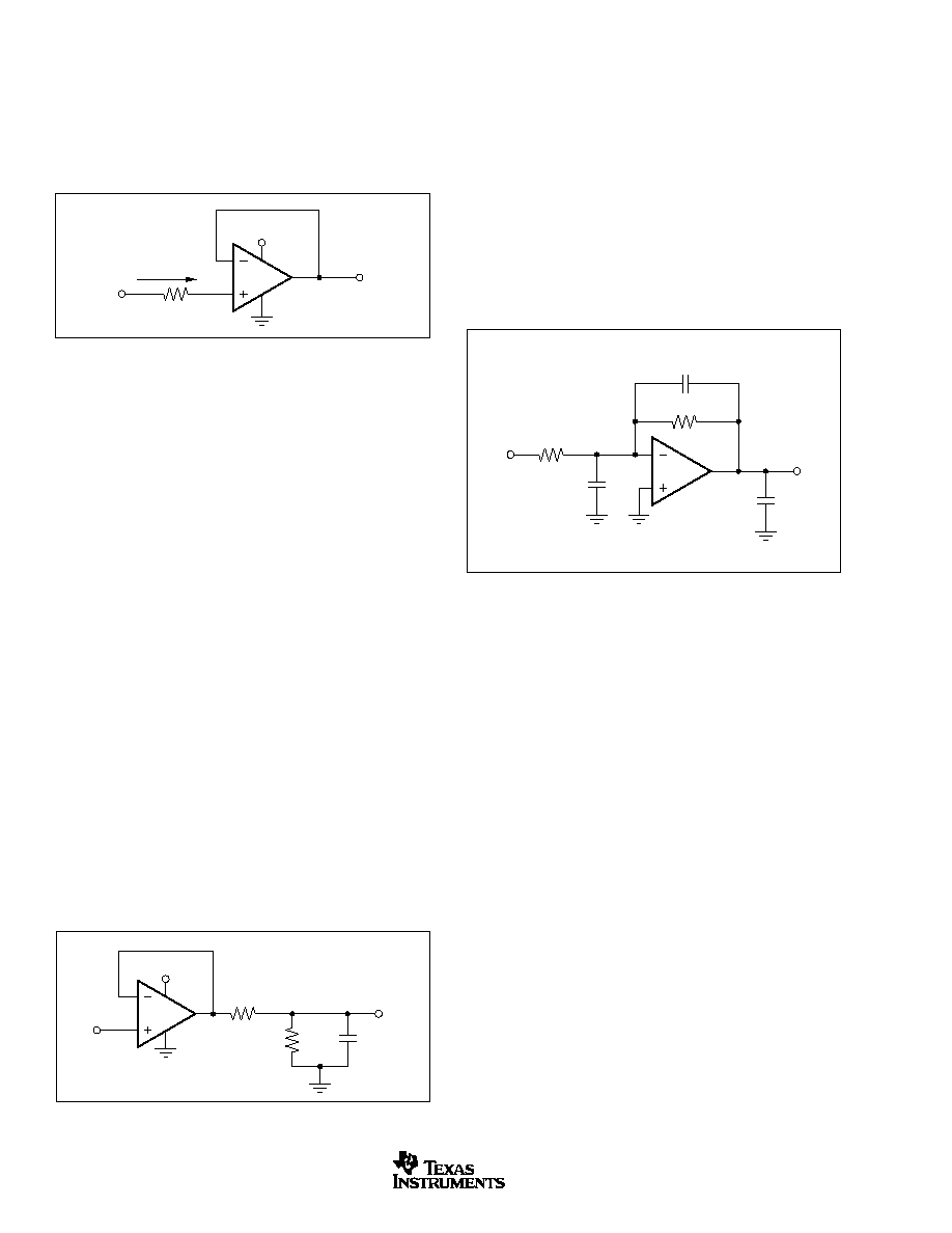
FIGURE 3. OPA348--No Phase Inversion with Inputs Greater
than the Power-Supply Voltage.
APPLICATIONS INFORMATION
OPA348 series op amps are unity-gain stable and suitable
for a wide range of general-purpose applications.
The OPA348 series features wide bandwidth and unity-gain
stability with rail-to-rail input and output for increased dynamic
range. Figure 1 shows the input and output waveforms for the
OPA348 in unity-gain configuration. Operation is from a single
+5V supply with a 100k
load connected to V
S
/2. The input is
a 5Vp-p sinusoid. Output voltage is approximately 4.98Vp-p.
Power-supply pins should be bypassed with 0.01
µ
F ceramic
capacitors.
on the high end. Within the 200mV transition region PSRR,
CMRR, offset voltage, offset drift, and THD may be degraded
compared to operation outside this region.
FIGURE 1. The OPA348 Features Rail-to-Rail Input/Output.
5V
1V/div
0V
G = +1V/V, V
S
= +5V
20
µ
s/div
Output (Inverted on Scope)
OPERATING VOLTAGE
OPA348 series op amps are fully specified and tested from
+2.5V to +5.5V. However, supply voltage may range from
+2.1V to +5.5V. Parameters are tested over the specified
supply range--a unique feature of the OPA348 series. In
addition, all temperature specifications apply from ≠40
∞
C to
+125
∞
C. Most behavior remains virtually unchanged through-
out the full operating voltage range. Parameters that vary
significantly with operating voltages or temperature are shown
in the Typical Characteristics.
COMMON-MODE VOLTAGE RANGE
The input common-mode voltage range of the OPA348 series
extends 200mV beyond the supply rails. This is achieved
with a complementary input stage--an N-channel input differ-
ential pair in parallel with a P-channel differential pair. The
N-channel pair is active for input voltages close to the positive
rail, typically (V+) ≠ 1.2V to 300mV above the positive supply,
while the P-channel pair is on for inputs from 300mV below the
negative supply to approximately (V+) ≠ 1.4V. There is a small
transition region, typically (V+) ≠ 1.4V to (V+) ≠ 1.2V, in which
both pairs are on. This 200mV transition region, shown in
Figure 2, can vary
±
300mV with process variation. Thus, the
transition region (both stages on) can range from (V+) ≠ 1.7V
to (V+) ≠ 1.5V on the low end, up to (V+) ≠ 1.1V to (V+) ≠ 0.9V
RAIL-TO-RAIL INPUT
The input common-mode range extends from (V≠) ≠ 0.2V to
(V+) + 0.2V. For normal operation, inputs should be limited to
this range. The absolute maximum input voltage is 500mV
beyond the supplies. Inputs greater than the input common-
mode range but less than the maximum input voltage, while not
valid, will not cause any damage to the op amp. Unlike some
other op amps, if input current is limited the inputs may go
beyond the power supplies without phase inversion, as shown
in Figure 3.
5V
1V/div
0V
G = +1V/V, V
S
= +5V
10
µ
s/div
V
IN
V
OUT
≠0.5
Offset Voltage (mV)
Common-Mode Voltage (V)
OFFSET VOLTAGE
vs FULL COMMON-MODE VOLTAGE RANGE
0
V≠
0.5
1.5
1
2.5
2
3.5
3
4.5
5
4
5.5
2
1.5
1
0.5
0
≠0.5
≠1
≠1.5
≠2
V+
FIGURE 2. Behavior of Typical Transition Region at Room
Temperature.
OPA348, 2348, 4348
8
SBOS213C
www.ti.com
In unity-gain inverter configuration, phase margin can be
reduced by the reaction between the capacitance at the op
amp input, and the gain setting resistors, thus degrading
capacitive load drive. Best performance is achieved by using
small valued resistors. For example, when driving a 500pF
load, reducing the resistor values from 100k
to 5k
de-
creases overshoot from 55% to 13% (see the typical charac-
teristic "Small-Signal Overshoot vs. Load Capacitance").
However, when large valued resistors cannot be avoided, a
small (4pF to 6pF) capacitor, C
FB
, can be inserted in the
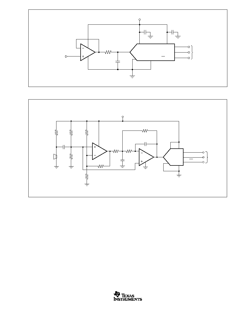
feedback, as shown in Figure 6. This significantly reduces
overshoot by compensating the effect of capacitance, C
IN
,
which includes the amplifier's input capacitance and PC
board parasitic capacitance.
FIGURE 6. Improving Capacitive Load Drive.
Normally, input currents are 0.5pA. However, large inputs
(greater than 500mV beyond the supply rails) can cause
excessive current to flow in or out of the input pins. There-
fore, as well as keeping the input voltage below the maxi-
mum rating, it is also important to limit the input current to
less than 10mA. This is easily accomplished with an input
voltage resistor, as shown in Figure 4.
R
I
OPA348
V
IN
V
OUT
R
F
C
FB
C
IN
C
L
FIGURE 4. Input Current Protection for Voltages Exceeding
the Supply Voltage.
5k
OPA348
10mA max
+5V
V
IN
V
OUT
I
OVERLOAD
RAIL-TO-RAIL OUTPUT
A class AB output stage with common-source transistors is
used to achieve rail-to-rail output. This output stage is ca-
pable of driving 5k
loads connected to any potential be-
tween V+ and ground. For light resistive loads (> 100k
), the
output voltage can typically swing to within 18mV from supply
rail. With moderate resistive loads (10k
to 50k
), the output
voltage can typically swing to within 100mV of the supply
rails while maintaining high open-loop gain (see the typical
characteristic "Output Voltage Swing vs Output Current").
CAPACITIVE LOAD AND STABILITY
The OPA348 in a unity-gain configuration can directly drive
up to 250pF pure capacitive load. Increasing the gain en-
hances the amplifier's ability to drive greater capacitive loads
(see the typical characteristic "Small-Signal Overshoot vs
Capacitive Load"). In unity-gain configurations, capacitive
load drive can be improved by inserting a small (10
to 20
)
resistor, R
S
, in series with the output, as shown in Figure 5.
This significantly reduces ringing while maintaining DC per-
formance for purely capacitive loads. However, if there is a
resistive load in parallel with the capacitive load, a voltage
divider is created, introducing a Direct Current (DC) error at
the output and slightly reducing the output swing. The error
introduced is proportional to the ratio R
S
/ R
L
, and is generally
negligible.
FIGURE 5. Series Resistor in Unity-Gain Buffer Configura-
tion Improves Capacitive Load Drive.
10
to
20
OPA348
V+
V
IN
V
OUT
R
S
R
L
C
L
DRIVING A/D CONVERTERS
The OPA348 series op amps are optimized for driving
medium-speed sampling Analog-to-Digital Converters (ADCs).
The OPA348 op amps buffer the ADCs input capacitance
and resulting charge injection while providing signal gain.
The OPA348 in a basic noninverting configuration driving the
ADS7822, see Figure 7. The ADS7822 is a 12-bit,
microPOWER sampling converter in the MSOP-8 package.
When used with the low-power, miniature packages of the
OPA348, the combination is ideal for space-limited, low-
power applications. In this configuration, an RC network at
the ADC's input can be used to provide for anti-aliasing filter
and charge injection current.
The OPA348 in noninverting configuration driving ADS7822
limited, low-power applications. In this configuration, an RC
network at the ADC's input can be used to provide for anti-
aliasing filter and charge injection current. See Figure 8 for
the OPA2348 driving an ADS7822 in a speech bandpass
filtered data acquisition system. This small, low-cost solution
provides the necessary amplification and signal conditioning
to interface directly with an electret microphone. This circuit
will operate with V
S
= 2.7V to 5V with less than 250
µ
A typical
quiescent current.
OPA348, 2348, 4348
9
SBOS213C
www.ti.com
FIGURE 8. OPA2348 as a Speech Bandpass Filtered Data Acquisition System.
FIGURE 7. OPA348 in Noninverting Configuration Driving ADS7822.
ADS7822
12-Bit A/D
DCLOCK
D
OUT
CS/SHDN
OPA348
+5V
V
IN
V+
2
+In
3
≠In
V
REF
8
4
GND
Serial
Interface
1
0.1
µ
F
0.1
µ
F
7
6
5
NOTE: A/D Input = 0 to V
REF
V
IN
= 0V to 5V for
0V to 5V output.
RC network filters high frequency noise.
500
3300pF
C
3
33pF
V+
GND
3
1
8
4
5
6
7
≠IN
+IN
2
C
2
DCLOCK
Serial
Interface
1000pF
R
1
1.5k
R
4
20k
R
5
20k
R
6
100k
R
8
150k
R
9
510k
R
7
51k
D
OUT
V
REF
V+ = +2.7V to 5V
CS/SHDN
C
1
1000pF
Electret
Microphone
(1)
G = 100
Passband 300Hz to 3kHz
R
3
1M
R
2
1M
NOTE: (1) Electret microphone
powered by R
1
.
ADS7822
12-Bit A/D
1/2
OPA2348
1/2
OPA2348
OPA348, 2348, 4348
10
SBOS213C
www.ti.com
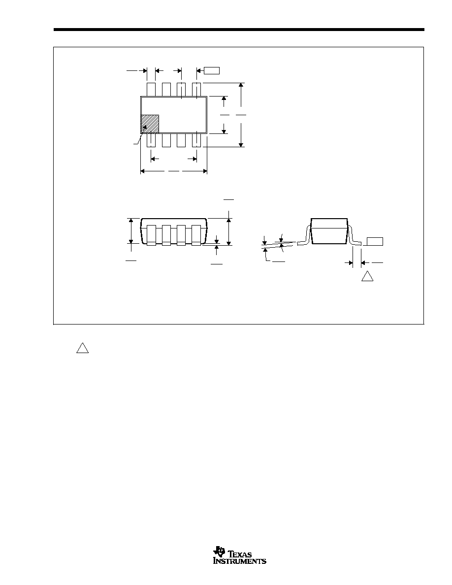
PACKAGE DRAWINGS
MPDS018E ≠ FEBRUARY 1996 ≠ REVISED FEBRUARY 2002
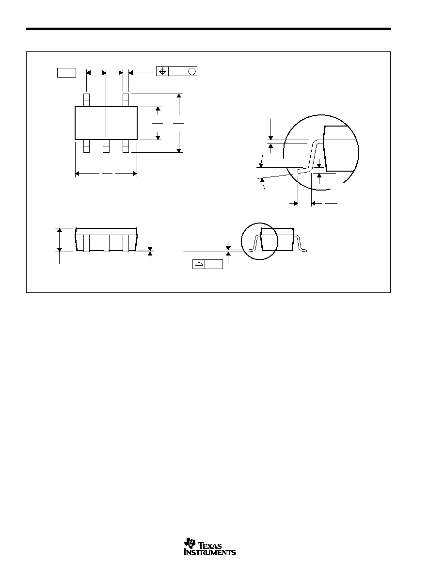
DBV (R-PDSO-G5)
PLASTIC SMALL-OUTLINE
0,10
M
0,20
0,95
0
∞
≠ 8
∞
0,25
0,35
0,55
Gage Plane
0,15 NOM
4073253-4/G 01/02
2,60
3,00
0,50
0,30
1,50
1,70
4
5
3
1
2,80
3,00
0,95
1,45
0,05 MIN
Seating Plane
NOTES: A. All linear dimensions are in millimeters.
B. This drawing is subject to change without notice.
C. Body dimensions do not include mold flash or protrusion.
D. Falls within JEDEC MO-178
OPA348, 2348, 4348
11
SBOS213C
www.ti.com
PACKAGE DRAWINGS (Cont.)
MSOI002B ≠ JANUARY 1995 ≠ REVISED SEPTEMBER 2001
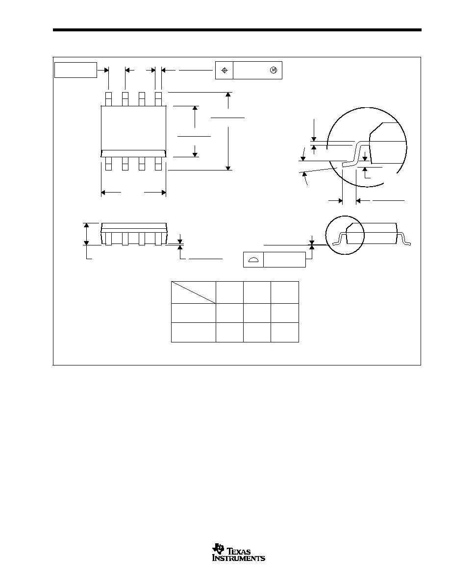
D (R-PDSO-G**)
PLASTIC SMALL-OUTLINE PACKAGE
8 PINS SHOWN
8
0.197
(5,00)
A MAX
A MIN
(4,80)
0.189
0.337
(8,55)
(8,75)
0.344
14
0.386
(9,80)
(10,00)
0.394
16
DIM
PINS **
4040047/E 09/01
0.069 (1,75) MAX
Seating Plane
0.004 (0,10)
0.010 (0,25)
0.010 (0,25)
0.016 (0,40)
0.044 (1,12)
0.244 (6,20)
0.228 (5,80)
0.020 (0,51)
0.014 (0,35)
1
4
8
5
0.150 (3,81)
0.157 (4,00)
0.008 (0,20) NOM
0
∞
≠ 8
∞
Gage Plane
A
0.004 (0,10)
0.010 (0,25)
0.050 (1,27)
NOTES: A. All linear dimensions are in inches (millimeters).
B. This drawing is subject to change without notice.
C. Body dimensions do not include mold flash or protrusion, not to exceed 0.006 (0,15).
D. Falls within JEDEC MS-012

OPA348, 2348, 4348
12
SBOS213C
www.ti.com
MPDS025A ≠ FEBRUARY 1997 ≠ REVISED JUNE 1999
DCK (R-PDSO-G5)
PLASTIC SMALL-OUTLINE
0,10
M
0,10
0,65
0
∞
≠8
∞
0,15
0,46
0,26
Gage Plane
0,13 NOM
4093553/B 06/99
0,15
0,30
1,40
1,10
2,30
1,90
4
5
2,15
1,85
1
3
1,10
0,80
0,10
0,00
Seating Plane
NOTES: A. All linear dimensions are in millimeters.
B. This drawing is subject to change without notice.
C. Body dimensions do not include mold flash or protrusion.
D. Falls within JEDEC MO-203
PACKAGE DRAWINGS (Cont.)
OPA348, 2348, 4348
13
SBOS213C
www.ti.com
PACKAGE DRAWINGS (Cont.)
MPDS099 ≠ MARCH 2001
DCN (R-PDSO-G8)
PLASTIC SMALL-OUTLINE
C
4202106/A 03/01
3,00
2,80
3,00
2,60
1,50
1,75
Area
0,28
0,45
0
∞
≠10
∞
0,09
0,20
1,30
0,90
0,10
0,60
Index
0,00
0,15
≠A≠
0,65
0,90
1,45
1,95 REF
NOTES: A. All linear dimensions are in millimeters.
B. This drawing is subject to change without notice.
C. Foot length measured reference to flat foot surface
parallel to Datum A.
D. Package outline exclusive of mold flash, metal burr and
dambar protrusion/intrusion.
E. Package outline inclusive of solder plating.
F. A visual index feature must be located within the
cross-hatched area.
OPA348, 2348, 4348
14
SBOS213C
www.ti.com
PACKAGE DRAWINGS (Cont.)
MTSS001C ≠ JANUARY 1995 ≠ REVISED FEBRUARY 1999
PW (R-PDSO-G**)
PLASTIC SMALL-OUTLINE PACKAGE
14 PINS SHOWN
0,65
M
0,10
0,10
0,25
0,50
0,75
0,15 NOM
Gage Plane
28
9,80
9,60
24
7,90
7,70
20
16
6,60
6,40
4040064/F 01/97
0,30
6,60
6,20
8
0,19
4,30
4,50
7
0,15
14
A
1
1,20 MAX
14
5,10
4,90
8
3,10
2,90
A MAX
A MIN
DIM
PINS **
0,05
4,90
5,10
Seating Plane
0
∞
≠ 8
∞
NOTES: A. All linear dimensions are in millimeters.
B. This drawing is subject to change without notice.
C. Body dimensions do not include mold flash or protrusion not to exceed 0,15.
D. Falls within JEDEC MO-153

PACKAGING INFORMATION
ORDERABLE DEVICE
STATUS(1)
PACKAGE TYPE
PACKAGE DRAWING
PINS
PACKAGE QTY
OPA2348AID
ACTIVE
SOIC
D
8
100
OPA2348AIDCNR
ACTIVE
SSOP
DCN
8
3000
OPA2348AIDCNT
ACTIVE
SSOP
DCN
8
250
OPA2348AIDR
ACTIVE
SOIC
D
8
2500
OPA348AID
ACTIVE
SOIC
D
8
100
OPA348AIDBVR
ACTIVE
SOP
DBV
5
3000
OPA348AIDBVT
ACTIVE
SOP
DBV
5
250
OPA348AIDCKR
ACTIVE
SOP
DCK
5
3000
OPA348AIDCKT
ACTIVE
SOP
DCK
5
250
OPA348AIDR
ACTIVE
SOIC
D
8
2500
OPA4348AID
ACTIVE
SOIC
D
14
58
OPA4348AIDR
ACTIVE
SOIC
D
14
2500
OPA4348AIPWR
ACTIVE
TSSOP
PW
14
2500
OPA4348AIPWT
ACTIVE
TSSOP
PW
14
250
(1) The marketing status values are defined as follows:
ACTIVE: Product device recommended for new designs.
LIFEBUY: TI has announced that the device will be discontinued, and a lifetime-buy period is in effect.
NRND: Not recommended for new designs. Device is in production to support existing customers, but TI does not recommend using this part in
a new design.
PREVIEW: Device has been announced but is not in production. Samples may or may not be available.
OBSOLETE: TI has discontinued the production of the device.
PACKAGE OPTION ADDENDUM
www.ti.com
3-Oct-2003

IMPORTANT NOTICE
Texas Instruments Incorporated and its subsidiaries (TI) reserve the right to make corrections, modifications,
enhancements, improvements, and other changes to its products and services at any time and to discontinue
any product or service without notice. Customers should obtain the latest relevant information before placing
orders and should verify that such information is current and complete. All products are sold subject to TI's terms
and conditions of sale supplied at the time of order acknowledgment.
TI warrants performance of its hardware products to the specifications applicable at the time of sale in
accordance with TI's standard warranty. Testing and other quality control techniques are used to the extent TI
deems necessary to support this warranty. Except where mandated by government requirements, testing of all
parameters of each product is not necessarily performed.
TI assumes no liability for applications assistance or customer product design. Customers are responsible for
their products and applications using TI components. To minimize the risks associated with customer products
and applications, customers should provide adequate design and operating safeguards.
TI does not warrant or represent that any license, either express or implied, is granted under any TI patent right,
copyright, mask work right, or other TI intellectual property right relating to any combination, machine, or process
in which TI products or services are used. Information published by TI regarding third-party products or services
does not constitute a license from TI to use such products or services or a warranty or endorsement thereof.
Use of such information may require a license from a third party under the patents or other intellectual property
of the third party, or a license from TI under the patents or other intellectual property of TI.
Reproduction of information in TI data books or data sheets is permissible only if reproduction is without
alteration and is accompanied by all associated warranties, conditions, limitations, and notices. Reproduction
of this information with alteration is an unfair and deceptive business practice. TI is not responsible or liable for
such altered documentation.
Resale of TI products or services with statements different from or beyond the parameters stated by TI for that
product or service voids all express and any implied warranties for the associated TI product or service and
is an unfair and deceptive business practice. TI is not responsible or liable for any such statements.
Following are URLs where you can obtain information on other Texas Instruments products and application
solutions:
Products
Applications
Amplifiers
amplifier.ti.com
Audio
www.ti.com/audio
Data Converters
dataconverter.ti.com
Automotive
www.ti.com/automotive
DSP
dsp.ti.com
Broadband
www.ti.com/broadband
Interface
interface.ti.com
Digital Control
www.ti.com/digitalcontrol
Logic
logic.ti.com
Military
www.ti.com/military
Power Mgmt
power.ti.com
Optical Networking
www.ti.com/opticalnetwork
Microcontrollers
microcontroller.ti.com
Security
www.ti.com/security
Telephony
www.ti.com/telephony
Video & Imaging
www.ti.com/video
Wireless
www.ti.com/wireless
Mailing Address:
Texas Instruments
Post Office Box 655303 Dallas, Texas 75265
Copyright
2003, Texas Instruments Incorporated