1
µ
A, Rail-to-Rail I/O CMOS
OPERATIONAL AMPLIFIERS
FEATURES
q
LOW SUPPLY CURRENT: 1
µ
A
q
GAIN-BANDWIDTH: 70kHz
q
UNITY GAIN STABLE
q
LOW INPUT BIAS CURRENT: 10pA (max)
q
WIDE SUPPLY RANGE: 1.8V to 5.5V
q
INPUT RANGE 200mV BEYOND RAILS
q
OUTPUT SWINGS TO 150mV OF RAILS
q
OUTPUT DRIVE CURRENT: 8mA
q
OPEN-LOOP GAIN: 90dB
q
Micro
PACKAGES: SC70, SOT23-5, SOT23-8
APPLICATIONS
q
BATTERY PACKS AND POWER SUPPLIES
q
PORTABLE PHONES, PAGERS, AND CAMERAS
q
SOLAR-POWERED SYSTEMS
q
SMOKE, GAS, AND FIRE DETECTION SYSTEMS
q
REMOTE SENSORS
q
PCMCIA CARDS
q
DRIVING A/D CONVERTERS
q
Micro
POWER FILTERS
DESCRIPTION
The OPA349 and the OPA2349 are ultra-low power opera-
tional amplifiers that provide 70kHz bandwidth with only 1
µ
A
quiescent current. These rail-to-rail input and output amplifi-
ers are specifically designed for battery-powered applica-
tions. The input common-mode voltage range extends 200mV
beyond the power supply rails and the output swings to within
150mV of the rails, maintaining wide dynamic range. Unlike
some micropower op amps, these parts are unity-gain stable
and require no external compensation to achieve wide band-
width. The OPA349 features a low input bias current that
allows the use of large source and feedback resistors.
OPA349 can be operated with power supplies from 1.8V to
5.5V with little change in performance, ensuring continuing
superior performance even in low battery situations.
OPA349 comes in the miniature SOT23-5, SC70, and SO-8
surface mount packages. OPA2349 dual is available in the
SOT23-8, and SO-8 surface-mount packages. These tiny
packages are ideal for use in high-density applications, such
as PCMCIA cards, battery packs, and portable instruments.
The OPA349 is specified for ≠40
∞
C to +125
∞
C. The OPA2349
is specified for ≠40
∞
C to +70
∞
C.
OPA349
OPA2349
SBOS121A ≠ APRIL 2002
PRODUCTION DATA information is current as of publication date.
Products conform to specifications per the terms of Texas Instruments
standard warranty. Production processing does not necessarily include
testing of all parameters.
Copyright © 2000, Texas Instruments Incorporated
Please be aware that an important notice concerning availability, standard warranty, and use in critical applications of
Texas Instruments semiconductor products and disclaimers thereto appears at the end of this data sheet.
FEATURES
PRODUCT
1
µ
A, 5.5kHz, Rail-To-Rail
TLV240x
1
µ
A, 5.5kHz, Rail-To-Rail
TLV224x
7
µ
A, 160kHz, Rail-To-Rail, 2.7V to 16V Supply
TLV238x
7
µ
A, 160kHz, Rail-To-Rail, Micro Power
TLV27Lx
20
µ
A, 500kHz, Rail-To-Rail, 1.8V Micro Power
TLV276x
20
µ
A, 350kHz, Rail-To-Rail, Micro Power
OPAx347
45
µ
A, 1MHz, Rail-To-Rail, 2.1V to 5.5V Supply
OPAx348
OPAX349 RELATED PRODUCTS
OPA3
49
OPA2349
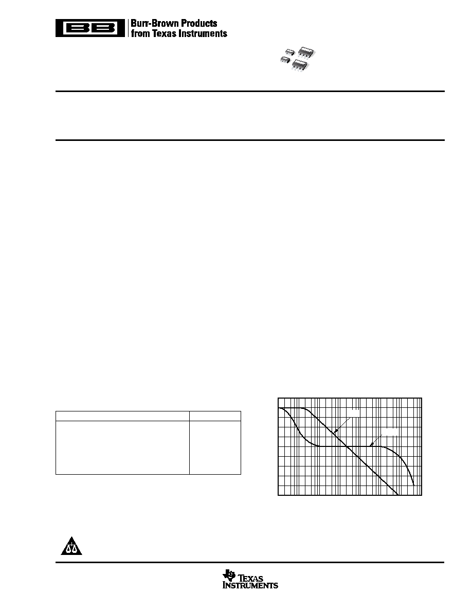
OPEN-LOOP GAIN AND PHASE vs FREQUENCY
Frequency (Hz)
Gain (dB)
Phase (
∞
)
100
90
80
70
60
50
40
30
20
10
0
0
45
90
135
180
1
10
100
1k
10k
100k
1M
0.1
Gain
Phase
www.ti.com
OPA349, 2349
2
SBOS121A
www.ti.com
Supply Voltage, V+ to V≠ ................................................................... 5.5V
Signal Input Terminals, Voltage
(2)
.................. (V≠) ≠ 0.5V to (V+) + 0.5V
Current
(2)
.................................................... 10mA
Output Short Circuit
(3)
.............................................................. Continuous
Operating Temperature .................................................. ≠55
∞
C to +125
∞
C
Storage Temperature ..................................................... ≠65
∞
C to +150
∞
C
Junction Temperature ...................................................................... 150
∞
C
Lead Temperature (soldering, 3s) ................................................... 300
∞
C
NOTES: (1) Stresses above these ratings may cause permanent damage.
Exposure to absolute maximum conditions for extended periods may de-
grade device reliability. These are stress ratings only, and functional opera-
tion of the device at these, or any other conditions beyond those specified,
is not implied. (2) Input terminals are diode-clamped to the power supply
rails. Input signals that can swing more than 0.5V beyond the supply rails
should be current-limited to 10mA or less. (3) Short circuit to ground, one
amplifier per package.
ABSOLUTE MAXIMUM RATINGS
(1)
PACKAGE/ORDERING INFORMATION
SPECIFIED
PACKAGE
TEMPERATURE
PACKAGE
ORDERING
TRANSPORT
PRODUCT
PACKAGE
DESIGNATOR
(1)
RANGE
MARKING
NUMBER
(2)
MEDIA, QUANTITY
Single
OPA349NA
SOT23-5
DBV
≠40
∞
C to +125
∞
C
A49
OPA349NA /250
Tape and Reel, 250
"
"
"
"
"
OPA349NA/3K
Tape and Reel, 3000
OPA349UA
SO-8
D
≠40
∞
C to +125
∞
C
OPA349UA
OPA349UA
Rails, 100
"
"
"
"
"
OPA349UA/2K5
Tape and Reel, 2500
OPA349SA
SC70-5
DCK
≠40
∞
C to +125
∞
C
S49
OPA349SA/250
Tape and Reel, 250
"
"
"
"
"
OPA349SA/3K
Tape and Reel, 3000
Dual
OPA2349EA
SOT23-8
DCN
≠40
∞
C to +70
∞
C
C49
OPA2349EA/250
Tape and Reel, 250
"
"
"
"
"
OPA2349EA/3K
Tape and Reel, 3000
OPA2349UA
SO-8
D
≠40
∞
C to +70
∞
C
OPA2349UA
OPA2349UA
Rails, 100
"
"
"
"
"
OPA2349UA/2K5
Tape and Reel, 2500
NOTE: (1) For the most current specifications and package information, refer to our web site at www.ti.com. (2) Models with a (/) are available only in Tape and
Reel in the quantities indicated (e.g., /3K indicates 3000 devices per reel). Ordering 3000 pieces of "OPA2349EA/3K" will get a single 3000-piece Tape and Reel.
1
2
3
5
4
V+
≠In
Out
V≠
+In
OPA349
SOT23-5
1
2
3
4
8
7
6
5
NC
(1)
V+
Out
NC
(1)
NC
(1)
≠In
+In
V≠
OPA349
SO-8
1
2
3
4
8
7
6
5
V+
Out B
≠In B
+In B
Out A
≠In A
+In A
V≠
OPA2349
SOT23-8, SO-8
ELECTROSTATIC
DISCHARGE SENSITIVITY
This integrated circuit can be damaged by ESD. Texas Instru-
ments recommends that all integrated circuits be handled with
appropriate precautions. Failure to observe proper handling
and installation procedures can cause damage.
ESD damage can range from subtle performance degrada-
tion to complete device failure. Precision integrated circuits
may be more susceptible to damage because very small
parametric changes could cause the device not to meet its
published specifications.
PIN CONFIGURATIONS
NOTE: (1) NC indicates no internal connection.
1
2
3
5
4
V+
Out
+In
V≠
≠In
OPA349
SC70-5

OPA349, 2349
3
SBOS121A
www.ti.com
ELECTRICAL CHARACTERISTICS
(Single)
: V
S
= +1.8V to +5.5V
Boldface limits apply over the specified temperature range, T
A
= ≠40
∞
C to +125
∞
C
At T
A
= +25
∞
C, R
L
= 1M
connected to V
S
/2, unless otherwise noted.
PARAMETER
CONDITION
MIN
TYP
MAX
UNITS
OFFSET VOLTAGE
Input Offset Voltage
V
OS
V
S
= 5V, V
CM
= 2.5V
±
2
±
10
mV
Over Temperature
±
2
±
13
mV
Drift
dV
OS
/dT
±
15
µ
V/
∞
C
vs Power Supply
PSRR
V
S
= 1.8V to 5.5V, V
CM
= (V≠) + 0.3V
350
1000
µ
V/V
Over Temperature
3000
µ
V/V
INPUT VOLTAGE RANGE
Common-Mode Voltage Range
V
CM
(V≠) ≠ 0.2
(V+) + 0.2
V
Common-Mode Rejection Ratio
CMRR
V
S
= +5V, ≠0.2V < V
CM
< 3.5V
52
72
dB
Over Temperature
50
dB
V
S
= +5V, ≠0.2V < V
CM
< 5.2V
48
60
dB
Over Temperature
46
dB
INPUT BIAS CURRENT
Input Bias Current
I
B
±
0.5
±
10
pA
Input Offset Current
I
OS
±
1
±
10
pA
INPUT IMPEDANCE
Differential
10
13
|| 2
|| pF
Common-Mode
10
13
|| 4
|| pF
NOISE
Input Voltage Noise, f = 0.1Hz to 10Hz
8
µ
Vp-p
Input Voltage Noise Density, f = 1kHz
e
n
300
nV/
Hz
Current Noise Density, f = 1kHz
i
n
4
fA/
Hz
OPEN-LOOP GAIN
Open-Loop Voltage Gain
A
OL
R
L
= 1M
, V
S
= +5.5V, +0.05V < V
O
< +5.45V
74
90
dB
Over Temperature
72
dB
Open-Loop Voltage Gain
A
OL
R
L
= 10k
, V
S
= +5.5V, +0.15V < V
O
< +5.35V
74
90
dB
Over Temperature
60
dB
OUTPUT
Voltage Output Swing from Rail
R
L
= 1M
, V
S
= +5.5V, A
OL
> 74dB
50
mV
Over Temperature
50
mV
R
L
= 10k
, V
S
= +5.5V, A
OL
> 74dB
150
mV
Over Temperature
150
mV
Output Current
±
8
mA
Short-Circuit Current
I
SC
±
10
mA
Capacitive Load Drive
C
LOAD
See Typical Characteristics
FREQUENCY RESPONSE
C
L
= 10pF
Gain-Bandwidth Product
GBW
G = +1
70
kHz
Slew Rate
SR
V
S
= +5V, G = +1
0.02
V/
µ
s
Settling Time, 0.1%
t
S
V
S
= 5V, 1V Step
65
µ
s
0.01%
V
S
= 5V, 1V Step
80
µ
s
Overload Recovery Time
V
IN
∑ Gain = V
S
5
µ
s
POWER SUPPLY
Specified Voltage Range
1.8
5.5
V
Quiescent Current (per amplifier)
I
Q
I
O
= 0
1
2
µ
A
Over Temperature
2.5
µ
A
TEMPERATURE RANGE
Specified Range
≠40
+125
∞
C
Storage Range
≠65
+150
∞
C
Thermal Resistance
JA
∞
C/W
SOT23-5 Surface Mount
200
∞
C/W
SO-8 Surface Mount
150
∞
C/W
SC70-5 Surface Mount
250
∞
C/W
OPA349NA, UA, SA

OPA349, 2349
4
SBOS121A
www.ti.com
PARAMETER
CONDITION
MIN
TYP
MAX
UNITS
OFFSET VOLTAGE
Input Offset Voltage
V
OS
V
S
= 5V, V
CM
= 2.5V
±
2
±
10
mV
Over Temperature
±
2
±
13
mV
Drift
dV
OS
/dT
±
15
µ
V/
∞
C
vs Power Supply
PSRR
V
S
= 1.8V to 5.5V, V
CM
= (V≠) + 0.3V
350
1000
µ
V/V
Over Temperature
3000
µ
V/V
Channel Separation, dc
R
L
= 100k
10
µ
V/V
f = 1kHz
66
(1)
dB
INPUT VOLTAGE RANGE
Common-Mode Voltage Range
V
CM
(V≠) ≠ 0.2
(V+) + 0.2
V
Common-Mode Rejection Ratio
CMRR
V
S
= +5V, ≠0.2V < V
CM
< 3.5V
52
72
dB
Over Temperature
50
dB
V
S
= +5V, ≠0.2V < V
CM
< 5.2V
48
60
dB
Over Temperature
46
dB
INPUT BIAS CURRENT
Input Bias Current
I
B
±
0.5
±
10
pA
Input Offset Current
I
OS
±
1
±
10
pA
INPUT IMPEDANCE
Differential
10
13
|| 2
|| pF
Common-Mode
10
13
|| 4
|| pF
NOISE
Input Voltage Noise, f = 0.1Hz to 10Hz
8
µ
Vp-p
Input Voltage Noise Density, f = 1kHz
e
n
300
nV/
Hz
Current Noise Density, f = 1kHz
i
n
4
fA/
Hz
OPEN-LOOP GAIN
Open-Loop Voltage Gain
A
OL
R
L
= 1M
, V
S
= +5.5V, +0.3V < V
O
< +5.2V
74
90
dB
Over Temperature
72
dB
Open-Loop Voltage Gain
A
OL
R
L
= 10k
, V
S
= +5.5V, +0.35V < V
O
< +5.15V
74
90
dB
Over Temperature
60
dB
OUTPUT
Voltage Output Swing from Rail
R
L
= 1M
, V
S
= +5.5V, A
OL
> 74dB
150
300
mV
Over Temperature
300
mV
R
L
= 10k
, V
S
= +5.5V, A
OL
> 74dB
200
350
mV
Over Temperature
350
mV
Output Current
±
8
mA
Short-Circuit Current
I
SC
±
10
mA
FREQUENCY RESPONSE
C
L
= 10pF
Gain-Bandwidth Product
GBW
G = +1
70
kHz
Slew Rate
SR
V
S
= +5V, G = +1
0.02
V/
µ
s
Settling Time, 0.1%
t
S
V
S
= 5V, 1V Step
65
µ
s
0.01%
V
S
= 5V, 1V Step
80
µ
s
Overload Recovery Time
V
IN
∑ Gain = V
S
5
µ
s
POWER SUPPLY
Specified Voltage Range
V
S
1.8
5.5
V
Quiescent Current (per amplifier)
I
Q
I
O
= 0
1
2
µ
A
Over Temperature
10
µ
A
TEMPERATURE RANGE
Specified Range
≠40
+70
∞
C
Operating Range
≠40
+85
∞
C
Storage Range
≠65
+150
∞
C
Thermal Resistance
JA
∞
C/W
SOT23-8 Surface Mount
200
∞
C/W
SO-8 Surface Mount
150
∞
C/W
NOTE: (1) Refer to "Typical Characteristics" Curves.
OPA2349EA, UA
ELECTRICAL CHARACTERISTICS
(Dual)
: V
S
= +1.8V to +5.5V
Boldface limits apply over the specified temperature range, T
A
= ≠40
∞
C to +70
∞
C
At T
A
= +25
∞
C, R
L
= 1M
connected to V
S
/2, unless otherwise noted.
OPA349, 2349
5
SBOS121A
www.ti.com
TYPICAL CHARACTERISTICS
At T
A
= +25
∞
C, V
S
= +5V, R
L
= 1M
connected to V
S
/2, unless otherwise noted.
R
L
= 10k
R
L
= 1M
≠75
≠50
≠25
0
25
50
75
100
125
Temperature (
∞
C)
OPEN-LOOP GAIN vs TEMPERATURE
100
95
90
85
80
75
70
65
60
Gain (dB)
Dual Version Operation
above 85
∞
C is not
recommended
≠75
≠50
≠25
0
25
50
75
100
125
Temperature (
∞
C)
COMMON-MODE REJECTION RATIO
vs TEMPERATURE
80
75
70
65
60
55
50
CMRR (dB)
≠0.2V < V
CM
< 3.5V
≠0.2V < V
CM
< 5.2V
Dual Version Operation
above 85
∞
C is not
recommended
POWER-SUPPLY REJECTION RATIO vs FREQUENCY
Frequency (Hz)
PSRR (dB)
100
90
80
70
60
50
40
30
20
10
0
10
100
1k
10k
100k
+PSRR
≠PSRR
80
70
60
50
40
PSRR (dB)
≠75
≠50
≠25
0
25
50
75
100
125
Temperature (
∞
C)
POWER-SUPPLY REJECTION RATIO
vs TEMPERATURE
Dual version
operation above 85
∞
C
is not recommended.
COMMON-MODE REJECTION RATIO vs FREQUENCY
Frequency (Hz)
CMRR (dB)
80
70
60
50
40
30
20
10
0
10
100
1k
10k
100k
OPEN-LOOP GAIN AND PHASE vs FREQUENCY
Frequency (Hz)
Gain (dB)
Phase (
∞
)
100
90
80
70
60
50
40
30
20
10
0
0
45
90
135
180
1
10
100
1k
10k
100k
1M
0.1
Gain
Phase
OPA349, 2349
6
SBOS121A
www.ti.com
TYPICAL CHARACTERISTICS
(Cont.)
At T
A
= +25
∞
C, V
S
= +5V, R
L
= 1M
connected to V
S
/2, unless otherwise noted.
≠75
≠50
≠25
0
25
50
75
100
125
Temperature (
∞
C)
SHORT-CIRCUIT CURRENT vs TEMPERATURE
15
10
5
0
≠5
≠10
≠15
Short-Circuit Current (mA)
V
S
= 5.5V
V
S
= 5V
V
S
= 5V
V
S
= 5.5V
V
S
= 2.5V
V
S
= 2.5V
V
S
= 1.8V
Dual Version Operation above 85
∞
C
is not recommended
OPA2349
OPA349
≠75
≠50
≠25
0
25
50
75
100
125
Temperature (
∞
C)
QUIESCENT CURRENT vs TEMPERATURE
3.0
2.5
2.0
1.5
1.0
0.5
0.0
Quiescent Current (
µ
A)
Dual Version Operation
above 85
∞
C is not
recommended
INPUT BIAS CURRENT vs TEMPERATURE
≠75
Input Bias Current (pA)
Temperature (
∞
C)
≠50
≠25
0
25
50
75
100
125
150
10k
1k
100
10
1
0.1
Dual Version Operation
above 85
∞
C is not
recommended
INPUT VOLTAGE NOISE DENSITY
Frequency (Hz)
Voltage Noise (nV/
Hz)
1000
400
100
10
100
1k
10k
CHANNEL SEPARATION vs FREQUENCY
Frequency (Hz)
Channel Separation (dB)
100
90
80
70
60
50
40
30
20
10
0
10
100
1k
10k
100k
≠40
∞
C
25
∞
C
125
∞
C
12
10
8
6
4
2
1.4
1.2
1
0.8
0.6
0.4
1.5
2.0
2.5
3.0
3.5
4.0
4.5
5.0
5.5
QUIESCENT AND SHORT-CIRCUIT
vs SUPPLY VOLTAGE
Short-Circuit Current (mA)
Quiescent Current (
µ
A)
Quiescent Current
Short-Circuit Current
Supply Voltage (V)
OPA349, 2349
7
SBOS121A
www.ti.com
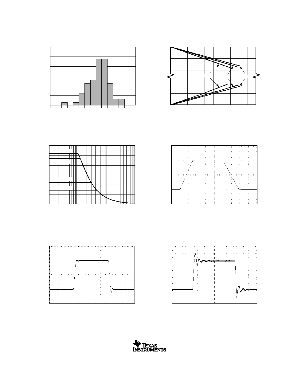
100
µ
s/div
LARGE-SIGNAL STEP RESPONSE
G = 1, R
L
= 1M
1V/div
40
µ
s/div
SMALL-SIGNAL STEP RESPONSE
G = 1, R
L
= 1M
, C
L
= 20pF
50mV/div
100
µ
s/div
SMALL-SIGNAL STEP RESPONSE
G = 1, R
L
= 1M
, C
L
= 500pF
50mV/div
OFFSET VOLTAGE DRIFT
PRODUCTION DISTRIBUTION
Population
Offset Voltage Drift (
µ
V/
∞
C)
≠30 ≠25 ≠20 ≠15 ≠10 ≠5
0
5
10 15 20 25 30
35 40
25
∞
C
125
∞
C
≠55
∞
C
(V+)
(V+) ≠1
(V+) ≠2
(V≠) +2
(V≠) +1
(V≠)
Output V
oltage (V)
0
1
2
3
4
5
6
7
8
10
9
Output Current (mA)
OUTPUT VOLTAGE vs OUTPUT CURRENT
MAXIMUM OUTPUT VOLTAGE vs FREQUENCY
Frequency (Hz)
Output Voltage (Vp-p)
6
5
4
3
2
1
0
100
1k
10k
100k
V
S
= +5.5V
V
S
= +5V
V
S
= +2.5V
V
S
= +1.8V
TYPICAL CHARACTERISTICS
(Cont.)
At T
A
= +25
∞
C, V
S
= +5V, R
L
= 1M
connected to V
S
/2, unless otherwise noted.

OPA349, 2349
8
SBOS121A
www.ti.com
TYPICAL CHARACTERISTICS
(Cont.)
At T
A
= +25
∞
C, V
S
= +5V, R
L
= 1M
connected to V
S
/2, unless otherwise noted.
G = ≠1V/V, R
L
= 1M
G = +1V/V, R
L
= 1M
120
100
80
60
40
20
0
Small-Signal Ov
ershoot (%)
10
100
1K
Load Capacitance (pF)
SMALL-SIGNAL OVERSHOOT vs LOAD CAPACITANCE
OPA349, 2349
9
SBOS121A
www.ti.com
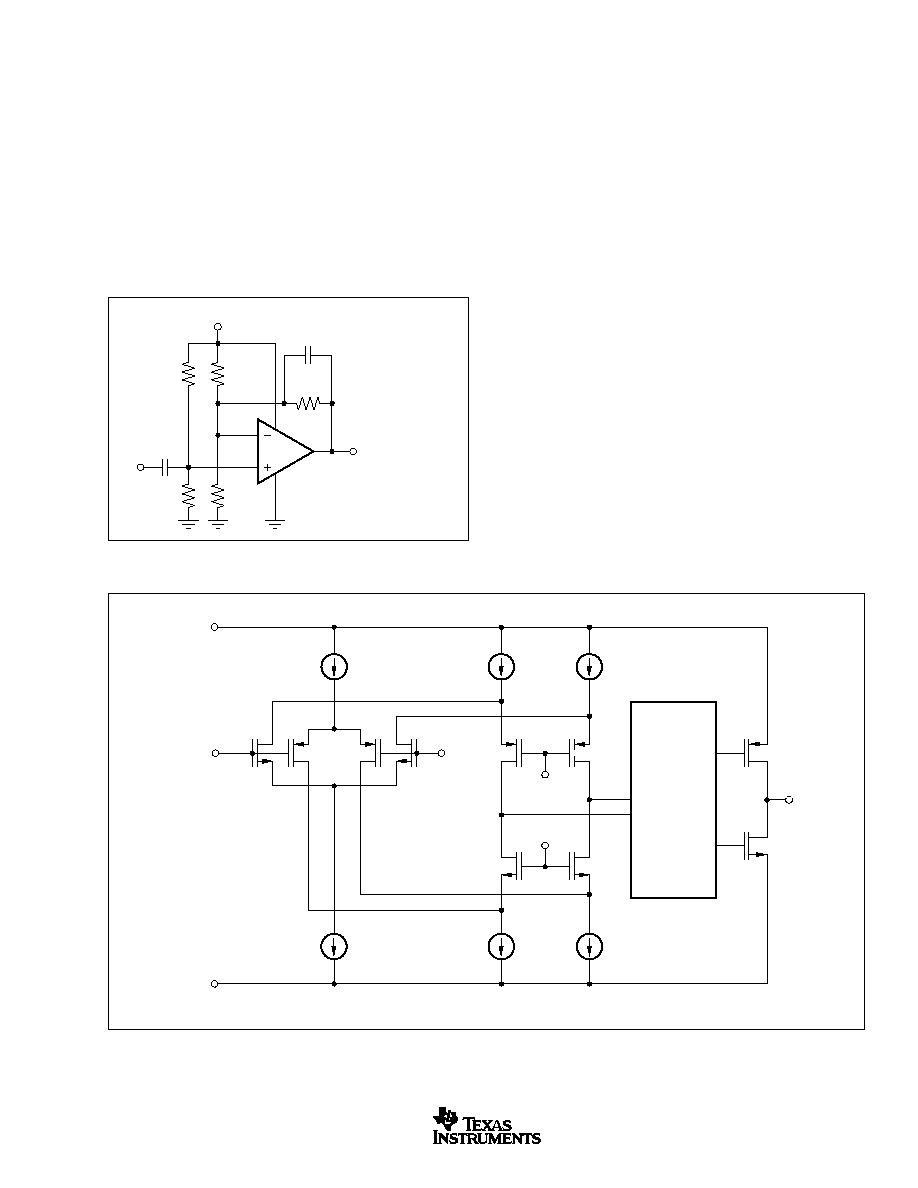
FIGURE 2. Simplified Schematic.
FIGURE 1. AC-Coupled Amplifier.
V
BIAS1
V
BIAS2
V
IN
+
V
IN
≠
Class AB
Control
Circuitry
V
O
V≠
(Ground)
V+
Reference
Current
APPLICATIONS INFORMATION
OPA349 series op amps are unity gain stable and can operate
on a single supply, making them highly versatile and easy to
use. Power supply pins should be bypassed with 0.01
µ
F
ceramic capacitors.
OPA349 series op amps are fully specified and tested from
+1.8V to +5.5V. Parameters that vary significantly with operat-
ing voltages or temperature are shown in the Typical Charac-
teristics Curves.
The ultra low quiescent current of the OPA349 requires
careful applications circuit techniques to achieve low overall
current consumption. Figure 1 shows an ac-coupled amplifier
biased with a voltage divider. Resistor values must be very
large to minimize current. The large feedback resistor value
reacts with input capacitance and stray capacitance to pro-
duce a pole in the feedback network. A feedback capacitor
may be required to assure stability and limit overshoot or
gain peaking. Check circuit performance carefully to assure
that biasing and feedback techniques meet your signal and
quiescent current requirements.
RAIL-TO-RAIL INPUT
The input common-mode voltage range of the OPA349 series
extends 200mV beyond the supply rails. This is achieved with
a complementary input stage--an N-channel input differential
pair in parallel with a P-channel differential pair (as shown in
Figure 2). The N-channel pair is active for input voltages close
to the positive rail, typically (V+) ≠ 1.3V to 200mV above the
positive supply, while the P-channel pair is on for inputs from
200mV below the negative supply to approximately (V+) ≠
1.3V. There is a small transition region, typically (V+) ≠ 1.5V to
(V+) ≠ 1.1V, in which both pairs are on. This 400mV transition
region can vary 300mV with process variation. Thus, the
transition region (both stages on) can range from (V+) ≠ 1.8V
to (V+) ≠ 1.4V on the low end, up to (V+) ≠ 1.2V to (V+) ≠ 0.8V
on the high end. Within the 400mV transition region PSRR,
CMRR, offset voltage, offset drift, and THD may be degraded
compared to operation outside this region. For more informa-
tion on designing with rail-to-rail input op amps, see Figure 3
"Design Optimization with Rail-to-Rail Input Op Amps."
V
OUT
OPA349
G = 11
C
F
3pF
+1.8 to 5.5V
R
3
2M
R
4
2M
R
5
10M
R
1
10M
R
2
10M
10nF
CF may be required
for best stability or to
reduce frequency
peaking--see text.
OPA349, 2349
10
SBOS121A
www.ti.com
R
V
IN
V
CM
V
OUT
R
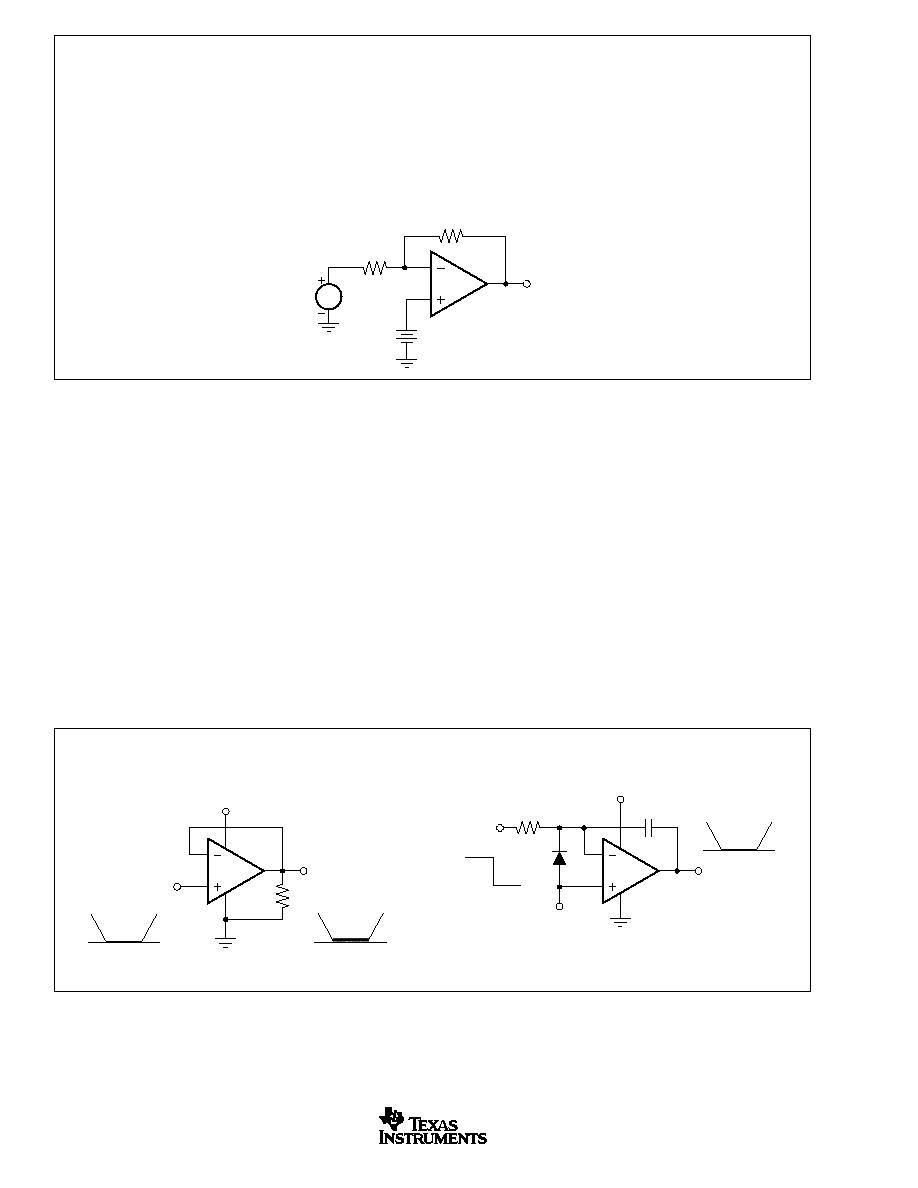
FIGURE 3. Design Optimization.
In most applications, operation is within the range of only one
differential pair. However, some applications can subject the
amplifier to a common-mode signal in the transition region.
Under this condition, the inherent mismatch between the two
differential pairs may lead to degradation of the CMRR and
THD. The unity-gain buffer configuration is the most problem-
atic--it will traverse through the transition region if a sufficiently
DESIGN OPTIMIZATION WITH RAIL-TO-RAIL INPUT OP AMPS
wide input swing is required. A design option would be to
configure the op amp as a unity-gain inverter as shown below
and hold the noninverting input at a set common-mode voltage
outside the transition region. This can be accomplished with a
voltage divider from the supply. The voltage divider should be
designed such that the biasing point for the noninverting input
is outside the transition region.
COMMON-MODE REJECTION
The CMRR for the OPA349 is specified in two ways so the best
match for a given application may be used. First, the CMRR of
the device in the common-mode range below the transition
region (V
CM
< (V+) ≠ 1.5V) is given. This specification is the
best indicator of the capability of the device when the applica-
tion requires use of one of the differential input pairs. Second,
the CMRR at V
S
= 5V over the entire common-mode range is
specified.
OUTPUT DRIVEN TO V≠ RAIL (DUAL VERSION ONLY)
Loads that connect to single-supply ground (or the V- supply
pin) can cause the OPA2349 (dual version) to oscillate if the
output voltage is driven into the negative rail (Figure 4a).
Similarly, loads that can cause current to flow out of the
output pin when the output voltage is near V≠ can cause
oscillations. The op amp will recover to normal operation a
few microseconds after the output is driven positively out of
the rail.
Some op amp applications can produce this condition even
without a load connected to V≠. The integrator in Figure 4b
shows an example. Assume that the output ramps nega-
tively, and saturates near 0V. Any negative-going step at V
IN
will produce a positive output current pulse through R
1
and
C
1
. This may incite the oscillation. Diode, D
1
, prevents the
input step from pulling output current when the output is
saturated at the rail, thus preventing the oscillation.
FIGURE 4. Output Driven to Negative Rail (Dual Version Only).
V
O
V
IN
V+
OPA2349
0V
a)
b)
R
L
1V
(No Load)
V
IN
V+
2V
0V
OPA2349
0V
C
1
1nF
R
1
1M
D1
1N4148
OPA349, 2349
11
SBOS121A
www.ti.com
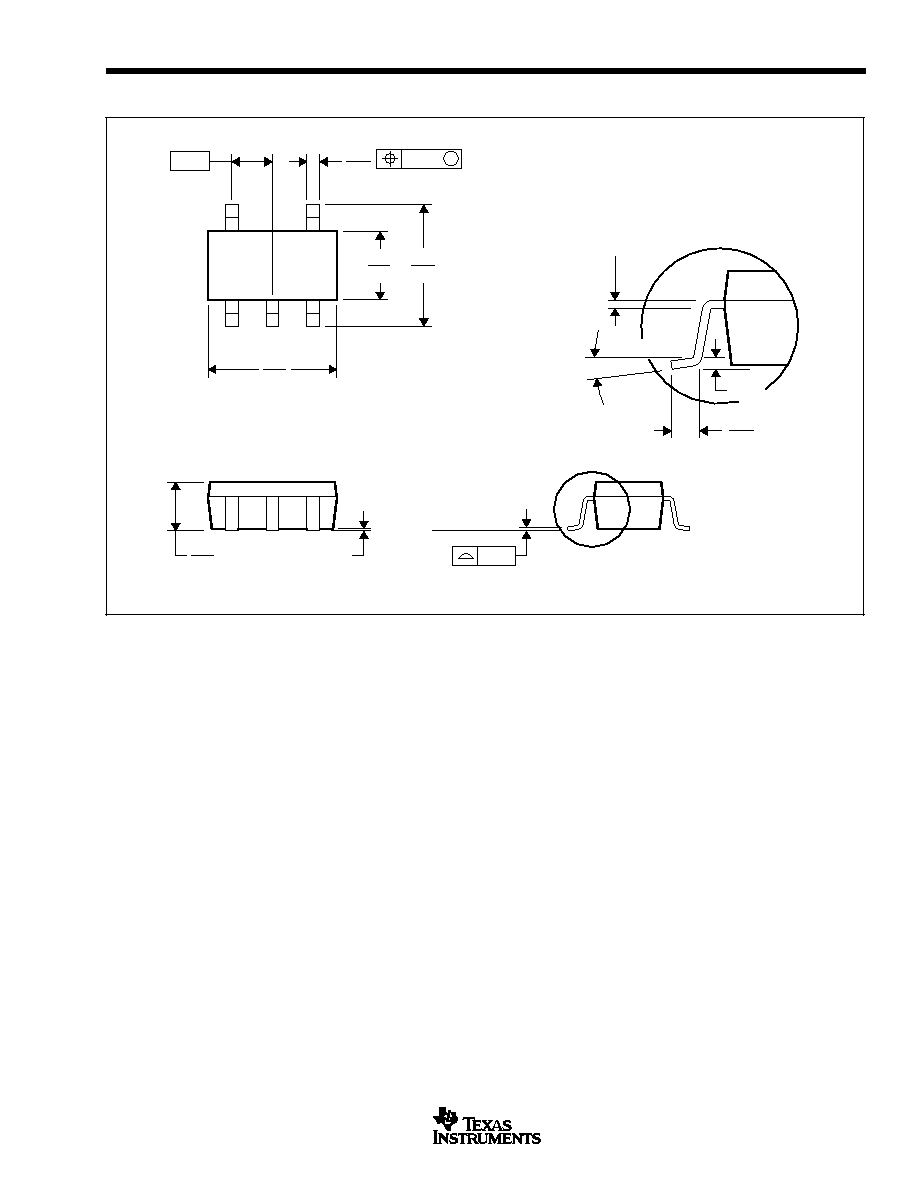
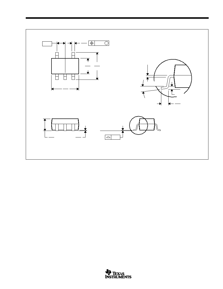
PACKAGE DRAWINGS
MPDS018D ≠ FEBRUARY 1996 ≠ REVISED JANUARY 2001
DBV (R-PDSO-G5)
PLASTIC SMALL-OUTLINE
0,10
M
0,20
0,95
0
∞
≠8
∞
0,25
0,35
0,55
Gage Plane
0,15 NOM
4073253-4/F 10/00
2,60
3,00
0,50
0,30
1,50
1,70
4
5
3
1
2,80
3,00
0,95
1,45
0,05 MIN
Seating Plane
NOTES: A. All linear dimensions are in millimeters.
B. This drawing is subject to change without notice.
C. Body dimensions do not include mold flash or protrusion.
D. Falls within JEDEC MO-178

OPA349, 2349
12
SBOS121A
www.ti.com
PACKAGE DRAWINGS (Cont.)
MSOI002B ≠ JANUARY 1995 ≠ REVISED SEPTEMBER 2001
D (R-PDSO-G**)
PLASTIC SMALL-OUTLINE PACKAGE
8 PINS SHOWN
8
0.197
(5,00)
A MAX
A MIN
(4,80)
0.189
0.337
(8,55)
(8,75)
0.344
14
0.386
(9,80)
(10,00)
0.394
16
DIM
PINS **
4040047/E 09/01
0.069 (1,75) MAX
Seating Plane
0.004 (0,10)
0.010 (0,25)
0.010 (0,25)
0.016 (0,40)
0.044 (1,12)
0.244 (6,20)
0.228 (5,80)
0.020 (0,51)
0.014 (0,35)
1
4
8
5
0.150 (3,81)
0.157 (4,00)
0.008 (0,20) NOM
0
∞
≠ 8
∞
Gage Plane
A
0.004 (0,10)
0.010 (0,25)
0.050 (1,27)
NOTES: A. All linear dimensions are in inches (millimeters).
B. This drawing is subject to change without notice.
C. Body dimensions do not include mold flash or protrusion, not to exceed 0.006 (0,15).
D. Falls within JEDEC MS-012
OPA349, 2349
13
SBOS121A
www.ti.com
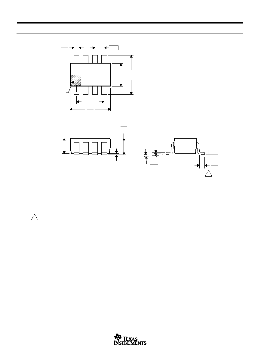
PACKAGE DRAWINGS (Cont.)
MPDS025A ≠ FEBRUARY 1997 ≠ REVISED JUNE 1999
DCK (R-PDSO-G5)
PLASTIC SMALL-OUTLINE
0,10
M
0,10
0,65
0
∞
≠8
∞
0,15
0,46
0,26
Gage Plane
0,13 NOM
4093553/B 06/99
0,15
0,30
1,40
1,10
2,30
1,90
4
5
2,15
1,85
1
3
1,10
0,80
0,10
0,00
Seating Plane
NOTES: A. All linear dimensions are in millimeters.
B. This drawing is subject to change without notice.
C. Body dimensions do not include mold flash or protrusion.
D. Falls within JEDEC MO-203
OPA349, 2349
14
SBOS121A
www.ti.com
PACKAGE DRAWINGS (Cont.)
MPDS099 ≠ MARCH 2001
DCN (R-PDSO-G8)
PLASTIC SMALL-OUTLINE
C
4202106/A 03/01
3,00
2,80
3,00
2,60
1,50
1,75
Area
0,28
0,45
0
∞
≠10
∞
0,09
0,20
1,30
0,90
0,10
0,60
Index
0,00
0,15
≠A≠
0,65
0,90
1,45
1,95 REF
NOTES: A. All linear dimensions are in millimeters.
B. This drawing is subject to change without notice.
C. Foot length measured reference to flat foot surface
parallel to Datum A.
D. Package outline exclusive of mold flash, metal burr and
dambar protrusion/intrusion.
E. Package outline inclusive of solder plating.
F. A visual index feature must be located within the
cross-hatched area.
PACKAGING INFORMATION
ORDERABLE DEVICE
STATUS(1)
PACKAGE TYPE
PACKAGE DRAWING
PINS
PACKAGE QTY
OPA2349EA/250
ACTIVE
SSOP
DCN
8
250
OPA2349EA/3K
ACTIVE
SSOP
DCN
8
3000
OPA2349UA
ACTIVE
SOIC
D
8
100
OPA2349UA/2K5
ACTIVE
SOIC
D
8
2500
OPA349NA/250
ACTIVE
SOP
DBV
5
250
OPA349NA/3K
ACTIVE
SOP
DBV
5
3000
OPA349SA/250
ACTIVE
SOP
DCK
5
250
OPA349SA/3K
ACTIVE
SOP
DCK
5
3000
OPA349UA
ACTIVE
SOIC
D
8
100
OPA349UA/2K5
ACTIVE
SOIC
D
8
2500
(1) The marketing status values are defined as follows:
ACTIVE: Product device recommended for new designs.
LIFEBUY: TI has announced that the device will be discontinued, and a lifetime-buy period is in effect.
NRND: Not recommended for new designs. Device is in production to support existing customers, but TI does not recommend using this part in
a new design.
PREVIEW: Device has been announced but is not in production. Samples may or may not be available.
OBSOLETE: TI has discontinued the production of the device.
PACKAGE OPTION ADDENDUM
www.ti.com
31-Oct-2003

IMPORTANT NOTICE
Texas Instruments Incorporated and its subsidiaries (TI) reserve the right to make corrections, modifications,
enhancements, improvements, and other changes to its products and services at any time and to discontinue
any product or service without notice. Customers should obtain the latest relevant information before placing
orders and should verify that such information is current and complete. All products are sold subject to TI's terms
and conditions of sale supplied at the time of order acknowledgment.
TI warrants performance of its hardware products to the specifications applicable at the time of sale in
accordance with TI's standard warranty. Testing and other quality control techniques are used to the extent TI
deems necessary to support this warranty. Except where mandated by government requirements, testing of all
parameters of each product is not necessarily performed.
TI assumes no liability for applications assistance or customer product design. Customers are responsible for
their products and applications using TI components. To minimize the risks associated with customer products
and applications, customers should provide adequate design and operating safeguards.
TI does not warrant or represent that any license, either express or implied, is granted under any TI patent right,
copyright, mask work right, or other TI intellectual property right relating to any combination, machine, or process
in which TI products or services are used. Information published by TI regarding third-party products or services
does not constitute a license from TI to use such products or services or a warranty or endorsement thereof.
Use of such information may require a license from a third party under the patents or other intellectual property
of the third party, or a license from TI under the patents or other intellectual property of TI.
Reproduction of information in TI data books or data sheets is permissible only if reproduction is without
alteration and is accompanied by all associated warranties, conditions, limitations, and notices. Reproduction
of this information with alteration is an unfair and deceptive business practice. TI is not responsible or liable for
such altered documentation.
Resale of TI products or services with statements different from or beyond the parameters stated by TI for that
product or service voids all express and any implied warranties for the associated TI product or service and
is an unfair and deceptive business practice. TI is not responsible or liable for any such statements.
Following are URLs where you can obtain information on other Texas Instruments products and application
solutions:
Products
Applications
Amplifiers
amplifier.ti.com
Audio
www.ti.com/audio
Data Converters
dataconverter.ti.com
Automotive
www.ti.com/automotive
DSP
dsp.ti.com
Broadband
www.ti.com/broadband
Interface
interface.ti.com
Digital Control
www.ti.com/digitalcontrol
Logic
logic.ti.com
Military
www.ti.com/military
Power Mgmt
power.ti.com
Optical Networking
www.ti.com/opticalnetwork
Microcontrollers
microcontroller.ti.com
Security
www.ti.com/security
Telephony
www.ti.com/telephony
Video & Imaging
www.ti.com/video
Wireless
www.ti.com/wireless
Mailing Address:
Texas Instruments
Post Office Box 655303 Dallas, Texas 75265
Copyright
2003, Texas Instruments Incorporated