26
23
20
17
14
11
8
5
Frequency (Hz)
0.1M
1M
10M
100M
1G
f
≠3dB
DIFFERENTIAL TO SINGLE-ENDED
FREQUENCY RESPONSE
Gain (dB)
Triple Wideband, Current-Feedback
OPERATIONAL AMPLIFIER With Disable
OPA3681
FEATURES
q
WIDEBAND +5V OPERATION: 225MHz (G = +2)
q
UNITY GAIN STABLE: 280MHz (G = 1)
q
HIGH OUTPUT CURRENT: 150mA
q
OUTPUT VOLTAGE SWING:
±
4.0V
q
HIGH SLEW RATE: 2100V/
µ
s
q
LOW SUPPLY CURRENT: 6mA/ch
q
LOW DISABLED CURRENT: 300
µ
A/ch
q
IMPROVED HIGH FREQUENCY PINOUT
APPLICATIONS
q
RGB AMPLIFIERS
q
WIDEBAND INA
q
BROADBAND VIDEO BUFFERS
q
HIGH SPEED IMAGING CHANNELS
q
PORTABLE INSTRUMENTS
q
ADC BUFFERS
q
ACTIVE FILTERS
q
CABLE DRIVERS
DESCRIPTION
The OPA3681 sets a new level of performance for broadband
triple current-feedback op amps. Operating on a very low
6mA/ch supply current, the OPA3681 offers a slew rate and
output power normally associated with a much higher supply
current. A new output stage architecture delivers a high output
current with minimal voltage headroom and crossover distor-
tion. This gives exceptional single-supply operation. Using a
single +5V supply, the OPA3681 can deliver a 1V to 4V output
swing with over 100mA drive current and 150MHz bandwidth.
This combination of features makes the OPA3681 an ideal RGB
line driver or single-supply ADC input driver.
The OPA3681's low 6mA/ch supply current is precisely trimmed
at 25
∞
C. This trim, along with low drift over temperature,
guarantees lower guaranteed maximum supply current than
competing products. System power may be further reduced by
using the optional disable control pin. Leaving this disable pin
open, or holding it high, gives normal operation. If pulled low,
the OPA3681 supply current drops to less than 300
µ
A/ch while
the output goes into a high impedance state. This feature may be
used for power savings or for video MUX applications.
TM
OPA3681 RELATED PRODUCTS
SINGLES
DUALS
TRIPLES
Voltage Feedback
OPA680
OPA2680
OPA3680
Current Feedback
OPA681
OPA2681
OPA3681
Fixed Gain
OPA682
OPA2682
OPA3682
OPA3681
OPA3681
66.5
High Speed INA (>120MHz)
499
499
301
301
1/3
OPA3681
1/3
OPA3681
1/3
OPA3681
V
1
10 (V
1
≠ V
2
)
V
2
+5
≠5
+5
≠5
+5
≠5
250
250
Copyright © 1999, Texas Instruments Incorporated
SBOS095A
Printed in U.S.A. January, 2001
www.ti.com
OPA3681
2
SBOS095A
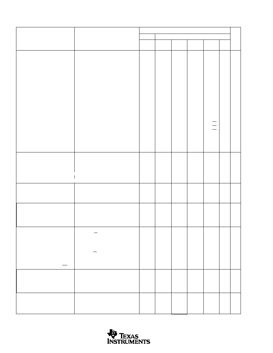
SPECIFICATIONS: V
S
=
±
5V
R
F
= 499
, R
L
= 100
, and G = +2
,
(Figure 1 for AC performance only), unless otherwise noted.
OPA3681E, U
TYP
GUARANTEED
0
∞
C to
≠40
∞
C to
MIN/
TEST
PARAMETER
CONDITIONS
+25
∞
C
+25
∞
C
(2)
70
∞
C
(3)
+85
∞
C
(3)
UNITS
MAX
LEVEL
(1)
AC PERFORMANCE (Figure 1)
Small Signal Bandwidth (V
O
= 0.5Vp-p)
G = +1, R
F
= 549
280
MHz
typ
C
G = +2, R
F
= 499
220
220
210
190
MHz
min
B
G = +5, R
F
= 365
185
MHz
typ
C
G = +10, R
F
= 182
125
MHz
typ
C
Bandwidth for 0.1dB Gain Flatness
G = +2, V
O
= 0.5Vp-p
90
50
45
45
MHz
min
B
Peaking at a Gain of +1
R
F
= 453, V
O
= 0.5Vp-p
0.4
2
4
dB
max
B
Large Signal Bandwidth
G = +2, V
O
= 5Vp-p
150
MHz
typ
C
Slew Rate
G = +2, 4V Step
2100
1600
1600
1200
V/
µ
s
min
B
Rise/Fall Time
G = +2, V
O
= 0.5V Step
1.7
ns
typ
C
G = +2, 5V Step
2.0
ns
typ
C
Settling Time to 0.02%
G = +2, V
O
= 2V Step
12
ns
typ
C
0.1%
G = +2, V
O
= 2V Step
8
ns
typ
C
Harmonic Distortion
G = +2, f = 5MHz, V
O
= 2Vp-p
2nd Harmonic
R
L
= 100
≠75
dBc
typ
C
R
L
500
≠81
dBc
typ
C
3rd Harmonic
R
L
= 100
≠80
dBc
typ
C
R
L
500
≠95
dBc
typ
C
Input Voltage Noise
f > 1MHz
2.2
3.0
3.4
3.6
nV/
Hz
max
B
Non-Inverting Input Current Noise
f > 1MHz
12
14
15
15
pA/
Hz
max
B
Inverting Input Current Noise
f > 1MHz
15
18
18
19
pA/
Hz
max
B
Differential Gain
G = +2, NTSC, V
O
= 1.4Vp, R
L
= 150
0.001
%
typ
C
R
L
= 37.5
0.005
%
typ
C
Differential Phase
G = +2, NTSC, V
O
= 1.4Vp, R
L
= 150
0.01
deg
typ
C
R
L
= 37.5
0.05
deg
typ
C
Crosstalk
Input Referred, f = 5MHz, All Hostile
≠55
dBc
typ
C
DC PERFORMANCE
(4)
Open-Loop Transimpedance Gain (Z
OL
)
V
O
= 0V, R
L
= 100
100
56
56
56
k
min
A
Input Offset Voltage
V
CM
= 0V
±
1.3
±
5
±
6.5
±
7.5
mV
max
A
Average Offset Voltage Drift
V
CM
= 0V
+35
+40
µ
V/
∞
C
max
B
Non-Inverting Input Bias Current
V
CM
= 0V
+30
+55
±
65
±
85
µ
A
max
A
Average Non-Inverting Input Bias Current Drift
V
CM
= 0V
≠400
≠450
nA/
∞
C
max
B
Inverting Input Bias Current
V
CM
= 0V
±
10
±
40
±
50
±
55
µ
A
max
A
Average Inverting Input Bias Current Drift
V
CM
= 0V
≠125
≠150
nA
∞
/C
max
B
INPUT
Common-Mode Input Range
(5)
±
3.5
±
3.4
±
3.3
±
3.2
V
min
A
Common-Mode Rejection (CMR)
V
CM
= 0V
52
47
46
45
dB
min
A
Non-Inverting Input Impedance
100 || 2
k
|| pF
typ
C
Inverting Input Resistance (R
I
)
Open Loop
42
typ
C
OUTPUT
Voltage Output Swing
No Load
±
4.0
±
3.8
±
3.7
±
3.6
V
min
A
R
L
= 100
±
3.9
±
3.7
±
3.6
±
3.3
V
min
A
Current Output, Sourcing
V
O
= 0
+190
+160
+140
+80
mA
min
A
Current Output, Sinking
V
O
= 0
≠150
≠135
≠130
≠80
mA
min
A
Closed-Loop Output Impedance
G = +2, f = 100kHz
0.03
typ
C
DISABLE (Disabled Low)
Power Down Supply Current (+V
S
)
V
DIS
= 0, All Channels
≠960
µ
A
typ
C
Disable Time
100
ns
typ
C
Enable Time
25
ns
typ
C
Off Isolation
G = +2, 5MHz
70
dB
typ
C
Output Capacitance in Disable
4
pF
typ
C
Turn On Glitch
G = +2, R
L
= 150
, V
IN
= 0
±
50
mV
typ
C
Turn Off Glitch
G = +2, R
L
= 150
, V
IN
= 0
±
20
mV
typ
C
Enable Voltage
3.3
3.5
3.6
3.7
V
min
A
Disable Voltage
1.8
1.7
1.6
1.5
V
max
A
Control Pin Input Bias Current (DIS)
V
DIS
= 0, Each Channel
100
160
160
160
µ
A
max
A
POWER SUPPLY
Specified Operating Voltage
±
5
V
typ
C
Maximum Operating Voltage Range
±
6
±
6
±
6
V
max
A
Max Quiescent Current (3 Channels)
V
S
=
±
5V
18
19.2
19.5
19.8
mA
max
A
Min Quiescent Current (3 Channels)
V
S
=
±
5V
18
16.8
16.5
15.0
mA
min
A
Power Supply Rejection Ratio (≠PSRR)
Input Referred
58
52
50
49
dB
min
A
TEMPERATURE RANGE
Specification: E, U
≠40 to +85
∞
C
typ
C
Thermal Resistance,
JA
E
SSOP-16
100
∞
C/W
typ
C
U
SO-16
100
∞
C/W
typ
C
NOTES: (1) Test Levels: (A) 100% tested at 25
∞
C. Over temperature limits by characterization and simulation. (B) Limits set by characterization and simulation.
(C) Typical value only for information. (2) Junction temperature = ambient for 25
∞
C guaranteed specifications. (3) Junction temperature = ambient at low temperature
limit: Junction temperature = ambient +23
∞
C at high temperature limit for over temperature guaranteed specifications. (4) Current is considered positive out of node.
V
CM
is the input common-mode voltage. (5) Tested < 3dB below minimum specified CMR at
±
CMIR limits.
3
OPA3681
SBOS095A
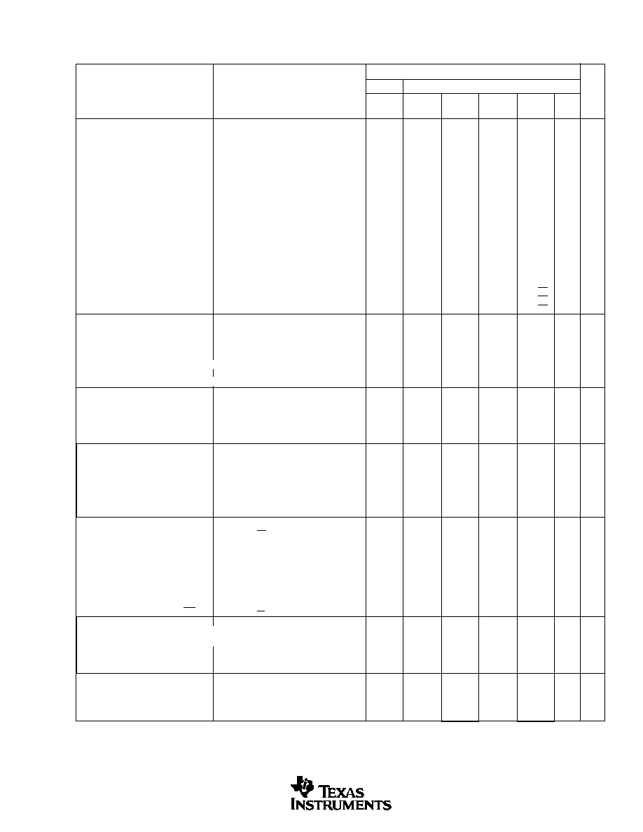
SPECIFICATIONS: V
S
= +5V
R
F
= 499
, R
L
= 100
to V
S
/2, G = +2
,
(Figure 2 for AC performance only), unless otherwise noted.
OPA3681E, U
TYP
GUARANTEED
0
∞
C to
≠40
∞
C to
MIN/
TEST
PARAMETER
CONDITIONS
+25
∞
C
+25
∞
C
(2)
70
∞
C
(3)
+85
∞
C
(3)
UNITS
MAX
LEVEL
(1)
AC PERFORMANCE (Figure 2)
Small Signal Bandwidth (V
O
= 0.5Vp-p)
G = +1, R
F
= 549
250
MHz
typ
C
G = +2, R
F
= 499
225
180
140
110
MHz
min
B
G = +5, R
F
= 365
180
MHz
typ
C
G = +10, R
F
= 182
165
MHz
typ
C
Bandwidth for 0.1dB Gain Flatness
G = +2, V
O
< 0.5Vp-p
100
50
35
23
MHz
min
B
Peaking at a Gain of +1
R
F
= 649
, V
O
< 0.5Vp-p
0.4
2
4
dB
max
B
Large Signal Bandwidth
G = +2, V
O
= 2Vp-p
200
MHz
typ
C
Slew Rate
G = +2, 2V Step
830
700
680
570
V/
µ
s
min
B
Rise/Fall Time
G = +2, V
O
= 0.5V Step
1.5
ns
typ
C
G = +2, V
O
= 2V Step
2.0
ns
typ
C
Settling Time to 0.02%
G = +2, V
O
= 2V Step
14
ns
typ
C
0.1%
G = +2, V
O
= 2V Step
9
ns
typ
C
Harmonic Distortion
G = +2, f = 5MHz, V
O
= 2Vp-p
2nd Harmonic
R
L
= 100
to V
S
/ 2
≠75
dBc
typ
C
R
L
500
to V
S
/2
≠79
dBc
typ
C
3rd Harmonic
R
L
= 100
to V
S
/ 2
≠68
dBc
typ
C
R
L
500
to V
S
/2
≠70
dBc
typ
C
Input Voltage Noise
f > 1MHz
2.2
3
3.4
3.6
nV/
Hz
max
B
Non-Inverting Input Current Noise
f > 1MHz
12
14
14
15
pA/
Hz
max
B
Inverting Input Current Noise
f > 1MHz
15
18
18
19
pA/
Hz
max
B
DC PERFORMANCE
(4)
Open-Loop Transimpedance Gain (Z
OL
)
V
O
= V
S
/2, R
L
= 100
to V
S
/2
100
60
53
51
k
min
A
Input Offset Voltage
V
CM
= 2.5V
±
1
±
5
±
6.0
±
7
mV
max
A
Average Offset Voltage Drift
V
CM
= 2.5V
+15
+20
µ
V/
∞
C
max
B
Non-Inverting Input Bias Current
V
CM
= 2.5V
+40
+65
+75
+95
µ
A
max
A
Average Non-Inverting Input Bias Current Drift
V
CM
= 2.5V
≠300
≠350
nA/
∞
C
max
B
Inverting Input Bias Current
V
CM
= 2.5V
±
5
±
20
±
25
±
35
µ
A
max
A
Average Inverting Input Bias Current Drift
V
CM
= 2.5V
≠125
≠175
nA /
∞
C
max
B
INPUT
Least Positive Input Voltage
(5)
1.5
1.6
1.7
1.8
V
max
A
Most Positive Input Voltage
(5)
3.5
3.4
3.3
3.2
V
min
A
Common-Mode Rejection (CMR)
V
CM
= V
S
/2
51
45
44
44
dB
min
A
Non-Inverting Input Impedance
100 || 2
k
|| pF
typ
C
Inverting Input Resistance (R
I
)
Open Loop
44
typ
C
OUTPUT
Most Positive Output Voltage
No Load
4
3.8
3.7
3.5
V
min
A
R
L
= 100
, 2.5V
3.9
3.7
3.6
3.4
V
min
A
Least Positive Output Voltage
No Load
1
1.2
1.3
1.5
V
max
A
R
L
= 100
, 2.5V
1.1
1.3
1.4
1.6
V
max
A
Current Output, Sourcing
V
O
= V
S
/2
150
110
110
60
mA
min
A
Current Output, Sinking
V
O
= V
S
/2
≠110
≠75
≠70
≠50
mA
min
A
Closed-Loop Output Impedance
G = +2, f = 100kHz
0.03
typ
C
DISABLE (Disable Low)
Power Down Supply Current (+V
S
)
V
DIS
= 0, All Channels
≠810
µ
A
typ
C
Disable Time
100
ns
typ
C
Enable Time
25
ns
typ
C
Off Isolation
G = +2, 5MHz
65
dB
typ
C
Output Capacitance in Disable
4
pF
typ
C
Turn On Glitch
G = +2, R
L
= 150
, V
IN
= V
S
/2
±
50
mV
typ
C
Turn Off Glitch
G = +2, R
L
= 150
, V
IN
= V
S
/2
±
20
mV
typ
C
Enable Voltage
3.3
3.5
3.6
3.7
V
min
A
Disable Voltage
1.8
1.7
1.6
1.5
V
max
A
Control Pin Input Bias Current (DIS)
V
DIS
= 0, Each Channel
100
µ
A
typ
C
POWER SUPPLY
Specified Single Supply Operating Voltage
5
V
typ
C
Maximum Single Supply Operating Voltage
12
12
12
V
max
A
Max Quiescent Current (3 Channels)
V
S
= +5V
14.4
16.2
16.5
16.5
mA
max
A
Min Quiescent Current (3 Channels)
V
S
= +5V
14.4
12.3
11.1
10.8
mA
min
A
Power Supply Rejection Ratio (+PSRR)
Input Referred
48
dB
typ
C
TEMPERATURE RANGE
Specification: E, U
≠40 to +85
∞
C
typ
C
Thermal Resistance,
JA
E
SSOP-16
100
∞
C/W
typ
C
U
SO-16
100
∞
C/W
typ
C
NOTES: (1) Test Levels: (A) 100% tested at 25
∞
C. Over temperature limits by characterization and simulation. (B) Limits set by characterization and simulation.
(C) Typical value only for information. (2) Junction temperature = ambient for 25
∞
C guaranteed specifications. (3) Junction temperature = ambient at low temperature
limit: Junction temperature = ambient +23
∞
C at high temperature limit for over temperature guaranteed specifications. (4) Current is considered positive out of node.
V
CM
is the input common-mode voltage. (5) Tested < 3dB below minimum specified CMR at
±
CMIR limits.
OPA3681
4
SBOS095A
Power Supply ..............................................................................
±
6.5VDC
Internal Power Dissipation
(1)
............................ See Thermal Information
Differential Input Voltage ..................................................................
±
1.2V
Input Voltage Range ............................................................................
±
V
S
Storage Temperature Range: E, U ................................ ≠40
∞
C to +125
∞
C
Lead Temperature (soldering, 10s) .............................................. +300
∞
C
Junction Temperature (T
J
) ........................................................... +175
∞
C
NOTE:: (1) Packages must be derated based on specified
JA
. Maximum T
J
must be observed.
ABSOLUTE MAXIMUM RATINGS
ELECTROSTATIC
DISCHARGE SENSITIVITY
Electrostatic discharge can cause damage ranging from perfor-
mance degradation to complete device failure. Burr-Brown Corpo-
ration recommends that all integrated circuits be handled and stored
using appropriate ESD protection methods.
ESD damage can range from subtle performance degradation to
complete device failure. Precision integrated circuits may be more
susceptible to damage because very small parametric changes
could cause the device not to meet published specifications.
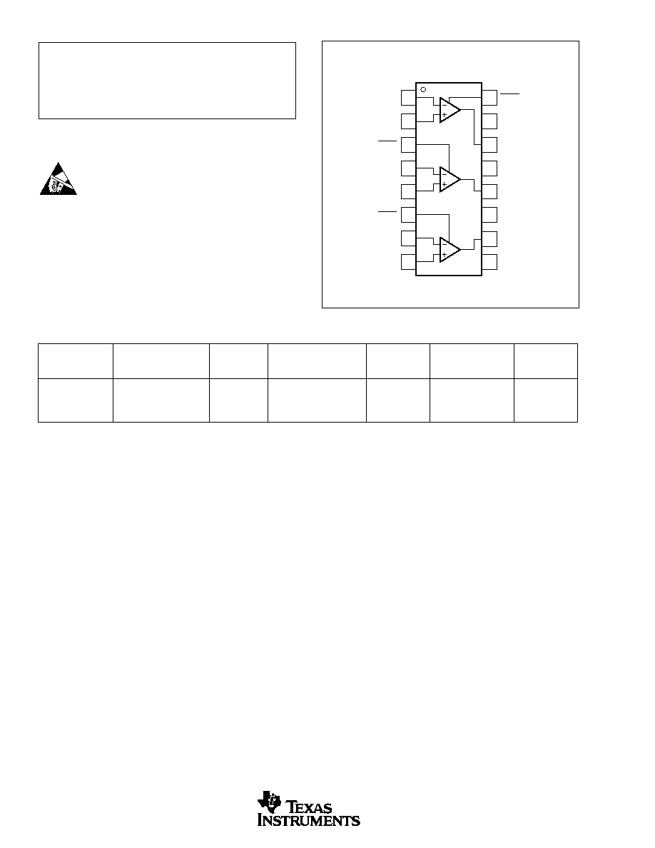
PIN CONFIGURATION
Top View
SSOP-16 , SO-16
PACKAGE
SPECIFIED
DRAWING
TEMPERATURE
PACKAGE
ORDERING
TRANSPORT
PRODUCT
PACKAGE
NUMBER
(1)
RANGE
MARKING
NUMBER
(2)
MEDIA
OPA3681E
SSOP-16 Surface Mount
322
≠40
∞
C to +85
∞
C
OPA3681E
OPA3681E/250
Tape and Reel
"
"
"
"
"
OPA3681E/2K5
Tape and Reel
OPA3681U
SO-16 Surface Mount
265
≠40
∞
C to +85
∞
C
OPA3681U
OPA3681U
Rails
"
"
"
"
"
OPA3681U/2K5
Tape and Reel
NOTES: (1) For detailed drawing and dimension table, please see end of data sheet. (2) Models with a slash (/) are available only in Tape and Reel in the quantities
indicated (e.g., /2K5 indicates 2500 devices per reel). Ordering 2500 pieces of "OPA3681E/2K5" will get a single 2500-piece Tape and Reel.
PACKAGE/ORDERING INFORMATION
1
2
3
4
5
6
7
8
16
15
14
13
12
11
10
9
≠IN A
+IN A
DIS B
≠IN B
+IN B
DIS C
≠IN C
+IN C
DIS A
+V
S
OUT A
≠V
S
OUT B
+V
S
OUT C
≠V
S
OPA3681
5
OPA3681
SBOS095A
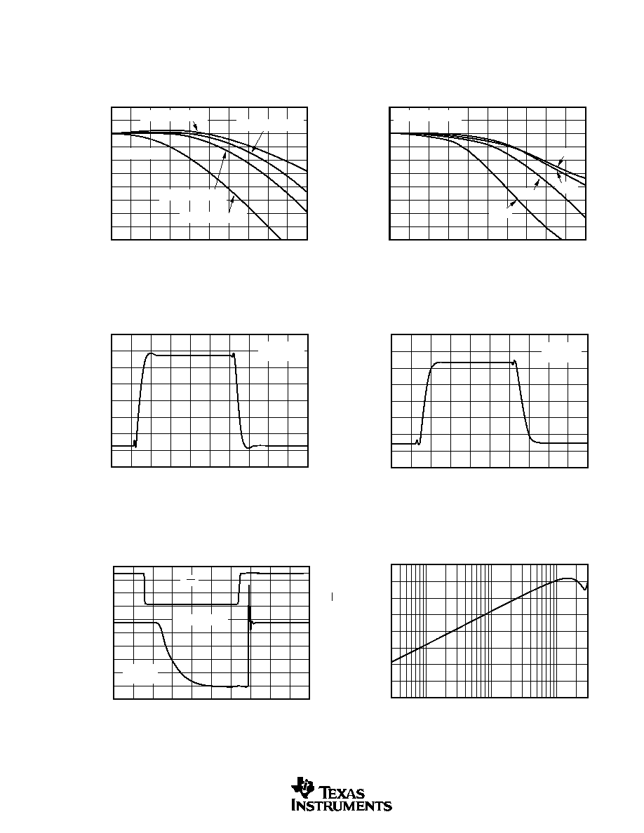
TYPICAL PERFORMANCE CURVES: V
S
=
±
5V
G = +2, R
F
= 499
, and R
L
= 100
, unless otherwise noted (see Figure 1).
2
1
0
≠1
≠2
≠3
≠4
≠5
≠6
≠7
≠8
Frequency (25MHz/div)
0
250MHz
125MHz
SMALL-SIGNAL FREQUENCY RESPONSE
Normalized Gain (1dB/div)
G = +10, R
F
= 182
G = +5, R
F
= 365
G = +1, R
F
= 549
V
O
= 0.5Vp-p
G = +2, R
F
= 499
8
7
6
5
4
3
2
1
0
≠1
≠2
Frequency (25MHz/div)
0
250MHz
125MHz
LARGE-SIGNAL FREQUENCY RESPONSE
Gain (1dB/div)
2Vp-p
G = +2, R
L
= 100
1Vp-p
4Vp-p
7Vp-p
400
300
200
100
0
≠100
≠200
≠300
≠400
SMALL-SIGNAL PULSE RESPONSE
Time (5ns/div)
Output Voltage (100mV/div)
G = +2
V
O
= 0.5Vp-p
+4
+3
+2
+1
0
≠1
≠2
≠3
≠4
LARGE-SIGNAL PULSE RESPONSE
Time (5ns/div)
Output Voltage (1V/div)
G = +2
V
O
= 5Vp-p
5.0
4.0
2.0
0
2.0
1.6
1.2
0.8
0.4
0
LARGE-SIGNAL DISABLE/ENABLE RESPONSE
Time (50ns/div)
Output Voltage (400mV/div)
6.0
4.0
2.0
0
V
DIS
(2V/div)
V
DIS
Output Voltage
G = +2
V
IN
= +1V
ALL HOSTILE CROSSTALK
≠20
≠30
≠40
≠50
≠60
≠70
≠80
≠90
≠100
Frequency (MHz)
0.3
10
100
1
300
Crosstalk (dB)
OPA3681
6
SBOS095A
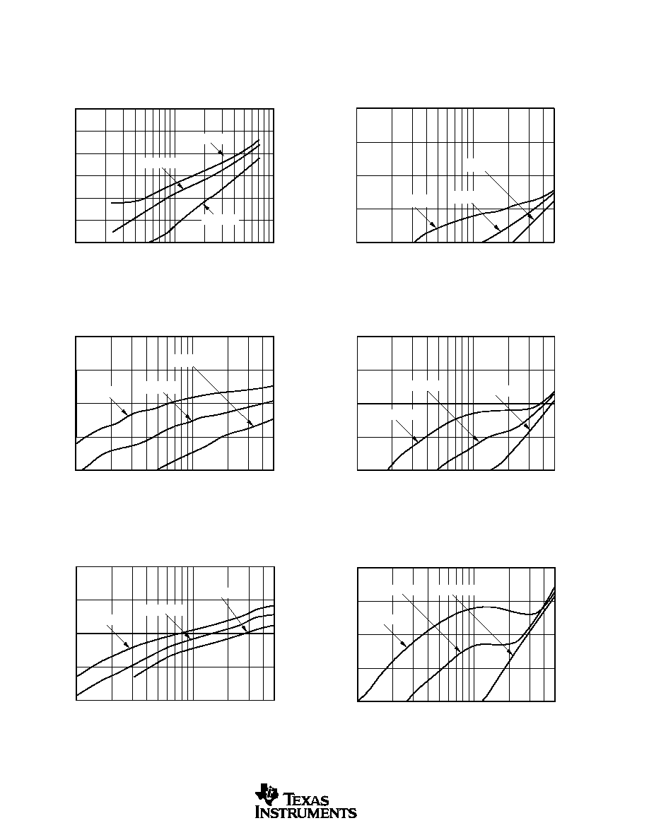
TYPICAL PERFORMANCE CURVES: V
S
=
±
5V
(Cont.)
G = +2, R
F
= 499
, and R
L
= 100
, unless otherwise noted (see Figure 1).
≠60
≠65
≠70
≠75
≠80
≠85
≠90
5MHz 2nd HARMONIC DISTORTION
vs OUTPUT VOLTAGE
Output Voltage Swing (Vp-p)
0.1
1
10
2nd Harmonic Distortion (dBc)
R
L
= 200
R
L
= 500
R
L
= 100
5MHz 3rd HARMONIC DISTORTION
vs OUTPUT VOLTAGE
3rd Harmonic Distortion (dBc)
≠50
≠60
≠70
≠80
≠90
1
0.1
5
Output Voltage (Vp-p)
R
L
= 200
R
L
= 500
R
L
= 100
10MHz 2nd HARMONIC DISTORTION
vs OUTPUT VOLTAGE
2nd Harmonic Distortion (dBc)
≠50
≠60
≠70
≠80
≠90
1
0.1
5
Output Voltage (Vp-p)
R
L
= 200
R
L
= 500
R
L
= 100
10MHz 3rd HARMONIC DISTORTION
vs OUTPUT VOLTAGE
3rd Harmonic Distortion (dBc)
≠50
≠60
≠70
≠80
≠90
1
0.1
5
Output Voltage (Vp-p)
R
L
= 200
R
L
= 500
R
L
= 100
20MHz 2nd HARMONIC DISTORTION
vs OUTPUT VOLTAGE
2nd Harmonic Distortion (dBc)
≠50
≠60
≠70
≠80
≠90
1
0.1
5
Output Voltage (Vp-p)
R
L
= 200
R
L
= 500
R
L
= 100
20MHz 3rd HARMONIC DISTORTION
vs OUTPUT VOLTAGE
3rd Harmonic Distortion (dBc)
≠50
≠60
≠70
≠80
≠90
1
0.1
5
Output Voltage (Vp-p)
R
L
= 200
R
L
= 500
R
L
= 100

7
OPA3681
SBOS095A
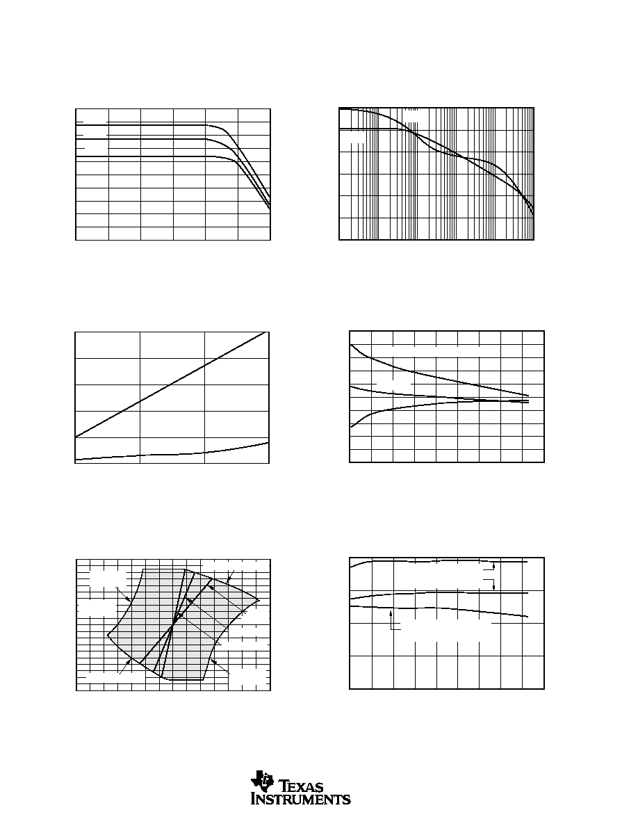
TYPICAL PERFORMANCE CURVES: V
S
=
±
5V
(Cont.)
G = +2, R
F
= 499
, and R
L
= 100
, unless otherwise noted (see Figure 1).
100
10
1
INPUT VOLTAGE AND CURRENT NOISE DENSITY
Frequency (Hz)
100
1k
10k
100k
1M
10M
Current Noise (pA/
Hz)
Voltage Noise (nV/
Hz)
Non-Inverting Input Current Noise
Inverting Input Current Noise
12.2pA/
Hz
15.1pA/
Hz
Voltage Noise
2.2nV/
Hz
≠40
≠45
≠50
≠55
≠60
≠65
≠70
≠75
≠80
≠85
≠90
TWO-TONE, 3RD-ORDER
INTERMODULATION SPURIOUS
Single-Tone Load Power (dBm)
≠8
≠6
≠4
≠2
0
2
4
6
8
10
3rd-Order Spurious Level (dBc)
dBc = dB below carriers
50MHz
20MHz
10MHz
Load Power at Matched 50
Load
60
50
40
30
20
10
0
RECOMMENDED R
S
vs CAPACITIVE LOAD
Capacitive Load (pF)
1
10
100
R
S
(
)
15
12
9
6
3
0
≠3
≠6
≠9
≠12
≠15
Frequency (30MHz/div)
0
300MHz
150MHz
FREQUENCY RESPONSE vs CAPACITIVE LOAD
Gain to Capacitive Load (3dB/div)
R
S
V
IN
V
O
C
L
1k
499
499
1k
is optional.
C
L
= 22pF
C
L
= 10pF
C
L
= 47pF
C
L
= 100pF
3rd HARMONIC DISTORTION
vs FREQUENCY
3rd Harmonic Distortion (dBc)
≠50
≠60
≠70
≠80
≠90
10
1
0.1
20
Frequency (MHz)
V
O
= 2Vp-p
R
L
= 100
G = +2, R
F
= 499
G = +5, R
F
= 365
G = +10, R
F
= 182
≠40
≠50
≠60
≠70
≠80
≠90
Frequency (MHz)
0.1
1
10
20
2nd Harmonic Distortion (dBc)
V
O
= 2Vp-p
R
L
= 100
G = +2, R
F
= 402
G = +10, R
F
= 180
G = +5, R
F
= 261
2nd HARMONIC DISTORTION
vs FREQUENCY
OPA3681
8
SBOS095A
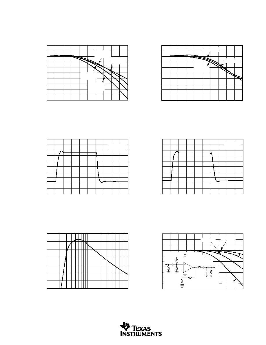
TYPICAL PERFORMANCE CURVES: V
S
=
±
5V
(Cont.)
G = +2, R
F
= 499
, and R
L
= 100
, unless otherwise noted (see Figure 1).
70
65
60
55
50
45
40
35
30
25
20
Frequency (Hz)
10
2
10
3
10
4
10
5
10
6
10
7
10
8
CMR AND PSR vs FREQUENCY
Rejection Ratio (dB)
+PSR
≠PSR
CMR
120
100
80
60
40
20
0
OPEN-LOOP TRANSIMPEDANCE GAIN/PHASE
Frequency (Hz)
10
4
10
5
10
6
10
7
10
8
10
9
Transimpedance Gain (20dB
/div)
0
≠40
≠80
≠120
≠160
≠200
≠240
Transimpedance Phase (40
∞
/div)
| Z
OL
|
Z
OL
0.05
0.04
0.03
0.02
0.01
0
Number of 150
Loads
1
2
3
4
COMPOSITE VIDEO dG/dP
Positive Video
Negative Sync
dP
dG
dG/dP (%/
∞
)
5
4
3
2
1
0
≠1
≠2
≠3
≠4
≠5
TYPICAL DC DRIFT OVER TEMPERATURE
Ambient Temperature (
∞
C)
≠40
≠20
V
IO
0
20
40
60
80
100
120
140
Input Offset Voltage (mV)
50
40
30
20
10
0
≠10
≠20
≠30
≠40
≠50
Input Bias Currents (
µ
A)
Non-Inverting Input Bias Current
Inverting
5
4
3
2
1
0
≠1
≠2
≠3
≠4
≠5
OUTPUT VOLTAGE AND CURRENT LIMITATIONS
I
O
(mA)
≠300
≠200
≠100
0
100
200
300
V
O
(Volts)
100
Load Line
50
Load Line
25
Load Line
Output Current Limited
1W Internal
Power Limit
1-Channel
Only
1W Internal
Power Limit
Output Current Limit
10
7.5
5
2.5
0
200
150
100
50
0
SUPPLY AND OUTPUT CURRENT vs TEMPERATURE
Ambient Temperature (
∞
C)
≠40
≠20
0
20
40
60
80
100
120
140
Supply Current (mA)
Output Current (mA)
Quiescent Supply Current
Sourcing Output Current
Sinking Output Current
9
OPA3681
SBOS095A
TYPICAL PERFORMANCE CURVES: V
S
= +5V
G = +2, R
F
= 499
, and R
L
= 100
, unless otherwise noted (see Figure 1).
2
1
0
≠1
≠2
≠3
≠4
≠5
≠6
≠7
≠8
Frequency (25MHz/div)
0
250
125
SMALL-SIGNAL FREQUENCY RESPONSE
Normalized Gain (1dB/div)
G = +2,
R
F
= 499
V
O
= 0.5Vp-p
G = +10,
R
F
= 182
G = +5,
R
F
= 365
G = +1,
R
F
= 549
8
7
6
5
4
3
2
1
0
≠1
≠2
Frequency (25MHz/div)
0
250
125
LARGE-SIGNAL FREQUENCY RESPONSE
Gain (1dB/div)
G = +2
R
L
= 100
to 2.5V
V
O
= 0.5Vp-p
V
O
= 1Vp-p
V
O
= 2Vp-p
2.10
2.9
2.8
2.7
2.6
2.5
2.4
2.3
2.2
2.1
2.0
SMALL-SIGNAL PULSE RESPONSE
Time (5ns/div)
Output Voltage (100mV/div)
G = +2
V
O
= 0.5Vp-p
4.5
4.1
3.7
3.3
2.9
2.5
2.1
1.7
1.3
0.9
0.5
LARGE-SIGNAL PULSE RESPONSE
Time (5ns/div)
Output Voltage (400mV/div)
G = +2
V
O
= 2Vp-p
70
60
50
40
30
20
10
0
RECOMMENDED R
S
vs CAPACITIVE LOAD
Capacitive Load (pF)
1
10
100
R
S
(
)
15
12
9
6
3
0
≠3
≠6
≠9
≠12
≠15
FREQUENCY RESPONSE vs CAPACITIVE LOAD
Frequency (20MHz/div)
0
200MHz
100MHz
Gain to Capacitive Load (3dB/div)
C
L
= 22pF
C
L
= 10pF
C
L
= 47pF
C
L
= 100pF
499
499
57.6
806
806
1k
V
I
+5V
0.1
µ
F
V
O
R
S
C
L
0.1
µ
F
0.1
µ
F
OPA3681
10
SBOS095A
TYPICAL PERFORMANCE CURVES: V
S
= +5V
(Cont.)
G = +2, R
F
= 499
, and R
L
= 100
, unless otherwise noted (see Figure 1).
10
1
0.1
0.01
CLOSED-LOOP OUTPUT IMPEDANCE
Frequency (Hz)
10k
100M
100k
1M
10M
Output Impedance (
)
499
+5
1/3
OPA3681
≠5
499
50
Z
O
≠45
≠50
≠55
≠60
≠65
≠70
≠75
≠80
≠85
Single-Tone Load Power (dBm)
≠14
≠12
≠10
≠8
≠6
≠4
≠2
0
2
TWO-TONE, 3rd-ORDER SPURIOUS LEVEL
3rd-Order Spurious (dBc)
50MHz
dBc = dB Below Carrier
Load Power at Matched 50
Load
20MHz
10MHz
2nd HARMONIC DISTORTION
vs FREQUENCY
2nd Harmonic Distortion (dBc)
≠50
≠60
≠70
≠80
≠90
10
1
0.1
20
Frequency (MHz)
V
O
= 2Vp-p
R
L
= 100
G = +2, R
F
= 499
G = +5, R
F
= 365
G = +10, R
F
= 182
3rd HARMONIC DISTORTION
vs FREQUENCY
3rd Harmonic Distortion (dBc)
≠50
≠60
≠70
≠80
≠90
10
1
0.1
20
Frequency (MHz)
V
O
= 2Vp-p
R
L
= 100
G = +2, R
F
= 499
G = +5, R
F
= 365
G = +10, R
F
= 182
2nd HARMONIC DISTORTION
vs FREQUENCY
2nd Harmonic Distortion (dBc)
≠50
≠60
≠70
≠80
≠90
10
1
0.1
20
Frequency (MHz)
V
O
= 2Vp-p
G = +2
R
L
= 200
R
L
= 500
R
L
= 100
3rd HARMONIC DISTORTION
vs FREQUENCY
3rd Harmonic Distortion (dBc)
≠50
≠60
≠70
≠80
≠90
10
1
0.1
20
Frequency (MHz)
V
O
= 2Vp-p
G = +2
R
L
= 200
R
L
= 500
R
L
= 100
11
OPA3681
SBOS095A
APPLICATIONS INFORMATION
WIDEBAND CURRENT-FEEDBACK OPERATION
The OPA3681 gives the exceptional AC performance of a
wideband current-feedback op amp with a highly linear,
high power output stage. Requiring only 6mA/ch quiescent
current, the OPA3681 will swing to within 1V of either
supply rail and deliver in excess of 135mA guaranteed at
room temperature. This low output headroom requirement,
along with supply voltage independent biasing, gives re-
markable single (+5V) supply operation. The OPA3681 will
deliver greater than 200MHz bandwidth driving a 2Vp-p
output into 100
on a single +5V supply. Previous boosted
output stage amplifiers have typically suffered from very
poor crossover distortion as the output current goes through
zero. The OPA3681 achieves a comparable power gain with
much better linearity. The primary advantage of a current-
feedback op amp over a voltage-feedback op amp is that AC
performance (bandwidth and distortion) is relatively inde-
pendent of signal gain.
Figure 1 shows the DC-coupled, gain of +2, dual power
supply circuit configuration used as the basis of the
±
5V
Specifications and Typical Performance Curves. For test
purposes, the input impedance is set to 50
with a resistor
to ground and the output impedance is set to 50
with a
series output resistor. Voltage swings reported in the speci-
fications are taken directly at the input and output pins while
load powers (dBm) are defined at a matched 50
load. For
the circuit of Figure 1, the total effective load will be 100
|| 998
. The disable control line (DIS) is typically left open
to guarantee normal amplifier operation. One optional com-
ponent is included in Figure 1. In addition to the usual power
supply de-coupling capacitors to ground, a 0.1
µ
F capacitor
is included between the two power supply pins. In practical
PC board layouts, this optionally added capacitor will typi-
cally improve the 2nd harmonic distortion performance by
3dB to 6dB.
Figure 2 shows the AC-coupled, gain of +2, single-supply
circuit configuration used as the basis of the +5V Specifica-
tions and Typical Performance Curves. Though not a "rail-
to-rail" design, the OPA3681 requires minimal input and
output voltage headroom compared to other very wideband
current-feedback op amps. It will deliver a 3Vp-p output
swing on a single +5V supply with greater than 150MHz
bandwidth. The key requirement of broadband single-supply
operation is to maintain input and output signal swings
within the usable voltage ranges at both the input and the
output. The circuit of Figure 2 establishes an input midpoint
bias using a simple resistive divider from the +5V supply
(two 806
resistors). The input signal is then AC-coupled
into this midpoint voltage bias. The input voltage can swing
to within 1.5V of either supply pin, giving a 2Vp-p input
signal range centered between the supply pins. The input
impedance matching resistor (57.6
) used for testing is
adjusted to give a 50
input match when the parallel
combination of the biasing divider network is included. The
gain resistor (R
G
) is AC-coupled, giving the circuit a DC
gain of +1, which puts the input DC bias voltage (2.5V) on
the output as well. Again, on a single +5V supply, the output
voltage can swing to within 1V of either supply pin while
delivering more than 75mA output current. A demanding
100
load to a midpoint bias is used in this characterization
circuit. The new output stage used in the OPA3681 can
deliver large bipolar output currents into this midpoint load
with minimal crossover distortion, as shown by the +5V
supply, 3rd harmonic distortion plots.
1/3
OPA3681
+5V
+
DIS
≠5V
50
Load
50
50
V
O
V
I
50
Source
R
G
499
R
F
499
+
6.8
µ
F
0.1
µ
F
6.8
µ
F
0.1
µ
F
0.1
µ
F
+V
S
≠V
S
FIGURE 1. DC-Coupled, G = +2, Bipolar Supply, Specifi-
cation and Test Circuit.
FIGURE 2. AC-Coupled, G = +2, Single Supply, Specifica-
tion and Test Circuit.
1/3
OPA3681
+5V
+V
S
DIS
V
S
/2
806
100
V
O
V
I
57.6
806
R
F
499
R
G
499
0.1
µ
F
0.1
µ
F
6.8
µ
F
+
0.1
µ
F
OPA3681
12
SBOS095A
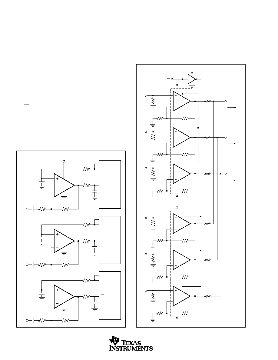
TRIPLE ADC BUFFER CHANNEL
The OPAx681 family is ideally suited to single supply,
wideband ADC driving. A current feedback op amp is ideal
where high gains with high bandwidths are required. The
wide 3Vp-p output swing with over 150MHz full power
bandwidth on a single +5V supply is well suited to the
2Vp-p input range commonly required from modern CMOS
pipelined ADCs. Three channels of very high speed digitizer
channels are shown in Figure 3 using the OPA3681 driving
three ADS831s (8-bit, 80Msps CMOS converters). Each
input is AC-coupled into a 50
gain resistor that also will
act as a 50
impedance match at high frequencies. The
amplifier's inputs and outputs are centered on the ADC
common-mode input voltage by tying each converter's V
CM
to the non-inverting inputs of the amplifier. This V
CM
acts as
the swing midpoint for the input to the converter. Since the
ADS831 can operate with differential inputs, driving into
the IN input will give a net non-inverting signal channel
even with the amplifiers operating at an inverting gain of
≠6. The other input to the ADS831 is tied to this V
CM
as well
to give an input signal midpoint equal to V
CM
. The 300
feedback resistor will be the output load in this configura-
tion. Harmonic distortion for the OPA3681 will not degrade
the converter's SFDR performance in this application.
WIDEBAND RGB MULTIPLEXER
The OPA3681 is ideally suited to implementing a simple,
very wideband, 2x1 RGB multiplexer. This simple "wired-
OR video multiplexer" can be easily implemented using the
circuit shown in Figure 4.
This circuit uses two OPA3681s where each package ac-
cepts the three RGB component video signals from one of
two possible sources. Each non-inverting input is terminated
FIGURE 3. ADC Driver.
FIGURE 4. Wideband 2x1 RGB Multiplexer.
1/3
OPA3681
22
300
50
0.1
µ
F
300
0.1
µ
F
47pF
V
1
ADS831
8-Bit
80Msps
IN
V
CM
IN
1/3
OPA3681
22
300
50
0.1
µ
F
300
0.1
µ
F
47pF
V
1
ADS831
8-Bit
80Msps
IN
V
CM
IN
1/3
OPA3681
22
300
50
0.1
µ
F
300
0.1
µ
F
47pF
V
1
ADS831
8-Bit
80Msps
IN
V
CM
IN
+5V
Power Supply
De-Coupling
Not Shown
1/3
OPA3681
340
402
75
82.5
V
OUT
Red
75
Line
R1
+5V
+5V
≠5V
1/3
OPA3681
340
402
75
82.5
V
OUT
Green
75
Line
G1
1/3
OPA3681
340
402
75
82.5
V
OUT
Blue
75
Line
B1
1/3
OPA3681
340
402
75
82.5
R2
+5V
≠5V
1/3
OPA3681
340
402
75
82.5
G2
1/3
OPA3681
340
402
75
82.5
B2
V
DIS
U1
U2
Power Supply
De-Coupling Not Shown
13
OPA3681
SBOS095A
in 75
to match the typical video source impedance. The
disable control is used to switch between channels by feed-
ing a logic control line directly to all three V
DIS
inputs on
one package, and its complement to the three V
DIS
inputs on
the other. Since the disable feature is intentionally make-
before-break (to ensure that the output does not float in
transition), each of the two possible outputs for the three
RGB lines are combined through a limiting resistor. This
82.5
resistor limits the current between the two outputs
during switching. Each output will have a disabled channel.
The feedback and output network connected on the output
slightly attenuates the signal going out onto the 75
cable.
The gain and output matching resistors (82.5
) have been
slightly increased to get a signal gain of +1 to the matched
load and provide a 75
output impedance to the cable. The
section on Disable Operation shows the turn-on and turn-off
switching glitches, using a grounded input for the single
channel, is typically less than
±
50mV. Where two outputs
are switched (shown in Figure 4), the output line is always
under the control of one amplifier or the other due to the
"make-before-break" disable timing. In this case, the switch-
ing glitches for 0V inputs drops to < 20mV.
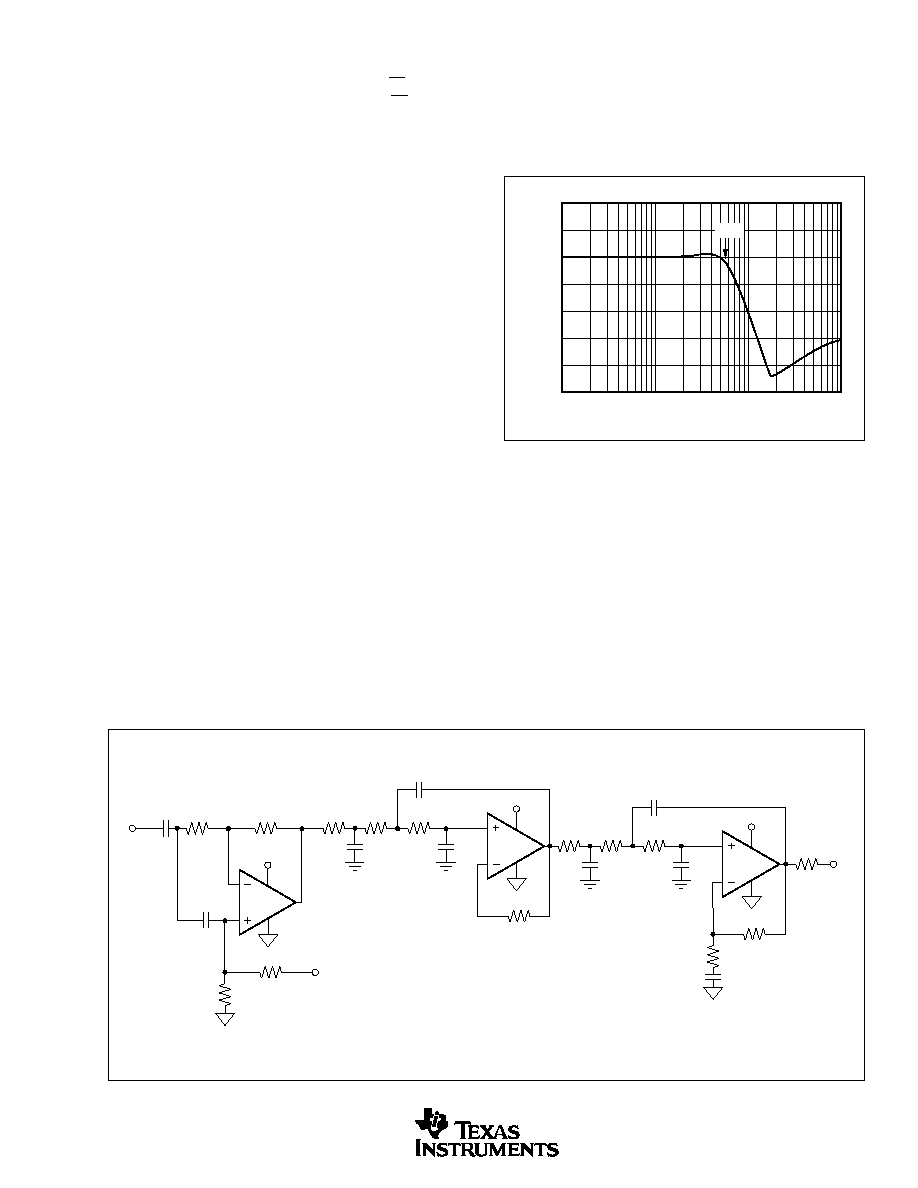
VIDEO DAC RECONSTRUCTION FILTER
Wideband current-feedback op amps make ideal elements
for implementing high-speed active filters where the ampli-
fier is used as fixed gain block inside a passive RC circuit
network. Their relatively constant bandwidth versus gain,
provides low interaction between the actual filter poles and
the required gain for the amplifier. Figure 5 shows an
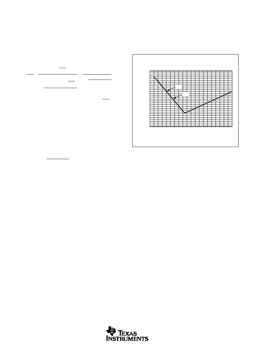
example of a video DAC reconstruction filter.
The delay-equalized filter in Figure 5 compensates for the
DAC's sin(x)/x response, and minimizes aliasing artifacts. It
is designed for single +5V operation, with a 13.5Msps DAC
sampling rate, and a 5.5MHz cutoff frequency.
The first op amp buffers the video DAC output and the first
filter section from each other. This first filter section pro-
vides group delay equalization. The second and third filter
sections provide a 6th-order lowpass filter response that also
compensates for the DAC's sin(x)/x response.
The filter response can be seen in Figure 6.
FIGURE 5. Filter Schematic.
FIGURE 6. DAC Reconstruction Filter Response.
HIGH POWER xDSL LINE DRIVER
Emerging broadband access technologies are making sig-
nificant demands on the output stage drivers. Some of the
higher frequency versions, particularly in VDSL, require
passive bandpass filters to spectrally isolate the upstream
from downstream frequency bands. Figure 7 shows one
possible implementation of this using single-ended filters
and giving differential push/pull drive into a transformer.
The DAC output from the analog front end (AFE) typically
requires isolation from the complex filter impedance. The
first stage provides a tunable gain (using R
G
) with a fixed
412
243
82.5
499
100pF
56pF
220pF
+5V
402
237
97.6
499
1/3
OPA3681
100pF
56pF
220pF
+5V
75.5
1/3
OPA3681
499
100
µ
F
953
+5V
1/3
OPA3681
953
499
499
120pF
100
µ
F
V
O
Video
In
+5V
20
10
0
≠10
≠20
≠30
≠40
≠50
0
1
10
100
Frequency (MHz)
(dB)
f
≠3dB
OPA3681
14
SBOS095A
termination for the DAC, R
T
. It is very useful from a
distortion standpoint to scale the characteristic impedance
up for the filter. This reduces the loading at the first stage
amplifier output, typically improving 3rd-order terms di-
rectly, as well as some improvement in 2nd-order terms.
Figure 7 assumes a 100
characteristic impedance for the
filter. The filter is driven from a 100
source resistor into a
100
load that is formed by the input gain resistor of the
inverting amplifier channel. The other non-inverting input is
isolated by a series 50
resistor--principally to isolate that
input from the out-of-band source impedance of the filter. In
this example, the output stage is set up for a differential gain
of 8. The total gain from the output of the bandpass filter to
the line will be 4 ∑ n, where n is the turns ratio used in the
transformer. Very broad bandwidths at high power levels are
possible using the OPA3681 in the circuit of Figure 7.
Recognize also, that the output is in fact bandlimited by the
filter. Very high dynamic range is possible inside the filter
bandwidth due to the significant performance margin pro-
vided by the OPA3681.
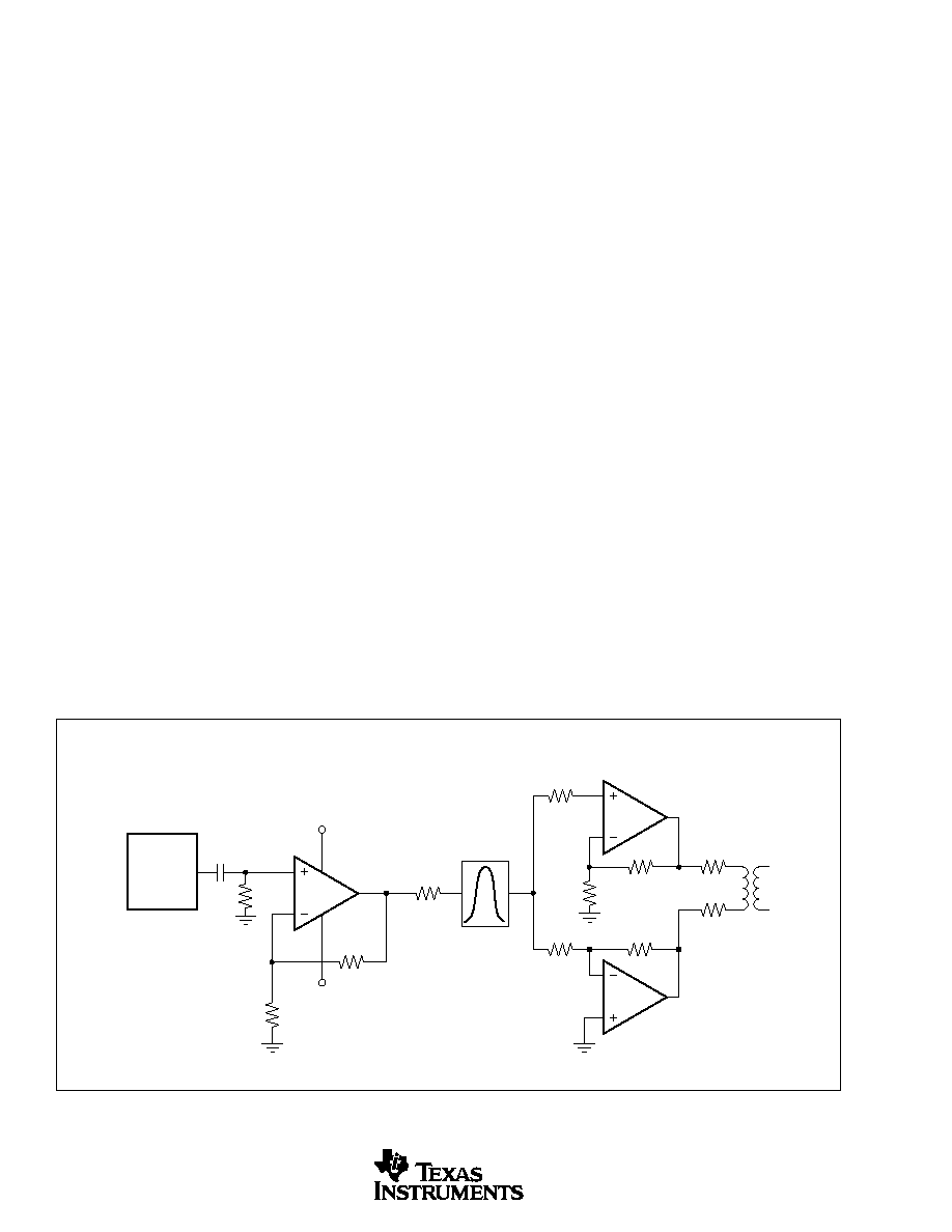
WIDEBAND DIFFERENTIAL AMPLIFIER
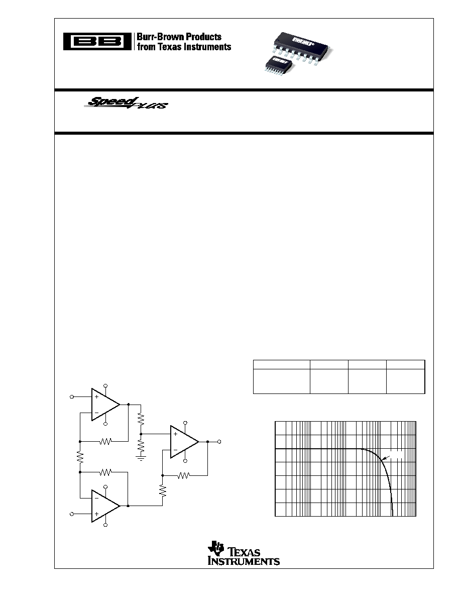
The differential amplifier (three amplifier instrumentation
topology) on the front page of this data sheet shows a
common application applied to this triple current feedback
op amp. The two input stage amplifiers are configured for a
relatively high differential gain of 10. Lowering the feed-
back resistor values in this input stage provides > 120MHz
bandwidth, even at this high gain setting. The signal is
applied to the high impedance, non-inverting inputs at the
input stage. The differential gain is set by (1 + 2R
F
/R
G
) = 10
using the values shown on the front page. The third amplifier
performs the differential-to-single-ended conversion in a
standard single op amp differential stage. This differential
stage, built using the 3rd wideband current-feedback op
amp, in the OPA3681 will give lower CMRR at DC than
using a voltage feedback part, but higher CMRR at higher
frequencies. Measured performance, with no resistor value
tuning, gave approximately 75dB at DC and > 55dB CMRR
(input referred) through 10MHz. To maintain good distor-
tion performance for the input stage amplifiers, the loading
at each output has been matched while achieving the gain of
1 and differential characteristic of the output stage. To
improve DC CMRR, tune the resistor to ground at the non-
inverting input of the output stage amplifier.
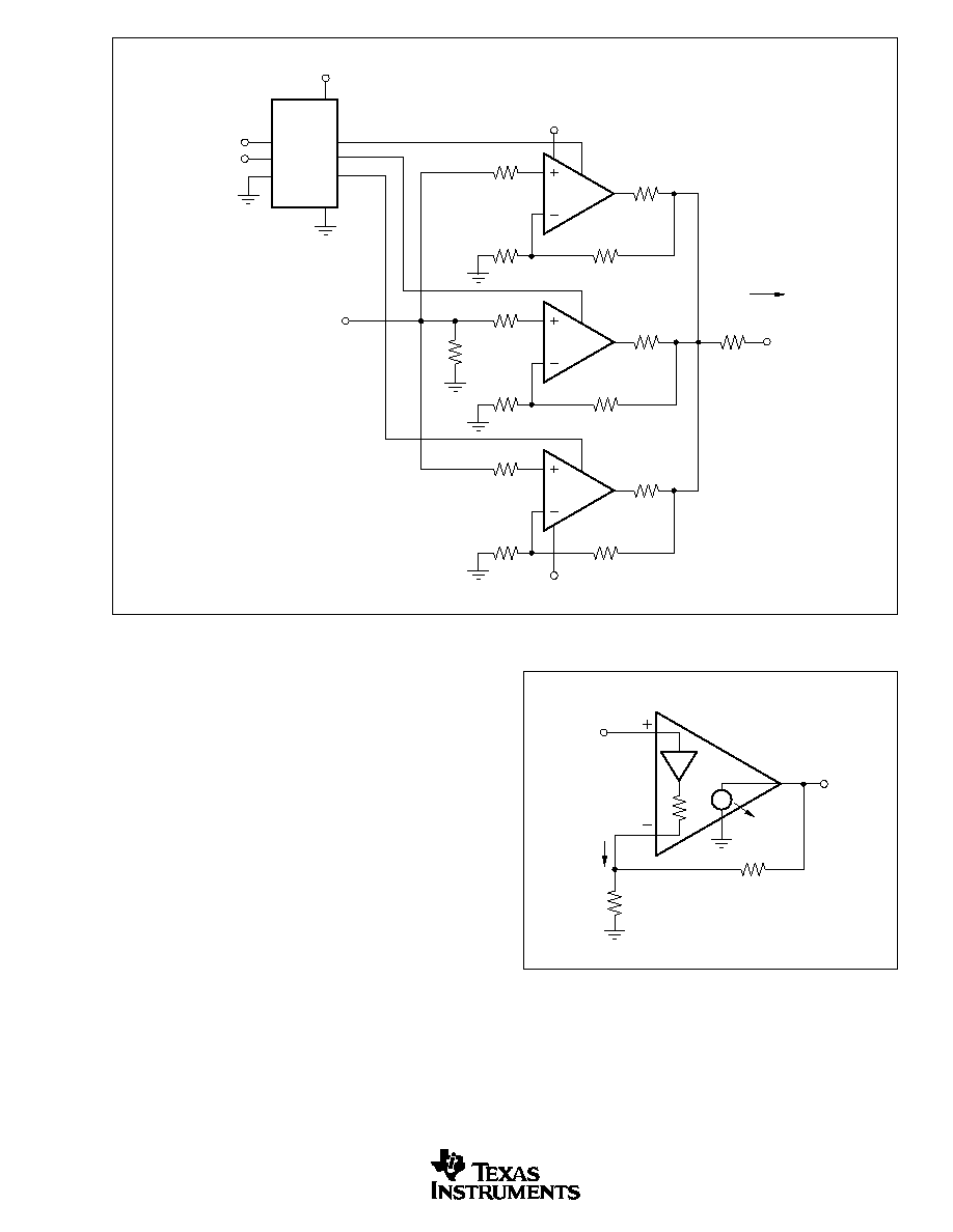
WIDEBAND PROGRAMMABLE GAIN
By tying all three inputs together from a single source, and
all three outputs together to drive a common load, a very
wideband, programmable gain function may be implemented.
Figure 8 shows an example of this application where the
three channels have been set up for gains of 2, 4, and 8 to
their output pins. When driving a doubly-terminated 50
load, this gives a user-selectable gain of 1, 2 and 4 to the
matched load. The feedback resistor value has been opti-
mized for maximum flat bandwidth in each channel. This
will give an almost constant > 200MHz bandwidth at any of
the three gain settings. The desired gain is selected by using
the disable control lines to choose one of the three possible
amplifiers as the active channel. An additional 10
resistor
was included inside the loop on each output stage to limit
output stage currents if more than one output is on during
gain select transition. This will reduce the maximum avail-
able output voltage swing into the 100
total load shown in
Figure 8 to approximately
±
3.2V, but will provide surge
current protection during channel switching. The 20
series
resistors on each non-inverting input serves to isolate the
input parasitic capacitance from the source.
FIGURE 7. Single-to-Differential xDSL Line Driver.
1/3
OPA3681
50
R
S
R
S
1:n
1/3
OPA3681
400
400
100
Bandpass
Filter
133
1/3
OPA3681
100
R
G
R
T
DSL
AFE
400
+5V
≠5V
Supply De-Coupling
Not Shown
15
OPA3681
SBOS095A
OPERATING SUGGESTIONS
SETTING RESISTOR VALUES TO
OPTIMIZE BANDWIDTH
A current-feedback op amp like the OPA3681 can hold an
almost constant bandwidth over signal gain settings with the
proper adjustment of the external resistor values. This is shown
in the Typical Performance Curves; the small signal bandwidth
decreases only slightly with increasing gain. These curves also
show that the feedback resistor has been changed for each gain
setting. The resistor "values" on the inverting side of the circuit
for a current feedback op amp can be treated as frequency
response compensation elements while their "ratios" set the
signal gain. Figure 9 shows the small-signal frequency response
analysis circuit for the OPA3681.
The key elements of this current-feedback op amp model are:
Buffer gain from the non-inverting input to the inverting input
R
I
Buffer output impedance
i
ERR
Feedback error current signal
Z(s)
Frequency dependent open loop transimpedance gain from i
ERR
to V
O
The buffer gain is typically very close to 1.00 and is
normally neglected from signal gain considerations. It will,
however, set the CMRR for a single op amp differential
amplifier configuration. For a buffer gain
< 1.0, the
CMRR = ≠20
∑
log (1≠
) dB.
R
I
, the buffer output impedance, is a critical portion of the
bandwidth control equation. The OPA3681 is typically 42
.
1/3
OPA3681
10
20
499
499
G = +2
1/3
OPA3681
10
20
140
422
G = +4
1/3
OPA3681
10
20
35.7
249
G = +8
74HC238
50
50
Load
≠5V
+5V
Power Supply
De-Coupling Not Shown
V
IN
+5V
D
1
D
2
Y
0
Y
1
Y
2
50
FIGURE 9. Current Feedback Transfer Function Analysis
Circuit.
FIGURE 8. Wideband Programmable Gain.
R
F
V
O
R
G
R
I
Z
(S)
i
ERR
i
ERR
V
I
OPA3681
16
SBOS095A
A current-feedback op amp senses an error current in the
inverting node (as opposed to a differential input error
voltage for a voltage feedback op amp) and passes this on to
the output through an internal frequency dependent
transimpedance gain. The Typical Performance Curves show
this open-loop transimpedance response. This is analogous
to the open-loop voltage gain curve for a voltage-feedback
op amp. Developing the transfer function for the circuit of
Figure 9 gives Equation 1:
This is written in a loop gain analysis format where the
errors arising from a non-infinite open-loop gain are shown
in the denominator. If Z(s) were infinite over all frequencies,
the denominator of Equation 1 would reduce to 1 and the
ideal desired signal gain shown in the numerator would be
achieved. The fraction in the denominator of Equation 1
determines the frequency response. Equation 2 shows this as
the loop gain equation:
If 20
∑
log (R
F
+ NG
∑
R
I
) were drawn on top of the open-
loop transimpedance plot, the difference between the two
would be the loop gain at a given frequency. Eventually,
Z(s) rolls off to equal the denominator of Equation 2 at
which point the loop gain has reduced to 1 (and the curves
have intersected). This point of equality is where the
amplifier's closed-loop frequency response, given by Equa-
tion 1, will start to roll off and is exactly analogous to the
frequency at which the noise gain equals the open-loop
voltage gain for a voltage-feedback op amp. The difference
here is that the total impedance in the denominator of
Equation 2 may be controlled somewhat separately from the
desired signal gain (or NG).
The OPA3681 is internally compensated to give a maxi-
mally flat frequency response for R
F
= 499
at NG = 2 on
±
5V supplies. Evaluating the denominator of Equation 2
(which is the feedback transimpedance) gives an optimal
target of 589
. As the signal gain changes, the contribution
of the NG
∑
R
I
term in the feedback transimpedance will
change, but the total can be held constant by adjusting R
F
.
Equation 3 gives an approximate equation for optimum R
F
over signal gain:
As the desired signal gain increases, this equation will
eventually predict a negative R
F
. A somewhat subjective
limit to this adjustment can also be set by holding R
G
to a
minimum value of 20
. Lower values will load both the
buffer stage at the input and the output stage if R
F
gets too
low--actually decreasing the bandwidth. Figure 10 shows
the recommended R
F
vs NG for both
±
5V and a single +5V
operation. The values shown in Figure 10 give a good
starting point for design where bandwidth optimization is
desired.
The total impedance going into the inverting input may be
used to adjust the closed-loop signal bandwidth. Inserting a
series resistor between the inverting input and the summing
junction will increase the feedback impedance (denominator
of Equation 2), decreasing the bandwidth. The internal
buffer output impedance for the OPA3681 is slightly influ-
enced by the source impedance looking out of the non-
inverting input terminal. High source resistors will have the
effect of increasing R
I
, decreasing the bandwidth. For those
single-supply applications which develop a midpoint bias at
the non-inverting input through high valued resistors, the
decoupling capacitor is essential for power supply ripple
rejection, non-inverting input noise current shunting, and to
minimize the high frequency value for R
I
in Figure 9.
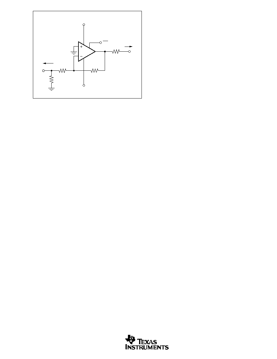
INVERTING AMPLIFIER OPERATION
Since the OPA3681 is a general purpose, wideband current-
feedback op amp, most of the familiar op amp application
circuits are available to the designer. Those triple op amp
applications that require considerable flexibility in the feed-
back element (e.g., integrators, transimpedance, some fil-
ters) should consider the unity gain stable voltage-feedback
OPA2680, since the feedback resistor is the compensation
element for a current feedback op amp. Wideband inverting
operation (especially summing) is particularly suited to the
OPA3681. Figure 11 shows a typical inverting configuration
where the I/O impedances and signal gain from Figure 1 are
retained in an inverting circuit configuration.
600
500
400
300
200
100
0
Noise Gain
0
20
10
15
5
FEEDBACK RESISTOR vs NOISE GAIN
Feedback Resistor (
)
+5V
±
5V
FIGURE 10. Recommended Feedback Resistor vs Noise
Gain.
V
V
R
R
R
R
R
R
Z
NG
R
R NG
Z
O
I
F
G
F
I
F
G
S
F
I
S
=
+
+
+
+
=
+
+
1
1
1
1
( )
( )
NG
R
R
F
G
+
1
Eq. 1
Eq. 2
Z
R
R NG
Loop Gain
S
F
I
( )
+
=
Eq. 3
R
NG R
F
I
=
589
≠
17
OPA3681
SBOS095A
In the inverting configuration, two key design consider-
ations must be noted. The first is that the gain resistor (R
G
)
becomes part of the signal channel input impedance. If input
impedance matching is desired (which is beneficial when-
ever the signal is coupled through a cable, twisted pair, long
PC board trace or other transmission line conductor), it is
normally necessary to add an additional matching resistor to
ground. R
G
by itself is normally not set to the required input
impedance since its value, along with the desired gain, will
determine a R
F
which may be non-optimal from a frequency
response standpoint. The total input impedance for the
source becomes the parallel combination of R
G
and R
M
.
The second major consideration, touched on in the previous
paragraph, is that the signal source impedance becomes part
of the noise gain equation and will have slight effect on the
bandwidth through Equation 1. The values shown in Figure
11 have accounted for this by slightly decreasing R
F
(from
Figure 1) to re-optimize the bandwidth for the noise gain of
Figure 11 (NG = 2.82) In the example of Figure 11, the R
M
value combines in parallel with the external 50
source
impedance, yielding an effective driving impedance of
50
|| 64
= 28.1
. This impedance is added in series with
R
G
for calculating the noise gain--which gives NG = 2.82.
This value, along with the R
F
of Figure 10 and the inverting
input impedance of 45
, are inserted into Equation 3 to get
a feedback transimpedance nearly equal to the 589
opti-
mum value.
Note that the non-inverting input in this bipolar supply
inverting application is connected directly to ground. It is
often suggested that an additional resistor be connected to
ground on the non-inverting input to achieve bias current
error cancellation at the output. The input bias currents for
a current feedback op amp are not generally matched in
either magnitude or polarity. Connecting a resistor to ground
on the non-inverting input of the OPA3681 in the circuit of
Figure 11 will actually provide additional gain for that
input's bias and noise currents, but will not decrease the
output DC error since the input bias currents are not matched.
OUTPUT CURRENT AND VOLTAGE
The OPA3681 provides output voltage and current capabili-
ties that are unsurpassed in a low cost dual monolithic op
amp. Under no-load conditions at 25
∞
C, the output voltage
typically swings closer than 1V to either supply rail; the
guaranteed swing limit is within 1.2V of either rail. Into a
15
load (the minimum tested load), it is guaranteed to
deliver more than
±
135mA.
The specifications described above, though familiar in the
industry, consider voltage and current limits separately. In
many applications, it is the voltage
∑
current, or V-I product,
which is more relevant to circuit operation. Refer to the
"Output Voltage and Current Limitations" plot in the Typi-
cal Performance Curves. The X and Y axes of this graph
show the zero-voltage output current limit and the zero-
current output voltage limit, respectively. The four quad-
rants give a more detailed view of the OPA3681's output
drive capabilities, noting that the graph is bounded by a
"Safe Operating Area" of 1W maximum internal power
dissipation. Superimposing resistor load lines onto the plot
shows that the OPA3681 can drive
±
2.5V into 25
or
±
3.5V
into 50
without exceeding the output capabilities or the
1W dissipation limit. A 100
load line (the standard test
circuit load) shows the full
±
3.9V output swing capability,
as shown in the Specifications Table.
The minimum specified output voltage and current over
temperature are set by worst-case simulations at the cold
temperature extreme. Only at cold startup will the output
current and voltage decrease to the numbers shown in the
guaranteed tables. As the output transistors deliver power,
their junction temperatures will increase, decreasing their
V
BE
's (increasing the available output voltage swing) and
increasing their current gains (increasing the available out-
put current). In steady state operation, the available output
voltage and current will always be greater than that shown
in the over-temperature specifications since the output stage
junction temperatures will be higher than the minimum
specified operating ambient.
To maintain maximum output stage linearity, no output
short-circuit protection is provided. This will not normally
be a problem since most applications include a series match-
ing resistor at the output that will limit the internal power
dissipation if the output side of this resistor is shorted to
ground. However, shorting the output pin directly to the
adjacent positive power supply pins will, in most cases,
destroy the amplifier. If additional short-circuit protection
is required, consider a small series resistor in the power
supply leads. Under heavy output loads, this will reduce the
available output voltage swing. A 5
series resistor in each
power supply lead will limit the internal power dissipation to
less than 1W for an output short circuit while decreasing the
available output voltage swing only 0.5V for up to 100mA
desired load currents. Always place the 0.1
µ
F power supply
decoupling capacitors after these supply current-limiting
resistors directly on the supply pins.
1/3
OPA3681
R
F
464
R
G
226
DIS
+5V
≠5V
50
50
Load
V
O
Power supply
de-coupling
not shown
V
I
50
Source
R
M
64.9
FIGURE 11. Inverting Gain of ≠2 with Impedance Matching.
OPA3681
18
SBOS095A
DRIVING CAPACITIVE LOADS
One of the most demanding and yet very common load
conditions for an op amp is capacitive loading. Often, the
capacitive load is the input of an A/D converter--including
additional external capacitance which may be recommended
to improve A/D linearity. A high speed, high open-loop gain
amplifier like the OPA3681 can be very susceptible to
decreased stability and closed-loop response peaking when
a capacitive load is placed directly on the output pin. When
the amplifier's open-loop output resistance is considered,
this capacitive load introduces an additional pole in the
signal path that can decrease the phase margin. Several
external solutions to this problem have been suggested.
When the primary considerations are frequency response
flatness, pulse response fidelity and/or distortion, the sim-
plest and most effective solution is to isolate the capacitive
load from the feedback loop by inserting a series isolation
resistor between the amplifier output and the capacitive
load. This does not eliminate the pole from the loop re-
sponse, but rather shifts it and adds a zero at a higher
frequency. The additional zero acts to cancel the phase lag
from the capacitive load pole, thus increasing the phase
margin and improving stability.
The Typical Performance Curves show the recommended
R
S
vs Capacitive Load and the resulting frequency response
at the load. Parasitic capacitive loads greater than 2pF can
begin to degrade the performance of the OPA3681. Long PC
board traces, unmatched cables, and connections to multiple
devices can easily cause this value to be exceeded. Always
consider this effect carefully, and add the recommended
series resistor as close as possible to the OPA3681 output
pin (see Board Layout Guidelines).
DISTORTION PERFORMANCE
The OPA3681 provides good distortion performance into a
100
load on
±
5V supplies. Relative to alternative solu-
tions, it provides exceptional performance into lighter loads
and/or operating on a single +5V supply. Generally, until the
fundamental signal reaches very high frequency or power
levels, the 2nd harmonic will dominate the distortion with a
negligible 3rd harmonic component. Focusing then on the
2nd harmonic, increasing the load impedance improves
distortion directly. Remember that the total load includes
the feedback network; in the non-inverting configuration
(Figure 1), this is the sum of R
F
+ R
G
, while in the inverting
configuration it is just R
F
. Also, providing an additional
supply decoupling capacitor (0.1
µ
F) between the supply
pins (for bipolar operation) improves the 2nd-order distor-
tion slightly (3dB to 6dB).
In most op amps, increasing the output voltage swing in-
creases harmonic distortion directly. The Typical Performance
Curves show the 2nd harmonic increasing at a little less than
the expected 2x rate while the 3rd harmonic increases at a little
less than the expected 3x rate. Where the test power doubles,
the difference between it and the 2nd harmonic decreases less
than the expected 6dB while the difference between it and the
3rd decreases by less than the expected 12dB. This also shows
up in the 2-tone, 3rd-order intermodulation spurious (IM3)
response curves. The 3rd- order spurious levels are extremely
low at low output power levels. The output stage continues to
hold them low even as the fundamental power reaches very
high levels. As the Typical Performance Curves show, the
spurious intermodulation powers do not increase as predicted
by a traditional intercept model. As the fundamental power
level increases, the dynamic range does not decrease signifi-
cantly. For 2 tones centered at 20MHz, with 10dBm/tone into
a matched 50
load (i.e., 2Vp-p for each tone at the load,
which requires 8Vp-p for the overall 2-tone envelope at the
output pin), the Typical Performance Curves show 62dBc
difference between the test tone power and the 3rd-order
intermodulation spurious levels. This exceptional perfor-
mance improves further when operating at lower frequencies.
NOISE PERFORMANCE
Wideband current feedback op amps generally have a higher
output noise than comparable voltage-feedback op amps.
The OPA3681 offers an excellent balance between voltage
and current noise terms to achieve low output noise. The
inverting current noise (15pA/
Hz) is significantly lower
than earlier solutions while the input voltage noise
(2.2nV/
Hz) is lower than most unity gain stable, wideband,
voltage feedback op amps. This low input voltage noise was
achieved at the price of higher non-inverting input current
noise (12pA/
Hz). As long as the AC source impedance
looking out of the non-inverting node is less than 100
, this
current noise will not contribute significantly to the total
output noise. The op amp input voltage noise and the two
input current noise terms combine to give low output noise
under a wide variety of operating conditions. Figure 12
shows the op amp noise analysis model with all the noise
terms included. In this model, all noise terms are taken to be
noise voltage or current density terms in either nV/
Hz or
pA/
Hz.
4kT
R
G
R
G
R
F
R
S
1/3
OPA3681
I
BI
E
O
I
BN
4kT = 1.6E ≠20J
at 290
∞
K
E
RS
E
NI
4kTR
S
4kTR
F
FIGURE 12. Op Amp Noise Analysis Model.
19
OPA3681
SBOS095A
The total output spot noise voltage can be computed as the
square root of the sum of all squared output noise voltage
contributors. Equation 4 shows the general form for the
output noise voltage using the terms shown in Figure 12.
Dividing this expression by the noise gain (NG = (1+R
F
/R
G
))
will give the equivalent input referred spot noise voltage at the
non-inverting input as shown in Equation 5.
Evaluating these two equations for the OPA3681 circuit and
component values shown in Figure 1 will give a total output
spot noise voltage of 8.4nV/
Hz and a total equivalent input
spot noise voltage of 4.2nV/
Hz. This total input-referred
spot noise voltage is higher than the 2.2nV/
Hz specifica-
tion for the op amp voltage noise alone. This reflects the
noise added to the output by the inverting current noise times
the feedback resistor. If the feedback resistor is reduced in
high gain configurations (as suggested previously), the total
input-referred voltage noise given by Equation 5 will ap-
proach just the 2.2nV/
Hz of the op amp itself. For example,
going to a gain of +10 using R
F
= 182
will give a total
input referred noise of 2.4nV/
Hz.
DC ACCURACY AND OFFSET CONTROL
A current-feedback op amp like the OPA3681 provides
exceptional bandwidth in high gains, giving fast pulse set-
tling but only moderate DC accuracy. The Specifications
Table shows an input offset voltage comparable to high-
speed, voltage-feedback amplifiers. However, the two input
bias currents are somewhat higher and are unmatched.
Whereas bias current cancellation techniques are very effec-
tive with most voltage-feedback op amps, they do not
generally reduce the output DC offset for wideband current-
feedback op amps. Since the two input bias currents are
unrelated in both magnitude and polarity, matching the
source impedance looking out of each input to reduce their
error contribution to the output is ineffective. Evaluating the
configuration of Figure 1, using worst-case +25
∞
C input
offset voltage and the two input bias currents, gives a worst-
case output offset range equal to:
±
(NG ∑ V
OS(MAX)
) + (I
BN
∑ R
S
/2 ∑ NG)
±
(I
BI
∑ R
F
)
where NG = non-inverting signal gain
=
±
(2 ∑ 5.0mV) + (55
µ
A ∑ 25
∑ 2)
±
(499
∑
40
µ
A)
=
±
10mV + 2.75mV
±
20mV
= ≠27.25mV
+32.75mV
In normal operation, base current to Q1 is provided through
the 110k
resistor while the emitter current through the
15k
resistor sets up a voltage drop that is inadequate to
turn on the two diodes in Q1's emitter. As V
DIS
is pulled
low, additional current is pulled through the 15k
resistor
eventually turning on these two diodes (
100
µ
A). At this
point, any further current pulled out of V
DIS
goes through
those diodes holding the emitter-base voltage of Q1 at
approximately zero volts. This shuts off the collector current
out of Q1, turning the amplifier off. The supply current in
the disable mode is that only required to operate the circuit
of Figure 13. Additional circuitry ensures that turn-on time
occurs faster than turn-off time (make-before-break).
When disabled, the output and input nodes go to a high
impedance state. If the OPA3681 is operating in a gain of
+1, this will show a very high impedance (4pF || 1M
) at the
output and exceptional signal isolation. If operating at a
gain greater than +1, the total feedback network resistance
(R
F
+ R
G
) will appear as the impedance looking back into
the output, but the circuit will still show very high forward
and reverse isolation. If configured as an inverting ampli-
fier, the input and output will be connected through the
feedback network resistance (R
F
+ R
G
) giving relatively
poor input to output isolation.
One key parameter in disable operation is the output glitch
when switching in and out of the disable mode. Figure 14
shows these glitches for the circuit of Figure 1 with the input
signal set to zero volts. The glitch waveform at the output
pin is plotted along with the DIS pin voltage.
25k
110k
15k
I
S
Control
≠V
S
+V
S
V
DIS
Q1
DISABLE OPERATION
The OPA3681 provides an optional disable feature that may
be used either to reduce system power or to implement a
simple channel multiplexing operation. If the DIS control
pin is left unconnected, the OPA3681 will operate normally.
To disable, the control pin must be asserted low. Figure 13
shows a simplified internal circuit for the disable control
feature.
FIGURE 13. Simplified Disable Control Circuit.
E
E
I
R
kTR NG
I R
kTR NG
O
NI
BN
S
S
BI
F
F
=
+
(
)
+
(
)
+
(
)
+
2
2
2
2
4
4
Eq. 4
E
E
I
R
kTR
I R
NG
kTR
NG
N
NI
BN
S
S
BI
F
F
=
+
(
)
+
+
+
2
2
2
4
4
Eq. 5
OPA3681
20
SBOS095A
The transition edge rate (dv/dt) of the DIS control line will
influence this glitch. For the plot of Figure 14, the edge rate
was reduced until no further reduction in glitch amplitude
was observed. This approximately 1V/ns maximum slew
rate may be achieved by adding a simple RC filter into the
V
DIS
pin from a higher speed logic line. If extremely fast
transition logic is used, a 2k
series resistor between the
logic gate and the V
DIS
input pin will provide adequate
bandlimiting using just the parasitic input capacitance on the
V
DIS
pin while still ensuring adequate logic level swing.
THERMAL ANALYSIS
Due to the high output power capability of the OPA3681,
heatsinking or forced airflow may be required under extreme
operating conditions. Maximum desired junction tempera-
ture will set the maximum allowed internal power dissipa-
tion as described below. In no case should the maximum
junction temperature be allowed to exceed 175
∞
C. Operating
junction temperature (T
J
) is given by T
A
+ P
D
∑
JA
. The total
internal power dissipation (P
D
) is the sum of quiescent
power (P
DQ
) and additional power dissipation in the output
stage (P
DL
) to deliver load power. Quiescent power is simply
the specified no-load supply current times the total supply
voltage across the part. P
DL
will depend on the required
output signal and load but would, for a grounded resistive
load, be at a maximum when the output is fixed at a voltage
equal to 1/2 of either supply voltage (for equal bipolar
supplies). Under this condition, P
DL
= V
S
2
/(4 ∑ R
L
) where R
L
includes feedback network loading.
Note that it is the power in the output stage and not into the
load that determines internal power dissipation.
As a worst-case example, compute the maximum T
J
using an
OPA3681 SO-16 (in the circuit of Figure 1), operating at the
maximum specified ambient temperature of +85
∞
C with all
three outputs driving a grounded 20
load to +2.5V:
P
D
= 10V ∑ 19.2mA + 3 ∑ [5
2
/(4 ∑ (20
|| 998
))] = 1.15W
Maximum T
J
= +85
∞
C + (1.15 ∑ 100
∞
C/W) = 200
∞
C
This absolute worst-case condition exceeds specified maxi-
mum junction temperature. Normally this extreme case will
not be encountered. Careful attention to internal power
dissipation is required and perhaps airflow considered under
extreme conditions.
BOARD LAYOUT GUIDELINES
Achieving optimum performance with a high frequency
amplifier like the OPA3681 requires careful attention to
board layout parasitics and external component types. Rec-
ommendations that will optimize performance include:
a) Minimize parasitic capacitance to any AC ground for
all of the signal I/O pins. Parasitic capacitance on the output
and inverting input pins can cause instability: on the non-
inverting input, it can react with the source impedance to
cause unintentional bandlimiting. To reduce unwanted ca-
pacitance, a window around the signal I/O pins should be
opened in all of the ground and power planes around those
pins. Otherwise, ground and power planes should be unbro-
ken elsewhere on the board.
b) Minimize the distance (< 0.25") from the power supply
pins to high frequency 0.1
µ
F decoupling capacitors. At the
device pins, the ground and power plane layout should not
be in close proximity to the signal I/O pins. Avoid narrow
power and ground traces to minimize inductance between
the pins and the decoupling capacitors. The power supply
connections (on pins 4 and 7) should always be decoupled
with these capacitors. An optional supply de-coupling ca-
pacitor across the two power supplies (for bipolar operation)
will improve 2nd harmonic distortion performance. Larger
(2.2
µ
F to 6.8
µ
F) decoupling capacitors, effective at lower
frequency, should also be used on the main supply pins.
These may be placed somewhat farther from the device and
may be shared among several devices in the same area of the
PC board.
c) Careful selection and placement of external compo-
nents will preserve the high frequency performance of
the OPA3681. Resistors should be a very low reactance
type. Surface-mount resistors work best and allow a tighter
overall layout. Metal-film and carbon composition, axially
leaded resistors can also provide good high frequency per-
formance. Again, keep their leads and PC board trace length
as short as possible. Never use wirewound type resistors in
a high frequency application. Since the output pin and
inverting input pin are the most sensitive to parasitic capaci-
tance, always position the feedback and series output resis-
tor, if any, as close as possible to the output pin. Other
network components, such as non-inverting input termina-
tion resistors, should also be placed close to the package.
Where double-side component mounting is allowed, place
the feedback resistor directly under the package on the other
side of the board between the output and inverting input
pins. The frequency response is primarily determined by the
feedback resistor value as described previously. Increasing
its value will reduce the bandwidth, while decreasing it will
give a more peaked frequency response. The 499
feedback
resistor used in the typical performance specifications at a
gain of +2 on
±
5V supplies is a good starting point for
design. Note that a 549
feedback resistor, rather than a
direct short, is recommended for the unity gain follower
application. A current feedback op amp requires a feedback
resistor even in the unity gain follower configuration to
control stability.
40
20
0
≠20
≠40
Time (20ns/div)
Output Voltage (20mV/div)
Output Voltage
(0V Input)
V
DIS
0.2V
4.8V
FIGURE 14. Disable/Enable Glitch.
21
OPA3681
SBOS095A
d) Connections to other wideband devices on the board
may be made with short direct traces or through on-board
transmission lines. For short connections, consider the trace
and the input to the next device as a lumped capacitive load.
Relatively wide traces (50mils to 100mils) should be used,
preferably with ground and power planes opened up around
them. Estimate the total capacitive load and set R
S
from the
plot of recommended R
S
vs Capacitive Load. Low parasitic
capacitive loads (< 5pF) may not need an R
S
since the
OPA3681 is nominally compensated to operate with a 2pF
parasitic load. If a long trace is required, and the 6dB signal
loss intrinsic to a doubly-terminated transmission line is
acceptable, implement a matched impedance transmission
line using microstrip or stripline techniques (consult an ECL
design handbook for microstrip and stripline layout tech-
niques). A 50
environment is normally not necessary on
board, and in fact, a higher impedance environment will
improve distortion as shown in the Distortion vs Load plots.
With a characteristic board trace impedance defined based
on board material and trace dimensions, a matching series
resistor into the trace from the output of the OPA3681 is
used as well as a terminating shunt resistor at the input of the
destination device. Remember also that the terminating
impedance will be the parallel combination of the shunt
resistor and the input impedance of the destination device:
this total effective impedance should be set to match the
trace impedance. The high output voltage and current capa-
bility of the OPA3681 allows multiple destination devices to
be handled as separate transmission lines, each with their
own series and shunt terminations. If the 6dB attenuation of
a doubly-terminated transmission line is unacceptable, a
long trace can be series-terminated at the source end only.
Treat the trace as a capacitive load in this case and set the
series resistor value as shown in the plot of R
S
vs Capacitive
Load. This will not preserve signal integrity as well as a
doubly-terminated line. If the input impedance of the desti-
nation device is low, there will be some signal attenuation
due to the voltage divider formed by the series output into
the terminating impedance.
e) Socketing a high speed part like the OPA3681 is not
recommended. The additional lead length and pin-to-pin
capacitance introduced by the socket can create an ex-
tremely troublesome parasitic network which can make it
almost impossible to achieve a smooth, stable frequency
response. Best results are obtained by soldering the OPA3681
onto the board.
INPUT AND ESD PROTECTION
The OPA3681 is built using a very high speed complemen-
tary bipolar process. The internal junction breakdown volt-
ages are relatively low for these very small geometry de-
vices. These breakdowns are reflected in the Absolute Maxi-
mum Ratings table. All device pins have limited ESD
protection using internal diodes to the power supplies as
shown in Figure 15.
These diodes provide moderate protection to input overdrive
voltages above the supplies as well. The protection diodes
can typically support 30mA continuous current. Where higher
currents are possible (e.g., in systems with
±
15V supply
parts driving into the OPA3681), current limiting series
resistors should be added into the two inputs. Keep these
resistor values as low as possible since high values degrade
both noise performance and frequency response.
DESIGN-IN TOOLS
APPLICATIONS SUPPORT
The Texas Instruments Applications Department is available
for design assistance at phone number 1-800-548-6132
(US/Canada only). The TI web site (www.ti.com) has the
latest data sheets and other design aids.
DEMONSTRATION BOARDS
A PC board will be available to assist in the initial evaluation
of circuit performance of the OPA3681. This is available as
an unpopulated PCB with descriptive documentation. See
the demonstration board literature for more information. The
summary information for this board is shown below:
Check the TI web site for availability of these boards.
SPICE MODELS
Computer simulation of circuit performance using SPICE is
often useful when analyzing the performance of analog
circuits and systems. This is particularly true for high speed
active devices, like the OPA3681, where parasitic capaci-
tance and inductance can have a major effect on frequency
response.
SPICE models will be available through the TI web page or
on a disk (call our Applications Department). These models
do a good job of predicting small-signal AC and transient
performance under a wide variety of operating conditions.
They do not do as well in predicting the harmonic distortion
or differential gain and phase characteristics. These models
do not distinguish between the AC performance of different
package types.
LITERATURE
DEMONSTRATION
REQUEST
PRODUCT
PACKAGE
BOARD
NUMBER
OPA3681E
SSOP-16
DEM-OPA368xE
MKT-354
OPA3681U
SO-16
DEM-OPA368xU
MKT-364
FIGURE 15. Internal ESD Protection.
External
Pin
+V
CC
≠V
CC
Internal
Circuitry

PACKAGING INFORMATION
ORDERABLE DEVICE
STATUS(1)
PACKAGE TYPE
PACKAGE DRAWING
PINS
PACKAGE QTY
OPA3681E/250
OBSOLETE
SSOP
DBQ
16
OPA3681E/2K5
OBSOLETE
SSOP
DBQ
16
OPA3681U
OBSOLETE
SOIC
D
16
OPA3681U/2K5
OBSOLETE
SOIC
D
16
(1) The marketing status values are defined as follows:
ACTIVE: Product device recommended for new designs.
LIFEBUY: TI has announced that the device will be discontinued, and a lifetime-buy period is in effect.
NRND: Not recommended for new designs. Device is in production to support existing customers, but TI does not recommend using this part in
a new design.
PREVIEW: Device has been announced but is not in production. Samples may or may not be available.
OBSOLETE: TI has discontinued the production of the device.
PACKAGE OPTION ADDENDUM
www.ti.com
3-Oct-2003

IMPORTANT NOTICE
Texas Instruments Incorporated and its subsidiaries (TI) reserve the right to make corrections, modifications,
enhancements, improvements, and other changes to its products and services at any time and to discontinue
any product or service without notice. Customers should obtain the latest relevant information before placing
orders and should verify that such information is current and complete. All products are sold subject to TI's terms
and conditions of sale supplied at the time of order acknowledgment.
TI warrants performance of its hardware products to the specifications applicable at the time of sale in
accordance with TI's standard warranty. Testing and other quality control techniques are used to the extent TI
deems necessary to support this warranty. Except where mandated by government requirements, testing of all
parameters of each product is not necessarily performed.
TI assumes no liability for applications assistance or customer product design. Customers are responsible for
their products and applications using TI components. To minimize the risks associated with customer products
and applications, customers should provide adequate design and operating safeguards.
TI does not warrant or represent that any license, either express or implied, is granted under any TI patent right,
copyright, mask work right, or other TI intellectual property right relating to any combination, machine, or process
in which TI products or services are used. Information published by TI regarding third-party products or services
does not constitute a license from TI to use such products or services or a warranty or endorsement thereof.
Use of such information may require a license from a third party under the patents or other intellectual property
of the third party, or a license from TI under the patents or other intellectual property of TI.
Reproduction of information in TI data books or data sheets is permissible only if reproduction is without
alteration and is accompanied by all associated warranties, conditions, limitations, and notices. Reproduction
of this information with alteration is an unfair and deceptive business practice. TI is not responsible or liable for
such altered documentation.
Resale of TI products or services with statements different from or beyond the parameters stated by TI for that
product or service voids all express and any implied warranties for the associated TI product or service and
is an unfair and deceptive business practice. TI is not responsible or liable for any such statements.
Following are URLs where you can obtain information on other Texas Instruments products and application
solutions:
Products
Applications
Amplifiers
amplifier.ti.com
Audio
www.ti.com/audio
Data Converters
dataconverter.ti.com
Automotive
www.ti.com/automotive
DSP
dsp.ti.com
Broadband
www.ti.com/broadband
Interface
interface.ti.com
Digital Control
www.ti.com/digitalcontrol
Logic
logic.ti.com
Military
www.ti.com/military
Power Mgmt
power.ti.com
Optical Networking
www.ti.com/opticalnetwork
Microcontrollers
microcontroller.ti.com
Security
www.ti.com/security
Telephony
www.ti.com/telephony
Video & Imaging
www.ti.com/video
Wireless
www.ti.com/wireless
Mailing Address:
Texas Instruments
Post Office Box 655303 Dallas, Texas 75265
Copyright
2003, Texas Instruments Incorporated