Æ
IInternational Airport Industrial Park ∑ Mailing Address: PO Box 11400, Tucson, AZ 85734 ∑ Street Address: 6730 S. Tucson Blvd., Tucson, AZ 85706 ∑ Tel: (520) 746-1111
Twx: 910-952-1111 ∑ Internet: http://www.burr-brown.com/ ∑ Cable: BBRCORP ∑ Telex: 066-6491 ∑ FAX: (520) 889-1510 ∑ Immediate Product Info: (800) 548-6132
DESCRIPTION
The OPA277 series precision op amps replace the industry
standard OP-177. They offer improved noise, wider output
voltage swing, and are twice as fast with half the quiescent
current. Features include ultra low offset voltage and drift, low
bias current, high common-mode rejection, and high power
supply rejection. Single, dual, and quad versions have identical
specifications for maximum design flexibility.
OPA277 series op amps operate from
±
2V to
±
18V supplies
with excellent performance. Unlike most op amps which
are specified at only one supply voltage, the OPA277 series
is specified for real-world applications; a single limit ap-
plies over the
±
5V to
±
15V supply range. High performance
is maintained as the amplifiers swing to their specified limits.
Because the initial offset voltage (
±
20
µ
V max) is so low, user
adjustment is usually not required. However, the single version
(OPA277) provides external trim pins for special applications.
OPA277 op amps are easy to use and free from phase inversion
and overload problems found in some other op amps. They are
stable in unity gain and provide excellent dynamic behavior
over a wide range of load conditions. Dual and quad versions
feature completely independent circuitry for lowest crosstalk
and freedom from interaction, even when overdriven or over-
loaded.
Single (OPA277) and dual (OPA2277) versions are available
in 8-pin DIP and SO-8 surface-mount packages. The quad
(OPA4277) comes in 14-pin DIP and SO-14 surface-mount
packages. All are fully specified from ≠40
∞
C to +85
∞
C and
operate from ≠55
∞
C to +125
∞
C.
High Precision
OPERATIONAL AMPLIFIERS
FEATURES
q
ULTRA LOW OFFSET VOLTAGE: 10
µ
V
q
ULTRA LOW DRIFT:
±
0.1
µ
V/
∞
C
q
HIGH OPEN-LOOP GAIN: 134dB
q
HIGH COMMON-MODE REJECTION: 140dB
q
HIGH POWER SUPPLY REJECTION: 130dB
q
LOW BIAS CURRENT: 1nA max
q
WIDE SUPPLY RANGE:
±
2V to
±
18V
q
LOW QUIESCENT CURRENT: 800
µ
A/amp
q
SINGLE, DUAL, AND QUAD VERSIONS
q
REPLACES OP-07, OP-77, OP-177
1
2
3
4
5
6
7
14
13
12
11
10
9
8
Out D
≠In D
+In D
V≠
+In C
≠In C
Out C
Out A
≠In A
+In A
V+
+In B
≠In B
Out B
OPA4277
14-Pin DIP, SO-14
A
D
B
C
1
2
3
4
8
7
6
5
V+
Out B
≠In B
+In B
Out A
≠In A
+In A
V≠
OPA2277
8-Pin DIP, SO-8
A
B
APPLICATIONS
q
TRANSDUCER AMPLIFIER
q
BRIDGE AMPLIFIER
q
TEMPERATURE MEASUREMENTS
q
STRAIN GAGE AMPLIFIER
q
PRECISION INTEGRATOR
q
BATTERY POWERED INSTRUMENTS
q
TEST EQUIPMENT
1
2
3
4
8
7
6
5
Offset Trim
V+
Output
NC
Offset Trim
≠In
+In
V≠
OPA277
8-Pin DIP, SO-8
OPA277
OPA2277
OPA4277
OPA277
OPA2277
OPA2
77
OPA2
277
OPA4277
OPA4277
© 1997 Burr-Brown Corporation
PDS-1413D
Printed in U.S.A. March, 1999
For most current data sheet and other product
information, visit www.burr-brown.com
SBOS079

2
Æ
OPA277, 2277, 4277
SPECIFICATIONS: V
S
=
±
5V to V
S
=
±
15V
At T
A
= +25
∞
C, and R
L
= 2k
, unless otherwise noted.
Boldface limits apply over the specified temperature range, ≠40
∞
C to +85
∞
C.
OPA277PA, UA
OPA277P, U
OPA2277PA, UA
OPA2277P, U
OPA4277PA, UA
PARAMETER
CONDITION
MIN
TYP
(1)
MAX
MIN
TYP
(1)
MAX
UNITS
OFFSET VOLTAGE
Input Offset Voltage:
V
OS
OPA277P, U (high grade, single)
±
10
±
20
µ
V
OPA2277P, U (high grade, dual)
±
10
±
25
µ
V
All PA, UA Versions
±
20
±
50
µ
V
Input Offset Voltage Over Temperature
OPA277P, U (high grade, single)
T
A
= ≠40
∞
C to +85
∞
C
±
30
µ
V
OPA2277P, U (high grade, dual)
T
A
= ≠40
∞
C to +85
∞
C
±
50
µ
V
All PA, UA Versions
T
A
= ≠40
∞
C to +85
∞
C
±
100
µ
V
Input Offset Voltage Drift
dV
OS
/dT
OPA277P, U (high grade, single)
T
A
= ≠40
∞
C to +85
∞
C
±
0.1
±
0.15
µ
V/
∞
C
OPA2277P, U (high grade, dual)
T
A
= ≠40
∞
C to +85
∞
C
±
0.1
±
0.25
µ
V/
∞
C
All PA, UA Versions
T
A
= ≠40
∞
C to +85
∞
C
±
0.15
±
1
µ
V/
∞
C
Input Offset Voltage: (all models)
vs Time
0.2
T
µ
V/mo
vs Power Supply
PSRR
V
S
=
±
2V to
±
18V
±
0.3
±
0.5
T
±
1
µ
V/V
T
A
= ≠40
∞
C to +85
∞
C
V
S
=
±
2V to
±
18V
±
0.5
±
1
µ
V/V
Channel Separation (dual, quad)
dc
0.1
T
µ
V/V
INPUT BIAS CURRENT
Input Bias Current
I
B
±
0.5
±
1
T
±
2.8
nA
T
A
= ≠40
∞
C to +85
∞
C
±
2
±
4
nA
Input Offset Current
I
OS
±
0.5
±
1
T
±
2.8
nA
T
A
= ≠40
∞
C to +85
∞
C
±
2
±
4
nA
NOISE
Input Voltage Noise, f = 0.1 to 10Hz
0.22
T
µ
Vp-p
0.035
T
µ
Vrms
Input Voltage Noise Density, f = 10Hz e
n
12
T
nV/
Hz
f = 100Hz
8
T
nV/
Hz
f = 1kHz
8
T
nV/
Hz
f = 10kHz
8
T
nV/
Hz
Current Noise Density, f = 1kHz
i
n
0.2
T
pA/
Hz
INPUT VOLTAGE RANGE
Common-Mode Voltage Range
V
CM
(V≠) +2
(V+) ≠2
T
T
V
Common-Mode Rejection
CMRR
V
CM
= (V≠) +2V
to (V+) ≠2V
130
140
115
T
dB
T
A
= ≠40
∞
C to +85
∞
C
V
CM
= (V≠) +2V
to (V+) ≠2V
128
115
dB
INPUT IMPEDANCE
Differential
100 || 3
T
M
|| pF
Common-Mode
V
CM
= (V≠) +2V
to (V+) ≠2V
250 || 3
T
G
|| pF
OPEN-LOOP GAIN
Open-Loop Voltage Gain
A
OL
V
O
= (V≠)+0.5V to (V+)≠1.2V, R
L
= 10k
140
T
dB
V
O
= (V≠)+0.5V to (V+)≠1.5V, R
L
= 2k
126
134
T
T
dB
T
A
= ≠40
∞
C to +85
∞
C
V
O
= (V≠)+0.5V to (V+)≠1.5V, R
L
= 2k
126
T
dB
FREQUENCY RESPONSE
Gain-Bandwidth Product
GBW
1
T
MHz
Slew Rate
SR
0.8
T
V/
µ
s
Settling Time, 0.1%
V
S
=
±
15V, G = 1, 10V Step
14
T
µ
s
0.01%
V
S
=
±
15V, G = 1, 10V Step
16
T
µ
s
Overload Recovery Time
V
IN
∑ G = V
S
3
T
µ
s
Total Harmonic Distortion + Noise THD+N
1kHz, G = 1, V
O
= 3.5Vrms
0.002
T
%
OUTPUT
Voltage Output
V
O
R
L
= 10k
(V≠) +0.5
(V+) ≠1.2
T
T
V
T
A
= ≠40
∞
C to +85
∞
C
R
L
= 10k
(V≠) +0.5
(V+) ≠1.2
T
T
V
R
L
= 2k
(V≠) +1.5
(V+) ≠1.5
T
T
V
T
A
= ≠40
∞
C to +85
∞
C
R
L
= 2k
(V≠) +1.5
(V+) ≠1.5
T
T
V
Short-Circuit Current
I
SC
±
35
T
mA
Capacitive Load Drive
C
LOAD
See Typical Curve
T
The information provided herein is believed to be reliable; however, BURR-BROWN assumes no responsibility for inaccuracies or omissions. BURR-BROWN assumes
no responsibility for the use of this information, and all use of such information shall be entirely at the user's own risk. Prices and specifications are subject to change
without notice. No patent rights or licenses to any of the circuits described herein are implied or granted to any third party. BURR-BROWN does not authorize or warrant
any BURR-BROWN product for use in life support devices and/or systems.

3
OPA277, 2277, 4277
Æ
POWER SUPPLY
Specified Voltage Range
V
S
±
5
±
15
T
T
V
Operating Voltage Range
±
2
±
18
T
T
V
Quiescent Current (per amplifier)
I
Q
I
O
= 0
±
790
±
825
T
T
µ
A
T
A
= ≠40
∞
C to +85
∞
C
I
O
= 0
±
900
T
µ
A
TEMPERATURE RANGE
Specified Range
≠40
85
T
T
∞
C
Operating Range
≠55
125
T
T
∞
C
Storage Range
≠55
125
T
T
∞
C
Thermal Resistance
JA
SO-8 Surface-Mount
150
T
∞
C/W
8-Pin DIP
100
T
∞
C/W
14-Pin DIP
80
T
∞
C/W
SO-14 Surface-Mount
100
T
∞
C/W
T
Specifications same as OPA277P, U.
NOTE: (1) V
S
=
±
15V.
SPECIFICATIONS: V
S
=
±
5V to V
S
=
±
15V
(CONT)
At T
A
= +25
∞
C, and R
L
= 2k
, unless otherwise noted.
Boldface limits apply over the specified temperature range, ≠40
∞
C to +85
∞
C.
OPA277PA, UA
OPA277P, U
OPA2277PA, UA
OPA2277P, U
OPA4277PA, UA
PARAMETER
CONDITION
MIN
TYP
(1)
MAX
MIN
TYP
(1)
MAX
UNITS
ABSOLUTE MAXIMUM RATINGS
(1)
Supply Voltage .................................................................................... 36V
Input Voltage ..................................................... (V≠) ≠0.7V to (V+) +0.7V
Output Short-Circuit
(2)
.............................................................. Continuous
Operating Temperature .................................................. ≠55
∞
C to +125
∞
C
Storage Temperature ..................................................... ≠55
∞
C to +125
∞
C
Junction Temperature ...................................................................... 150
∞
C
Lead Temperature (soldering, 10s) ................................................. 300
∞
C
NOTE: (1) Stresses above these rating may cause permanent damage.
Exposure to absolute maximum conditions for extended periods may degrade
device reliability. (2) Short-circuit to ground, one amplifier per package.
ELECTROSTATIC
DISCHARGE SENSITIVITY
This integrated circuit can be damaged by ESD. Burr-Brown
recommends that all integrated circuits be handled with
appropriate precautions. Failure to observe proper handling
and installation procedures can cause damage.
ESD damage can range from subtle performance degrada-
tion to complete device failure. Precision integrated circuits
may be more susceptible to damage because very small
parametric changes could cause the device not to meet its
published specifications.
PACKAGE/ORDERING INFORMATION
OFFSET
OFFSET
PACKAGE
VOLTAGE
VOLTAGE DRIFT
DRAWING
TEMPERATURE
ORDERING
TRANSPORT
PRODUCT
max,
µ
V
max,
µ
V/
∞
C
PACKAGE
NUMBER
(1)
RANGE
NUMBER(2)
MEDIA
Single
OPA277PA
±
50
±
1
8-Pin DIP
006
≠40
∞
C to +85
∞
C
OPA277PA
Rails
OPA277P
±
20
±
0.15
8-Pin DIP
006
≠40
∞
C to +85
∞
C
OPA277P
Rails
OPA277UA
±
50
±
1
SO-8 Surface Mount
182
≠40
∞
C to +85
∞
C
OPA277UA
Rails
"
"
"
"
"
"
OPA277UA/2K5
Tape and Reel
OPA277U
±
20
±
0.15
SO-8 Surface Mount
182
≠40
∞
C to +85
∞
C
OPA277U
Rails
"
"
"
"
"
"
OPA277U/2K5
Tape and Reel
Dual
OPA2277PA
±
50
±
1
8-Pin DIP
006
≠40
∞
C to +85
∞
C
OPA2277PA
Rails
OPA2277P
±
25
±
0.25
8-Pin DIP
006
≠40
∞
C to +85
∞
C
OPA2277P
Rails
OPA2277UA
±
50
±
1
SO-8 Surface Mount
182
≠40
∞
C to +85
∞
C
OPA2277UA
Rails
"
"
"
"
"
"
OPA2277UA/2K5
Tape and Reel
OPA2277U
±
25
±
0.25
SO-8 Surface Mount
182
≠40
∞
C to +85
∞
C
OPA2277U
Rails
"
"
"
"
"
"
OPA2277U/2K5
Tape and Reel
Quad
OPA4277PA
±
50
±
1
14-Pin DIP
010
≠40
∞
C to +85
∞
C
OPA4277PA
Rails
OPA4277UA
±
50
±
1
SO-14 Surface Mount
235
≠40
∞
C to +85
∞
C
OPA4277UA
Rails
"
"
"
"
"
"
OPA4277UA/2K5
Tape and Reel
NOTE: (1) For detailed drawing and dimension table, please see end of data sheet, or Appendix C of Burr-Brown IC Data Book. (2) Products followed by a slash
(/) are only available in Tape and Reel in the quantities indicated (e.g. /2K5 indicates 2500 devices per reel). Ordering 2500 pieces of "OPA277UA/2K5" will get
a single 2500 piece Tape and Reel. For detailed Tape and Reel mechanical information, refer to Appendix B of Burr-Brown IC Data Book.
4
Æ
OPA277, 2277, 4277
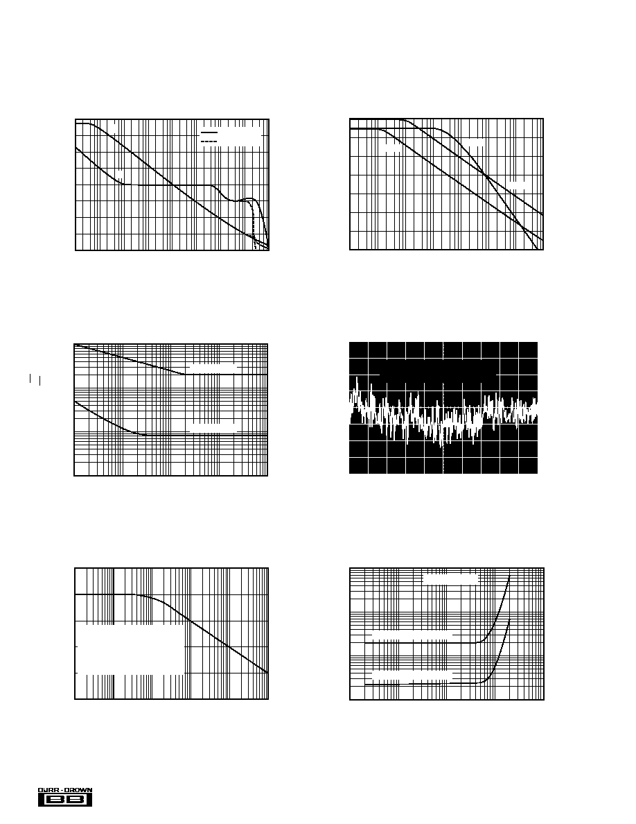
TYPICAL PERFORMANCE CURVES
At T
A
= +25
∞
C, V
S
=
±
15V, and R
L
= 2k
, unless otherwise noted.
50nV/div
1sec/div
INPUT NOISE VOLTAGE vs TIME
10
100
1k
10k
100k
Frequency (Hz)
CHANNEL SEPARATION vs FREQUENCY
1M
140
120
100
80
60
40
Channel Separation (dB)
Dual and quad devices. G = 1,
all channels. Quad measured
channel A to D or B to C--other
combinations yield similar or
improved rejection.
10
100
1k
10k
100k
1
0.1
0.01
0.001
THD+Noise (%)
Frequency (Hz)
TOTAL HARMONIC DISTORTION + NOISE
vs FREQUENCY
V
OUT
= 3.5Vrms
G = 10, R
L
= 2k
, 10k
G = 1, R
L
= 2k
, 10k
Noise signal is bandwidth limited to
lie between 0.1Hz and 10Hz.
1
10
100
1k
10k
1000
100
10
1
Voltage Noise (nV/
Hz)
Current Noise (fA/
Hz)
Frequency (Hz)
INPUT NOISE AND CURRENT NOISE
SPECTRAL DENSITY vs FREQUENCY
Current Noise
Voltage Noise
0.1
1
10
100
1k
10k
100k
1M
10M
140
120
100
80
60
40
20
0
≠20
A
OL
(dB)
0
≠30
≠60
≠90
≠120
≠150
≠180
Phase (∞)
Frequency (Hz)
OPEN-LOOP GAIN/PHASE
vs FREQUENCY
G
C
L
= 0
C
L
= 1500pF
0.1
1
10
100
1k
10k
100k
1M
140
120
100
80
60
40
20
0
PSR, CMR (dB)
Frequency (Hz)
POWER SUPPLY AND COMMON-MODE
REJECTION vs FREQUENCY
+PSR
CMR
≠PSR
5
OPA277, 2277, 4277
Æ
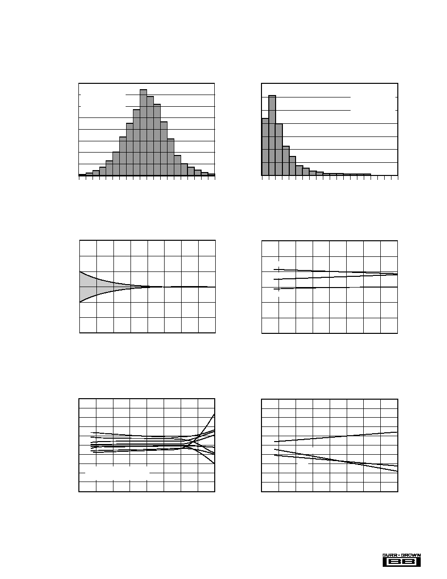
TYPICAL PERFORMANCE CURVES
(CONT)
At T
A
= +25
∞
C, V
S
=
±
15V, and R
L
= 2k
, unless otherwise noted.
OFFSET VOLTAGE PRODUCTION DISTRIBUTION
Percent of Amplifiers (%)
Offset Voltage (µV)
≠50≠45≠40≠35≠30≠25≠20≠15≠10 ≠5 0 5 10 15 20 25 30 35 40 45 50
16
14
12
10
8
6
4
2
0
Typical distribution
of packaged units.
Single, dual, and
quad included.
3
2
1
0
≠1
≠2
≠3
Offset Voltage Change (µV)
0
30
60
90
120
Time from Power Supply Turn-On (s)
WARM-UP OFFSET VOLTAGE DRIFT
15
45
75
105
OFFSET VOLTAGE DRIFT
PRODUCTION DISTRIBUTION
Percent of Amplifiers (%)
Offset Voltage (µV/∞C)
0
0.1
0.2
0.3
0.4
0.5
0.6
0.7
0.8
0.9
1.0
35
30
25
20
15
10
5
0
Typical distribution
of packaged units.
Single, dual, and
quad included.
INPUT BIAS CURRENT vs TEMPERATURE
125
Temperature (∞C)
≠75
≠50
≠25
0
25
50
75
100
5
4
3
2
1
0
≠1
≠2
≠3
≠4
≠5
Input Bias Current (nA)
Curves represent typical
production units.
≠75
≠50
≠25
0
25
50
75
100
125
160
150
140
130
120
110
100
A
OL
, CMR, PSR (dB)
Temperature (∞C)
A
OL
, CMR, PSR vs TEMPERATURE
CMR
A
OL
PSR
≠75
≠50
≠25
0
25
50
75
100
125
1000
950
900
850
800
750
700
650
600
550
500
Quiescent Current (µA)
100
90
80
70
60
50
40
30
20
10
0
Short-Circuit Current (mA)
Temperature (∞C)
QUIESCENT CURRENT AND
SHORT-CIRCUIT CURRENT vs TEMPERATURE
+I
SC
≠I
SC
±I
Q

6
Æ
OPA277, 2277, 4277
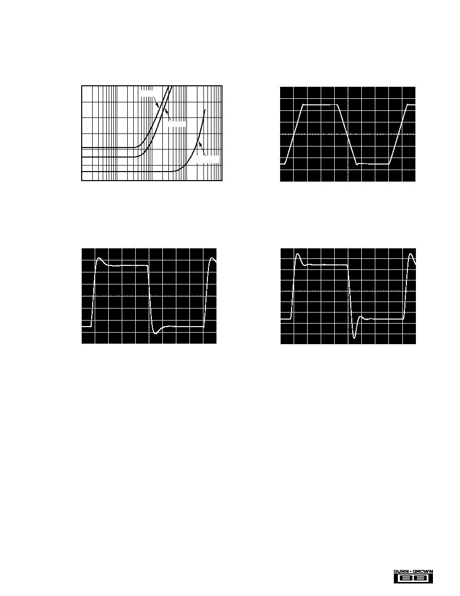
TYPICAL PERFORMANCE CURVES
(CONT)
At T
A
= +25
∞
C, V
S
=
±
15V, and R
L
= 2k
, unless otherwise noted.
CHANGE IN INPUT BIAS CURRENT
vs POWER SUPPLY VOLTAGE
40
Supply Voltage (V)
0
5
10
15
20
25
30
35
2.0
1.5
1.0
0.5
0.0
≠0.5
≠1.0
≠1.5
≠2.0
I
B
(nA)
Curve shows normalized change in
bias current with respect to V
S
= ±10V
(+20V). Typical I
B
may range from
≠0.5nA to +0.5nA at V
S
= ±10V.
V
CM
= 0V
CHANGE IN INPUT BIAS CURRENT
vs COMMON-MODE VOLTAGE
15
Common-Mode Voltage (V)
≠15
≠10
≠5
0
5
10
2.0
1.5
1.0
0.5
0.0
≠0.5
≠1.0
≠1.5
≠2.0
I
B
(nA)
V
S
= ±5V
V
S
= ±15V
Curve shows normalized change in bias current
with respect to V
CM
= 0V. Typical I
B
may range
from ≠05.nA to +0.5nA at V
CM
= 0V.
OUTPUT VOLTAGE SWING vs OUTPUT CURRENT
(V+)
(V+) ≠ 1
(V+) ≠ 2
(V+) ≠ 3
(V+) ≠ 4
(V+) ≠ 5
(V≠) + 5
(V≠) + 4
(V≠) + 3
(V≠) + 2
(V≠) + 1
(V≠)
0
±5
±10
±15
±20
±25
±30
Output Current (mA)
Output Voltage Swing (V)
≠55∞C
≠55∞C
125∞C
25∞C
125∞C
25∞C
1000
900
800
700
600
500
Quiescent Current (µA)
0
±5
±10
±15
±20
Supply Voltage (V)
QUIESCENT CURRENT vs SUPPLY VOLTAGE
per amplifier
MAXIMUM OUTPUT VOLTAGE
vs FREQUENCY
1M
Frequency (Hz)
1k
10k
100k
30
25
20
15
10
5
0
Output Voltage (Vp-p)
V
S
= ±15V
V
S
= ±5V
100
10
20
50
Settling Time (µs)
±1
±10
±100
Gain (V/V)
SETTLING TIME vs CLOSED-LOOP GAIN
0.01%
10V step
C
L
= 1500pF
0.1%
7
OPA277, 2277, 4277
Æ
TYPICAL PERFORMANCE CURVES
(CONT)
At T
A
= +25
∞
C, V
S
=
±
15V, and R
L
= 2k
, unless otherwise noted.
2V/div
20mV/div
20mV/div
10
µ
s/div
1
µ
s/div
1
µ
s/div
SMALL-SIGNAL STEP RESPONSE
G = +1, C
L
= 0, V
S
=
±
15V
SMALL-SIGNAL STEP RESPONSE
G = +1, C
L
= 1500pF, V
S
=
±
15V
LARGE-SIGNAL STEP RESPONSE
G = +1, C
L
= 1500pF, V
S
=
±
15V
SMALL-SIGNAL OVERSHOOT
vs LOAD CAPACITANCE
1k
100
10
10k
100k
Load Capacitance (pF)
60
50
40
30
20
10
0
Overshoot (%)
Gain = ≠1
Gain = +1
Gain = ±10
8
Æ
OPA277, 2277, 4277
Op Amp
(a)
OPA277
(b)
No bias current
cancellation resistor
(see text)
Conventional op amp with external bias
current cancellation resistor.
OPA277 with no external bias current
cancellation resistor.
R
2
R
1
R
2
R
1
R
B
= R
2
|| R
1
APPLICATIONS INFORMATION
The OPA277 series is unity-gain stable and free from unex-
pected output phase reversal, making it easy to use in a wide
range of applications. Applications with noisy or high im-
pedance power supplies may require decoupling capacitors
close to the device pins. In most cases 0.1
µ
F capacitors are
adequate.
The OPA277 series has very low offset voltage and drift. To
achieve highest performance, circuit layout and mechanical
conditions should be optimized. Offset voltage and drift can
be degraded by small thermoelectric potentials at the op amp
inputs. Connections of dissimilar metals will generate ther-
mal potential which can degrade the ultimate performance of
the OPA277 series. These thermal potentials can be made to
cancel by assuring that they are equal in both input termi-
nals.
∑ Keep thermal mass of the connections made to the two
input terminals similar.
∑ Locate heat sources as far as possible from the critical
input circuitry.
∑ Shield op amp and input circuitry from air currents such as
cooling fans.
OPERATING VOLTAGE
OPA277 series op amp operate from
±
2V to
±
18V supplies
with excellent performance. Unlike most op amps which are
specified at only one supply voltage, the OPA277 series is
specified for real-world applications; a single limit applies
over the
±
5V to
±
15V supply range. This allows a customer
operating at V
S
=
±
10V to have the same assured perfor-
mance as a customer using
±
15V supplies. In addition, key
parameters are guaranteed over the specified temperature
range, ≠40
∞
C to +85
∞
C. Most behavior remains unchanged
through the full operating voltage range (
±
2V to
±
18V).
Parameters which vary significantly with operating voltage
or temperature are shown in typical performance curves.
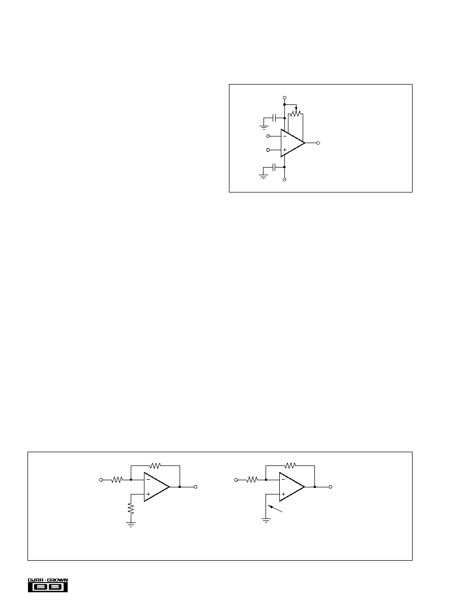
OFFSET VOLTAGE ADJUSTMENT
The OPA277 series is laser-trimmed for very low offset
voltage and drift so most circuits will not require external
adjustment. However, offset voltage trim connections are
provided on pins 1 and 8. Offset voltage can be adjusted by
connecting a potentiometer as shown in Figure 1. This
adjustment should be used only to null the offset of the op
amp. This adjustment should not be used to compensate for
offsets created elsewhere in a system since this can intro-
duce additional temperature drift.
INPUT PROTECTION
The inputs of the OPA277 series are protected with 1k
series input resistors and diode clamps. The inputs can
withstand
±
30V differential inputs without damage. The
protection diodes will, of course, conduct current when the
inputs are over-driven. This may disturb the slewing behav-
ior of unity-gain follower applications, but will not damage
the op amp.
INPUT BIAS CURRENT CANCELLATION
The input stage base current of the OPA277 series is inter-
nally compensated with an equal and opposite cancellation
circuit. The resulting input bias current is the difference
between the input stage base current and the cancellation
current. This residual input bias current can be positive or
negative.
When the bias current is canceled in this manner, the input
bias current and input offset current are approximately the
same magnitude. As a result, it is not necessary to use a bias
current cancellation resistor as is often done with other op
amps (Figure 2). A resistor added to cancel input bias
current errors may actually increase offset voltage and noise.
FIGURE 2. Input Bias Current Cancellation.
V+
V≠
20k
OPA277 single op amp only.
Use offset adjust pins only to null
offset voltage of op amp--see text.
Trim Range: Exceeds
Offset Voltage Specification
OPA277
6
7
8
4
3
2
1
0.1µF
0.1µF
FIGURE 1. OPA277 Offset Voltage Trim Circuit.
9
OPA277, 2277, 4277
Æ
R
1
V≠
1/2
OPA2277
R
2
1/2
OPA2277
V
OUT
= (V
1
≠ V
2
)(1 + )
R
2
R
1
V+
V+
V≠
R
2
For integrated solution see: INA126, INA2126 (dual)
INA125 (on-board reference)
INA122 (single-supply)
R
1
Load
Cell
R+
R
V
2
R≠
R
R≠
R
R+
R
V
1
14
1
12
5V
11
13
I
REG
1mA
4
3
2
6
R
G
1250
XTR105
1/2
OPA2277
7
R
G
R
G
V
IN
≠
V
IN
+
V
REG
I
R2
V+
I
RET
I
O
E
B
8
I
O
= 4mA + (V
IN
≠ V
IN
)
+
≠
40
R
G
9
10
R
F
10k
R
412
1/2
OPA2277
V+
V≠
Type J
25
(G = 1 + = 50)
2R
F
R
50
1k
R
F
10k
I
R1
V
LIN
R
CM
= 1250
0.01µF
FIGURE 3. Load Cell Amplifier.
FIGURE 4. Thermocouple Low Offset, Low Drift Loop Measurement with Diode Cold Junction Compensation.

PACKAGING INFORMATION
ORDERABLE DEVICE
STATUS(1)
PACKAGE TYPE
PACKAGE DRAWING
PINS
PACKAGE QTY
OPA2277P
ACTIVE
PDIP
P
8
50
OPA2277PA
ACTIVE
PDIP
P
8
50
OPA2277U
ACTIVE
SOIC
D
8
100
OPA2277U/2K5
ACTIVE
SOIC
D
8
2500
OPA2277UA
ACTIVE
SOIC
D
8
100
OPA2277UA/2K5
ACTIVE
SOIC
D
8
2500
OPA277P
ACTIVE
PDIP
P
8
50
OPA277PA
ACTIVE
PDIP
P
8
50
OPA277U
ACTIVE
SOIC
D
8
100
OPA277U/2K5
ACTIVE
SOIC
D
8
2500
OPA277UA
ACTIVE
SOIC
D
8
100
OPA277UA/2K5
ACTIVE
SOIC
D
8
2500
OPA4277PA
ACTIVE
PDIP
N
14
25
OPA4277UA
ACTIVE
SOIC
D
14
58
OPA4277UA/2K5
ACTIVE
SOIC
D
14
2500
(1) The marketing status values are defined as follows:
ACTIVE: Product device recommended for new designs.
LIFEBUY: TI has announced that the device will be discontinued, and a lifetime-buy period is in effect.
NRND: Not recommended for new designs. Device is in production to support existing customers, but TI does not recommend using this part in
a new design.
PREVIEW: Device has been announced but is not in production. Samples may or may not be available.
OBSOLETE: TI has discontinued the production of the device.
PACKAGE OPTION ADDENDUM
www.ti.com
12-Nov-2003

IMPORTANT NOTICE
Texas Instruments Incorporated and its subsidiaries (TI) reserve the right to make corrections, modifications,
enhancements, improvements, and other changes to its products and services at any time and to discontinue
any product or service without notice. Customers should obtain the latest relevant information before placing
orders and should verify that such information is current and complete. All products are sold subject to TI's terms
and conditions of sale supplied at the time of order acknowledgment.
TI warrants performance of its hardware products to the specifications applicable at the time of sale in
accordance with TI's standard warranty. Testing and other quality control techniques are used to the extent TI
deems necessary to support this warranty. Except where mandated by government requirements, testing of all
parameters of each product is not necessarily performed.
TI assumes no liability for applications assistance or customer product design. Customers are responsible for
their products and applications using TI components. To minimize the risks associated with customer products
and applications, customers should provide adequate design and operating safeguards.
TI does not warrant or represent that any license, either express or implied, is granted under any TI patent right,
copyright, mask work right, or other TI intellectual property right relating to any combination, machine, or process
in which TI products or services are used. Information published by TI regarding third-party products or services
does not constitute a license from TI to use such products or services or a warranty or endorsement thereof.
Use of such information may require a license from a third party under the patents or other intellectual property
of the third party, or a license from TI under the patents or other intellectual property of TI.
Reproduction of information in TI data books or data sheets is permissible only if reproduction is without
alteration and is accompanied by all associated warranties, conditions, limitations, and notices. Reproduction
of this information with alteration is an unfair and deceptive business practice. TI is not responsible or liable for
such altered documentation.
Resale of TI products or services with statements different from or beyond the parameters stated by TI for that
product or service voids all express and any implied warranties for the associated TI product or service and
is an unfair and deceptive business practice. TI is not responsible or liable for any such statements.
Following are URLs where you can obtain information on other Texas Instruments products and application
solutions:
Products
Applications
Amplifiers
amplifier.ti.com
Audio
www.ti.com/audio
Data Converters
dataconverter.ti.com
Automotive
www.ti.com/automotive
DSP
dsp.ti.com
Broadband
www.ti.com/broadband
Interface
interface.ti.com
Digital Control
www.ti.com/digitalcontrol
Logic
logic.ti.com
Military
www.ti.com/military
Power Mgmt
power.ti.com
Optical Networking
www.ti.com/opticalnetwork
Microcontrollers
microcontroller.ti.com
Security
www.ti.com/security
Telephony
www.ti.com/telephony
Video & Imaging
www.ti.com/video
Wireless
www.ti.com/wireless
Mailing Address:
Texas Instruments
Post Office Box 655303 Dallas, Texas 75265
Copyright
2003, Texas Instruments Incorporated