
1
Æ
OPA340/2340/4340
1
2
3
4
5
6
7
8
16
15
14
13
12
11
10
9
Out D
≠In D
+In D
≠V
+In C
≠In C
Out C
NC
Out A
≠In A
+In A
+V
+In B
≠In B
Out B
NC
OPA4340
SSOP-16
A
D
B
C
1
2
3
4
8
7
6
5
V+
Out B
≠In B
+In B
Out A
≠In A
+In A
V≠
OPA2340
8-Pin DIP, SO-8, MSOP-8
A
B
1
2
3
4
8
7
6
5
NC
V+
Output
NC
NC
≠In
+In
V≠
OPA340
8-Pin DIP, SO-8
1
2
3
5
4
V+
≠In
Out
V≠
+In
OPA340
SOT-23-5
SINGLE-SUPPLY, RAIL-TO-RAIL
OPERATIONAL AMPLIFIERS
Micro
Amplifier
TM
Series
FEATURES
q
RAIL-TO-RAIL INPUT
q
RAIL-TO-RAIL OUTPUT (within 1mV)
q
Micro
SIZE PACKAGES
q
WIDE BANDWIDTH: 5.5MHz
q
HIGH SLEW RATE: 6V/
µ
s
q
LOW THD+NOISE: 0.0007% (f = 1kHz)
q
LOW QUIESCENT CURRENT: 750
µ
A/channel
q
SINGLE, DUAL, AND QUAD
International Airport Industrial Park ∑ Mailing Address: PO Box 11400, Tucson, AZ 85734 ∑ Street Address: 6730 S. Tucson Blvd., Tucson, AZ 85706 ∑ Tel: (520) 746-1111 ∑ Twx: 910-952-1111
Internet: http://www.burr-brown.com/ ∑ FAXLine: (800) 548-6133 (US/Canada Only) ∑ Cable: BBRCORP ∑ Telex: 066-6491 ∑ FAX: (520) 889-1510 ∑ Immediate Product Info: (800) 548-6132
APPLICATIONS
q
DRIVING A/D CONVERTERS
q
PCMCIA CARDS
q
DATA ACQUISITION
q
PROCESS CONTROL
q
AUDIO PROCESSING
q
COMMUNICATIONS
q
ACTIVE FILTERS
q
TEST EQUIPMENT
DESCRIPTION
OPA340 series rail-to-rail CMOS operational amplifi-
ers are optimized for low voltage, single supply opera-
tion. Rail-to-rail input/output and high speed operation
make them ideal for driving sampling analog-to-digital
converters. They are also well suited for general pur-
pose and audio applications as well as providing I/V
conversion at the output of D/A converters. Single,
dual, and quad versions have identical specifications
for design flexibility.
The OPA340 series operates on a single supply as low as
2.5V with an input common-mode voltage range that
extends 500mV below ground and 500mV above the
positive supply. Output voltage swing is to within 1mV
of the supply rails with a 100k
load. They offer excel-
lent dynamic response (BW = 5.5MHz, SR = 6V/
µ
s), yet
quiescent current is only 750
µ
A. Dual and quad designs
feature completely independent circuitry for lowest
crosstalk and freedom from interaction.
The single (OPA340) packages are the tiny 5-lead
SOT-23-5 surface mount, SO-8 surface mount, and
8-pin DIP. The dual (OPA2340) comes in the minia-
ture MSOP-8 surface mount, SO-8 surface mount,
and 8-pin DIP packages. The quad (OPA4340) pack-
ages are the space-saving SSOP-16 surface mount,
SO-14 surface mount, and the 14-pin DIP. All are
specified from ≠40
∞
C to +85
∞
C and operate from
≠55
∞
C to +125
∞
C. A SPICE macromodel is available
for design analysis.
OPA4340
OPA340
OPA2340
OPA4340
Æ
OPA340
OPA2340
OPA4340
© 1997 Burr-Brown Corporation
PDS-1404C
Printed in U.S.A. December, 1997
SBOS073

2
Æ
OPA340/2340/4340
SPECIFICATIONS: V
S
= 2.7V to 5V
At T
A
= +25
∞
C, R
L
= 10k
connected to V
S
/2 and V
OUT
= V
S
/2, unless otherwise noted.
Boldface limits apply over the specified temperature range, T
A
= ≠40
∞
C to +85
∞
C. V
S
= 5V.
PARAMETER
CONDITION
MIN
TYP
(1)
MAX
UNITS
OFFSET VOLTAGE
Input Offset Voltage
V
OS
V
S
= 5V
±
150
±
500
µ
V
vs Temperature
dV
OS
/dT
±
2.5
µ
V/
∞
C
vs Power Supply
PSRR
V
S
= 2.7V to 5.5V, V
CM
= 0V
30
120
µ
V/V
T
A
= ≠40
∞
C to +85
∞
C
V
S
= 2.7V to 5.5V, V
CM
= 0V
120
µ
V/V
Channel Separation, dc
0.2
µ
V/V
INPUT BIAS CURRENT
Input Bias Current
I
B
±
0.2
±
10
pA
T
A
= ≠40
∞
C to +85
∞
C
±
60
pA
Input Offset Current
I
OS
±
0.2
±
10
pA
NOISE
Input Voltage Noise, f = 0.1 to 50kHz
8
µ
Vrms
Input Voltage Noise Density, f = 1kHz
e
n
25
nV/
Hz
Current Noise Density, f = 1kHz
i
n
3
fA/
Hz
INPUT VOLTAGE RANGE
Common-Mode Voltage Range
V
CM
≠0.3
(V+) +0.3
V
Common-Mode Rejection Ratio
CMRR
≠0.3V < V
CM
< (V+) ≠1.8V
80
92
dB
V
S
= 5V, ≠0.3V
< V
CM
< 5.3V
70
84
dB
V
S
= 2.7V, ≠0.3V
< V
CM
< 3V
66
80
dB
INPUT IMPEDANCE
Differential
10
13
|| 3
|| pF
Common-Mode
10
13
|| 6
|| pF
OPEN-LOOP GAIN
Open-Loop Voltage Gain
A
OL
R
L
= 100k
, 5mV < V
O
< (V+) ≠5mV
106
124
dB
T
A
= ≠40
∞
C to +85
∞
C
R
L
= 100k
, 5mV < V
O
< (V+) ≠5mV
106
dB
R
L
= 10k
, 50mV < V
O
< (V+) ≠50mV
100
120
dB
T
A
= ≠40
∞
C to +85
∞
C
R
L
= 10k
, 50mV < V
O
< (V+) ≠50mV
100
dB
R
L
= 2k
, 200mV < V
O
< (V+) ≠200mV
94
114
dB
T
A
= ≠40
∞
C to +85
∞
C
R
L
= 2k
, 200mV < V
O
< (V+) ≠200mV
94
dB
FREQUENCY RESPONSE
Gain-Bandwidth Product
GBW
G = 1
5.5
MHz
Slew Rate
SR
V
S
= 5V, G = 1, C
L
= 100pF
6
V/
µ
s
Settling Time, 0.1%
V
S
= 5V, 2V Step, C
L
= 100pF
1
µ
s
0.01%
V
S
= 5V, 2V Step, C
L
= 100pF
1.6
µ
s
Overload Recovery Time
V
IN
∑ G = V
S
0.2
µ
s
Total Harmonic Distortion + Noise
THD+N
V
S
= 5V, V
O
= 3Vp-p
(2)
, G = 1, f = 1kHz
0.0007
%
OUTPUT
Voltage Output Swing from Rail
(3)
R
L
= 100k
, A
OL
106dB
1
5
mV
T
A
= ≠40
∞
C to +85
∞
C
R
L
= 100k
,
A
OL
106dB
5
mV
R
L
= 10k
,
A
OL
100dB
10
50
mV
T
A
= ≠40
∞
C to +85
∞
C
R
L
= 10k
, A
OL
100dB
50
mV
R
L
= 2k
,
A
OL
94dB
40
200
mV
T
A
= ≠40
∞
C to +85
∞
C
R
L
= 2k
, A
OL
94dB
200
mV
Short-Circuit Current
I
SC
±
50
mA
Capacitive Load Drive
C
LOAD
See Typical Curve
POWER SUPPLY
Specified Voltage Range
V
S
2.7
5
V
Operating Voltage Range
2.5 to 5.5
V
Quiescent Current (per amplifier)
I
Q
I
O
= 0, V
S
= +5V
750
950
µ
A
T
A
= ≠40
∞
C to +85
∞
C
I
O
= 0, V
S
= +5V
1100
µ
A
TEMPERATURE RANGE
Specified Range
≠40
+85
∞
C
Operating Range
≠55
+125
∞
C
Storage Range
≠55
+125
∞
C
Thermal Resistance
JA
SOT-23-5 Surface Mount
200
∞
C/W
MSOP-8 Surface Mount
150
∞
C/W
SO-8 Surface Mount
150
∞
C/W
8-Pin DIP
100
∞
C/W
SSOP-16 Surface Mount
100
∞
C/W
SO-14 Surface Mount
100
∞
C/W
14-Pin DIP
80
∞
C/W
NOTES: (1) V
S
= +5V. (2) V
OUT
= 0.25V to 3.25V. (3) Output voltage swings are measured between the output and power supply rails.
OPA340NA, PA, UA
OPA2340EA, PA, UA
OPA4340EA, PA, UA

3
Æ
OPA340/2340/4340
1
2
3
4
5
6
7
14
13
12
11
10
9
8
Out D
≠In D
+In D
V≠
+In C
≠In C
Out C
Out A
≠In A
+In A
V+
+In B
≠In B
Out B
OPA4340
A
D
B
C
PACKAGE/ORDERING INFORMATION
Supply Voltage ................................................................................... 5.5V
Signal Input Terminals, Voltage
(2)
.................... (V≠) ≠0.5V to (V+) +0.5V
Current
(2)
.................................................... 10mA
Output Short-Circuit
(3)
.............................................................. Continuous
Operating Temperature ................................................. ≠55
∞
C to +125
∞
C
Storage Temperature ..................................................... ≠55
∞
C to +125
∞
C
Junction Temperature ...................................................................... 150
∞
C
Lead Temperature (soldering, 10s) ................................................. 300
∞
C
NOTES: (1) Stresses above these ratings may cause permanent damage.
(2) Input terminals are diode-clamped to the power supply rails. Input signals
that can swing more than 0.5V beyond the supply rails should be current-
limited to 10mA or less. (3) Short-circuit to ground, one amplifier per
package.
ABSOLUTE MAXIMUM RATINGS
(1)
PIN CONFIGURATIONS
Top View
SOIC/DIP
PACKAGE
SPECIFIED
DRAWING
TEMPERATURE
PACKAGE
ORDERING
TRANSPORT
PRODUCT
PACKAGE
NUMBER
(1)
RANGE
MARKING
NUMBER
(2)
MEDIA
Single
OPA340NA
5-Lead SOT-23-5
331
≠40
∞
C to +85
∞
C
A40
OPA340NA-250
Tape and Reel
"
"
"
"
"
OPA340NA-3K
Tape and Reel
OPA340PA
8-Pin DIP
006
≠40
∞
C to +85
∞
C
OPA340PA
OPA340PA
Rails
OPA340UA
SO-8 Surface-Mount
182
≠40
∞
C to +85
∞
C
OPA340UA
OPA340UA
Rails
(3)
Dual
OPA2340EA
MSOP-8 Surface-Mount
337
≠40
∞
C to +85
∞
C
A40A
OPA2340EA-250
Tape and Reel
"
"
"
"
"
OPA2340EA-2500
Tape and Reel
OPA2340PA
8-Pin DIP
006
≠40
∞
C to +85
∞
C
OPA2340PA
OPA2340PA
Rails
OPA2340UA
SO-8 Surface-Mount
182
≠40
∞
C to +85
∞
C
OPA2340UA
OPA2340UA
Rails
(3)
Quad
OPA4340EA
SSOP-16 Surface-Mount
322
≠40
∞
C to +85
∞
C
OPA4340EA
OPA4340EA-250
Tape and Reel
"
"
"
"
"
OPA4340EA-2500
Tape and Reel
OPA4340PA
14-Pin DIP
010
≠40
∞
C to +85
∞
C
OPA4340PA
OPA4340PA
Rails
OPA4340UA
SO-14 Surface Mount
235
≠40
∞
C to +85
∞
C
OPA4340UA
OPA4340UA
Rails
(3)
NOTES: (1) For detailed drawing and dimension table, please see end of data sheet, or Appendix C of Burr-Brown IC Data Book. (2) Models with -250, -2500, and
-3K are available only in Tape and Reel in the quantities indicated (e.g., -250 indicates 250 devices per reel). Ordering 3000 pieces of "OPA340NA-3K" will get
a single 3000 piece Tape and Reel. For detailed Tape and Reel mechanical information, refer to Appendix B of Burr-Brown IC Data Book. (3) SO-8 and SO-14
models also available in Tape and Reel.
The information provided herein is believed to be reliable; however, BURR-BROWN assumes no responsibility for inaccuracies or omissions. BURR-BROWN assumes no responsibility
for the use of this information, and all use of such information shall be entirely at the user's own risk. Prices and specifications are subject to change without notice. No patent rights or
licenses to any of the circuits described herein are implied or granted to any third party. BURR-BROWN does not authorize or warrant any BURR-BROWN product for use in life support
devices and/or systems.
ELECTROSTATIC
DISCHARGE SENSITIVITY
This integrated circuit can be damaged by ESD. Burr-Brown
recommends that all integrated circuits be handled with
appropriate precautions. Failure to observe proper handling
and installation procedures can cause damage.
ESD damage can range from subtle performance degrada-
tion to complete device failure. Precision integrated circuits
may be more susceptible to damage because very small
parametric changes could cause the device not to meet its
published specifications.
4
Æ
OPA340/2340/4340
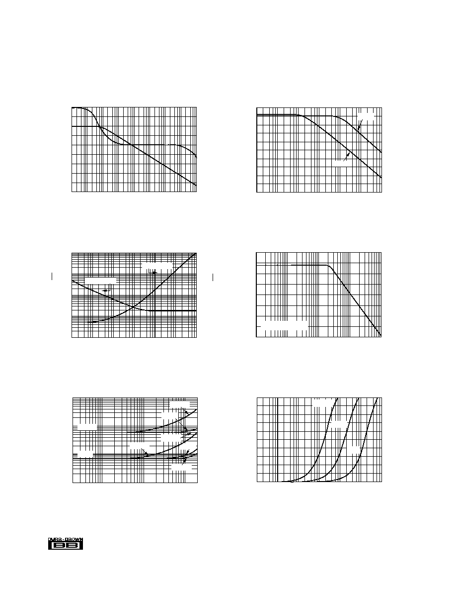
TYPICAL PERFORMANCE CURVES
At T
A
= +25
∞
C, V
S
= +5V, and R
L
= 10k
connected to V
S
/2, unless otherwise noted.
CLOSED-LOOP OUTPUT IMPEDANCE
vs FREQUENCY
5k
4k
3k
2k
1k
0
Output Resistance (
)
Frequency (Hz)
10
100
1k
10k
100k
1M
10M
G = 100
G = 10
G = 1
CHANNEL SEPARATION vs FREQUENCY
Frequency (Hz)
Channel Separation (dB)
140
130
120
110
100
100
10
1k
10k
100k
G = 1, All Channels
OPEN-LOOP GAIN/PHASE vs FREQUENCY
0.1
1
160
140
120
100
80
60
40
20
0
≠20
Voltage Gain (dB)
0
≠45
≠90
≠135
≠180
Phase (∞)
Frequency (Hz)
10
100
1k
10k
100k
1M
10M
INPUT VOLTAGE AND CURRENT NOISE
SPECTRAL DENSITY vs FREQUENCY
10k
1k
100
10
1
1k
100
10
1
0.1
Voltage Noise (nV
Hz)
Frequency (Hz)
1
10
100
1k
10k
100k
1M
Current Noise (fA
Hz)
Current Noise
Voltage Noise
TOTAL HARMONIC DISTORTION + NOISE
vs FREQUENCY
0.1
0.01
0.001
0.0001
THD+N (%)
Frequency (Hz)
20
100
1k
10k
20k
R
L
= 600
G = 10
G = 1
R
L
= 2k
R
L
= 2k
R
L
= 10k
R
L
= 600
R
L
= 10k
POWER SUPPLY and COMMON-MODE
REJECTION vs FREQUENCY
100
80
60
40
20
0
PSRR, CMRR (dB)
Frequency (Hz)
1
10
100
1k
10k
100k
1M
PSRR
CMRR
5
Æ
OPA340/2340/4340
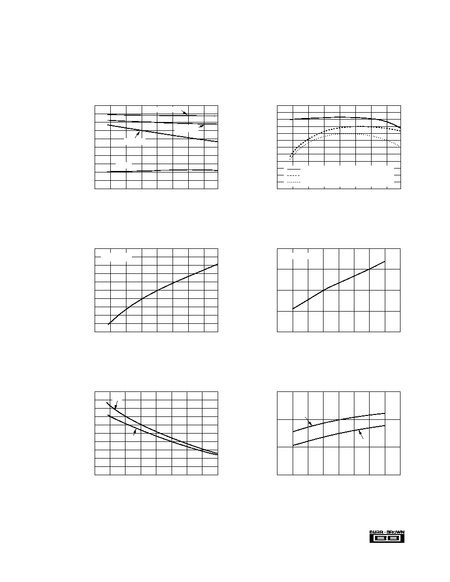
TYPICAL PERFORMANCE CURVES
(CONT)
At T
A
= +25
∞
C, V
S
= +5V, and R
L
= 10k
connected to V
S
/2, unless otherwise noted.
QUIESCENT CURRENT vs TEMPERATURE
1000
900
800
700
600
500
Quiescent Current (µA)
Temperature (∞C)
≠75
≠50
≠25
0
25
50
75
100
125
Per Amplifier
SHORT-CIRCUIT CURRENT vs TEMPERATURE
Temperature (∞C)
Short-Circuit Current (mA)
100
90
80
70
60
50
40
30
20
10
0
≠75
≠50
≠25
0
25
50
75
100
125
≠I
SC
+I
SC
SHORT-CIRCUIT CURRENT vs SUPPLY VOLTAGE
Supply Voltage (V)
Short-Circuit Current (mA)
60
50
40
30
2.0
2.5
3.0
3.5
4.0
4.5
5.0
5.5
6.0
+I
SC
≠I
SC
COMMON-MODE REJECTION vs TEMPERATURE
100
90
80
70
60
50
40
CMRR (dB)
Temperature (∞C)
≠75
≠50
≠25
0
25
50
75
100
125
V
S
= 5V, V
CM
= ≠0.3V to 5.3V
V
S
= 2.7V, V
CM
= ≠0.3V to 3V
V
S
= 2.7V to 5V, V
CM
= ≠0.3V to (V+) ≠1.8V
QUIESCENT CURRENT vs SUPPLY VOLTAGE
Supply Voltage (V)
Quiescent Current (
µ
A)
800
750
700
650
600
2.0
2.5
3.0
3.5
4.0
4.5
5.0
5.5
6.0
Per Amplifier
OPEN-LOOP GAIN AND POWER SUPPLY REJECTION
vs TEMPERATURE
130
120
110
100
90
80
A
OL
, PSRR (dB)
Temperature (∞C)
≠75
≠50
≠25
0
25
50
75
100
125
R
L
= 100k
R
L
= 10k
R
L
= 2k
A
OL
PSRR