1
Æ
OPA541
OPA541
DESCRIPTION
The OPA541 is a power operational amplifier capable
of operation from power supplies up to
±
40V and
delivering continuous output currents up to 5A. Inter-
nal current limit circuitry can be user-programmed
with a single external resistor, protecting the amplifier
and load from fault conditions. The OPA541 is fabri-
cated using a proprietary bipolar/FET process.
Pinout is compatible with popular hybrid power am-
plifiers such as the OPA511, OPA512 and the 3573.
High Power Monolithic
OPERATIONAL AMPLIFIER
APPLICATIONS
q
MOTOR DRIVER
q
SERVO AMPLIFIER
q
SYNCHRO EXCITATION
q
AUDIO AMPLIFIER
q
PROGRAMMABLE POWER SUPPLY
FEATURES
q
POWER SUPPLIES TO
±
40V
q
OUTPUT CURRENT TO 10A PEAK
q
PROGRAMMABLE CURRENT LIMIT
q
INDUSTRY-STANDARD PIN OUT
q
FET INPUT
q
TO-3 AND LOW-COST POWER PLASTIC
PACKAGES
The OPA541 uses a single current-limit resistor to set
both the positive and negative current limits. Applica-
tions currently using hybrid power amplifiers requir-
ing two current-limit resistors need not be modified.
The OPA541 is available in an 11-pin power plastic
package and an industry-standard 8-pin TO-3 her-
metic package. The power plastic package has a cop-
per-lead frame to maximize heat transfer. The TO-3
package is isolated from all circuitry, allowing it to be
mounted directly to a heat sink without special insula-
tors.
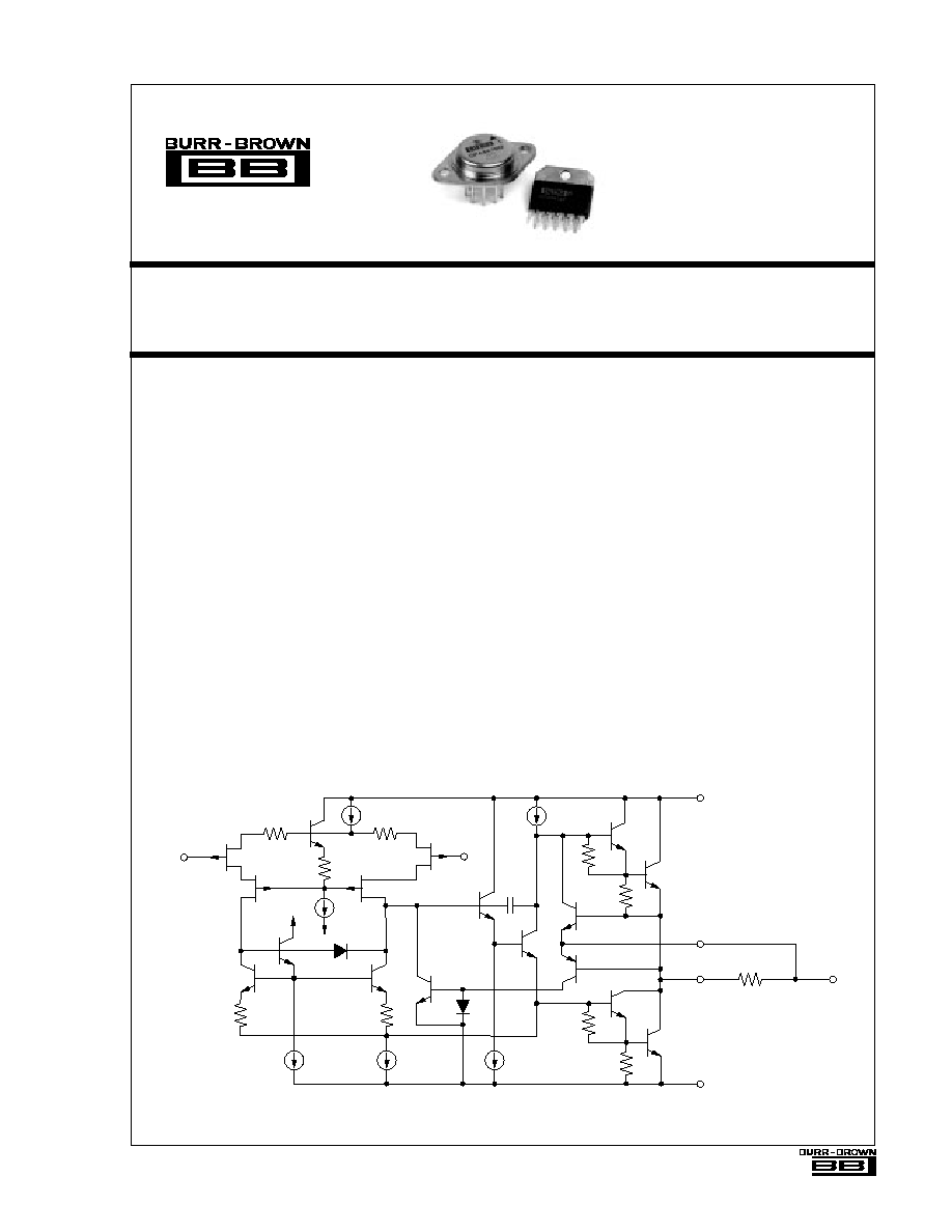
Current
Sense
Output
Drive
R
CL
+In
≠In
External
+V
S
≠V
S
V
O
PDS-737H
Æ
International Airport Industrial Park ∑ Mailing Address: PO Box 11400, Tucson, AZ 85734 ∑ Street Address: 6730 S. Tucson Blvd., Tucson, AZ 85706 ∑ Tel: (520) 746-1111 ∑ Twx: 910-952-1111
Internet: http://www.burr-brown.com/ ∑ FAXLine: (800) 548-6133 (US/Canada Only) ∑ Cable: BBRCORP ∑ Telex: 066-6491 ∑ FAX: (520) 889-1510 ∑ Immediate Product Info: (800) 548-6132
SBOS153

2
Æ
OPA541
SPECIFICATIONS
ELECTRICAL
At T
C
= +25
∞
C and V
S
=
±
35VDC, unless otherwise noted.
OPA541AM/AP
OPA541BM/SM
PARAMETER
CONDITIONS
MIN
TYP
MAX
MIN
TYP
MAX
UNITS
INPUT OFFSET VOLTAGE
V
OS
±
2
±
10
±
0.1
±
1
mV
vs Temperature
Specified Temperature Range
±
20
±
40
±
15
±
30
µ
V/
∞
C
vs Supply Voltage
V
S
=
±
10V to
±
V
MAX
±
2.5
±
10
T
T
µ
V/V
vs Power
±
20
±
60
T
T
µ
V/W
INPUT BIAS CURRENT
I
B
4
50
T
T
pA
INPUT OFFSET CURRENT
I
OS
±
1
±
30
T
T
pA
Specified Temperature Range
5
T
nA
INPUT CHARACTERISTICS
Common-Mode Voltage Range
Specified Temperature Range
±
(|V
S
| ≠ 6)
±
(|V
S
| ≠ 3)
T
T
V
Common-Mode Rejection
V
CM
= (|
±
V
S
| ≠ 6V)
95
113
T
T
dB
Input Capacitance
5
T
pF
Input Impedance, DC
1
T
T
GAIN CHARACTERISTICS
Open Loop Gain at 10Hz
R
L
= 6
90
97
T
T
dB
Gain-Bandwidth Product
1.6
T
MHz
OUTPUT
Voltage Swing
I
O
= 5A, Continuous
±
(|V
S
| ≠ 5.5)
±
(|V
S
| ≠ 4.5)
T
T
V
I
O
= 2A
±
(|V
S
| ≠ 4.5)
±
(|V
S
| ≠ 3.6)
T
T
V
I
O
= 0.5A
±
(|V
S
| ≠ 4)
±
(|V
S
| ≠ 3.2)
T
T
V
Current, Peak
9
10
T
T
A
AC PERFORMANCE
Slew Rate
6
10
T
T
V/
µ
s
Power Bandwidth
R
L
= 8
, V
O
= 20Vrms
45
55
T
T
kHz
Settling Time to 0.1%
2V Step
2
T
µ
s
Capacitive Load
Specified Temperature Range, G = 1
3.3
T
nF
Specified Temperature Range, G >10
SOA
(1)
T
Phase Margin
Specified Temperature Range, R
L
= 8
40
T
Degrees
POWER SUPPLY
Power Supply Voltage,
±
V
S
Specified Temperature Range
±
10
±
30
±
35
T
±
35
±
40
V
Current, Quiescent
20
25
T
T
mA
THERMAL RESISTANCE
JC
(Junction-to-Case)
(2)
AC Output f > 60Hz
2.5
∞
C/W
JC
(2)
DC Output
3
∞
C/W
JA
(Junction-to-Ambient)
No Heat Sink
40
∞
C/W
OPA541AP (Plastic)
40
∞
C/W
TEMPERATURE RANGE
T
CASE
AM, BM, AP
≠25
+85
T
T
∞
C
SM
≠55
+125
∞
C
T
Specification same as OPA541AM/AP.
NOTE: (1) SOA is the Safe Operating Area shown in Figure 1. (2) Plastic package may require insulator which typically adds 1
∞
C/W.
The information provided herein is believed to be reliable; however, BURR-BROWN assumes no responsibility for inaccuracies or omissions. BURR-BROWN assumes
no responsibility for the use of this information, and all use of such information shall be entirely at the user's own risk. Prices and specifications are subject to change
without notice. No patent rights or licenses to any of the circuits described herein are implied or granted to any third party. BURR-BROWN does not authorize or warrant
any BURR-BROWN product for use in life support devices and/or systems.
3
Æ
OPA541
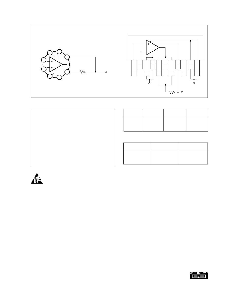
Top View
TO≠3
Plastic Package
CONNECTION DIAGRAMS
≠In
NC
+In
NC
V
O
Output
Drive
R
CL
≠V
S
+V
S
Current
Sense
1
3
5
7
9
11
2
4
6
8
10
Tab at ≠V
S
Current
Sense
≠V
S
+In
≠In
+V
S
NC
NC
Output
Drive
R
CL
V
O
1
2
3
8
5
6
4
7
ORDERING INFORMATION
TEMPERATURE
CONTINUOUS
PRODUCT
PACKAGE
RANGE
CURRENT
OPA541AP
Power Plastic
≠25
∞
C to +85
∞
C
5A at 25
∞
C
OPA541AM
TO-3
≠25
∞
C to +85
∞
C
5A at 25
∞
C
OPA541BM
TO-3
≠25
∞
C to +85
∞
C
5A at 25
∞
C
OPA541SM
TO-3
≠55
∞
C to +125
∞
C
5A at 25
∞
C
ABSOLUTE MAXIMUM RATINGS
Supply Voltage, +V
S
to ≠V
S
............................................................... 80V
Output Current ............................................................................. see SOA
Power Dissipation, Internal
(1)
........................................................... 125W
Input Voltage: Differential ....................................................................
±
V
S
Common-mode .............................................................
±
V
S
Temperature: Pin solder, 10s ........................................................ +300
∞
C
Junction
(1)
............................................................... +150
∞
C
Temperature Range:
AM, BM SM
Storage .................................................................... ≠65
∞
C to +150
∞
C
Operating (case) ...................................................... ≠55
∞
C to +125
∞
C
AP
Storage ...................................................................... ≠40
∞
C to +85
∞
C
Operating (case) ........................................................ ≠25
∞
C to +85
∞
C
NOTE: (1) Long term operation at the maximum junction temperature will
result in reduced product life. Derate internal power dissipation to achieve
high MTTF.
PACKAGE INFORMATION
PACKAGE DRAWING
PRODUCT
PACKAGE
NUMBER
(1)
OPA541AP
Power Plastic
242
OPA541AM
TO-3
030
OPA541BM
TO-3
030
OPA541SM
TO-3
030
NOTE: (1) For detailed drawing and dimension table, please see end of data
sheet, or Appendix C of Burr-Brown IC Data Book.
ELECTROSTATIC
DISCHARGE SENSITIVITY
This integrated circuit can be damaged by ESD. Burr-Brown
recommends that all integrated circuits be handled with
appropriate precautions. Failure to observe proper handling
and installation procedures can cause damage.
ESD damage can range from subtle performance degradation
to complete device failure. Precision integrated circuits may
be more susceptible to damage because very small parametric
changes could cause the device not to meet its published
specifications.
4
Æ
OPA541
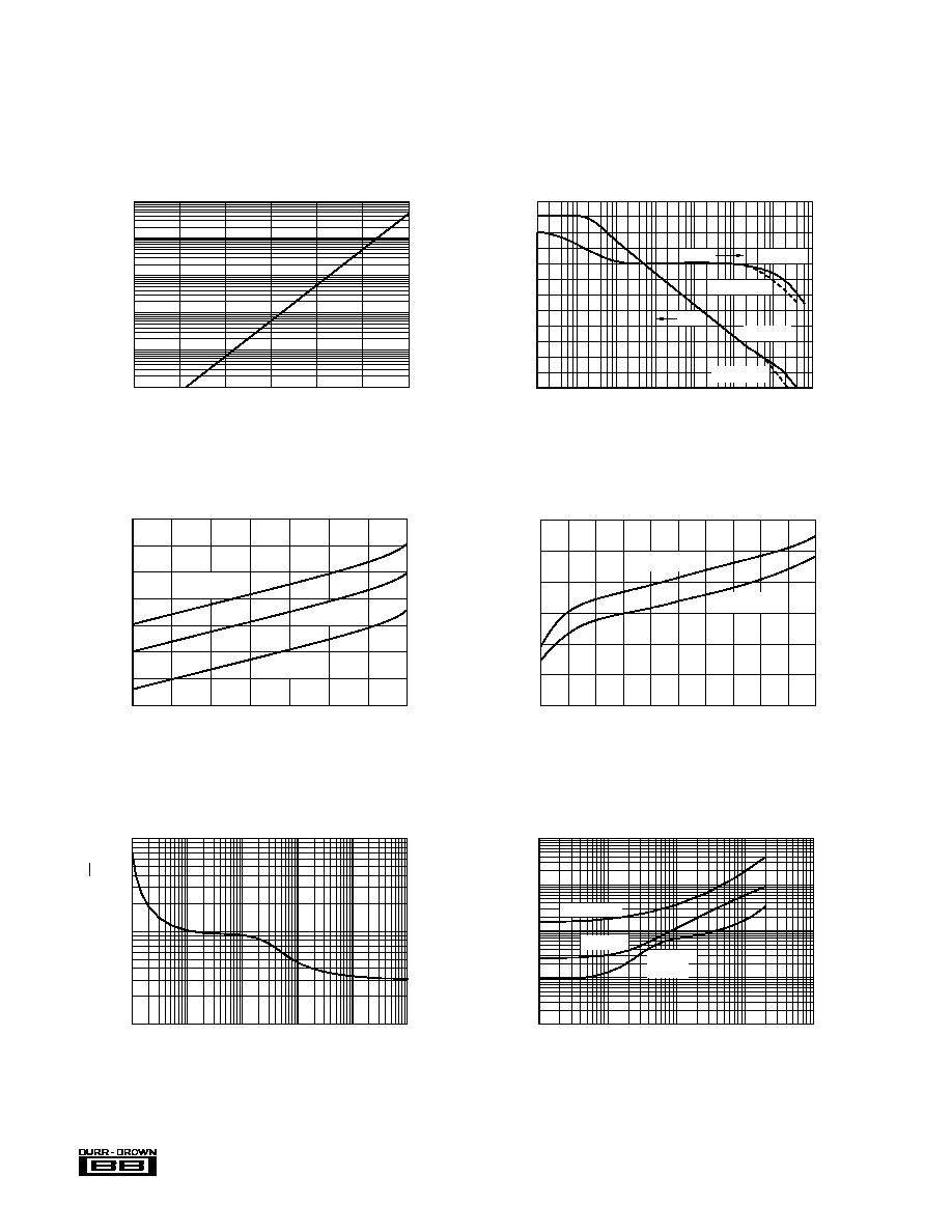
10
1
0.1
0.01
0.001
10
100
1k
10k
100k
Frequency (Hz)
THD + Noise (%)
TOTAL HARMONIC DISTORTION + NOISE
vs FREQUENCY
P = 100mW
O
P = 50W
O
A = ≠5
V
P = 5W
O
1k
100
10
Voltage Noise Density (nV/
Hz)
VOLTAGE NOISE DENSITY
vs FREQUENCY
1
10
100
1k
10k
100k
Frequency (Hz)
6
5
4
3
2
1
0
0
1
2
3
4
5
6
7
8
9
10
I (A)
OUT
|±V | ≠ |V | (V)
OUT
S
OUTPUT VOLTAGE SWING
vs OUTPUT CURRENT
|≠V | ≠ |V |
S
O
(+V ) ≠ V
S
O
1.3
1.2
1.1
1
0.9
0.8
0.7
0.6
20
30
40
50
60
70
80
90
+V + |≠V | (V)
S
S
Normalized I
NORMALIZED QUIESCENT CURRENT
vs TOTAL POWER SUPPLY VOLTAGE
T = +25∞C
C
T = ≠25∞C
C
T = +125∞C
C
Q
110
90
70
50
30
10
≠10
1
10
100
1k
10k
100k
1M
10M
Frequency (Hz)
Voltage Gain (dB)
OPEN-LOOP GAIN AND PHASE
vs FREQUENCY
0
≠45
≠90
≠135
≠180
Phase (Degrees)
Phase
Gain
Z = 3.3nF
L
Z = 3.3nF
L
Z = 2k
L
Z = 2k
L
≠25
0
25
50
75
100
125
100
10
1
0.1
0.01
0.001
Input Bias Current (nA)
Temperature (∞C)
INPUT BIAS CURRENT
vs TEMPERATURE
TYPICAL PERFORMANCE CURVES
At T
A
= +25
∞
C, V
S
=
±
35VDC, unless otherwise noted.
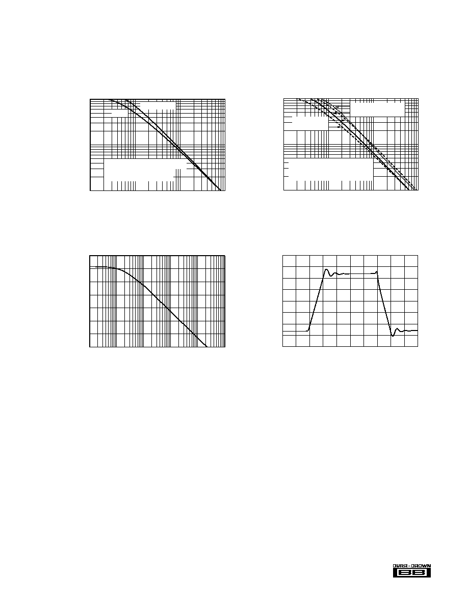
5
Æ
OPA541
120
110
100
90
80
70
60
50
10
100
1k
10k
100k
1M
Frequency (Hz)
CMRR (dB)
COMMON-MODE REJECTION
vs FREQUENCY
10
1
0.1
0.01
0.1
1
10
R ( )
CL
I (A)
LIMIT
CURRENT LIMIT
vs RESISTANCE LIMIT
TO-3
Power Plastic
NOTE: These are averaged values.
≠I is typically 10% higher.
+I is typically 10% lower.
OUT
OUT
TYPICAL PERFORMANCE CURVES
(CONT)
At T
A
= +25
∞
C, V
S
=
±
35VDC, unless otherwise noted.
Time (1µs/division)
DYNAMIC RESPONSE
Voltage (2V/division)
10
1
0.1
0.01
0.1
1
10
R ( )
CL
I (A)
LIMIT
CURRENT LIMIT vs RESISTANCE LIMIT
vs TEMPERATURE
Power Plastic at ≠25∞C
Power Plastic at +85∞C
NOTE: These are averaged values.
≠I is typically 10% higher.
+I is typically 10% lower.
OUT
OUT
TO-3 at ≠25∞C
TO-3 at +85∞C