 | –≠–ª–µ–∫—Ç—Ä–æ–Ω–Ω—ã–π –∫–æ–º–ø–æ–Ω–µ–Ω—Ç: OPA547T-1 | –°–∫–∞—á–∞—Ç—å:  PDF PDF  ZIP ZIP |
Document Outline
- FEATURES
- APPLICATIONS
- DESCRIPTION
- ABSOLUTE MAXIMUM RATINGS(
- PACKAGE/ORDERING INFORMATION
- PIN CONFIGURATIONS
- ELECTRICAL CHARACTERISTICS
- TYPICAL CHARACTERISTICS
- APPLICATIONS INFORMATION
- POWER SUPPLIES
- ADJUSTABLE CURRENT LIMIT
- SAFE OPERATING AREA
- POWER DISSIPATION
- HEAT SINKING
- THERMAL PROTECTION
- ENABLE/STATUS (E/S) PIN
- Output Disable
- Thermal Shutdown Status
- Output Disable and Thermal Shutdown Status
- OUTPUT STAGE COMPENSATION
- OUTPUT PROTECTION
- VOLTAGE SOURCE APPLICATION
- PROGRAMMABLE POWER SUPPLY
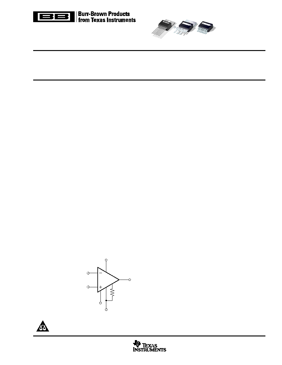
High-Voltage, High-Current
OPERATIONAL AMPLIFIER
DESCRIPTION
The OPA547 is a low-cost, high-voltage/high-current opera-
tional amplifier ideal for driving a wide variety of loads. A
laser-trimmed monolithic integrated circuit provides excellent
low-level signal accuracy and high output voltage and cur-
rent.
The OPA547 operates from either single or dual supplies for
design flexibility. In single-supply operation, the input com-
mon-mode range extends below ground.
The OPA547 is internally protected against over-temperature
conditions and current overloads. In addition, the OPA547
was designed to provide an accurate, user-selected current
limit. Unlike other designs which use a "power" resistor in
series with the output current path, the OPA547 senses the
load indirectly. This allows the current limit to be adjusted
from 0mA to 750mA with a 0 to 150
µ
A control signal. This is
easily done with a resistor/potentiometer or controlled digi-
tally with a voltage-out or current-out DAC.
The Enable/Status (E/S) pin provides two functions. An input
on the pin not only disables the output stage to effectively
disconnect the load, but also reduces the quiescent current
to conserve power. The E/S pin output can be monitored to
determine if the OPA547 is in thermal shutdown.
The OPA547 is available in an industry-standard
7-lead staggered and straight lead TO-220 package, and a
7-lead DDPAK surface-mount plastic power package. The
copper tab allows easy mounting to a heat sink or circuit
board for excellent thermal performance. It is specified for
operation over the extended industrial temperature range,
≠40
∞
C to +85
∞
C.
FEATURES
q
WIDE SUPPLY RANGE
Single Supply: +8V to +60V
Dual Supply:
±
4V to
±
30V
q
HIGH OUTPUT CURRENT:
500mA Continuous
q
WIDE OUTPUT VOLTAGE SWING
q
FULLY PROTECTED:
Thermal Shutdown
Adjustable Current Limit
q
OUTPUT DISABLE CONTROL
q
THERMAL SHUTDOWN INDICATOR
q
HIGH SLEW RATE: 6V/
µ
s
q
LOW QUIESCENT CURRENT
q
PACKAGES:
7-Lead TO-220, Zip and Straight Leads
7-Lead DDPAK Surface-Mount
APPLICATIONS
q
VALVE, ACTUATOR DRIVERS
q
SYNCHRO, SERVO DRIVERS
q
POWER SUPPLIES
q
TEST EQUIPMENT
q
TRANSDUCER EXCITATION
q
AUDIO AMPLIFIERS
OPA547
V
IN
≠
V
IN
+
V+
E/S
R
CL
R
CL
sets the current limit
value from 0 to 750mA.
(0.25W
Signal Resistor)
I
LIM
V
O
V≠
OPA547
SBOS056D ≠ JANUARY 2002 ≠ OCTOBER 2003
www.ti.com
PRODUCTION DATA information is current as of publication date.
Products conform to specifications per the terms of Texas Instruments
standard warranty. Production processing does not necessarily include
testing of all parameters.
Copyright © 2002-2003, Texas Instruments Incorporated
Please be aware that an important notice concerning availability, standard warranty, and use in critical applications of
Texas Instruments semiconductor products and disclaimers thereto appears at the end of this data sheet.
OPA5
47
OPA
547
OPA5
47
OPA547
2
SBOS056D
www.ti.com
ABSOLUTE MAXIMUM RATINGS
(1)
Output Current ................................................................. See SOA Curve
Supply Voltage, V+ to V≠ ................................................................... 60V
Input Voltage .................................................. (V≠) ≠ 0.5V to (V+) + 0.5V
Input Shutdown Voltage ........................................................................ V+
Operating Temperature .................................................. ≠40
∞
C to +125
∞
C
Storage Temperature ..................................................... ≠55
∞
C to +125
∞
C
Junction Temperature ...................................................................... 150
∞
C
Lead Temperature (soldering 10s)
(2)
.............................................. 300
∞
C
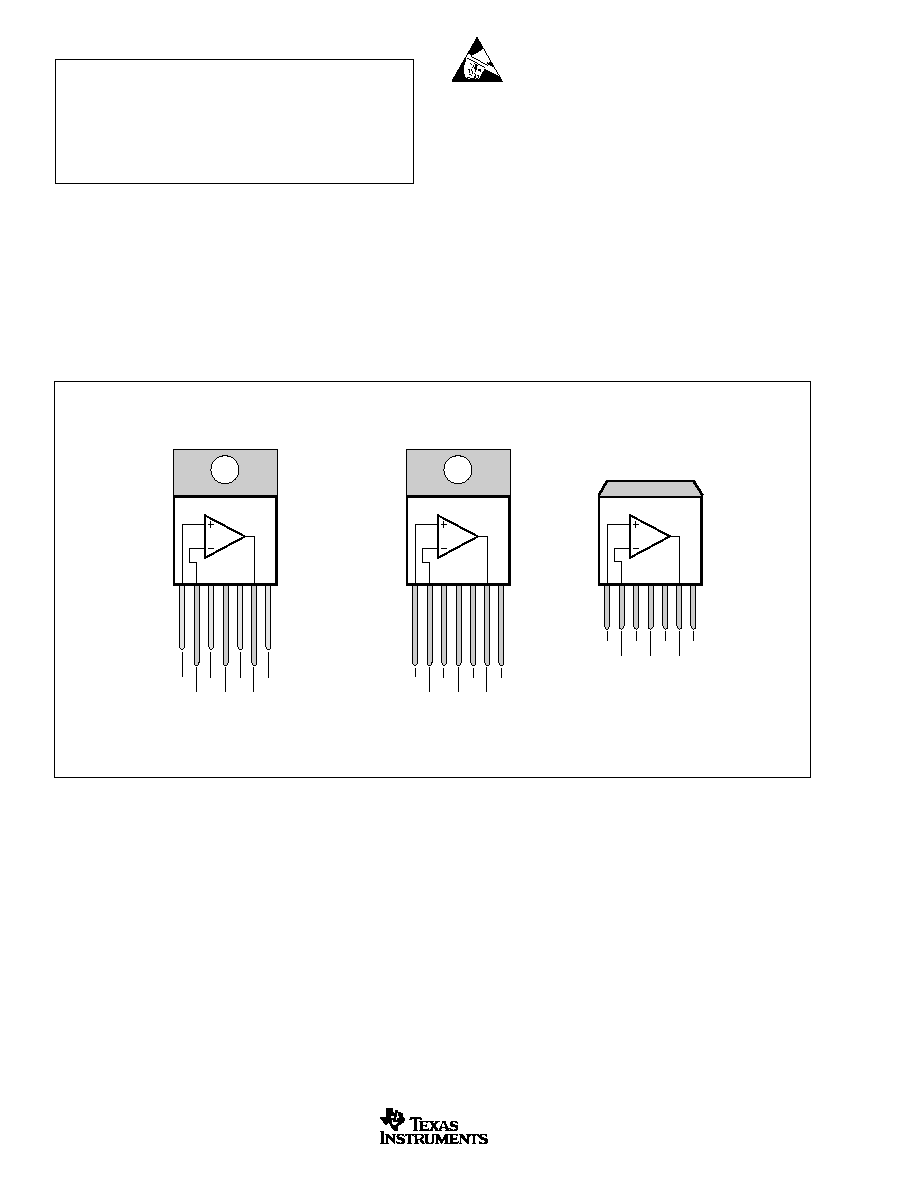
Top Front View
PIN CONFIGURATIONS
NOTES: (1) Stresses above these ratings may cause permanent damage. (2)
Vapor-phase or IR reflow techniques are recommended for soldering the
OPA547F surface-mount package. Wave soldering is not recommended due to
excessive thermal shock and "shadowing" of nearby devices.
PACKAGE/ORDERING INFORMATION
For the most current package and ordering information, see the Package Ordering Addendum at the end of this data sheet.
ELECTROSTATIC
DISCHARGE SENSITIVITY
This integrated circuit can be damaged by ESD. Texas Instru-
ments recommends that all integrated circuits be handled with
appropriate precautions. Failure to observe proper handling
and installation procedures can cause damage.
ESD damage can range from subtle performance degradation
to complete device failure. Precision integrated circuits may be
more susceptible to damage because very small parametric
changes could cause the device not to meet its published
specifications.
7-Lead
Straight-Formed
TO-220 (T-1)
NOTE: Tabs are electrically connected to the V≠ supply.
I
LIM
V≠
V
O
V+
V
IN≠
V
IN+
1 2 3 4 5 6
E/S
7
7-Lead
DDPAK (FA)
Surface-Mount
I
LIM
V≠
V
O
V+
V
IN≠
V
IN+
1 2 3 4 5 6
E/S
7
7-Lead
Stagger-Formed
TO-220 (T)
I
LIM
V≠
V
O
V+
V
IN≠
V
IN+
1 2 3 4 5 6
E/S
7

OPA547
3
SBOS056D
www.ti.com
ELECTRICAL CHARACTERISTICS
At T
CASE
= +25
∞
C, V
S
=
±
30V and E/S pin open, unless otherwise noted.
OPA547T, F
PARAMETER
CONDITION
MIN
TYP
MAX
UNITS
OFFSET VOLTAGE
Input Offset Voltage
V
CM
= 0, I
O
= 0
±
1
±
5
mV
vs Temperature
T
A
= ≠40
∞
C to +85
∞
C
±
25
µ
V/
∞
C
vs Power Supply
V
S
=
±
4V to
±
30V
10
100
µ
V/V
INPUT BIAS CURRENT
(1)
Input Bias Current
(2)
V
CM
= 0V
≠100
≠500
nA
vs Temperature
±
0.5
nA/
∞
C
Input Offset Current
V
CM
= 0V
±
5
±
50
nA
NOISE
Input Voltage Noise Density, f = 1kHz
90
nV/
Hz
Current Noise Density, f = 1kHz
200
fA/
Hz
INPUT VOLTAGE RANGE
Common-Mode Voltage Range: Positive
Linear Operation
(V+) ≠3
(V+) ≠2.3
V
Negative
Linear Operation
(V≠) ≠0.1
(V≠) ≠0.2
V
Common-Mode Rejection
V
CM
= (V≠) ≠0.1V to (V+) ≠3V
80
95
dB
INPUT IMPEDANCE
Differential
10
7
|| 6
|| pF
Common-Mode
10
9
|| 4
|| pF
OPEN-LOOP GAIN
Open-Loop Voltage Gain, f = 10Hz
V
O
=
±
25V, R
L
= 1k
100
115
dB
V
O
=
±
25V, R
L
= 50
110
dB
FREQUENCY RESPONSE
Gain-Bandwidth Product
R
L
= 50
1
MHz
Slew Rate
G = 1, 50Vp-p, R
L
= 50
6
V/
µ
s
Full-Power Bandwidth
See Typical Curve
kHz
Settling Time:
±
0.1%
G = ≠10, 50V Step
18
µ
s
Total Harmonic Distortion + Noise, f = 1kHz
R
L
= 50
, G = +3V, 1W Power
0.004
(3)
%
OUTPUT
Voltage Output, Positive
I
O
= 0.5A
(V+) ≠2.2
(V+) ≠1.9
V
Negative
I
O
= ≠0.5A
(V≠) +1.6
(V≠) +1.3
V
Positive
I
O
= 0.1A
(V+) ≠1.8
(V+) ≠1.5
V
Negative
I
O
= ≠0.1A
(V≠) +1.2
(V≠) +0.8
V
Maximum Continuous Current Output: dc
±
500
mA
ac
500
mArms
Leakage Current, Output Disabled, dc
See Typical Curve
Output Current Limit
Current Limit Range
0 to
±
750
mA
Current Limit Equation
I
LIM
= (5000)(4.75)/(31600
+ R
CL
)
A
Current Limit Tolerance
(1)
R
CL
= 31.6k
(I
LIM
=
±
375mA),
±
10
±
30
mA
R
L
= 50
Capacitive Load Drive
See Typical Curve
(4)
OUTPUT ENABLE /STATUS (E/S) PIN
Shutdown Input Mode
V
E/S
HIGH (output enabled)
E/S Pin Open or Forced HIGH
(V≠) +2.4
V
V
E/S
LOW (output disabled)
E/S Pin Forced LOW
(V≠) +0.8
V
I
E/S
HIGH (output enabled)
E/S Pin HIGH
≠60
µ
A
I
E/S
LOW (output disabled)
E/S Pin LOW
≠65
µ
A
Output Disable Time
1
µ
s
Output Enable Time
3
ms
Thermal Shutdown Status Output
Normal Operation
Sourcing 20
µ
A
(V≠) +2.4
(V≠) +3.5
V
Thermally Shutdown
Sinking 5
µ
A, T
J
> 160
∞
C
(V≠) +0.35
(V≠) +0.8
V
Junction Temperature, Shutdown
+160
∞
C
Reset from Shutdown
+140
∞
C
POWER SUPPLY
Specified Voltage
±
30
V
Operating Voltage Range
±
4
±
30
V
Quiescent Current
I
LIM
Connected to V≠, I
O
= 0
±
10
±
15
mA
Quiescent Current, Shutdown Mode
I
LIM
Connected to V≠
±
4
mA
TEMPERATURE RANGE
Specified Range
≠40
+85
∞
C
Operating Range
≠40
+125
∞
C
Storage Range
≠55
+125
∞
C
Thermal Resistance,
JC
7-Lead DDPAK, 7-Lead TO-220
f > 50Hz
2
∞
C/W
7-Lead DDPAK, 7-Lead TO-220
dc
3
∞
C/W
Thermal Resistance,
JA
7-Lead DDPAK, 7-Lead TO-220
No Heat Sink
65
∞
C/W
NOTES: (1) High-speed test at T
J
= +25
∞
C. (2) Positive conventional current flows into the input terminals. (3) See "Total Harmonic Distortion+Noise" in the Typical
Characteristics section for additional power levels. (4) See "Small-Signal Overshoot vs Load Capacitance" in the Typical Characteristics section.
OPA547
4
SBOS056D
www.ti.com
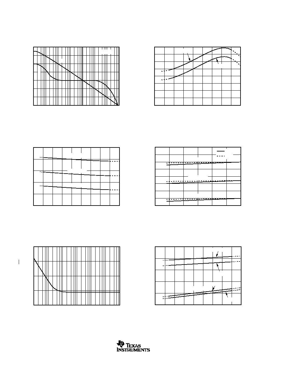
TYPICAL CHARACTERISTICS
At T
CASE
= +25
∞
C, V
S
=
±
30V, and E/S pin open, unless otherwise noted.
1
10
100
1k
10k
100k
1M
10M
120
100
80
60
40
20
0
≠20
Gain (dB)
0
≠45
≠90
≠135
≠180
Phase (
∞
)
Frequency (Hz)
OPEN-LOOP GAIN AND PHASE
vs FREQUENCY
R
L
= 50
G
≠75
≠50
≠25
0
25
50
75
100
125
150
≠160
≠140
≠120
≠100
≠80
≠60
≠40
≠20
0
Input Bias Current (nA)
Temperature (
∞
C)
INPUT BIAS CURRENT vs TEMPERATURE
I
B
V
S
=
±
5V
V
S
=
±
30V
≠75
≠50
≠25
0
25
50
75
100
125
150
±
600
±
500
±
400
±
300
±
200
±
100
Current Limit (mA)
Temperature (
∞
C)
CURRENT LIMIT vs TEMPERATURE
R
CL
= 31.6k
R
CL
= 63.4k
R
CL
= 15.9k
0
±
5
±
10
±
15
±
20
±
25
±
30
±
600
±
550
±
500
±
450
+400
±
350
±
300
±
250
±
200
Current Limit (mA)
Supply Voltage (V)
CURRENT LIMIT vs SUPPLY VOLTAGE
R
CL
= 15.9k
R
CL
= 31.6k
R
CL
= 63.4k
+I
LIM
≠I
LIM
1
10
100
1k
10k
100k
1M
400
300
200
100
0
Voltage Noise (nV/
Hz)
Frequency (Hz)
VOLTAGE NOISE DENSITY vs FREQUENCY
≠75
≠50
≠25
0
25
50
75
100
125
150
±
12
±
10
±
8
±
6
±
4
±
2
Quiescent Current (mA)
Temperature (
∞
C)
QUIESCENT CURRENT vs TEMPERATURE
I
Q
I
Q
Shutdown
V
S
=
±
30V
V
S
=
±
5V
V
S
=
±
30V
V
S
=
±
5V
OPA547
5
SBOS056D
www.ti.com
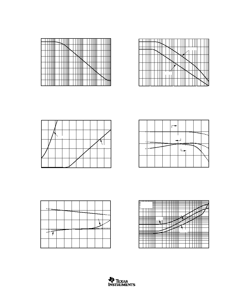
TYPICAL CHARACTERISTICS
(Cont.)
At T
CASE
= +25
∞
C, V
S
=
±
30V, and E/S pin open, unless otherwise noted.
10
100
1k
10k
100k
1M
100
90
80
70
60
50
40
30
20
CMR (dB)
Frequency (Hz)
COMMON-MODE REJECTION vs FREQUENCY
1
10
100
1k
10k
100k
1M
120
100
80
60
40
20
0
PSR (dB)
Frequency (Hz)
POWER SUPPLY REJECTION
vs FREQUENCY
+PSRR
≠PSRR
0
2k
4k
6k
8k
10k
12k
14k
16k
18k
20k
50
40
3
20
10
0
Overshoot (%)
Load Capacitance (pF)
SMALL-SIGNAL OVERSHOOT
vs LOAD CAPACITANCE
G = ≠1
G = +1
≠75
≠50
≠25
0
A
OL
25
50
75
100
125
150
105
100
95
90
85
CMRR (dB)
120
115
100
95
90
PSRR, A
OL
(dB)
Temperature (
∞
C)
OPEN-LOOP GAIN, COMMON-MODE REJECTION,
AND POWER SUPPLY REJECTION vs TEMPERATURE
CMRR
PSRR
≠75
≠50
≠25
0
25
50
75
100
125
150
1.25
1
0.75
0.5
0.25
0
7.5
7
6.5
6
5.5
5
Gain-Bandwidth Product (MHz)
Slew Rate (V/
µ
s)
Temperature (
∞
C)
GAIN-BANDWIDTH PRODUCT AND
SLEW RATE vs TEMPERATURE
SR+
SR≠
GBW
20
100
1k
10k
20k
0.1
0.01
0.001
0.0001
THD+N (%)
Frequency (Hz)
TOTAL HARMONIC DISTORTION+NOISE
vs FREQUENCY
R
L
= 50
G = +3
0.1W
1W
6.25W