
OPA
567
OPA567
Rail-to-Rail I/O, 2A
POWER AMPLIFIER
DESCRIPTION
The OPA567 is a low-cost, high-current, operational amplifier
designed for driving a wide variety of loads while operating on
low-voltage supplies. It operates from either single or dual
supplies for design flexibility and has rail-to-rail swing on the
input and output. Output swing is within 300mV of the supply
rails, with output current of 2A. Smaller loads allow an output
swing closer to the rails.
The OPA567 is unity gain stable, easy to use, and free from
the phase inversion problems found in some power amplifi-
ers. High performance is maintained at voltage swings near
the output rails.
The OPA567 provides an accurate user-selected current
limit set with an external resistor, or digitally adjusted via a
Digital-to-Analog Converter (DAC).
The output of the OPA567 can be independently disabled
using the Enable pin. This feature saves power and protects
the load.
Two flags are provided. The current limit flag, I
FLAG
, warns of
current limit conditions. T
FLAG
is a thermal flag that warns of
thermal overstress. The T
FLAG
pin can be connected to the
Enable pin to provide a thermal shutdown solution.
The OPA567 is available in a tiny 5mm x 5mm Quad
Flatpack No-lead (QFN) package and features an exposed
thermal pad that enhances thermal and electrical character-
istics. It is small and easy to heat sink. The OPA567 is
specified for operation over the industrial temperature range,
�40
�
C to +85
�
C.
FEATURES
q
HIGH OUTPUT CURRENT: 2A
q
OUTPUT SWINGS TO: 150mV of Rails with I
O
= 2A
q
THERMAL PROTECTION
q
ADJUSTABLE CURRENT LIMIT
q
TWO FLAGS: Current Limit and Temperature
Warning
q
LOW SUPPLY VOLTAGE OPERATION: 2.7V to 5.5V
q
SHUTDOWN FUNCTION WITH OUTPUT DISABLE
q
SMALL POWER PACKAGE
APPLICATIONS
q
THERMOELECTRIC COOLER DRIVER
q
LASER DIODE PUMP DRIVER
q
VALVE, ACTUATOR DRIVER
q
SYNCHRO, SERVO DRIVER
q
TRANSDUCER EXCITATION
q
GENERAL LINEAR POWER BOOSTER FOR
OP AMPS
www.ti.com
Copyright � 2005, Texas Instruments Incorporated
SBOS287A � JUNE 2005 � REVISED SEPTEMBER 2005
OPA567
T
FLAG
V�
V
O
NOTE: (1) Connect
for thermal protection.
�IN
+IN
V+
8
1, 12
4, 5
10
11
7
2, 3
6
9
R
SET
(1)
Enable
I
SET
I
FLAG
Please be aware that an important notice concerning availability, standard warranty, and use in critical applications of
Texas Instruments semiconductor products and disclaimers thereto appears at the end of this data sheet.
PowerPAD is a trademark of Texas Instruments. All other trademarks are the property of their respective owners.
OPA567 RELATED PRODUCTS
FEATURES
PRODUCT
Same features as the OPA567, plus current
OPA569
monitor output and paralleling ability in SO-20
PowerPADTM package.
PRODUCTION DATA information is current as of publication date.
Products conform to specifications per the terms of Texas Instruments
standard warranty. Production processing does not necessarily include
testing of all parameters.
OPA567
SBOS287A
2
www.ti.com
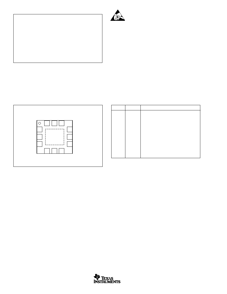
PIN #
NAME
DESCRIPTION
1, 12
V+
Positive Power-Supply Voltage
2, 3
V
O
Output
4, 5
V�
Negative Power-Supply Voltage
6
I
SET
Current Limit Set Pin
(1)
7
I
FLAG
Current Limit Flag--Indicates when part is in
current limit (active LOW).
8
�IN
Inverting Input
9
+IN
Noninverting Input
10
T
FLAG
Thermal Flag--Indicates thermal stress (active
LOW).
11
ENABLE
Enabled HIGH, shut down LOW.
ELECTROSTATIC
DISCHARGE SENSITIVITY
This integrated circuit can be damaged by ESD. Texas
Instruments recommends that all integrated circuits be handled
with appropriate precautions. Failure to observe proper han-
dling and installation procedures can cause damage.
ESD damage can range from subtle performance degrada-
tion to complete device failure. Precision integrated circuits
may be more susceptible to damage because very small
parametric changes could cause the device not to meet its
published specifications.
Supply Voltage ................................................................................. +7.5V
Output Current ............................................................... See SOA Curves
Signal Input Terminals (pins 8 and 9):
Voltage
(2)
............................................... (V�) � 0.5V to (V+) + 0.5V
Current
(2)
................................................................................
�
10mA
Output Short-Circuit
(3)
........ Continuous when thermal protection enabled
Enable Pin (pin 11) ........................................ (V�) � 0.5V to (V�) + 7.5V
Current Limit Set, I
LIMIT
Pin (pin 6) ................ (V�) � 0.5V to (V+) + 0.5V
Operating Temperature .................................................. �55
�
C to +125
�
C
Storage Temperature ..................................................... �65
�
C to +150
�
C
Junction Temperature .................................................................... +150
�
C
ESD Rating:
Human Body Model ................................................................... 3kV
Charged Device Model .......................................................... 1500V
NOTES: (1) Stresses above these ratings may cause permanent damage.
Exposure to absolute maximum conditions for extended periods may de-
grade device reliability. These are stress ratings only, and functional opera-
tion of the device at these or any other conditions beyond those specified is
not implied. (2) Input terminals are diode-clamped to the power-supply rails.
Input signals that can swing more than 0.5V beyond the supply rails should
be current limited to 10mA or less. (3) Short-circuit to ground.
PIN CONFIGURATION
ABSOLUTE MAXIMUM RATINGS
(1)
V+
V
O
V
O
+IN
�IN
I
FLAG
1
2
3
9
8
7
Metal
heat sink
(located
on bottom)
V+
Enable
T
FLAG
12
11
10
V
�
V
�
I
SET
4
5
6
Top View
QFN
PIN DESCRIPTIONS
NOTE: (1) This pin limits the output current. The limited value, I
LIMIT
, is
9800(I
SET
), where I
SET
is the current flowing through the I
SET
pin. This current
is programmed by the resistor R
SET
connected to V�.
PACKAGE/ORDERING INFORMATION
For the most current package and ordering information, see
the Package Option Addendum located at the end of this
data sheet.

OPA567
SBOS287A
3
www.ti.com
ELECTRICAL CHARACTERISTICS: V
S
= +2.7V to +5.5V
Boldface limits apply over the specified temperature range, T
A
= �40
�
C to +85
�
C.
At T
CASE
= +25
�
C, R
L
= 1k
, and connected to V
S
/ 2, unless otherwise noted.
NOTES:
(1) See typical characteristic,
Maximum Output Voltage vs Frequency.
(2) See typical characteristic,
Total Harmonic Distortion + Noise vs Frequency.
(3) Swing to the rail is measured in final test. Under those conditions, the A
OL
is derived from characterization.
(4) See Safe Operating Area (SOA) plots.
(5) See typical characteristic,
Overshoot vs Load Capacitance.
(6) See the
Typical Characteristics section. Higher frequency output impedance can affect frequency stability.
(7) External current limit setting resistor is required; see Figure 1.
(8) I
LIMIT
is the value of the desired current limit and is equal to 9800(I
SET
), where I
SET
is the current through the I
SET
pin. I
LIMIT
tolerance is proportional to the ratio of
I
LIMIT
/I
SET
. Errors from this parameter can be calibrated out--see the
Applications Information section.
(9) V
SET
is a voltage reference that equals the difference between the voltage of the I
SET
pin and V�, and is referenced to the negative rail. Errors from this parameter
can be calibrated out--see the
Applications Information section.
OPA567
PARAMETER
CONDITION
MIN
TYP
MAX
UNITS
OFFSET VOLTAGE
Input Offset Voltage
V
OS
I
O
= 0V, V
S
= +5V
�
0.5
�
2
mV
vs Temperature
dV
OS
/dT
T
A
= �40
�
C to +85
�
C
�
1.3
�
V/
�
C
vs Power Supply
PSRR
V
S
= +2.7V to +5.5V, V
CM
= (V�) +0.55V
12
60
�
V/V
INPUT BIAS CURRENT
Input Bias Current
I
B
�
1
�
10
pA
vs Temperature
(doubles every 10
�
C)
Input Offset Current
I
OS
�
2
�
10
pA
NOISE
Input Voltage Noise Density, f = 1kHz
e
n
12
nV/
Hz
f = 0.1Hz to 10Hz
8
�
V
PP
Current Noise Density, f = 1kHz
i
n
0.6
fA/
Hz
INPUT VOLTAGE RANGE
Common-Mode Voltage Range
V
CM
Linear Operation
(V�) � 0.1
(V+) + 0.1
V
Common-Mode Rejection Ratio
CMRR
V
S
= +5V, �0.1V < V
CM
< 3.2V
80
100
dB
V
S
= +5V, �0.1V < V
CM
< 5.1V
60
80
dB
INPUT IMPEDANCE
Differential
10
13
|| 4.5
|| pF
Common-Mode
10
13
|| 9
|| pF
OPEN-LOOP GAIN
Open-Loop Voltage Gain
A
OL
0.2V
< V
O
< 4.8V, R
L
= 1k
, V
S
= +5V
100
126
dB
0.3V
< V
O
< 4.7V, R
L
= 1.15
, V
S
= +5V
90
dB
FREQUENCY RESPONSE
Gain Bandwidth Product
GBW
1.2
MHz
Slew Rate
SR
G = +1, V
O
= 4.0V Step
1.2
V/
�
s
Full-Power Bandwidth
(1)
See Typical Characteristics
Settling Time:
�
0.1%
G = �1, V
O
= 4.0V Step
5
�
s
Total Harmonic Distortion + Noise
(2)
THD+N
See Typical Characteristics
OUTPUT
Voltage Output Swing from Rail
V
O
R
L
= 1k
, A
OL
> 100dB
(V�) + 0.2
(V
S
)
�
0.02
(V+) � 0.2
V
I
O
=
�
2A, V
S
= +5V, A
OL
> 80dB
(3)
(V�) + 0.3
(V
S
)
�
0.2
(V+) � 0.3
V
Maximum Continuous Current Output: dc
(4)
2.4
A
Capacitive Load Drive
(5)
C
LOAD
See Typical Characteristics
Closed-Loop Output Impedance
(6)
R
O
G = 1, dc
0.1
G = 1, f = 10kHz
0.44
G = 1, f = 1.2MHz
45
Output Disabled Output Impedance
12M || 570
|| pF
CURRENT LIMIT (I
SET
Pin)
Output Current Limit
(7)
Externally Adjustable
�
0.2 to
�
2.2
A
Current Limit Equation
(8)
I
LIMIT
= I
SET
� 9800
A
R
SET
Equation
R
SET
= 9800 (1.18V/I
LIMIT
)
Current Limit Tolerance
(8)
, Positive
I
LIMIT
= 1A
�
3
�
10
%
Negative
I
LIMIT
= 1A
�
3
�
15
%
V
SET
Tolerance
(9)
(V�) + 1.05
(V�) + 1.18
(V�) + 1.3
V
ENABLE/SHUTDOWN INPUT
Enable Pin Bias Current
V
SD
= 0V
0.2
�
A
HIGH (Output enabled)
V
SD
Pin Open or Forced HIGH
(V�) + 2.5
V
LOW (Output disabled)
V
SD
Pin Forced LOW
(V�) + 0.8
V
Output Disable Time
R
L
= 1
0.5
�
s
Output Enable Time
R
L
= 1
15
�
s

OPA567
SBOS287A
4
www.ti.com
THERMAL FLAG PIN (T
FLAG
)
Junction Temperature:
T
J
Alarm (thermal status pin Low)
Thermal overstress
+147
�
C
Return to normal operation (Thermal Flag pin High)
Normal operation
+130
�
C
Thermal Flag Pin Voltage
During normal operation
T
FLAG
pin sourcing 25
�
A
(V+) � 0.8V
V+
V
During thermal overstress
T
FLAG
pin sinking 25
�
A
V�
(V�) + 0.8
V
CURRENT LIMIT FLAG PIN (I
FLAG
)
Current Limit Flag Pin Voltage
During normal operation
I
FLAG
pin sourcing 25
�
A
(V+) � 0.8V
V+
V
During current limit
I
FLAG
pin sinking 25
�
A
V�
(V�) + 0.8
V
POWER SUPPLY
Specified Voltage Range
V
S
+2.7
+5.5
V
Operating Voltage Range
+2.5
+5.5
V
Quiescent Current
(10)
I
Q
I
O
= 0, I
LIMIT
= 200mA, V
S
= 5V
+3.4
+6
mA
I
O
= 0, I
LIMIT
= 2A, V
S
= 5V
+9
+11
mA
Quiescent Current in Shutdown Mode
I
O
= 0, V
SD
= 0.8V, V
S
= 5V
+0.01
mA
TEMPERATURE RANGE
Specified Range
Junction Temperature
�40
+85
�
C
Operating Range
Junction Temperature
�55
+125
�
C
Storage Range
�65
+150
�
C
Thermal Resistance: Junction-to-Case
JC
6
�
C/W
Junction-to-Ambient
JA
38
�
C/W
ELECTRICAL CHARACTERISTICS: V
S
= +2.7V to +5.5V
(Cont.)
Boldface limits apply over the specified temperature range, T
A
= �40
�
C to +85
�
C.
At T
CASE
= +25
�
C, R
L
= 1k
, and connected to V
S
/ 2, unless otherwise noted.
OPA567
PARAMETER
CONDITION
MIN
TYP
MAX
UNITS
NOTES: (10) Quiescent current is a function of the current limit setting. See
Adjustable Current Limit and Current Limit Flag Pin in the Applications Information section.
OPA567
SBOS287A
5
www.ti.com
TYPICAL CHARACTERISTICS
At T
A
= +25
�
C, V
S
= +5V, unless otherwise noted.
180
160
140
120
100
80
60
40
20
0
�20
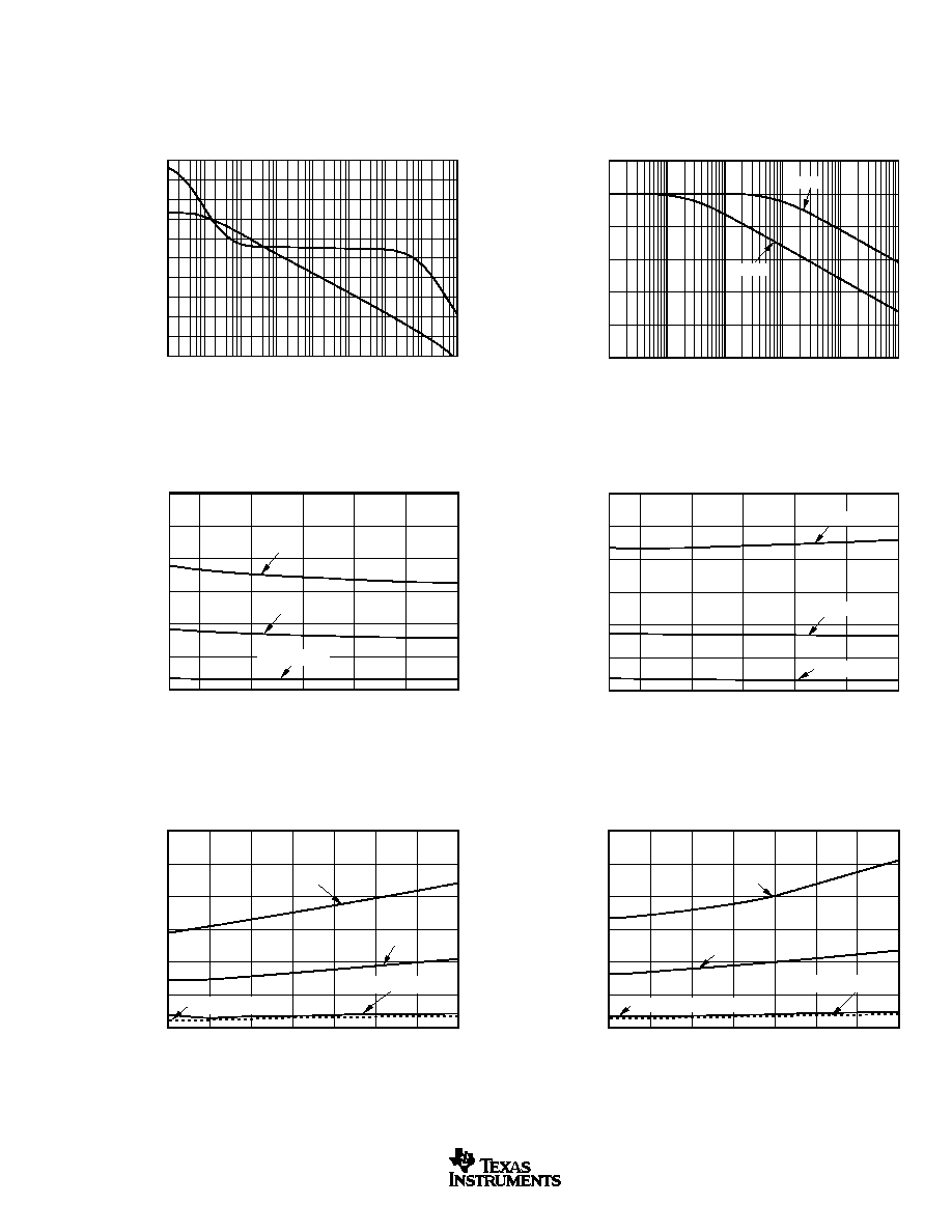
OPEN-LOOP GAIN AND PHASE vs FREQUENCY
Frequency (Hz)
1
10
100
1k
10k
100k
10M
1M
0.1
0
�20
�40
�60
�80
�100
�120
�140
�160
�180
�200
Phase (
�
)
A
OL
(dB)
120
100
80
60
40
20
0
POWER-SUPPLY AND COMMON-MODE
REJECTION RATIO vs FREQUENCY
Frequency (Hz)
PSRR and CMRR (dB)
1
10
100
1k
10k
100k
CMRR
PSRR
300
250
200
150
100
50
0
OUTPUT SWING TO POSITIVE RAIL
vs SUPPLY VOLTAGE
Supply Voltage (V)
Swing to Rail (mV)
2.7
3.0
3.5
4.0
4.5
5.0
5.5
I
OUT
= 200mA
I
OUT
= 2A
I
OUT
= 1A
300
250
200
150
100
50
0
OUTPUT SWING TO NEGATIVE RAIL
vs SUPPLY VOLTAGE
Supply Voltage (V)
Swing to Rail (mV)
2.7
3.0
3.5
4.0
4.5
5.0
5.5
I
OUT
= �200mA
I
OUT
= �2A
I
OUT
= �1A
300
250
200
150
100
50
0
OUTPUT SWING TO POSITIVE RAIL
vs TEMPERATURE
Temperature (
�
C)
Swing to Rail (mV)
�55
�35
�15
5
25
45
65
85
I
O
= 2A
V
S
= 2.7V, I
O
= 200mA
I
O
= 1A
V
S
= 5V, I
O
= 200mA
300
250
200
150
100
50
0
OUTPUT SWING TO NEGATIVE RAIL
vs TEMPERATURE
Temperature (
�
C)
Swing to Rail (mV)
�55
�35
�15
5
25
45
65
85
I
O
= 2A
V
S
= 5V, I
O
= 200mA
I
O
= 1A
V
S
= 2.7V, I
O
= 200mA

OPA567
SBOS287A
6
www.ti.com
TYPICAL CHARACTERISTICS
(Cont.)
At T
A
= +25
�
C, V
S
= +5V, unless otherwise noted.
1000
100
10
1
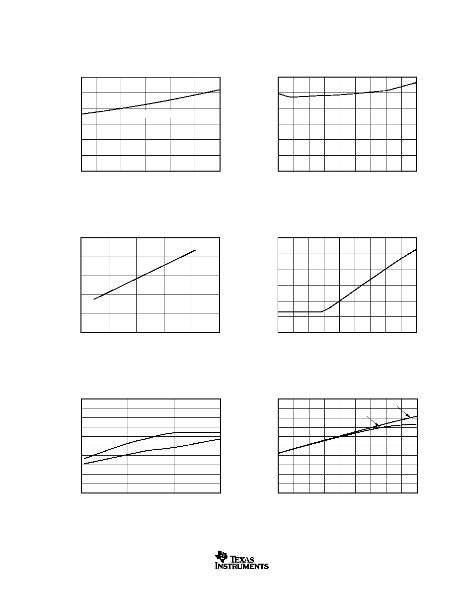
INPUT VOLTAGE NOISE SPECTRAL DENSITY
vs FREQUENCY
Frequency (Hz)
Input Voltage Noise (nV
Hz)
10
100
1k
10k
100k
0.1Hz TO 10Hz INPUT VOLTAGE NOISE
1
�
V/div
1s/div
6
5
4
3
2
1
0
MAXIMUM OUTPUT VOLTAGE vs FREQUENCY
Frequency (Hz)
Output Voltage (V
PP
)
100
1k
100k
10k
1M
V
S
= 5V
R
L
= 1k
R
L
= 1
R
L
= 1k
V
S
= 2.7V
R
L
= 1
10
1
0.1
0.01
0.001
TOTAL HARMONIC DISTORTION+NOISE
vs FREQUENCY
Frequency (Hz)
THD+N (%)
20
100
1k
10k 20k
R
L
= 2
R
L
= 8
R
L
= 1k
10
8
6
4
2
0
QUIESCENT CURRENT vs SUPPLY VOLTAGE
Supply Voltage (V)
Quiescent Current (mA)
2.7
3.0
3.5
4.0
4.5
5.0
5.5
Current Limit = 1A
Current Limit = 2A
Current Limit = 200mA
10
8
6
4
2
0
QUIESCENT CURRENT vs TEMPERATURE
Temperature (
�
C)
Quiescent Current (mA)
�55
�35
5
�15
25
45
65
105
85
125
I
Q
(I
LIMIT
= 2A)
I
Q
(I
LIMIT
= 200mA)
OPA567
SBOS287A
7
www.ti.com
TYPICAL CHARACTERISTICS
(Cont.)
At T
A
= +25
�
C, V
S
= +5V, unless otherwise noted.
12
10
8
6
4
2
0
SHUTDOWN CURRENT vs SUPPLY VOLTAGE
Supply Voltage (V)
Shutdown Current (
�
A)
2.7
3.0
3.5
4.0
4.5
5.0
5.5
I
LIMIT
= 200mA, 1A, and 2A
SHUTDOWN CURRENT vs TEMPERATURE
Temperature (
�
C)
Shutdown Current (
�
A)
12
10
8
6
4
2
0
�55
�35
5
�15
25
45
65
105
85
125
10
8
6
4
2
0
QUIESCENT CURRENT vs CURRENT LIMIT SETTING
Current Limit Setting (A)
Quiescent Current (mA)
0
0.5
1.0
1.5
2.0
2.5
10000
1000
100
10
1
0.1
0.01
INPUT BIAS CURRENT vs TEMPERATURE
Temperature (
�
C)
Input Bias Current
(pA)
�55
�35
�15
5
25
45
65
85
105
125
2.0
1.8
1.6
1.4
1.2
1.0
0.8
0.6
0.4
0.2
0
SLEW RATE vs LOAD RESISTANCE
Load Resistance (
)
Slew Rate (V/
�
s)
1
10
SR�
SR+
100
1000
2.0
1.8
1.6
1.4
1.2
1.0
0.8
0.6
0.4
0.2
0
SLEW RATE vs TEMPERATURE
Temperature (
�
C)
Slew Rate (V/
�
s)
�55
5
25
45
�35
�15
65
85
105
125
SR�
SR+
OPA567
SBOS287A
8
www.ti.com
TYPICAL CHARACTERISTICS
(Cont.)
At T
A
= +25
�
C, V
S
= +5V, unless otherwise noted.
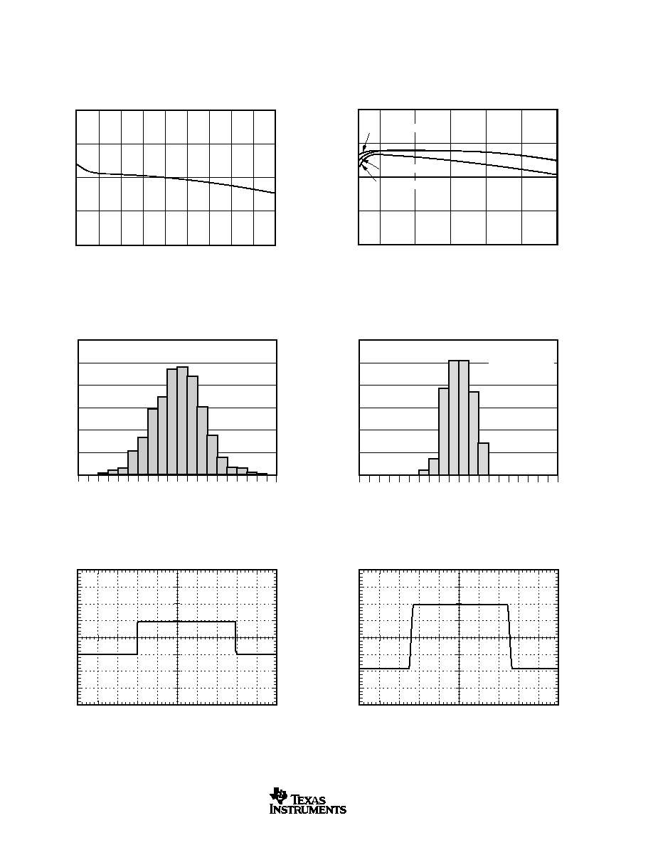
1.20
1.19
1.18
1.17
1.16
VOLTAGE ON I
SET
PIN vs TEMPERATURE
Temperature (
�
C)
[V
SET
�
(V
�
)] (V)
�55
�35
�15
5
65
85
105
25
45
125
1.25
1.20
1.15
1.10
1.05
VOLTAGE ON I
SET
PIN vs SUPPLY VOLTAGE
Supply Voltage (V)
[V
SET
�
(V
�
)]
2.7
3.0
3.5
4.0
4.5
5.0
5.5
Current Limit = 1A
Current Limit = 2A
Current Limit = 200mA
OFFSET VOLTAGE
PRODUCTION DISTRIBUTION
V
OS
(mV)
�
2.0
�
1.8
�
1.6
�
1.4
�
1.2
�
1.0
Population
�
0.8
�
0.6
�
0.4
�
0.2
0
0.2
0.4
0.6
0.8
1.0
1.2
1.4
1.6
1.8
2.0
OFFSET VOLTAGE DRIFT
PRODUCTION DISTRIBUTION
Population
Drift (
�
V/
�
C)
�
10
�
9
�
8
�
7
�
6
�
5
�
4
�
3
�
2
�
1
0
1
2
3
4
5
6
7
8
9
10
Typical Production
Distribution of
Packaged Units.
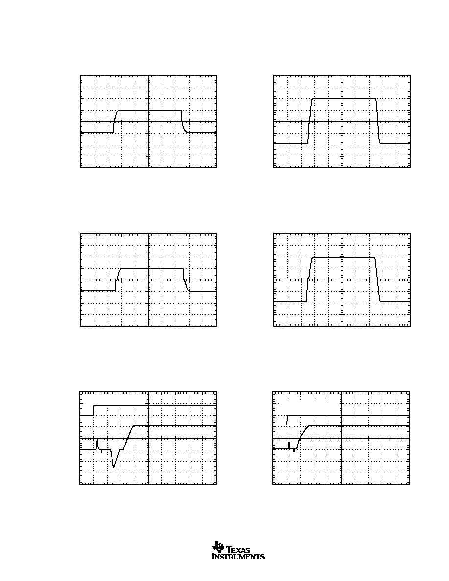
SMALL-SIGNAL STEP RESPONSE
(G = +1, R
L
= 1k
)
50mV/div
10
�
s/div
LARGE-SIGNAL STEP RESPONSE
(G = +1, R
L
= 1k
)
1V/div
20
�
s/div
OPA567
SBOS287A
9
www.ti.com
TYPICAL CHARACTERISTICS
(Cont.)
At T
A
= +25
�
C, V
S
= +5V, unless otherwise noted.
SMALL-SIGNAL STEP RESPONSE
(G = +1, R
L
= 10
)
50mV/div
10
�
s/div
LARGE-SIGNAL STEP RESPONSE
(G = +1, R
L
= 10
)
1V/div
20
�
s/div
SMALL-SIGNAL STEP RESPONSE
(G = +1, R
L
= 1
)
50mV/div
20
�
s/div
LARGE-SIGNAL STEP RESPONSE
(G = +1, R
L
= 1
)
1V/div
20
�
s/div
ENABLE
(10
Load)
2V/div
1V/div
4
�
s/div
Enable/Disable 0.8 to 2.5V
Above Negative Supply
Output Driven to +2V
ENABLE
(1
Load)
10
�
s/div
Enable/Disable 0.8 to 2.5V
Above Negative Supply
Output Driven to +2V
1V/div
2V/div
OPA567
SBOS287A
10
www.ti.com
TYPICAL CHARACTERISTICS
(Cont.)
At T
A
= +25
�
C, V
S
= +5V, unless otherwise noted.
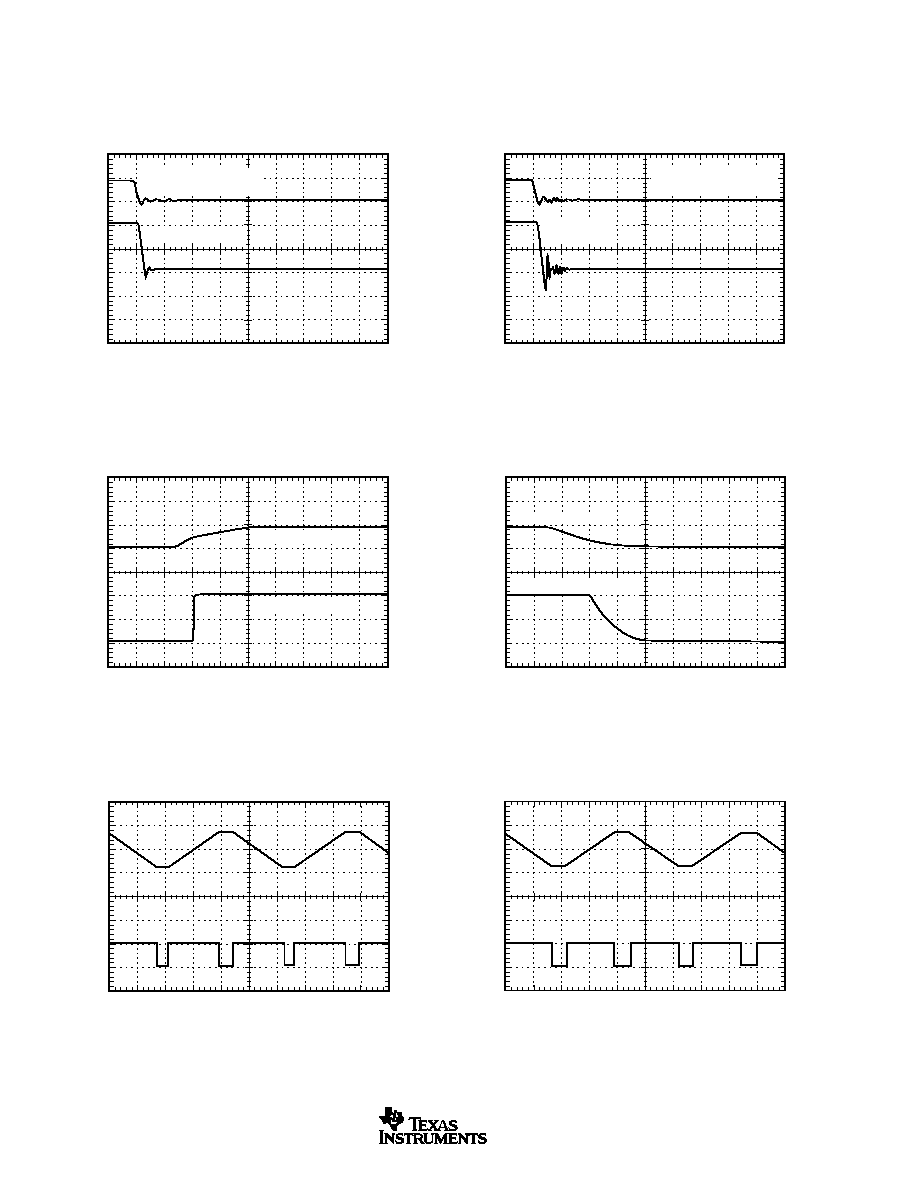
DISABLE
(10
Load)
200ns/div
Enable/Disable 0.8 to 2.5V
Above Negative Supply
Output Driven to +2V
2V/div
1V/div
DISABLE
(1
Load)
200ns/div
Enable/Disable 0.8 to 2.5V
Above Negative Supply
Output Driven
to +2V
2V/div
1V/div
POWER ON
(1
Load)
1ms/div
Output Driven to +2V
Supply 0V to 5V
5V/div
1V/div
POWER OFF
(1
Load)
1ms/div
1V/div
5V/div
Output Driven to +2V
Supply 5V to 0V
IN AND OUT OF CURRENT LIMIT TRANSIENT
(R
L
= 0.75
, Current Limit = 2A)
V
OUT
(2V/div)
Current Limit Flag
(5V/div)
200
�
s/div
IN AND OUT OF CURRENT LIMIT TRANSIENT
(R
L
= 7.5
, Current Limit = 200mA)
V
OUT
(2V/div)
Current Limit Flag
(5V/div)
200
�
s/div
OPA567
SBOS287A
11
www.ti.com
TYPICAL CHARACTERISTICS
(Cont.)
At T
A
= +25
�
C, V
S
= +5V, unless otherwise noted.
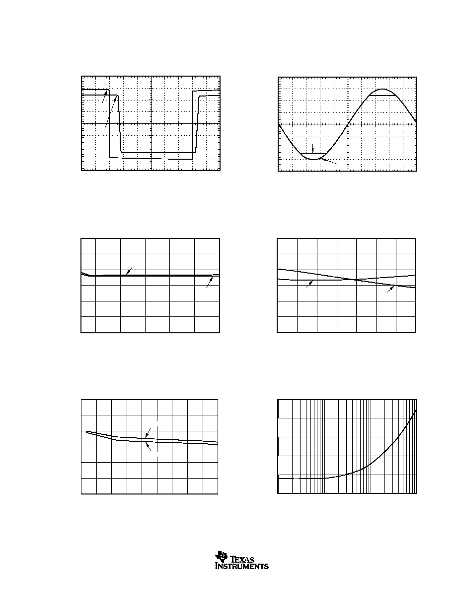
OVERLOAD RECOVERY
(G = +1)
1V/div
40
�
s/div
V
IN
V
OUT
NO PHASE INVERSION WITH INPUTS
LARGER THAN SUPPLY VOLTAGE
(G = +1, R
L
= 10
)
1V/div
1ms/div
V
IN
V
OUT
15
10
5
0
�5
�10
�15
CURRENT LIMIT ERROR vs TEMPERATURE
Temperature (
�
C)
Current Limit Error (%)
�55
�35
I
LIMIT
+
I
LIMIT
�
�15
5
25
45
65
85
15
10
5
0
�5
�10
�15
CURRENT LIMIT ERROR vs OUTPUT CURRENT
Output Current (A)
Current Limit Error (%)
0.2
0.4
0.6
0.8
1.0
1.2
1.4
1.6
1.8
2.0
I
LIMIT
+
I
LIMIT
�
50
40
30
20
10
0
OVERSHOOT vs LOAD CAPACITANCE
(G = +1, R
L
= 1k
)
Load Capacitance (pF)
Overshoot (%)
10
100
1k
10k
15
10
5
0
�5
�10
�15
CURRENT LIMIT ERROR vs SUPPLY VOLTAGE
Supply Voltage (V)
Current Limit Error (%)
I
LIMIT
+
I
LIMIT
�
2.7
3.0
3.5
4.0
4.5
5.0
5.5
OPA567
SBOS287A
12
www.ti.com
TYPICAL CHARACTERISTICS
(Cont.)
At T
A
= +25
�
C, V
S
= +5V, unless otherwise noted.
CLOSED-LOOP OUTPUT IMPEDANCE
vs FREQUENCY
Frequency (Hz)
100k
1M
2M
10k
Output Impedance (
)
100
10
1
0.1
G = 1
OPA567
SBOS287A
13
www.ti.com
APPLICATIONS INFORMATION
BASIC CONFIGURATION
Figure 1 shows the OPA567 connected as a basic non-
inverting amplifier. However, the OPA567 can be used in
virtually any op amp configuration. A current limit setting
resistor (R
SET
, in Figure 1) is essential to the OPA567
operation, and cannot be omitted.
Power-supply terminals should be bypassed with low series
impedance capacitors. Using larger tantalum and smaller
ceramic type capacitors in parallel is recommended. Power-
supply wiring should have low series impedance.
POWER SUPPLIES
The OPA567 operates with excellent performance from a
single (+2.7V to +5.5V) supply or from dual supplies. Power
supply voltages do not need to be equal as long as the total
voltage remains below 5.5V. Parameters that vary signifi-
cantly with operating voltage are shown in the
Typical
Characteristics section.
ADJUSTABLE CURRENT LIMIT AND CURRENT
LIMIT FLAG PIN
The OPA567 provides over-current protection to the load
through its accurate, user-adjustable current limit (pin 6). The
current limit value, I
LIMIT
, can be set from 0.2A to 2.2A by
controlling the current to the I
SET
pin. The current limit, I
LIMIT
,
will be 9800 � I
SET
, where I
SET
is the current through the I
SET
pin. Setting the current limit requires no special power
resistors. The output current does not flow through this pin.
Setting the current limit
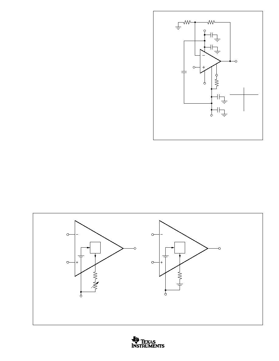
As illustrated in Figure 2, the simplest method of setting the
current limit is to connect a resistor or potentiometer between
FIGURE 1. Basic Connections.
FIGURE 2. Setting the Current Limit--Resistor Method.
the I
SET
pin and V�, the negative supply, according to the
formula:
I
LIMIT
= 9800 � (1.18V/R
SET
)
Alternatively, the output current limit can be set by applying
a voltage source in series with a resistance using the equa-
tion:
I
LIMIT
= 9800 � [(1.18V � V
ADJUST
)/R
SET
]
The voltage source must be referenced to V�.
V
IN
R
1
R
2
47
�
F
Enable
(2)
47
�
F
0.1
�
F
I
SET
47
�
F
1, 12
2, 3
8
9
11
6
4, 5
0.1
�
F
R
SET
(
)
I
LIMIT
(A)
23.2k
11.5k
7.68k
5.76k
0.5
1.0
1.5
2.0
R
SET
(1)
V+
NOTES: (1) R
SET
sets the current
limit value from 0.2A to 2.2A.
R
SET
can be a potentiometer to
easily adjust current limit and
calibrate out errors at the current
limit node. (2) Enable--pull Low
to disable output.
V
O
V�
OPA567
R
SET
V
ADJUST
(1)
(b) Resistor/Voltage Source Method
NOTE: (1) This voltage source must be able to
sink the current from the I
SET
pin, which is I
LIMIT
/9800.
1.18V
V�
I
LIMIT
= 9800 (1.18V � V
ADJUST
)
R
SET
I
SET
I
SET
8
9
6
2, 3
2, 3
4, 5
8
9
6
4, 5
R
POT
(a) Resistor or Potentiometer Method
Putting a set resistor in series with the potentiometer
will prevent potential short-circuit on pin.
1.18V
V�
I
LIMIT
= 9800 (1.18V/R
SET
)
OPA567
SBOS287A
14
www.ti.com
Current Limit Accuracy
Internally separate circuits monitor the positive and negative
current limits. Each circuit output is compared to a single
internal reference that is set by the user with an external
resistor or a resistor/voltage source combination. The OPA567
employs a patented circuit technique to achieve an accurate
and stable current limit throughout the full output range. The
initial accuracy of the current limit is typically within 3%;
however, because of internal matching limitations, the error
can be as much as 15%. The variation of the current limit with
factors such as output current level, output voltage, and
temperature is shown in the
Typical Characteristics section.
When the accuracy of one current limit (sourcing or sinking)
is more important than the other, it is possible to set its
accuracy to better than 1% by adjusting the external resistor
or the applied voltage. The accuracy of the other current limit
will still be affected by internal matching.
Current Limit Flag Pin
The OPA567 features an I
FLAG
pin (pin 7) that can be
monitored to determine when the part is in current limit. The
output signal of the I
FLAG
pin is compatible to standard logic
in single-supply applications. The output signal is a CMOS
logic gate that switches from V+ to V� to indicate that the
amplifier is in current limit. The I
FLAG
pin can source and sink
up to 25
�
A. Additional parasitic capacitance between pins 6
and 7 can cause instability at the edge of the current limit.
Avoid routing these traces in parallel close to each other.
Quiescent Current Dependence on the
Current Limit Setting
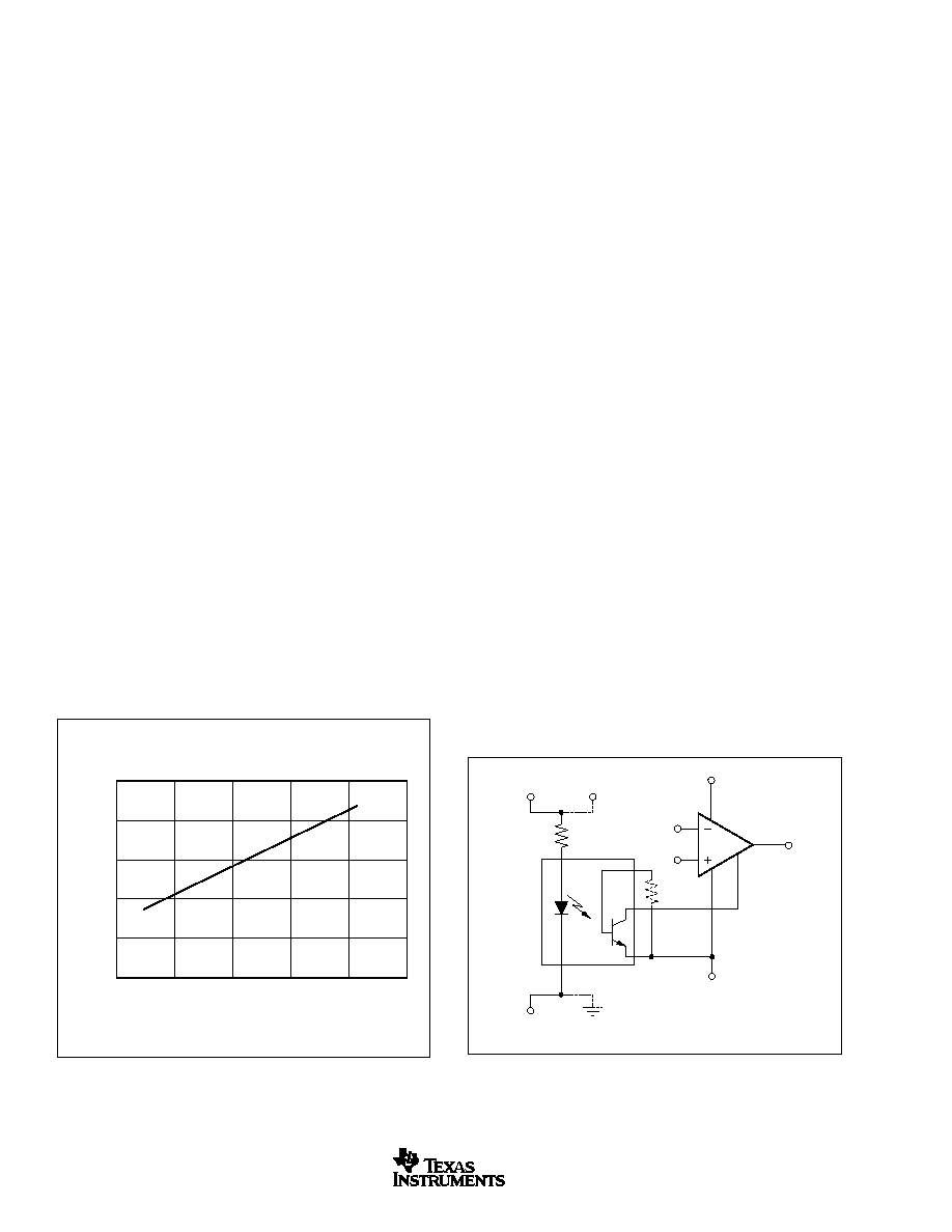
The OPA567 is a low-power amplifier, with a typical 3.4mA
quiescent current (with the current limit configured for 200mA).
The quiescent current varies with the current limit setting--
it increases 0.5mA for each additional 200mA increase in
the current limit, as shown in Figure 3.
FIGURE 3. Quiescent Current vs Current Limit Setting.
ENABLE PIN--OUTPUT DISABLE
The Enable pin can disable the OPA567 within microsec-
onds. When disabled, the amplifier draws less than 10
�
A and
its output enters a high-impedance state that allows multi-
plexing. It is important to note that when the amplifier is
disabled, the Thermal Flag pin (T
FLAG
) circuitry continues to
operate. This feature allows use of the T
FLAG
pin output to
implement thermal protection strategies. For more details,
please see the section on thermal protection.
The OPA567 Enable pin has an internal pull-up circuit, so it
does not have to be connected to the positive supply for
normal operation. To disable the amplifier, the Enable pin
must be connected to no more than (V�) + 0.8V. To enable
the amplifier, either allow the Enable pin to float or connect
it to at least (V�) + 2.5V.
The Enable pin is referenced to the negative supply (V�).
Therefore, shutdown operation is slightly different in single-
supply and dual-supply applications.
In single-supply operation, V� typically equals common
ground; thus, the enable/disable logic signal and the OPA567
Enable pin are referenced to the same potential. In this
configuration, the logic level and the OPA567 Enable pin can
simply be tied together. Disabling the OPA567 occurs for
voltage levels of less than 0.8V. The OPA567 is enabled at
logic levels greater than 2.5V.
In dual-supply operation, the logic level is referenced to a
logic ground. However, the OPA567 Enable pin is still refer-
enced to V�. To disable the OPA567, the voltage level of the
logic signal needs to be level-shifted. This level-shifting can
be done using an optocoupler, as shown in Figure 4.
Examples of output behavior during disabled and enabled
conditions with various load impedances are shown in the
typical characteristics section. Please note that this behavior
is a function of board layout, load impedances, and bypass
strategies. For sensitive loads, the use of a low-pass filter or
other protection strategy is recommended.
FIGURE 4. OPA567 Shutdown Configuration for Dual
Supplies.
10
8
6
4
2
0
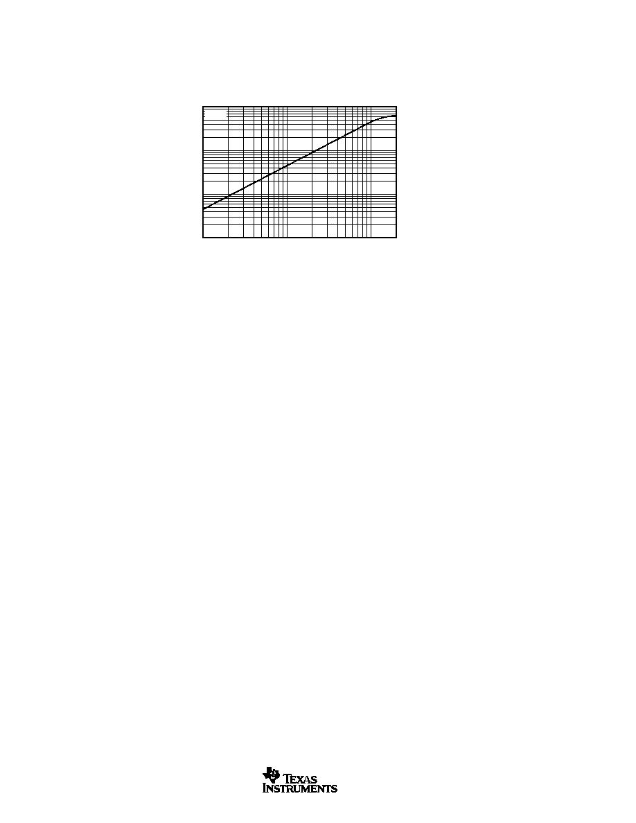
QUIESCENT CURRENT vs CURRENT LIMIT SETTING
Current Limit Setting (A)
Quiescent Current (mA)
0
0.5
1
1.5
2
2.5
Optocoupler
4N38
NOTE: (1) Optional--may be required
to limit leakage current of optocoupler
at high temperatures.
Enable
V+
V
O
8
9
11
2, 3
4, 5
1, 12
(a) +5V
(b) HCT or TTL In
HCT or
TTL In
(a)
(b)
OPA567
(1)
V�
OPA567
SBOS287A
15
www.ti.com
ENSURING MICROCONTROLLER COMPATIBILITY
Not all microcontrollers output the same logic state after
power-up or reset. 8051-type microcontrollers, for example,
output logic High levels on their ports while other models
power up with logic Low levels after reset.
In configuration (a) shown in Figure 4, the enable/disable
signal is applied on the cathode side of the photodiode within
the optocoupler. A logic High level causes the OPA567 to be
enabled, and a logic Low level disables the OPA567. In
configuration (b) of Figure 4, with the logic signal applied on
the anode side, a high level disables the OPA567 and a low
level enables the op amp.
RAIL-TO-RAIL OUTPUT RANGE
The OPA567 has a class AB output stage with common
source transistors that are used to achieve rail-to-rail output
swing. It was designed to be able to swing closer to the rail
than other existing linear amplifiers, even with high output
current levels. A quick way to estimate the output swing with
various output current requirements is by using the equation:
V
SWING
[typical] = 0.1 � I
O
Plots of the Output Swing vs Output Current, Supply Voltage,
and Temperature are provided in the Typical Characteristics
section.
RAIL-TO-RAIL INPUT RANGE
The input common-mode voltage range of the OPA567
extends 100mV beyond the supply rails. This is achieved by
a complementary input stage with an N-channel input differ-
ential pair in parallel with a P-channel differential pair. The
N-channel input pair is active for input voltages close to the
positive rail while the P-channel input pair is active for input
voltages close to the negative rail. The transition point is
typically at (V+) � 1.3V, and there is a small transition region
around the switching point where both transistors are on. It
is important to note that the two input pairs can have offsets
of different signs and magnitudes. Therefore, as the transi-
tion point is crossed, the offset of the amplifier changes. This
offset shift accounts for the reduced common-mode rejection
ratio over the full input common-mode range.
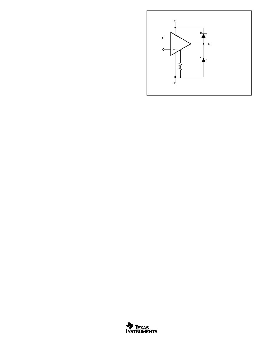
OUTPUT PROTECTION
Reactive and EMF-generating loads can return load current
to the amplifier, causing the output voltage to exceed the
power-supply voltage. This damaging condition can be
avoided with clamp diodes from the output terminal to the
power supplies, as shown in Figure 5. Schottky rectifier
diodes with a 3A or greater continuous rating are recom-
mended.
THERMAL FLAG PIN
The OPA567 has thermal sensing circuitry that provides a
warning signal when the die temperature exceeds safe limits.
Unless the T
FLAG
pin is connected to the Enable pin, when
this flag is triggered, the part continues to operate even
though the junction temperature exceeds 150
�
C. This default
operation allows maximum usable operation in very harsh
conditions but degrades reliability. The T
FLAG
pin can be used
to provide for orderly system shutdown before failure occurs.
It can be also used to evaluate the thermal environment to
determine need for and appropriate design of a shutdown
mechanism.
The thermal flag output signal is from a CMOS logic gate that
switches from V+ to V� to indicate that the amplifier is in
thermal limit. This flag output pin can source and sink up to
25
�
A. The T
FLAG
pin is HIGH during normal operation. Power
dissipated in the amplifier will cause the junction temperature
to rise. When the junction temperature exceeds 150
�
C, the
T
FLAG
pin will go Low, and remain Low until the amplifier has
cooled to 130
�
C. Despite this hysteresis, with a method of
orderly shutdown, the T
FLAG
pin can cycle on and off, de-
pending on load and signal conditions. This limits the dissi-
pation of the amplifier but may have an undesirable effect on
the load.
It is possible to connect the T
FLAG
pin directly to the Enable
pin for automatic shutdown protection. When both thermal
shutdown and the amplifier enable/disable functions are
desired, the externally generated control signal and the T
FLAG
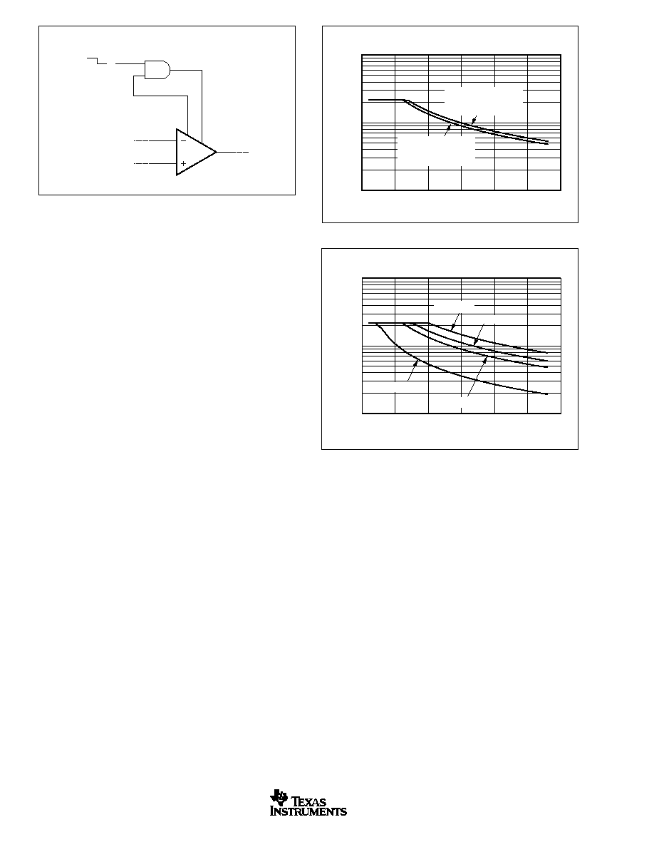
pin outputs should be combined with an AND gate; see
Figure 6. The temperature protection was designed to pro-
tect against overload conditions. It was not intended to
replace proper heatsinking. Continuously running the OPA567
in and out of thermal shutdown will degrade reliability.
FIGURE 5. Output Protection Diode.
OPA567
Output Protection Diode
Output Protection Diode
I
SET
R
SET
V
O
+V
1, 12
6
8
9
4, 5
�In
+In
2, 3
�V
OPA567
SBOS287A
16
www.ti.com
FIGURE 6. Enable/Shutdown Control Using T
FLAG
Pin and
External Control Signal.
Any tendency to activate the thermal protection circuit indi-
cates excessive power dissipation or an inadequate heat
sink. For reliable, long term, continuous operation, the junc-
tion temperature should be limited to 125
�
C maximum. To
estimate the margin of safety in a complete design (including
heat sink), increase the ambient temperature until the ther-
mal protection is triggered. Use worst-case loading and
signal conditions. For good, long-term reliability, thermal
protection should trigger more than 25
�
C above the maxi-
mum expected ambient conditions of your application. This
produces a junction temperature of 125
�
C at the maximum
expected ambient condition.
Fast transients of large output current swings (for example,
switching quickly from sourcing 2A to sinking 2A) may cause
a glitch on the T
FLAG
pin. When switching large currents is
expected, the use of extra bypass between the supplies or a
low-pass filter on the T
FLAG
pin is recommended.
POWER DISSIPATION AND
SAFE OPERATING AREA
Power dissipation depends on power supply, signal, and load
conditions. It is dominated by the power dissipation of the
output transistors. For DC signals, power dissipation is equal
to the product of output current, I
OUT
and the output voltage
across the conducting output transistor (V
S
� V
OUT
). Dissipa-
tion with AC signals is lower. Application Bulletin SBOA022
explains how to calculate or measure power dissipation with
unusual signals and loads and can be found at the TI web
site (www.ti.com).
Output short-circuits are particularly demanding for the am-
plifier because the full supply voltage is seen across the
conducting transistor. It is very important to note that the
temperature protection will not shut the part down in over-
temperature conditions, unless the T
FLAG
pin is connected to
the Enable pin; see the section on Thermal Flag.
Figure 7 shows the safe operating area at room temperature
with various heatsinking efforts. Note that the safe output
current decreases as (V
S
� V
OUT
) increases. Figure 8 shows
the safe operating area at various temperatures with the
metal heatsink being soldered to a 2oz copper pad.
FIGURE 7. Safe Operating Area at Room Temperature.
FIGURE 8. Safe Operating Area at Various Ambient Tempera-
tures. Metal heat sink soldered to a 2oz copper pad.
The power that can be safely dissipated in the package is
related to the ambient temperature and the heatsink design.
The QFN package was specifically designed to provide
excellent power dissipation, but board layout greatly influ-
ences the heat dissipation of the package. Refer to
the QFN Package section for further details.
The OPA567 has a junction-to-ambient thermal resistance
(
JA
) value of 38
�
C/W when soldered to a 2oz copper plane.
This value can be further decreased by the addition of forced
air. See Figure 9 for the junction-to-ambient thermal resis-
tance of the QFN-12 package.
Junction temperature should be kept below 125
�
C for reliable
operation. The junction temperature can be calculated by:
T
J
= T
A
+ P
D
JA
where
JA
=
JC
+
CA
T
J
= Junction Temperature (
�
C)
T
A
= Ambient Temperature (
�
C)
P
D
= Power Dissipated (W)
JA
= Junction-to-Ambient Thermal Resistance
JC
= Junction-to-Case Thermal Resistance
CA
= Case-to-Air Thermal Resistance
Enable Pin
2, 3
11
8
9
T
FLAG
Pin
Disable
On
10
AND
OPA567
10
1
0.1
V
S
� V
OUT
(V)
SAFE OPERATING AREA
(T
A
= 25
�
C)
Output Current (A)
0
1
2
3
4
5
6
Thermal pad soldered
to 2 oz. copper pad,
without forced air.
Thermal pad soldered
to 2 oz. copper pad,
with 500lfm airflow.
10
1
0.1
V
S
� V
OUT
(V)
SAFE OPERATING AREA
Thermal Pad Soldered, Various T
A
Output Current (A)
0
1
2
3
4
5
6
T
A
= +85
�
C
T
A
= +25
�
C
T
A
= �40
�
C
T
A
= 0
�
C
OPA567
SBOS287A
17
www.ti.com
FIGURE 9. Junction-to-Ambient Thermal Resistance with
Various Heatsinking Efforts.
FIGURE 10. Maximum Power Dissipation vs Temperature.
FIGURE 11. Thermal Resistance vs Number of Thermal Vias.
FIGURE 12. Feedback Capacitor for Use with Higher Imped-
ance Networks.
The Maximum Power Dissipation vs Temperature for the
heatsinking methods referenced in Figure 9 is shown in
Figure 10.
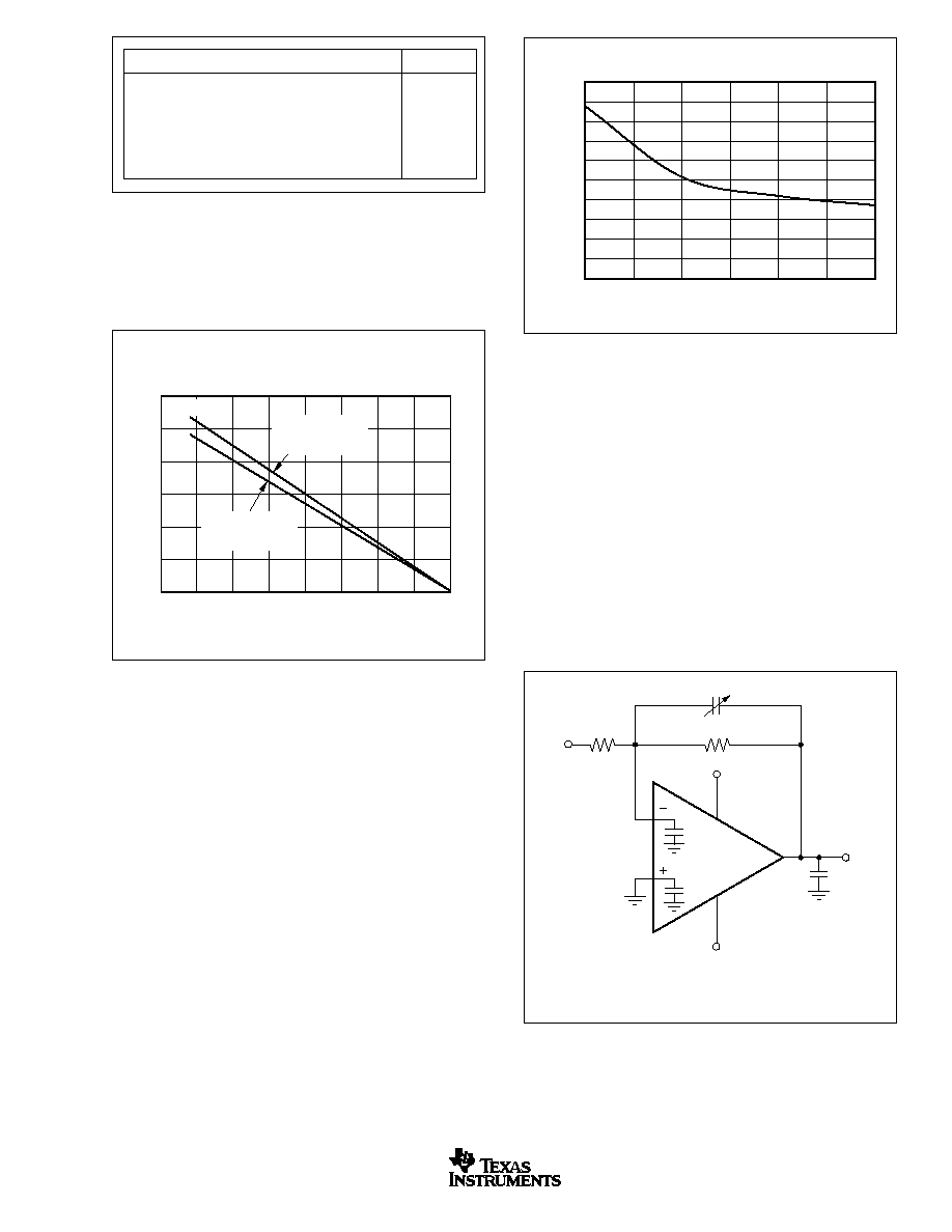
FEEDBACK CAPACITOR IMPROVES RESPONSE
For optimum settling time and stability with higher impedance
feedback networks (R
F
> 50k
), it may be necessary to add
a feedback capacitor across the feedback resistor, R
F
, as
shown in Figure 12. This capacitor compensates for the zero
created by the feedback network impedance and the input
capacitance of the OPA567 (and any parasitic layout capaci-
tance). The effect becomes more significant with higher
impedance networks.
The size of the capacitor needed is estimated using the
equation:
R
IN
� C
IN
= R
F
� C
F
where C
IN
is the sum of the input capacitance of the OPA567
plus the parasitic layout capacitance.
To appropriately determine required heatsink area, required
power dissipation should be calculated and the relationship
between power dissipation and thermal resistance should be
considered to minimize shutdown conditions and allow for
proper long-term operation (junction temperature of 125
�
C).
Once the heatsink area has been selected, worst-case load
conditions should be tested to ensure proper thermal protec-
tion.
For applications with limited board size, refer to Figure 11 for
the approximate thermal resistance relative to the number of
thermal vias. The QFN-12 package is well suited for continu-
ous power levels, as shown in Figure 10. Higher power levels
may be achieved in applications with a low on/off duty cycle.
OPA567
V+
V�
V
OUT
V
IN
R
IN
8
1, 12
2, 3
4, 5
9
R
IN
� C
IN
= R
F
�
C
F
R
F
C
L
C
IN
C
IN
C
F
Where C
IN
is equal to the OPA567 input
capacitance (approximately 9pF) plus any
parasitic layout capacitance.
HEATSINKING METHOD
JA
The part is soldered to a 2 oz copper pad under the
38
exposed pad.
Soldered to copper pad with forced airflow (150lfm).
36
Soldered to copper pad with forced airflow (250lfm).
35
Soldered to copper pad with forced airflow (500lfm).
34
6
5
4
3
2
1
0
Temperature (
�
C)
MAXIMUM POWER DISSIPATION IN PACKAGE
vs TEMPERATURE
Power Dissipated (W)
�75
�50
0
�25
25
50
75
100
125
Thermal pad soldered
to 2oz. copper pad,
with 500lfm airlow.
Thermal pad soldered
to 2oz. copper pad,
without forced air.
T
J
= 150
�
C
100
90
80
70
60
50
40
30
20
10
0
Thermal Resistance,
JA
(
�
C/W)
0
1
2
3
4
5
6
Number of Thermal Vias
THERMAL RESISTANCE
vs NUMBER OF THERMAL VIAS

OPA567
SBOS287A
18
www.ti.com
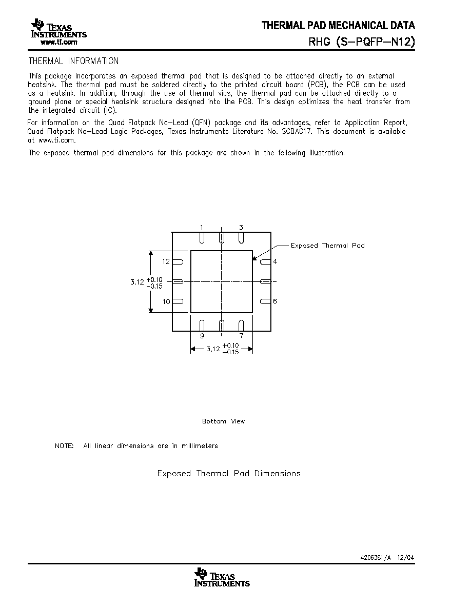
QFN THERMALLY ENHANCED PACKAGE
The OPA567 uses the QFN-12 package, a thermally-
enhanced package designed to eliminate the use of bulky
heat sinks and slugs traditionally used in thermal packages.
This package can be easily mounted using standard printed
circuit board (PCB) assembly techniques. See QFN/SON
PCB Attachment Application Note (SLUA271) located at
www.ti.com.
The thermal resistance junction-to-ambient (R
JA
) of the QFN
package depends on the PCB layout. Using thermal vias and
wide PCB traces improve thermal resistance. The thermal
pad must be soldered to the PCB. The thermal pad should
either be left floating or connected to V�.
LAYOUT GUIDELINES
The OPA567 is a power amplifier that requires proper layout
for best performance. An example layout is appended to the
end of this datasheet. Refinements to this layout may be
required based on assembly process requirements.
Keep power-supply leads as short as possible. This practice
will keep inductance low and resistive losses at a minimum.
A minimum of 18 gauge wire thickness is recommended for
power- supply leads. The wire length should be less than 8
inches.
Proper power-supply bypassing with low ESR capacitors is
essential to achieve good performance. A parallel combina-
tion of 100nF ceramic and 47
�
F tantalum bypass capacitors
will provide low impedance over a wide frequency range.
Bypass capacitors should be placed as close as practical to
the power-supply pins of the OPA567.
PCB traces conducting high currents, such as from output to
load or from the power-supply connector to the power-supply
pins of the OPA567 should be kept as wide and short as
possible. This practice will keep inductance low and resistive
losses to a minimum.
The nine holes in the landing pattern for the OPA567 are for
the thermal vias that connect the thermal pad of the OPA567
to the heatsink area on the PCB. All traces conducting high
currents are very wide for lowest inductance and minimal
resistive losses.
OPA567
SBOS287A
19
www.ti.com
FIGURE 15. Single Power Amplifier Driving Bidirectional Current through a TEC using Asymmetrical Bipolar Power Supplies.
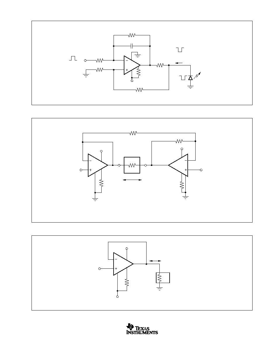
FIGURE 13. Grounded Anode LED Driver.
APPLICATION CIRCUITS
FIGURE 14. Bridge-Tied Load Driver.
Luxeon Star-0
High-Power LED
1, 12
8
9
4, 5
(1)
2, 3
6
R
SET
V
O
f
O
= 10kHz
V
IN
OPA567
R
1
49.9k
R
SHUNT
1
I
O
R
2
4.99k
4.99k
0.0033
�
F
R
3
49.9k
�5V
+1V
0V
0mA
�100mA
0V
�2.5V
Feedback for Constant Current,
1V Input per 100mA Output as Shown.
NOTE: (1) Bypass as recommended.
R
SET
V
SET
TEC
OPA567
1k
Heat/Cool
V
TEC
V
TEC
= 2 (V
IN
� V
SET
)
+
�
8
1, 12
4, 5
2, 3
I
SET
I
SET
4, 5
8
9
3
6
1, 12
2, 3
R
SET
NOTE: (1) Bypass as recommended.
5V
(1)
5V
9
1k
V
IN
OPA567
(1)
OPA567
8
1, 12
4, 5
6
�1.2V
2, 3
NOTE: Total Supply Must
be < 5.5V Cooling/Heating.
NOTE: (1) Bypass as recommended.
R
SET
I
SET
+3.3V
(1)
9
V
IN
TEC
I
L
OPA567
SBOS287A
20
www.ti.com

OPA567
SBOS287A
21
www.ti.com

PACKAGING INFORMATION
Orderable Device
Status
(1)
Package
Type
Package
Drawing
Pins Package
Qty
Eco Plan
(2)
Lead/Ball Finish
MSL Peak Temp
(3)
OPA567AIRHGR
ACTIVE
QFN
RHG
12
2500 Green (RoHS &
no Sb/Br)
CU NIPDAU
Level-2-260C-1 YEAR
OPA567AIRHGRG4
ACTIVE
QFN
RHG
12
2500 Green (RoHS &
no Sb/Br)
CU NIPDAU
Level-2-260C-1 YEAR
OPA567AIRHGT
ACTIVE
QFN
RHG
12
250
Green (RoHS &
no Sb/Br)
CU NIPDAU
Level-2-260C-1 YEAR
OPA567AIRHGTG4
ACTIVE
QFN
RHG
12
250
Green (RoHS &
no Sb/Br)
CU NIPDAU
Level-2-260C-1 YEAR
(1)
The marketing status values are defined as follows:
ACTIVE: Product device recommended for new designs.
LIFEBUY: TI has announced that the device will be discontinued, and a lifetime-buy period is in effect.
NRND: Not recommended for new designs. Device is in production to support existing customers, but TI does not recommend using this part in
a new design.
PREVIEW: Device has been announced but is not in production. Samples may or may not be available.
OBSOLETE: TI has discontinued the production of the device.
(2)
Eco
Plan
-
The
planned
eco-friendly
classification:
Pb-Free
(RoHS)
or
Green
(RoHS
&
no
Sb/Br)
-
please
check
http://www.ti.com/productcontent
for the latest availability information and additional product content details.
TBD: The Pb-Free/Green conversion plan has not been defined.
Pb-Free (RoHS): TI's terms "Lead-Free" or "Pb-Free" mean semiconductor products that are compatible with the current RoHS requirements
for all 6 substances, including the requirement that lead not exceed 0.1% by weight in homogeneous materials. Where designed to be soldered
at high temperatures, TI Pb-Free products are suitable for use in specified lead-free processes.
Green (RoHS & no Sb/Br): TI defines "Green" to mean Pb-Free (RoHS compatible), and free of Bromine (Br) and Antimony (Sb) based flame
retardants (Br or Sb do not exceed 0.1% by weight in homogeneous material)
(3)
MSL, Peak Temp. -- The Moisture Sensitivity Level rating according to the JEDEC industry standard classifications, and peak solder
temperature.
Important Information and Disclaimer:The information provided on this page represents TI's knowledge and belief as of the date that it is
provided. TI bases its knowledge and belief on information provided by third parties, and makes no representation or warranty as to the
accuracy of such information. Efforts are underway to better integrate information from third parties. TI has taken and continues to take
reasonable steps to provide representative and accurate information but may not have conducted destructive testing or chemical analysis on
incoming materials and chemicals. TI and TI suppliers consider certain information to be proprietary, and thus CAS numbers and other limited
information may not be available for release.
In no event shall TI's liability arising out of such information exceed the total purchase price of the TI part(s) at issue in this document sold by TI
to Customer on an annual basis.
PACKAGE OPTION ADDENDUM
www.ti.com
28-Oct-2005
Addendum-Page 1

IMPORTANT NOTICE
Texas Instruments Incorporated and its subsidiaries (TI) reserve the right to make corrections, modifications,
enhancements, improvements, and other changes to its products and services at any time and to discontinue
any product or service without notice. Customers should obtain the latest relevant information before placing
orders and should verify that such information is current and complete. All products are sold subject to TI's terms
and conditions of sale supplied at the time of order acknowledgment.
TI warrants performance of its hardware products to the specifications applicable at the time of sale in
accordance with TI's standard warranty. Testing and other quality control techniques are used to the extent TI
deems necessary to support this warranty. Except where mandated by government requirements, testing of all
parameters of each product is not necessarily performed.
TI assumes no liability for applications assistance or customer product design. Customers are responsible for
their products and applications using TI components. To minimize the risks associated with customer products
and applications, customers should provide adequate design and operating safeguards.
TI does not warrant or represent that any license, either express or implied, is granted under any TI patent right,
copyright, mask work right, or other TI intellectual property right relating to any combination, machine, or process
in which TI products or services are used. Information published by TI regarding third-party products or services
does not constitute a license from TI to use such products or services or a warranty or endorsement thereof.
Use of such information may require a license from a third party under the patents or other intellectual property
of the third party, or a license from TI under the patents or other intellectual property of TI.
Reproduction of information in TI data books or data sheets is permissible only if reproduction is without
alteration and is accompanied by all associated warranties, conditions, limitations, and notices. Reproduction
of this information with alteration is an unfair and deceptive business practice. TI is not responsible or liable for
such altered documentation.
Resale of TI products or services with statements different from or beyond the parameters stated by TI for that
product or service voids all express and any implied warranties for the associated TI product or service and
is an unfair and deceptive business practice. TI is not responsible or liable for any such statements.
Following are URLs where you can obtain information on other Texas Instruments products and application
solutions:
Products
Applications
Amplifiers
amplifier.ti.com
Audio
www.ti.com/audio
Data Converters
dataconverter.ti.com
Automotive
www.ti.com/automotive
DSP
dsp.ti.com
Broadband
www.ti.com/broadband
Interface
interface.ti.com
Digital Control
www.ti.com/digitalcontrol
Logic
logic.ti.com
Military
www.ti.com/military
Power Mgmt
power.ti.com
Optical Networking
www.ti.com/opticalnetwork
Microcontrollers
microcontroller.ti.com
Security
www.ti.com/security
Telephony
www.ti.com/telephony
Video & Imaging
www.ti.com/video
Wireless
www.ti.com/wireless
Mailing Address:
Texas Instruments
Post Office Box 655303 Dallas, Texas 75265
Copyright
2005, Texas Instruments Incorporated