©
1989 Burr-Brown Corporation
PDS-1026E
Printed in U.S.A. February, 1995
International Airport Industrial Park ∑ Mailing Address: PO Box 11400, Tucson, AZ 85734 ∑ Street Address: 6730 S. Tucson Blvd., Tucson, AZ 85706 ∑ Tel: (520) 746-1111 ∑ Twx: 910-952-1111
Internet: http://www.burr-brown.com/ ∑ FAXLine: (800) 548-6133 (US/Canada Only) ∑ Cable: BBRCORP ∑ Telex: 066-6491 ∑ FAX: (520) 889-1510 ∑ Immediate Product Info: (800) 548-6132
High Speed, Current-Feedback, High Voltage
OPERATIONAL AMPLIFIER
FEATURES
q
WIDE SUPPLY RANGE:
±
4.5 to
±
18V
q
BANDWIDTH: 100MHz, G = 1 to 10
q
SLEW RATE: 1000V/
µ
s
q
FAST SETTLING TIME: 50ns to 0.1%
q
HIGH OUTPUT CURRENT:
±
150mA peak
q
HIGH OUTPUT VOLTAGE:
±
12V
DESCRIPTION
The OPA603 is a high-speed current-feedback op amp
with guaranteed specifications at both
±
5V and
±
15V
power supplies. It can deliver full
±
10V signals into
150
loads with up to 1000V/
µ
s slew rate. This
allows it to drive terminated 75
cables. With 150mA
peak output current capability it is suitable for driving
load capacitance or long lines at high speed.
In contrast with conventional op amps, the current-
feedback approach provides nearly constant band-
width and settling time over a wide range of closed-
loop voltage gains.
The OPA603 is available in a plastic 8-pin DIP and
SO-16 surface-mount packages, specified over the
industrial temperature range.
APPLICATIONS
q
VIDEO AMPLIFIER
q
PULSE AMPLIFIER
q
SONAR, ULTRASOUND BUFFERS
q
ATE PIN DRIVERS
q
xDSL LINE DRIVER
q
FAST DATA ACQUISTION
q
WAVEFORM GENERATORS
≠V
S
4
+In
3
+V
S
7
V
O
6
≠In
2
Æ
OPA603
OPA603
OPA603
SBOS004

Æ
OPA603
2
OPA603AP, AU
PARAMETER
CONDITIONS
MIN
TYP
MAX
UNITS
INPUT OFFSET VOLTAGE
Initial
5
mV
vs Temperature
8
µ
V/
∞
C
vs Common-Mode Voltage
V
CM
=
±
10V
50
60
dB
vs Supply (tracking) Voltage
V
S
=
±
12V to
±
18V
80
85
dB
vs Supply (non-tracking)
(1)
|V
S
|
= 12V to 18V
55
60
dB
+INPUT BIAS CURRENT
Initial
5
µ
A
vs Temperature
30
nA/
∞
C
vs Common-Mode
V
CM
=
±
10V
200
500
nA/V
vs Supply (tracking)
V
S
=
±
12V to
±
18V
50
100
nA/V
vs Supply (non-tracking)
(1)
|V
S
|
= 12V to 18V
150
300
nA/V
≠INPUT BIAS CURRENT
Initial
25
µ
A
vs Temperature
300
nA/
∞
C
vs Common-Mode
V
CM
=
±
10V
200
600
nA/V
vs Supply (tracking)
V
S
=
±
12V to
±
18V
300
500
nA/V
vs Supply (non-tracking)
(1)
|V
S
|
= 12V to 18V
1500
2000
nA/V
INPUT IMPEDANCE
+Input
5 || 2
M
|| pF
≠Input
30 || 2
|| pF
OPEN LOOP CHARACTERISTICS
Transresistance
V
O
=
±
10V
300
440
k
Transcapacitance
1.8
pF
OUTPUT CHARACTERISTICS
Voltage
R
L
= 150
±
10
±
12
V
Peak Current
150
mA
Short-Circuit Current
(2)
V
O
= 0V
250
mA
Output Resistance, Open-Loop
70
FREQUENCY RESPONSE
G
= +2
Small-Signal Bandwidth
(3)
70
160
MHz
Gain Flatness,
±
0.5dB
35
75
MHz
Full-Power Bandwidth
V
O
= 20Vp-p
10
MHz
Differential Gain
f = 4.43MHz, V
O
= 1V
0.03
%
Differential Phase
f = 4.43MHz, V
O
= 1V
0.025
Degrees
TIME DOMAIN RESPONSE
G
= +2
Propagation Delay
10
ns
Rise and Fall Time
10
ns
Settling Time to 0.10%
10V Step
50
ns
Slew Rate
1000
V/
µ
s
DISTORTION
G
= +2, R
L
= 100
, f = 10MHz
2nd Harmonic Distortion
V
O
= 0.2Vp-p
≠60
≠65
dBc
3rd Harmonic Distortion
V
O
= 0.2Vp-p
≠70
≠90
dBc
POWER SUPPLY
Specified Operating Voltage
±
15
V
Operating Voltage Range
±
4.5
±
18
V
Current
±
21
±
25
mA
TEMPERATURE RANGE
Specification
≠25
+85
∞
C
Storage
≠40
+150
∞
C
THERMAL RESISTANCE,
JA
Soldered to Printed Circuit
90
∞
C/W
SPECIFICATIONS:
V
S
=
±
15V
ELECTRICAL
At T
A
= +25
∞
C, and R
L
= 150
,
unless otherwise noted.
NOTES: (1) One power supply fixed at 15V; the other supply varied from 12V to 18V. (2) Observe power derating curve. (3) See bandwidth versus gain curve,
Figure 5.
The information provided herein is believed to be reliable; however, BURR-BROWN assumes no responsibility for inaccuracies or omissions. BURR-BROWN assumes
no responsibility for the use of this information, and all use of such information shall be entirely at the user's own risk. Prices and specifications are subject to change
without notice. No patent rights or licenses to any of the circuits described herein are implied or granted to any third party. BURR-BROWN does not authorize or warrant
any BURR-BROWN product for use in life support devices and/or systems.

Æ
OPA603
3
OPA603AP, AU
PARAMETER
CONDITIONS
MIN
TYP
MAX
UNITS
INPUT OFFSET VOLTAGE
Initial
6
mV
vs Temperature
8
µ
V/
∞
C
vs Common-Mode
V
CM
=
±
3V
50
55
dB
vs Supply (tracking)
V
S
=
±
4V to
±
6V
75
80
dB
vs Supply (non-tracking)
(1)
|V
S
|
= 4V to 6V
55
60
dB
+INPUT BIAS CURRENT
Initial
5
µ
A
vs Temperature
30
nA/
∞
C
vs Common-Mode
V
CM
=
±
3V
350
600
nA/V
vs Supply (tracking)
V
S
=
±
4V to
±
6V
100
200
nA/V
vs Supply (non-tracking)
(1)
|V
S
|
= 4V to 6V
200
300
nA/V
≠INPUT BIAS CURRENT
Initial
25
µ
A
vs Temperature
300
nA/
∞
C
vs Common-Mode
V
CM
=
±
3V
300
600
nA/V
vs Supply (tracking)
V
S
=
±
4V to
±
6V
500
700
nA/V
vs Supply (non-tracking)
(1)
|V
S
|
= 4V to 6V
2500
3000
nA/V
INPUT IMPEDANCE
+Input
3.3 || 2
M
|| pF
≠Input
30 || 2
|| pF
OPEN LOOP CHARACTERISTICS
Transresistance
V
O
=
±
2V
225
330
k
Transcapacitance
2.4
pF
OUTPUT CHARACTERISTICS
Voltage
R
L
= 75
±
2
±
2.75
V
Peak Current
150
mA
Short-Circuit Current
(2)
V
O
= 0V
250
mA
Output Resistance, Open-Loop
80
FREQUENCY RESPONSE
G
= +2
Small-Signal Bandwidth
(3)
140
MHz
Gain Flatness,
±
0.5dB
65
MHz
Full-Power Bandwidth
20
MHz
Differential Gain
f = 4.43MHz, V
O
= 1V, R
L
= 150
0.03
%
Differential Phase
f = 4.43MHz, V
O
= 1V, R
L
= 150
0.025
Degrees
TIME DOMAIN RESPONSE
G
= +2, R
L
= 100
Propagation Delay
15
ns
Rise and Fall Time
20
ns
Settling Time to 0.10%
60
ns
Slew Rate
750
V/
µ
s
DISTORTION
G
= +2, R
L
= 100
, f = 10MHz
2nd Harmonic Distortion
V
O
= 0.2Vp-p
≠67
dBc
3rd Harmonic Distortion
V
O
= 0.2Vp-p
≠78
dBc
POWER SUPPLY
Specified Operating Voltage
±
5
V
Operating Voltage Range
±
4.5
±
18
V
Current
±
21
±
25
mA
TEMPERATURE RANGE
Specification
≠25
+85
∞
C
Storage
≠40
+150
∞
C
THERMAL RESISTANCE,
JUNCTION-AMBIENT
Soldered to Printed Circuit
90
∞
C/W
SPECIFICATIONS:
V
S
=
±
5V
ELECTRICAL
At T
A
= +25
∞
C, and R
L
= 75
,
unless otherwise noted.
NOTES: (1) One power supply fixed at 5V; the other supply varied from 4V to 6V. (2) Observe power derating curve. (3) See bandwidth versus gain curves,
Figure 5.
Æ
OPA603
4
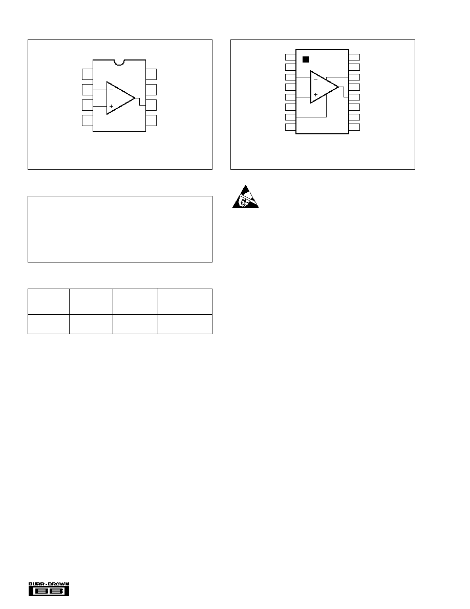
Top View
DIP
PIN CONFIGURATION
Top View
SO-16
1
2
3
4
5
6
7
8
NC
NC
≠In
NC
+In
NC
≠V
S
NC
NC: No Internal Connection.
Solder to ground plane for
improved heat dissipation.
16
15
14
13
12
11
10
9
NC
NC
+V
S
NC
V
O
NC
NC
NC
PIN CONFIGURATION
1
2
3
4
8
7
6
5
NC
≠In
+In
≠V
NC
+V
V
NC
S
S
NC: No Internal Connection.
Solder to ground plane for
improved heat dissipation.
O
PACKAGE/ORDERING INFORMATION
PACKAGE
SPECIFIED
DRAWING
TEMPERATURE
PRODUCT
PACKAGE
NUMBER
(1)
RANGE
OPA603AP
Plastic DIP
006
≠25
∞
C to +85
∞
C
OPA603AU
SO-16
211
≠25
∞
C to +85
∞
C
NOTE: (1) For detailed drawing and dimension table, please see end of data
sheet, or Appendix C of Burr-Brown IC Data Book.
ABSOLUTE MAXIMUM RATINGS
Supply Voltage ...................................................................................
±
18V
Input Voltage Range ............................................................................
±
V
S
Differential Input Voltage .....................................................................
±
6V
Power Dissipation ........................................................ See derating curve
Operating Temperature ................................................................. +100
∞
C
Storage Temperature ..................................................................... +150
∞
C
Junction Temperature .................................................................... +150
∞
C
Lead Temperature (soldering, 10s) ............................................... +300
∞
C
(soldering SO-16 package, 3s) ...................... +260
∞
C
ELECTROSTATIC
DISCHARGE SENSITIVITY
This integrated circuit can be damaged by ESD. Burr-Brown
recommends that all integrated circuits be handled with
appropriate precautions. Failure to observe proper handling and
installation procedures can cause damage.
ESD damage can range from subtle performance degradation to
complete device failure. Precision integrated circuits may be more
susceptible to damage because very small parametric changes
could cause the device not to meet its published specifications.
Æ
OPA603
5
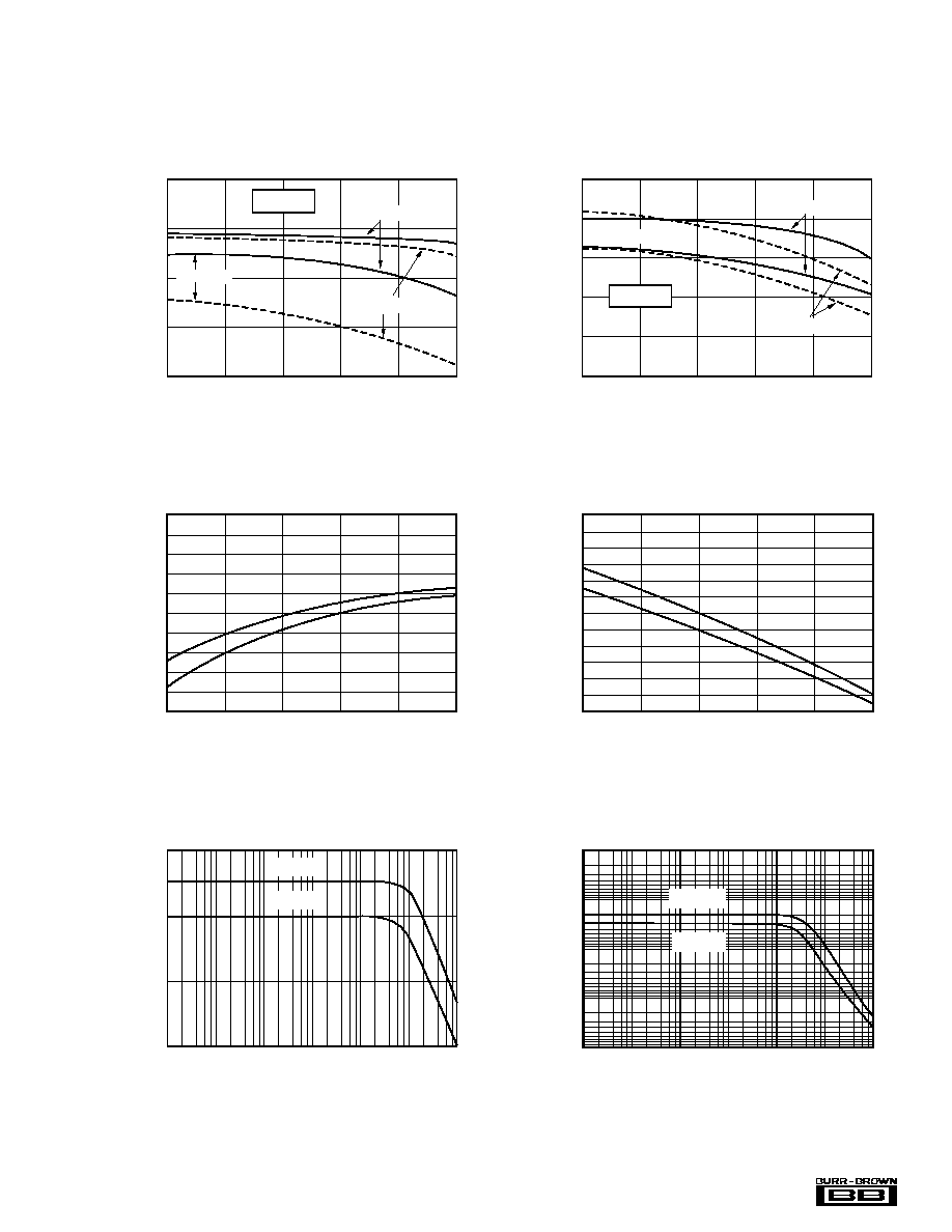
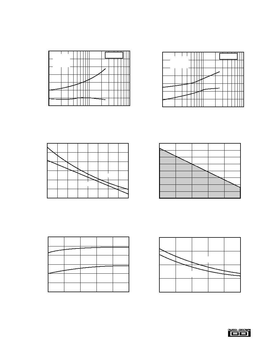
TYPICAL PERFORMANCE CURVES
At T
A
= +25
∞
C, unless otherwise noted.
OUTPUT SWING vs TEMPERATURE
≠25
0
+25
+50
+75
+100
Temperature (∞C)
Output Swing (V)
14
13
12
11
10
R = 150
L
R =
L
Positive Swing
Negative Swing
V = ±15V
S
OUTPUT SWING vs TEMPERATURE
≠25
0
+25
+50
+75
+100
Temperature (∞C)
Output Swing (V)
3.1
2.9
2.7
2.5
2.3
2.1
R = 75
L
R =
L
Positive Swing
Negative Swing
V = ±5V
S
NONINVERTING INPUT BIAS CURRENT
vs TEMPERATURE
≠25
0
+25
+50
+75
+100
Temperature (∞C)
+5
+4
+3
+2
+1
0
≠1
≠2
≠3
≠4
≠5
V = ±5V
S
V = ±15V
S
I + (µA)
B
INVERTING INPUT BIAS CURRENT
vs TEMPERATURE
≠25
0
+25
+50
+75
+100
Temperature (∞C)
+30
+20
+10
0
≠10
≠20
≠30
V = ±5V
S
V = ±15V
S
I ≠ (µA)
B
COMMON-MODE REJECTION vs FREQUENCY
65
55
45
35
10
100
1k
10k
100k
1M
10M
Frequency (Hz)
Common-Mode Rejection (dB)
V = ±15V
S
V = ±5V
S
I ≠ COMMON-MODE REJECTION RATIO
B
10
100
1k
10k
100k
1M
10M
Frequency (Hz)
10
10
10
10
10
≠8
≠7
≠6
≠5
≠4
I ≠ Common-Mode Rejection Ratio (A/V)
B
S
V = ±15V
S
V = ±5V
Æ
OPA603
6
TYPICAL PERFORMANCE CURVES
(CONT)
At T
A
= +25
∞
C, unless otherwise noted.
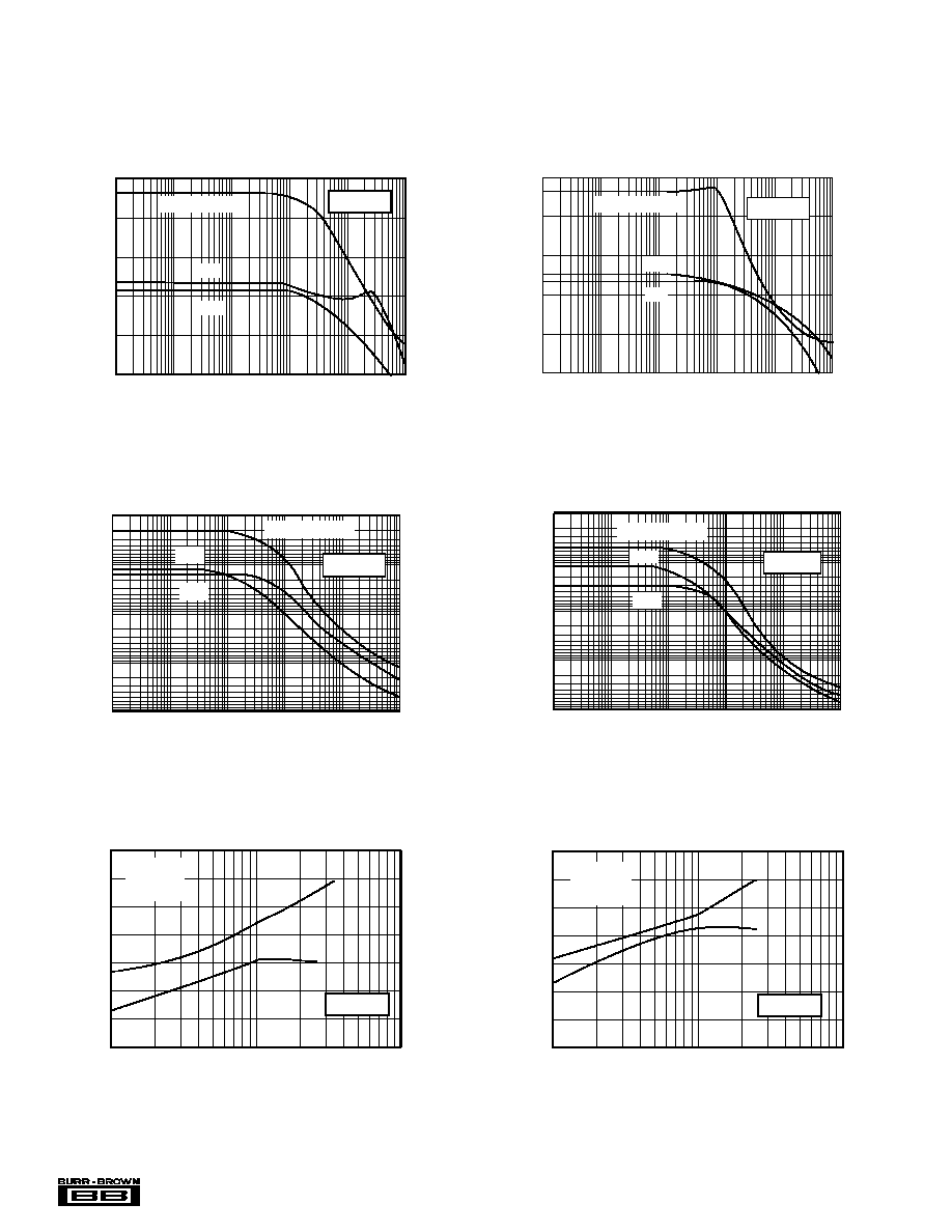
I ≠ PSRR vs FREQUENCY
B
10
100
1k
10k
100k
1M
Frequency (Hz)
10
10
10
10
10
≠7
≠6
≠5
≠4
≠3
I ≠ Power Supply Rejection Ratio (A/V)
B
V = ±15V
S
+V
S
Tracking Supplies
≠V
S
LARGE-SIGNAL
HARMONIC DISTORTION vs FREQUENCY
1
Frequency (MHz)
≠30
≠40
≠50
≠60
≠70
≠80
≠90
≠100
Harmonic Distortion (dBc)
10
100
G = +2
V = 2Vp-p
R = 100
O
L
2f
3f
V = ±15V
S
10
100
1k
10k
100k
1M
Frequency (Hz)
10
10
10
10
10
≠7
≠6
≠5
≠4
≠3
I ≠ Power Supply Rejection Ratio (A/V)
B
V = ±5V
S
+V
S
Tracking Supplies
≠V
S
I ≠ PSRR vs FREQUENCY
B
LARGE-SIGNAL
HARMONIC DISTORTION vs FREQUENCY
1
Frequency (MHz)
≠30
≠40
≠50
≠60
≠70
≠80
≠90
≠100
Harmonic Distortion (dBc)
10
100
G = +2V/V
V = 2Vp-p
R = 100
O
L
2f
3f
V = ±5V
S
POWER SUPPLY REJECTION vs FREQUENCY
10
Frequency (Hz)
90
80
70
60
50
40
100
1k
10k
100k
1M
Tracking Supplies
≠V
S
+V
S
Power Supply Rejection (dB)
V = ±15V
S
POWER SUPPLY REJECTION vs FREQUENCY
10
Frequency (Hz)
85
75
65
55
45
35
100
1k
10k
100k
1M
Tracking Supplies
Power Supply Rejection (dB)
≠V
S
+V
S
V = ±5V
S
Æ
OPA603
7
TYPICAL PERFORMANCE CURVES
(CONT)
At T
A
= +25
∞
C, unless otherwise noted.
SMALL-SIGNAL
HARMONIC DISTORTION vs FREQUENCY
1
Frequency (MHz)
≠30
≠40
≠50
≠60
≠70
≠80
≠90
≠100
Harmonic Distortion (dBc)
10
100
G = +2V/V
V = 0.5Vp-p
R = 100
O
L
2f
3f
V = ±15V
S
SMALL-SIGNAL
HARMONIC DISTORTION vs FREQUENCY
1
Frequency (MHz)
≠30
≠40
≠50
≠60
≠70
≠80
≠90
≠100
Harmonic Distortion (dBc)
10
100
G = +2V/V
V = 0.5Vp-p
R = 100
O
L
2f
3f
V = ±5V
S
OPEN-LOOP TRANSIMPEDANCE
vs TEMPERATURE
≠25
0
+25
+50
+75
+100
Temperature (∞C)
500
400
300
200
V = ±5V
S
V = ±15V
S
Open-Loop Transimpedance (k )
2-TONE, 3rd ORDER INTERMODULATION INTERCEPT
10
Frequency (MHz)
40
30
20
10
Intercept Point (+dBm)
20
30
40
50
V = ±15V
S
V = ±5V
S
OPEN-LOOP OUTPUT RESISTANCE vs TEMPERATURE
≠25
0
+25
+50
+75
+100
125
100
75
50
25
Open-Loop Output Resistance ( )
Temperature (∞C)
V = ±15V
S
V = ±5V
S
MAXIMUM POWER DISSIPATION vs TEMPERATURE
≠25
0
+25
+50
+75
+100
Temperature (∞C)
Power Dissipation (W)
2.0
1.5
1.0
0.5
Safe
Æ
OPA603
8
INPUT NOISE vs FREQUENCY
1
Frequency (Hz)
10
10
10
1
10
100
1k
10k
100k
Noise Voltage (nV/ Hz)
Noise Current (pA/ Hz)
10
10
10
1
Inverting Current
Noninverting Current
Voltage
3
2
3
2
V = ±15V
S
INPUT NOISE vs FREQUENCY
1
Frequency (Hz)
10
10
10
1
10
100
1k
10k
100k
Noise Voltage (nV/ Hz)
Noise Current (pA/ Hz)
10
10
10
1
Inverting Current
Noninverting Current
3
2
3
2
Voltage
V = ±5V
S
100
OPEN-LOOP PHASE vs FREQUENCY
Frequency (Hz)
0
≠45
≠90
≠135
≠180
Phase Shift (Degrees)
V = ±15V
S
V = ±5V
S
1k
10k
100k
1M
10M
1G
100M
100
OPEN-LOOP TRANSIMPEDANCE vs FREQUENCY
1G
Frequency (Hz)
10
10
10
10
10
Transimpedance ( )
6
5
4
3
2
1k
10k
100k
1M
10M
100M
V = ±15V
S
V = ±5V
S
LARGE-SIGNAL OUTPUT vs FREQUENCY
100
Frequency (Hz)
25
20
15
10
5
0
Output Voltage (Vp-p)
1k
10k
100k
1M
10M
100M
R = 150
L
S
V = ±15V
LARGE-SIGNAL OUTPUT vs FREQUENCY
100
Frequency (Hz)
5
4
3
2
1
0
Output Voltage (Vp-p)
1k
10k
100k
1M
10M
100M
R = 75
L
S
V = ±5V
TYPICAL PERFORMANCE CURVES
(CONT)
At T
A
= +25
∞
C, unless otherwise noted.
Noninverting Current
Voltage
Inverting Current
Æ
OPA603
9
TYPICAL PERFORMANCE CURVES
(CONT)
At T
A
= +25
∞
C, unless otherwise noted.
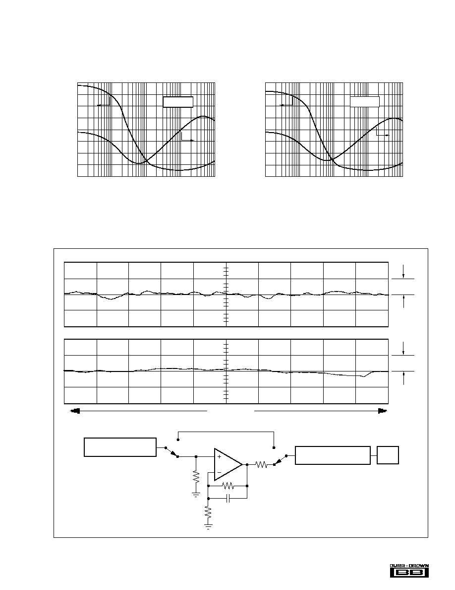
200 IRE Full Scale
FIGURE 1. Video Differential Gain/Phase Performance.
Measured with Rohde & Schwarz Differential Gain/Phase Meter.
499
5pF
75
75
499
V = ±5V
S
Rohde & Schwarz SPF2
Video Signal Generator
Rohde & Schwarz PVF
Differential Gain/Phase Meter
Scope
Plotter
OPEN-LOOP OUTPUT IMPEDANCE
80
60
40
20
0
Open- Loop Output Z Magnitude ( )
10k
100k
1M
10M
100M
90
45
0
≠45
≠90
Open-Loop Output Z Phase (∞)
Frequency (Hz)
V = ±15V
S
OPEN-LOOP OUTPUT IMPEDANCE
80
60
40
20
0
10k
100k
1M
10M
100M
90
45
0
≠45
≠90
Frequency (Hz)
V = ±5V
S
Open- Loop Output Z Magnitude ( )
Open-Loop Output Z Phase (∞)
0.05%
Gain
0.0625∞
Æ
OPA603
10
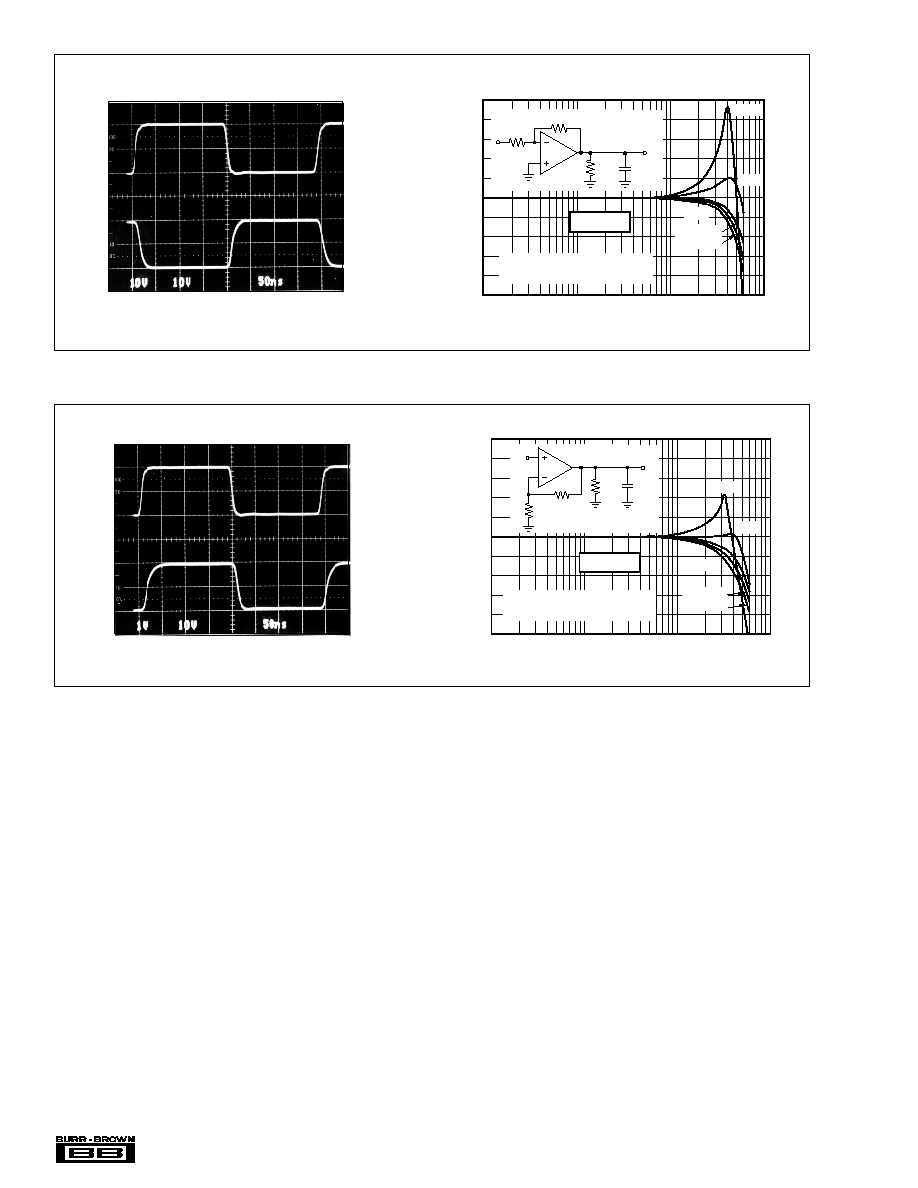
FIGURE 2. Dynamic Response, Inverting Unity-Gain.
SMALL-SIGNAL FREQUENCY RESPONSE
Frequency (Hz)
100k
1M
10M
100M
Gain (dB)
+6
+3
0
≠3
≠6
100pF
50pF
0pF
20pF
10pF
+
≠
V
IN
V
O
150
2.5k
V = ±15V
S
2.5k
NOTE: Feedback resistor value
selected for reduced peaking.
C
L
=
V
IN
V
O
150
C
L
2.5k
2.5k
LARGE SIGNAL PULSE RESPONSE
Input
Output
SMALL-SIGNAL FREQUENCY RESPONSE
Frequency (Hz)
100k
1M
10M
100M
Gain (dB)
+26
+23
+20
+17
+14
100pF
50pF
0pF
20pF
10pF
≠
+
V
IN
V
O
3570
402
150
NOTE: Feedback resistor value
selected for reduced peaking.
V = ±15V
FIGURE 3. Dynamic Response, Gain = +10.
C
L
=
V
IN
V
O
3570
402
150
C
L
S
LARGE SIGNAL PULSE RESPONSE
Output
Input
With control of the open-loop characteristics of the op amp,
dynamic behavior can be tailored to an application's require-
ments. Lower feedback resistance gives wider bandwidth,
more frequency-response peaking and more pulse response
overshoot. The higher open-loop gain resulting from lower
feedback network resistors also yields lower distortion.
Higher feedback network resistance gives an over-damped
response with little or no peaking and overshoot. This may
be beneficial when driving capacitive loads. Feedback net-
work impedance can also be varied to optimize dynamic
performance. To achieve wider bandwidth, use a feedback
resistor value somewhat lower than indicated in Figure 4.
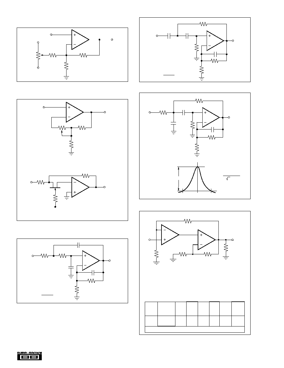
EXTENDING BANDWIDTH
For gains less than approximately 20, bandwidth can be
extended by adding a capacitor, C
F
, in parallel with a lower
value for R
F
. The optimum feedback resistor value in this
case is far lower than those shown in Figure 1. For
±
15V
operation, select R
F
with the following equation:
APPLICATIONS INFORMATION
For most circuit configurations, the OPA603 current-feed-
back op amp can be treated like a conventional op amp. As
with a conventional op amp, the feedback network con-
nected to the inverting input controls the closed-loop gain.
But with a current-feedback op amp, the impedance of the
feedback network also controls the open-loop gain and
frequency response.
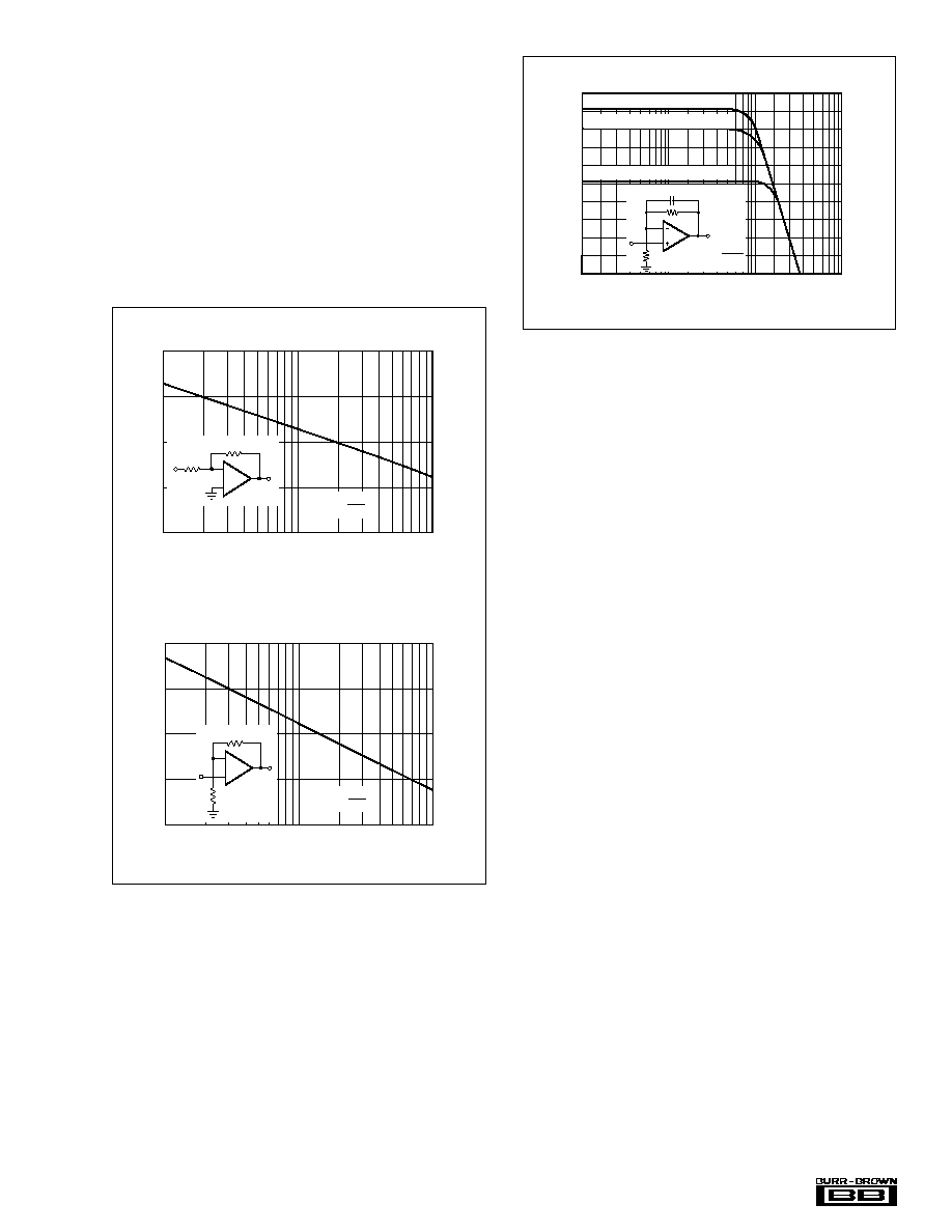
Feedback resistor values can be selected to provide a nearly
constant closed-loop bandwidth over a very wide range of
gain. This is in contrast to a conventional op amp where
circuit bandwidth is inversely proportional to the closed-
loop gain, sharply limiting bandwidth at high gain.
Figures 4a and 4b show appropriate feedback resistor values
versus closed-loop gain for maximum bandwidth with mini-
mal peaking. The dual vertical axes of these curves also
show the resulting bandwidth. Note that the bandwidth
remains nearly constant as gain is increased.
Æ
OPA603
11
R
F
(
) = 30 ∑ (30 ≠ G) for V
S
=
±
15V
For example, for a gain of 10, use R
F
= 600
. Optimum
values differ slightly for
±
5V operation:
R
F
(
) = 30 ∑ (23 ≠ G) for V
S
=
±
5V
C
F
will range from 1pF to 10pF depending on the selected
gain, load, and circuit layout. Adjust C
F
to optimize band-
width and minimize peaking. Figure 5 shows bandwidth
which can be acheived using this technique.
Typical values for this capacitor range from 1pF to 10pF
depending on closed-loop gain and load characteristics. Too
large a value of C
F
can cause instability.
FIGURE 5. Bandwidth Results with Added Capacitor C
F
.
VOLTAGE GAIN vs FREQUENCY
Voltage Gain (dB)
30
20
10
0
≠10
≠20
1M
10M
100M
1G
Frequency (Hz)
G = 2, R = 820 , C 3pF
F
F
G = 10, R = 560 , C 3pF
F
F
G = 20, R = 220 , C 8pF
F
F
R
I
R
F
C
F
R
F
R
I
G = 1 +
CIRCUIT LAYOUT
With any high-speed, wide-bandwidth circuitry, careful cir-
cuit layout will ensure best performance. Make short, direct
circuit interconnections and avoid stray wiring capacitance--
especially at the inverting input pin. A component-side
ground plane will help ensure low ground impedance. Do
not place the ground plane under or near the inputs and
feedback network.
Power supplies should be bypassed with good high-fre-
quency capacitors positioned close to the op amp pins. In
most cases, a 0.01
µ
F ceramic capacitor in parallel with a
2.2
µ
F solid tantalum capacitor at each power supply pin is
adequate. The OPA603 can deliver high load current--up to
150mA peak. Applications with low impedance or capaci-
tive loads demand large current transients from the power
supplies. It is the power supply bypass capacitors which
must supply these current transients. Larger bypass capaci-
tors such as 10
µ
F solid tantalum capacitors may improve
performance in these applications.
POWER DISSIPATION
High output current causes increased internal power dissipa-
tion in the OPA603. Copper leadframe construction maxi-
mizes heat dissipation compared to conventional plastic
packages. To achieve best heat dissipation, solder the device
directly to the circuit board and use wide circuit board
traces. Solder the unused pins, (1, 5 and 8) to a top-side
ground plane for improved power dissipation. Limit the load
and signal conditions depending on maximum ambient tem-
perature to assure operation within the power derating curve.
The OPA603 may be operated at reduced power supply
voltage to minimize power dissipation. Detailed specifica-
tions are provided for both
±
15V and
±
5V operation.
UNITY-GAIN OPERATION
As Figure 4b indicates, the OPA603 can be operated in unity
gain. A feedback resistor (approximately 2.8k
) sets the
appropriate open-loop characteristics and resistor R
I
is omit-
ted. Just as with gains greater than one, the value of the
feedback resistor (and capacitor if used) can be optimized
for the desired dynamic response and load characteristics.
Care should be exercised not to exceed the maximum differ-
ential input voltage rating of
±
6V. Large input voltage steps
which exceed the device's slew rate of 1000V/
µ
s can apply
excessive differential input voltage.
FIGURE 4. Feedback Resistor Selection Curves.
BANDWIDTH AND FEEDBACK RESISTOR
vs INVERTING GAIN
Voltage Gain (V/V)
(4a)
≠1
≠10
≠100
Closed-Loop Bandwidth (MHz)
60
52.5
45
37.5
30
Feedback Resistor (
)
3k
2.25k
1.5k
750
0
+
≠
R
F
R
I
G =
≠R
F
R
I
BANDWIDTH AND FEEDBACK RESISTOR
vs NONINVERTING GAIN
Voltage Gain (V/V)
(4b)
1
10
100
Closed-Loop Bandwidth (MHz)
60
52.5
45
37.5
30
Feedback Resistor (
)
4k
3k
2k
1k
0
+
≠
R
F
R
I
G = 1 +
R
F
R
I
Æ
OPA603
12
APPLICATIONS CIRCUITS
FIGURE 6. Offset Voltage Adjustment.
511
261
110
R
110
C
R
5pF
f =
1
2 2 RC
220
2R
100pF
C
22dB
1/2f
C
f
C
2f
C
V
IN
C
100pF
f = 10MHz
C
V
O
G = 70
OPA603
FIGURE 10. Bandpass Filter -- 10MHz.
FIGURE 9. High-Pass Filter -- 1MHz.
SLEW
GAIN
A
1
R
1
R
2
R
3
R
4
≠3dB
RATE
(V/V)
OP AMP
(
)
(k
)
(
)
(k
)
(MHz)
(V/
µ
s)
100
OPA627
50.5
(1)
4.99
20
1
15
700
1000
OPA637
49.9
4.99
12
1
11
500
This composite amplifier uses the OPA603 current-feedback op amp to
provide extended bandwidth and slew rate at high closed-loop gain.
The feedback loop is closed around the composite amp, preserving the
precision input characteristics of the OPA627/637. Use separate power
supply bypass capacitors for each op amp. See Application Bulletin
AB-007 for details.
NOTE: (1) Minimize capacitance at this node.
NOTE: (1) Closest 1/2% value.
FIGURE 11. Precision-Input Composite Amplifier.
A
1
R
1
R
3
R
4
V
I
R
2
V
O
(1)
OPA603
R 150
for ±10V
Out
L
FIGURE 7. Controlling Dynamic Performance.
FIGURE 8. Low-Pass Filter -- 10MHz.
V
IN
511
866
159
R
159
R
C
100pF
5pF
2-pole Butterworth LP
f = 10MHz
f =
1
2 RC
C
100pF
≠3dB
G = 1.6
≠3dB
V
O
OPA603
511
866
C
1590
C
R
5pF
2-pole Butterworth HP
f = 1MHz
f =
1
2 RC
1590
R
100pF
100pF
≠3dB
G = 1.6
≠3dB
V
IN
V
O
OPA603
V
O
R
F
R
G
10k
100k
V
IN
+15V
≠15V
OPA603
V
O
1k
G = 10
1k
110
V
O
1M
G = ≠10
1k
100
V
B
: 0V - Max Bandwidth
≠V - Reduced Bandwidth
MFE2000
(a)
(b)
Varying inverting input Z
changes dynamic response.
V
IN
V
IN
OPA603
OPA603

PACKAGING INFORMATION
ORDERABLE DEVICE
STATUS(1)
PACKAGE TYPE
PACKAGE DRAWING
PINS
PACKAGE QTY
OPA603AP
OBSOLETE
PDIP
P
8
OPA603AU
OBSOLETE
SOIC
DW
16
OPA603AU/1K
OBSOLETE
SOIC
DW
16
(1) The marketing status values are defined as follows:
ACTIVE: Product device recommended for new designs.
LIFEBUY: TI has announced that the device will be discontinued, and a lifetime-buy period is in effect.
NRND: Not recommended for new designs. Device is in production to support existing customers, but TI does not recommend using this part in
a new design.
PREVIEW: Device has been announced but is not in production. Samples may or may not be available.
OBSOLETE: TI has discontinued the production of the device.
PACKAGE OPTION ADDENDUM
www.ti.com
3-Oct-2003

IMPORTANT NOTICE
Texas Instruments Incorporated and its subsidiaries (TI) reserve the right to make corrections, modifications,
enhancements, improvements, and other changes to its products and services at any time and to discontinue
any product or service without notice. Customers should obtain the latest relevant information before placing
orders and should verify that such information is current and complete. All products are sold subject to TI's terms
and conditions of sale supplied at the time of order acknowledgment.
TI warrants performance of its hardware products to the specifications applicable at the time of sale in
accordance with TI's standard warranty. Testing and other quality control techniques are used to the extent TI
deems necessary to support this warranty. Except where mandated by government requirements, testing of all
parameters of each product is not necessarily performed.
TI assumes no liability for applications assistance or customer product design. Customers are responsible for
their products and applications using TI components. To minimize the risks associated with customer products
and applications, customers should provide adequate design and operating safeguards.
TI does not warrant or represent that any license, either express or implied, is granted under any TI patent right,
copyright, mask work right, or other TI intellectual property right relating to any combination, machine, or process
in which TI products or services are used. Information published by TI regarding third-party products or services
does not constitute a license from TI to use such products or services or a warranty or endorsement thereof.
Use of such information may require a license from a third party under the patents or other intellectual property
of the third party, or a license from TI under the patents or other intellectual property of TI.
Reproduction of information in TI data books or data sheets is permissible only if reproduction is without
alteration and is accompanied by all associated warranties, conditions, limitations, and notices. Reproduction
of this information with alteration is an unfair and deceptive business practice. TI is not responsible or liable for
such altered documentation.
Resale of TI products or services with statements different from or beyond the parameters stated by TI for that
product or service voids all express and any implied warranties for the associated TI product or service and
is an unfair and deceptive business practice. TI is not responsible or liable for any such statements.
Following are URLs where you can obtain information on other Texas Instruments products and application
solutions:
Products
Applications
Amplifiers
amplifier.ti.com
Audio
www.ti.com/audio
Data Converters
dataconverter.ti.com
Automotive
www.ti.com/automotive
DSP
dsp.ti.com
Broadband
www.ti.com/broadband
Interface
interface.ti.com
Digital Control
www.ti.com/digitalcontrol
Logic
logic.ti.com
Military
www.ti.com/military
Power Mgmt
power.ti.com
Optical Networking
www.ti.com/opticalnetwork
Microcontrollers
microcontroller.ti.com
Security
www.ti.com/security
Telephony
www.ti.com/telephony
Video & Imaging
www.ti.com/video
Wireless
www.ti.com/wireless
Mailing Address:
Texas Instruments
Post Office Box 655303 Dallas, Texas 75265
Copyright
2003, Texas Instruments Incorporated