 | –≠–ª–µ–∫—Ç—Ä–æ–Ω–Ω—ã–π –∫–æ–º–ø–æ–Ω–µ–Ω—Ç: OPA622AD | –°–∫–∞—á–∞—Ç—å:  PDF PDF  ZIP ZIP |
OPA622
FEATURES
q
LARGE SIGNAL BANDWIDTH:
150MHz (AP), 200MHz (AU)
(Voltage-Feedback)
q
HIGH OUTPUT CURRENT:
±
70mA
q
SLEW RATE: 1500V/
µ
s (AP), 1700V/
µ
s (AU)
q
DIFFERENTIAL GAIN: 0.15%
q
DIFFERENTIAL PHASE: 0.08
∞
q
EXCELLENT BANDWIDTH/SUPPLY
CURRENT RATIO: 200MHz/5mA
q
LOW INPUT BIAS CURRENT: ≠1.2
µ
A
APPLICATIONS
q
BROADCAST/HDTV EQUIPMENT
q
COMMUNICATIONS
q
PULSE/RF AMPLIFIERS
q
ACTIVE FILTER
q
HIGH SPEED ANALOG SIGNAL
PROCESSING
q
MULTIPLIER OUTPUT AMP
q
DIFFERENTIATOR FOR DIGITIZED
VIDEO SIGNALS
The feedback buffer stage provides 700MHz band-
width, a very high slew rate, and a very short signal
delay time. It is designed primarily for interstage
buffering and not for driving long cables. When com-
bined with the current-feedback amplifier section, the
OPA622 can be interconnected as a voltage-feedback
amplifier with two identical high-impedance inputs.
In this configuration, it features a low common-mode
gain, low input offset, and, due to the delay time of the
additional feedback buffer, a decrease in frequency
bandwidth compared with the current-feedback
configuration. Unlike "classical" operational amplifi-
ers, the OPA622 achieves a nearly constant bandwidth
over a wide gain and output voltage range. The
external setting of the open-loop gain with R
OG
avoids
a large compensation capacitor, improves the slew
rate, and allows a frequency response adaption to
various gains and load conditions.
International Airport Industrial Park ∑ Mailing Address: PO Box 11400 ∑ Tucson, AZ 85734 ∑ Street Address: 6730 S. Tucson Blvd. ∑ Tucson, AZ 85706
Tel: (520) 746-1111 ∑ Twx: 910-952-1111 ∑ Cable: BBRCORP ∑ Telex: 066-6491 ∑ FAX: (520) 889-1510 ∑ Immediate Product Info: (800) 548-6132
Wide-Bandwidth
OPERATIONAL AMPLIFIER
DESCRIPTION
The OPA622 is a monolithic amplifier component
designed for precision wide-bandwidth systems
including high-resolution video, RF and IF circuitry,
and communications equipment. It includes a mono-
lithic integrated current-feedback operational
amplifier block and a voltage buffer block, which,
when combined, form a voltage-feedback operational
amplifier.
When combined as a current-feedback amplifier, it
provides a 280MHz large-signal bandwidth at
±
2.5V
output level and a 1700V/
µ
s slew rate. The output
buffer stage can deliver
±
70mA output current. The
high output current capability allows the OPA622 to
drive two 50
or 75
lines with
±
3V output swing,
making it ideal along with the low differential
gain/phase errors for RF, IF, and video applications.
Æ
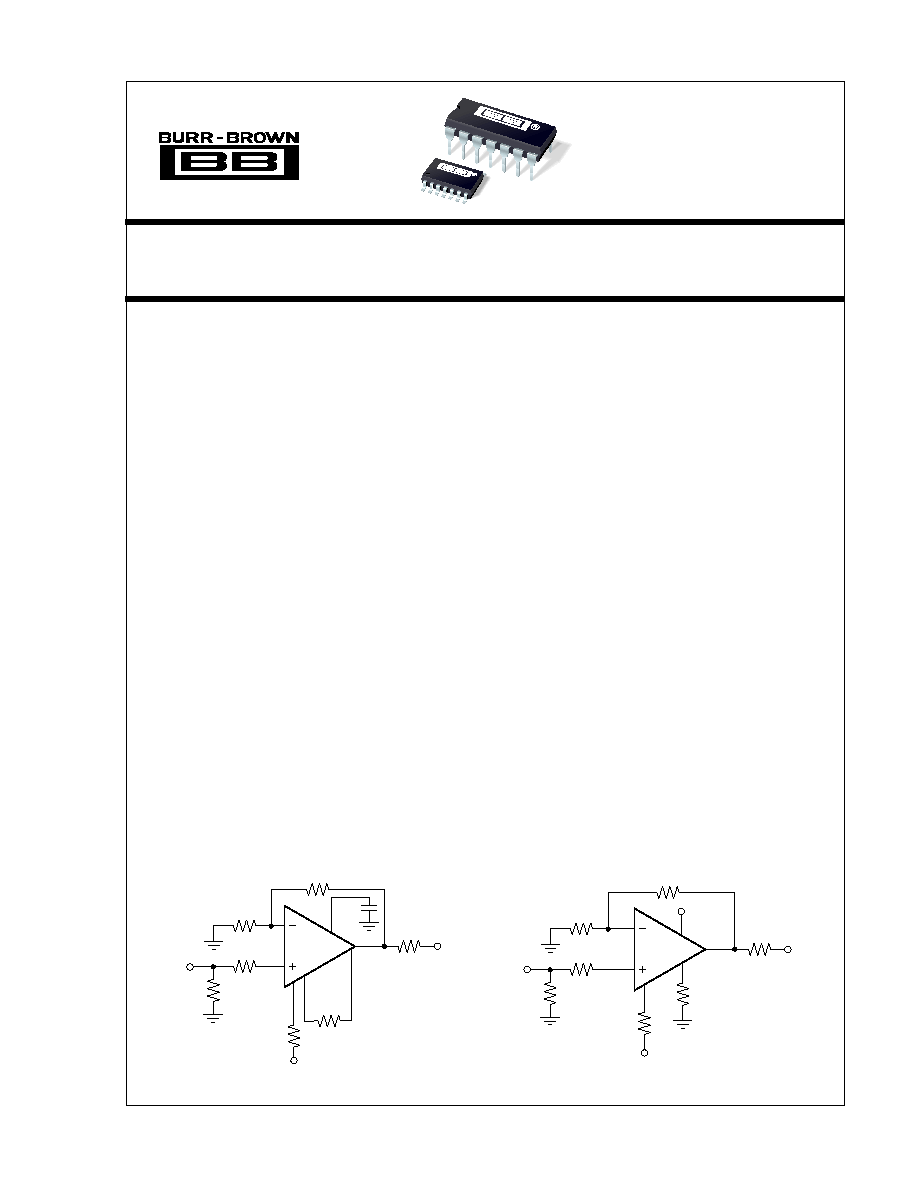
OPA622
OPA622
VOLTAGE-FEEDBACK
OPA622
VFA
3
4
+In
R
Q
R
1
R
IN
50
≠5V
V
IN
I
Q
Adjust
2
8
13
R
OG
9
50
R
2
V
OUT
10
≠In
BUF+
BUF≠
C
OTA
CURRENT-FEEDBACK
OPA622
CFA
4
+In
R
Q
R
IN
50
≠5V
V
IN
I
Q
Adjust
2
13
9
50
R
2
C
OTA
3
100
V
OUT
10
R
1
BUF+
© 1991 Burr-Brown Corporation
PDS-1131E
Printed in U.S.A. March, 1995
OPA622
2
Æ
SPECIFICATIONS
The information provided herein is believed to be reliable; however, BURR-BROWN assumes no responsibility for inaccuracies or omissions. BURR-BROWN assumes
no responsibility for the use of this information, and all use of such information shall be entirely at the user's own risk. Prices and specifications are subject to change
without notice. No patent rights or licenses to any of the circuits described herein are implied or granted to any third party. BURR-BROWN does not authorize or warrant
any BURR-BROWN product for use in life support devices and/or systems.
DC-SPECIFICATION
VOLTAGE-FEEDBACK AMPLIFIER (Figure 5)
At V
CC
=
±
5V, I
Q
=
±
5mA, G
CL
= +2V/V, R
LOAD
= 100
, R
SOURCE
= 50
,
R
Q
= 430
, R
OG
= 150
and T
A
= +25
∞
C, unless otherwise specified.
Power Supply Voltage .........................................................................
±
6V
Input Voltage
(1)
....................................................................
±
V
CC
to
±
0.7V
Operating Temperature ..................................................... ≠40
∞
C to +85
∞
C
Storage Temperature ...................................................... ≠40
∞
C to +125
∞
C
Junction Temperature .................................................................... +150
∞
C
Lead Temperature (soldering, 10s) ................................................ +300
∞
C
PACKAGE INFORMATION
PACKAGE DRAWING
MODEL
DESCRIPTION
NUMBER
(1)
OPA622AP
14-Pin Plastic DIP
010
OPA622AU
SO-14 Surface-Mount
235
NOTE:(1) For detailed drawing and dimension table, please see end of data
sheet, or Appendix D of Burr-Brown IC Data Book.
ABSOLUTE MAXIMUM RATINGS
NOTE: (1) Inputs are internally diode-clamped to
±
V
CC
.
ORDERING INFORMATION
MODEL
DESCRIPTION
TEMPERATURE RANGE
OPA622AP
14-Pin Plastic DIP
≠40
∞
C to +85
∞
C
OPA622AU
SO-14 Surface-Mount
≠40
∞
C to +85
∞
C
OPA622AP, AU
PARAMETER
CONDITIONS
MIN
TYP
MAX
UNITS
CLOSED-LOOP OUTPUT OFFSET VOLTAGE
Initial
1
±
15
mV
vs Temperature
210
µ
V/
∞
C
vs Supply (tracking)
V
CC
=
±
4.5V to
±
5.5V
≠46
≠50
dB
vs Supply (non-tracking)
V
CC
= +4.5V to +5.5V
≠43
dB
vs Supply (non-tracking)
V
CC
= ≠4.5V to ≠5.5V
≠51
dB
INPUT BIAS CURRENT
Initial
≠1.2
±
4
µ
A
vs Temperature
7
nA/
∞
C
vs Supply (tracking)
V
CC
=
±
4.5V to
±
5.5V
29
nA/V
vs Supply (non-tracking)
V
CC
= +4.5V to +5.5V
170
nA/V
vs Supply (non-tracking)
V
CC
= ≠4.5V to ≠5.5V
58
nA/V
OFFSET CURRENT
Input Offset Current
V
CM
= 0V
0.1
µ
A
INPUT IMPEDANCE
Differential Mode
2.4 || 1
M
|| pF
INPUT NOISE
Voltage Noise Density
f = 100kHz to 100MHz
11
nV/
MHz
Signal-to-Noise Ratio
S/N = 20 log 0.7/(V
N
∑
5MHz)
89
dB
INPUT VOLTAGE RANGE
Common-Mode Input Range
±
3.2
V
Common-Mode Rejection
V
I
= +2.5V, V
O
= 0V
78
dB
RATED OUTPUT
G
CL
= +1
Voltage Output
±
3
±
3.2
V
Closed-Loop Output Impedance
0.2
Current Output
70
mA
POWER SUPPLY
Rated Voltage
±
5
V
Derated Performance
±
4.5
±
5.5
V
Quiescent Current
R
Q
= 430
, I
O
= 0mA
±
4.4
±
5
±
5.6
mA
Quiescent Current (programmable)
Useful Range, I
O
= 0mA
3 to 8
mA
TEMPERATURE
Operating
Ambient Temperature
≠40
85
∞
C
Storage
Ambient Temperature
≠40
125
∞
C
OPA622
3
Æ
OPA622AP
OPA622AU
PARAMETER
CONDITIONS
TYP
TYP
UNITS
AC-SPECIFICATION
VOLTAGE-FEEDBACK AMPLIFIER (Figure 5)
At V
CC
=
±
5V, I
Q
=
±
5mA, G
CL
= +2V/V, R
LOAD
= 100
, R
SOURCE
= 50
,
R
Q
= 430
, R
OG
= 150
and T
A
= +25
∞
C, unless otherwise specified.
FREQUENCY DOMAIN
LARGE SIGNAL
V
O
= 2.8Vp-p, Gain = +1V/V
220
250
MHz
Closed-Loop Bandwidth (≠3dB)
V
O
= 2.8Vp-p, Gain = +2V/V
200
250
MHz
V
O
= 2.8Vp-p, Gain = +5V/V
170
230
MHz
V
O
= 2.8Vp-p, Gain = +10V/V
110
110
MHz
V
O
= 2.8Vp-p, Gain = ≠1V/V
150
250
MHz
V
O
= 2.8Vp-p, Gain = ≠2V/V
160
250
MHz
V
O
= 5.0Vp-p, Gain = +2V/V
150
200
MHz
SMALL SIGNAL BANDWIDTH
V
O
= 0.2Vp-p, Gain = +2V/V
150
170
MHz
GROUP DELAY TIME
1.4
1.4
ns
DIFFERENTIAL GAIN
f = 4.43MHz, R
LOAD
= 150
V
O
= 0.7V, Gain = +1V/V
0.12
0.12
%
V
O
= +1.4V, Gain = +2V/V
0.15
0.15
%
DIFFERENTIAL PHASE
f = 4.43MHz, R
LOAD
= 150
V
O
= 0.7V, Gain = +1V/V
0.06
0.06
Degrees
V
O
= +1.4V, Gain = +2V/V
0.08
0.08
Degrees
HARMONIC DISTORTION
Gain = +2V/V
Second Harmonic 2f
f = 10MHz, V
O
= 2.8Vp-p
≠57
≠57
dBc
Third Harmonic 3f
≠55
≠55
dBc
Second Harmonic 2f
f = 30MHz, V
O
= 2.8Vp-p
≠38
≠38
dBc
Third Harmonic 3f
≠43
≠43
dBc
Second Harmonic 2f
f = 50MHz, V
O
= 2.8Vp-p
≠33
≠33
dBc
Third Harmonic 3f
≠30
≠30
dBc
GAIN FLATNESS PEAKING
Gain = +2V/V
V
O
= 2.8Vp-p, DC to 30MHz
0.12
0.12
dB
V
O
= 2.8Vp-p, DC to 100MHz
0.3
0.3
dB
TIME DOMAIN
Rise Time
Gain = +2V/V, 10% to 90%
2.4
2.7
ns
V
O
= 5Vp-p, C
L
= 2pF
Fall Time
Gain = +2V/V, 10% to 90%
3.5
3.2
ns
V
O
= 5Vp-p, C
L
= 2pF
SLEW RATE
Gain = +2V/V, Rise Time = 2ns
V
O
= 6.2Vp-p
Positive
1500
1700
V/
µ
s
Negative
1300
1600
V
µ
s
SETTLING TIME
Gain = +2V/V, Rise Time = 2ns
V
O
= 2Vp-p, 0.1%
17
17
ns
OPA622
4
Æ
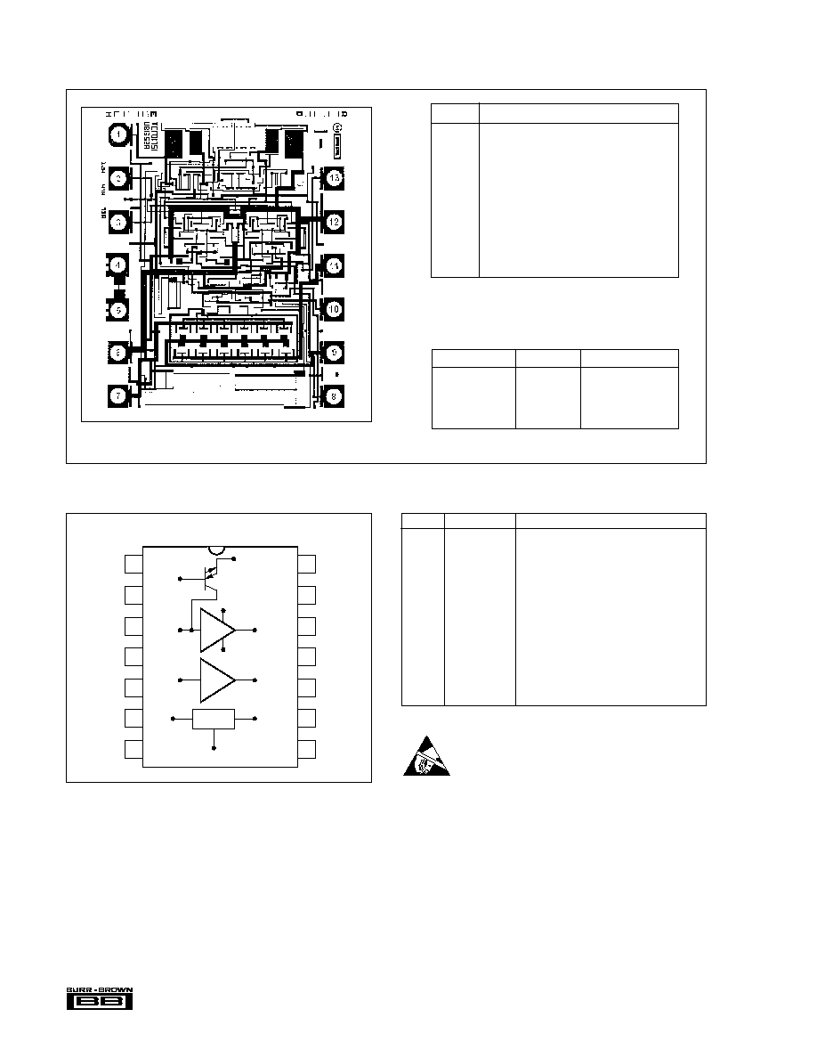
PAD
FUNCTION
1
Quiescent Current Adjustment
2
Inverting Analog Input
3
Non-Inverting Analog Input
4
NC
5
NC
6
≠5V Supply
7
≠5V Supply, Output
8
Inverting Buffer Output
9
Analog Output
10
Analog OTA Output
11
+5V Supply, Output
12
+5V Supply
13
Non-Inverting Buffer Output
Substrate Bias: Negative Supply
NC: No Connection
Wire Bonding: Gold wire bonding is recommended.
DICE INFORMATION
MECHANICAL INFORMATION
MILS (0.001")
MILLIMETERS
Die Size
57 x 69
±
5
1.44 x 1.76
±
0.13
Die Thickness
14
±
1
0.55
±
0.025
Min. Pad Size
4 x 4
0.10 x 0.10
Backing: Titanium
0.02+0.05,≠0.0
0.0005+0.0013, ≠0.0
Gold
0.30
±
0.05
0.0076
±
0.0013
OPA622AD DIE TOPOGRAPHY
PIN NO.
DESCRIPTION
FUNCTION
1
NC
No Connection
2
I
Q
Adjust
Quiescent Current Adjustment; typical 3-8mA
3
≠In
Inverting Analog Input
4
+In
Noninverting Analog Input
5
≠V
CC
Negative Supply Voltage; typical ≠5VDC
6
≠V
CC OUT
Negative Supply Voltage Output Buffer;
typical ≠5VDC
8
BUF≠
Analog Output Feedback Buffer
9
V
OUT
Analog Output
10
OTA
Analog Output OTA
11
+V
CC OUT
Positive Supply Voltage Output Buffer; typical
+5VDC
12
+V
CC
Positive Supply Voltage; typical +5VDC
13
BUF+
Analog Output/Input
14
NC
No Connection
PIN CONFIGURATION
FUNCTIONAL DESCRIPTION
NC
I
Q
Adjust
≠In
+In
≠V
CC
≠V
CC OUT
NC
NC
BUF+
+V
CC
+V
CC OUT
OTA
V
OUT
BUF≠
1
2
3
4
5
6
7
OPA622
14
13
12
11
10
9
8
FB
OTA
OB
13
4
10
3
5
12
2
Biasing
11
6
8
SO/DIP
9
Top View
ELECTROSTATIC
DISCHARGE SENSITIVITY
Electrostatic discharge can cause damage ranging from per-
formance degradation to complete device failure. Burr-
Brown Corporation recommends that all integrated circuits
be handled and stored using appropriate ESD protection
methods.
ESD damage can range from subtle performance degrada-
tion to complete device failure. Precision integrated circuits
may be more susceptible to damage because very small
parametric changes could cause the device not to meet
published specifications.
OPA622
5
Æ
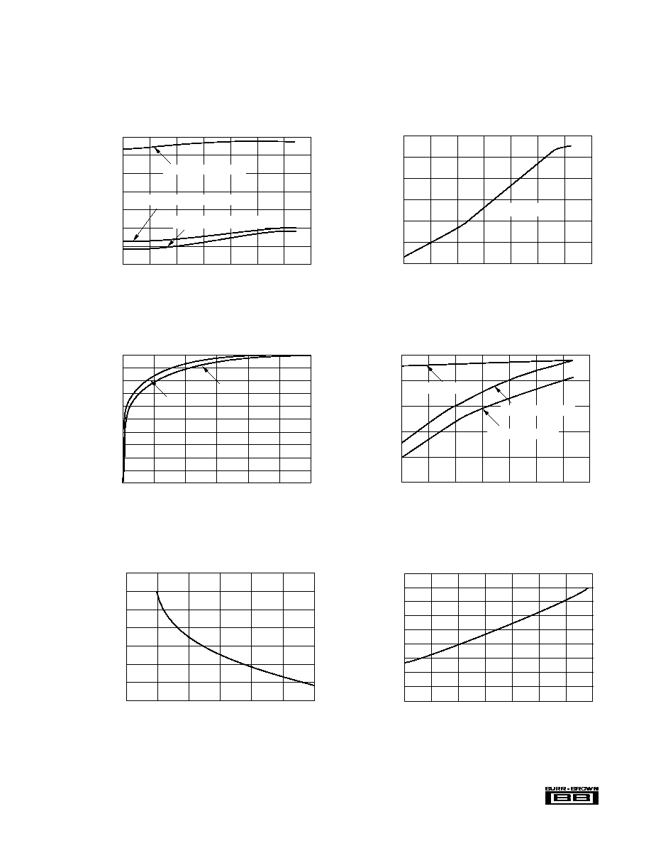
QUIESCENT CURRENT vs TEMPERATURE
9
8
7
6
5
4
3
2
1
0
≠40
≠20
0
20
40
60
80
100
Quiescent Current (mA)
Temperature (∞C)
QUIESCENT CURRENT vs R
Q
RESISTANCE
9
8
7
6
5
4
3
2
0
200
400
600
800
1000
1200
R
Q
(
)
Quiescent Current (mA)
INPUT STAGE OFFSET VOLTAGE vs TEMPERATURE
0.5
0
≠0.5
≠1
≠1.5
≠2
Temperature (∞C)
Offset Voltage Drift (mv)
≠40
≠20
0
20
40
60
80
100
Positive Input Voltage
Negative Input Voltage
Input Offset Voltage
INPUT OFFSET VOLTAGE vs TIME
100
90
80
70
60
50
40
30
20
10
0
V
OS
(% final value)
Time (minutes)
0
1
2
3
4
5
6
DIP
SO-14
INPUT BIAS CURRENT vs TEMPERATURE
0
≠0.2
≠0.4
≠0.6
≠0.8
≠1
≠1.2
≠1.4
Input Bias Current (µA)
Temperature (∞C)
≠40
≠20
0
20
40
60
80
100
Negative Input Bias Current
Input Bias Offset Current
Positive Input Bias Current
TYPICAL PERFORMANCE CURVES
VOLTAGE-FEEDBACK AMPLIFIER (Figure 5)
At V
CC
=
±
5V, I
Q
=
±
5mA, G
CL
= +2V/V, R
LOAD
= 100
, R
SOURCE
= 50
,
R
Q
= 430
, R
OG
= 150
and T
A
= +25
∞
C, unless otherwise specified.
CLOSED-LOOP OUTPUT OFFSET VOLTAGE
vs TEMPERATURE
15
10
5
0
≠5
≠10
≠15
Temperature (∞C)
Offset Voltage (mV)
≠40
≠20
0
20
40
60
80
100
G
CL
= +2V/V