DESCRIPTION
The OPA656 combines a very wideband, unity-gain stable,
voltage-feedback op amp with a FET-input stage to offer an
ultra high dynamic-range amplifier for ADC (Analog-to-Digital
Converter) buffering and transimpedance applications. Extremely
low DC errors give good precision in optical applications.
The high unity-gain stable bandwidth and JFET input allows
exceptional performance in high-speed, low-noise integrators.
The high input impedance and low bias current provided by
the FET input is supported by the ultra-low 7nV/
Hz input
voltage noise to achieve a very low integrated noise in
wideband photodiode transimpedance applications.
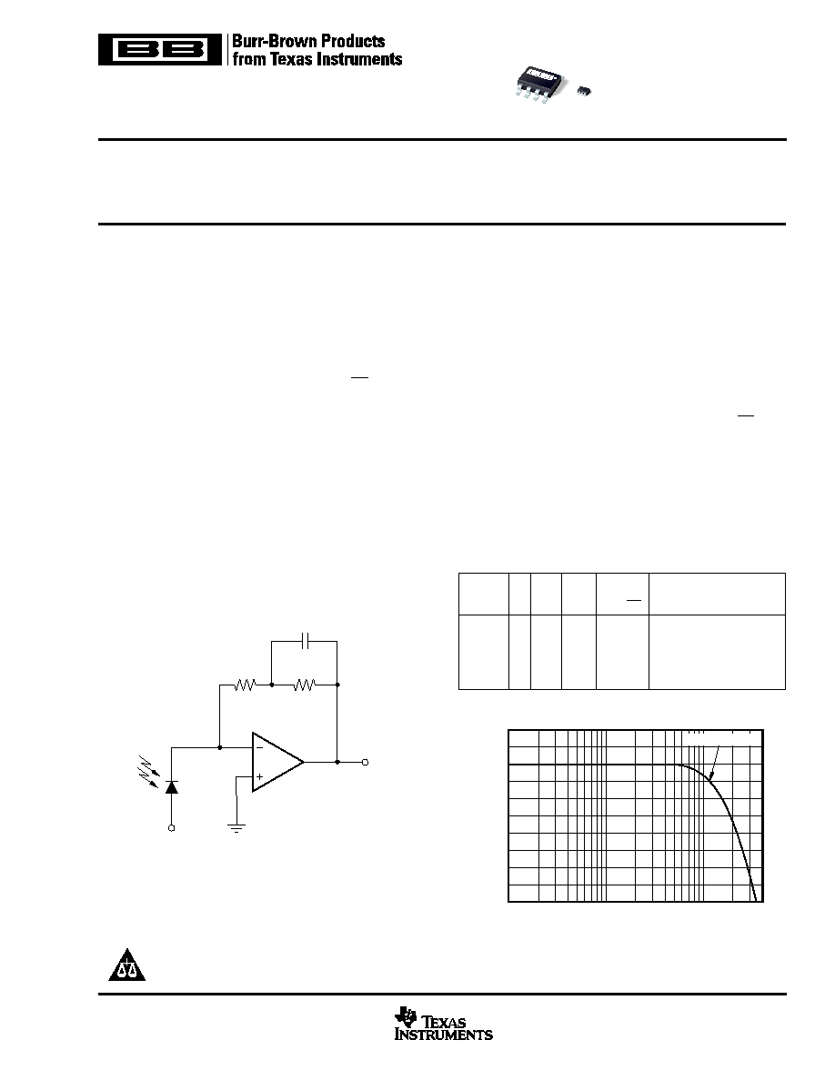
Broad transimpedance bandwidths are achievable given the
OPA656's high 230MHz gain bandwidth product. As shown
below, a ≠3dB bandwidth of 1MHz is provided even for a high
1M
transimpedance gain from a 47pF source capacitance.
FEATURES
q
500MHz UNITY-GAIN BANDWIDTH
q
LOW INPUT BIAS CURRENT: 2pA
q
LOW OFFSET AND DRIFT:
±
0.25mV,
±
2
µ
V/
∞
C
q
LOW DISTORTION: 74dB SFDR at 5MHz
q
HIGH OUTPUT CURRENT: 70mA
q
LOW INPUT VOLTAGE NOISE: 7nV/
Hz
Wideband, Unity-Gain Stable, FET-Input
OPERATIONAL AMPLIFIER
APPLICATIONS
q
WIDEBAND PHOTODIODE AMPLIFIERS
q
SAMPLE-AND-HOLD BUFFERS
q
CCD OUTPUT BUFFERS
q
ADC INPUT BUFFERS
q
WIDEBAND PRECISION AMPLIFIERS
q
TEST AND MEASUREMENT FRONT ENDS
Frequency
1M
TRANSIMPEDANCE BANDWIDTH
130
120
110
100
90
80
10kHz
100kHz
1MHz
5MHz
Transimpedance Gain (dB)
1MHz Bandwidth
OPA656
Wideband Photodiode Transimpedance Amplifier
(47pF)
≠V
b
499k
499k
V
O
1pF
OPA656
SBOS196B ≠ DECEMBER 2001 ≠ REVISED JUNE 2003
www.ti.com
Copyright © 2001-2003, Texas Instruments Incorporated
Please be aware that an important notice concerning availability, standard warranty, and use in critical applications of
Texas Instruments semiconductor products and disclaimers thereto appears at the end of this data sheet.
OPA656
SLEW VOLTAGE
V
S
BW
RATE
NOISE
DEVICE
(V) (MHz) (V/
µ
S)
(nV/
HZ)
AMPLIFIER DESCRIPTION
OPA355
+5
200
300
5.8
Unity-Gain Stable CMOS
OPA655
±
5
400
290
6
Unity-Gain Stable FET-Input
OPA657
±
5
1600
700
4.8
Gain of +7 Stable FET-Input
OPA627
±
15
16
55
4.5
Unity-Gain Stable FET-Input
THS4601
±
15
180
100
5.4
Unity-Gain Stable FET-Input
RELATED OPERATIONAL AMPLIFIER PRODUCTS
PRODUCTION DATA information is current as of publication date.
Products conform to specifications per the terms of Texas Instruments
standard warranty. Production processing does not necessarily include
testing of all parameters.

OPA656
2
SBOS196B
www.ti.com
SPECIFIED
PACKAGE
TEMPERATURE
PACKAGE
ORDERING
TRANSPORT
PRODUCT
PACKAGE-LEAD
DESIGNATOR
(1)
RANGE
MARKING
NUMBER
(2)
MEDIA, QUANTITY
OPA656U
SO-8 Surface Mount
D
≠40
∞
C to +85
∞
C
OPA656U
OPA656U
Rails, 100
"
"
"
"
"
OPA656U/2K5
Tape and Reel, 2500
OPA656UB
SO-8 Surface Mount
D
≠40
∞
C to +85
∞
C
OPA656UB
OPA656UB
Rails, 100
"
"
"
"
"
OPA656UB/2K5
Tape and Reel, 2500
OPA656N
SOT23-5
DBV
≠40
∞
C to +85
∞
C
B56
OPA656N/250
Tape and Reel, 250
"
"
"
"
"
OPA656N/3K
Tape and Reel, 3000
OPA656NB
SOT23-5
DBV
≠40
∞
C to +85
∞
C
B56
OPA656NB/250
Tape and Reel, 250
"
"
"
"
"
OPA656NB/3K
Tape and Reel, 3000
NOTE: (1) For the most current specifications and package information, refer to our web site at www.ti.com. (2) UB and NB are high grade, while U and N are
standard grade.
PACKAGE/ORDERING INFORMATION
ELECTROSTATIC
DISCHARGE SENSITIVITY
This integrated circuit can be damaged by ESD. Texas
Instruments recommends that all integrated circuits be handled
with appropriate precautions. Failure to observe proper han-
dling and installation procedures can cause damage.
ESD damage can range from subtle performance degrada-
tion to complete device failure. Precision integrated circuits
may be more susceptible to damage because very small
parametric changes could cause the device not to meet its
published specifications.
ABSOLUTE MAXIMUM RATINGS
(1)
Supply Voltage .................................................................................
±
6.5V
Internal Power Dissipation ........................... See Thermal Characteristics
Differential Input Voltage .....................................................................
±
V
S
Input Voltage Range ............................................................................
±
V
S
Storage Temperature Range ......................................... ≠40
∞
C to +125
∞
C
Lead Temperature ......................................................................... +260
∞
C
Junction Temperature (T
J
) ........................................................... +150
∞
C
ESD Rating (Human Body Model) .................................................. 2000V
(Machine Model) ............................................................ 200V
NOTE: (1) Stresses above these ratings may cause permanent damage.
Exposure to absolute maximum conditions for extended periods may degrade
device reliability. These are stress ratings only, and functional operation of the
device at these or any other conditions beyond those specified is not implied.
PIN CONFIGURATIONS
Top View
SO
Top View
SOT23
1
2
3
4
8
7
6
5
NC
+V
S
Output
NC
NC
Inverting Input
Noninverting Input
≠V
S
1
2
3
5
4
+V
S
Inverting Input
Output
≠V
S
Noninverting Input
B56
1
2
3
5
4
Pin Orientation/Package Marking

OPA656
3
SBOS196B
www.ti.com
ELECTRICAL CHARACTERISTICS: V
S
=
±
5V
R
F
= 250
, R
L
= 100
, and G = +2, unless otherwise noted. Figure 1 for AC performance.
OPA656U, N (Standard-Grade)
TYP
MIN/MAX OVER TEMPERATURE
0
∞
C to
≠40
∞
C to
MIN/
TEST
PARAMETER
CONDITIONS
+25
∞
C
+25
∞
C
(1)
70
∞
C
(2)
+85
∞
C
(2)
UNITS
MAX
LEVEL
(3)
AC PERFORMANCE (Figure 1)
Small-Signal Bandwidth
G = +1, V
O
= 200mVp-p, R
F
= 0
500
MHz
Typ
C
G = +2, V
O
= 200mVp-p
200
MHz
Typ
C
G = +5, V
O
= 200mVp-p
59
MHz
Typ
C
G = +10, V
O
= 200mVp-p
23
MHz
Typ
C
Gain-Bandwidth Product
G > +10
230
MHz
Typ
C
Bandwidth for 0.1dB flatness
G = +2, V
O
= 200mVp-p
30
MHz
Typ
C
Peaking at a Gain of +1
V
O
< 200mVp-p, R
F
= 0
1.5
dB
Typ
C
Large-Signal Bandwidth
G = +2, V
O
= 2Vp-p
75
MHz
Typ
C
Slew Rate
G = +2, 1V Step
290
V/
µ
s
Typ
C
Rise-and-Fall Time
0.2V Step
1.5
ns
Typ
C
Settling Time to 0.02%
G = +2, V
O
= 2V Step
21
ns
Typ
C
Harmonic Distortion
G = +2, f = 5MHz, V
O
= 2Vp-p
2nd-Harmonic
R
L
= 200
≠71
dBc
Typ
C
R
L
> 500
≠74
dBc
Typ
C
3rd-Harmonic
R
L
= 200
≠81
dBc
Typ
C
R
L
> 500
≠100
dBc
Typ
C
Input Voltage Noise
f > 100kHz
7
nV/
Hz
Typ
C
Input Current Noise
f > 100kHz
1.3
fA/
Hz
Typ
C
Differential Gain
G = +2, PAL, R
L
= 150
0.02
%
Typ
C
Differential Phase
G = +2, PAL, R
L
= 150
0.05
∞
Typ
C
DC PERFORMANCE
(4)
Open-Loop Voltage Gain (A
OL
)
V
O
= 0V, R
L
= 100
65
60
59
58
dB
Min
A
Input Offset Voltage
V
CM
= 0V
±
0.25
±
1.8
±
2.2
±
2.6
mV
Max
A
Average Offset Voltage Drift
V
CM
= 0V
±
2
±
12
±
12
±
12
µ
V/
∞
C
Max
A
Input Bias Current
V
CM
= 0V
±
2
±
20
±
1800
±
5000
pA
Max
A
Input Offset Current Drift
V
CM
= 0V
±
1
±
10
±
900
±
2500
pA
Max
B
INPUT
Most Positive Input Voltage
(5)
+2.5
+2.0
+1.9
+1.8
V
Min
A
Most Negative Input Voltage
(5)
≠4.0
≠3.5
≠3.4
≠3.3
V
Min
A
Common-Mode Rejection Ratio (CMRR)
V
CM
=
±
0.5V
86
80
78
76
dB
Min
A
Input Impedance
Differential
10
12
|| 0.7
|| pF
Typ
C
Common-Mode
10
12
|| 2.8
|| pF
Typ
C
OUTPUT
Voltage Output Swing
No Load
±
3.9
±
3.7
V
Typ
R
L
= 100
±
3.5
±
3.3
±
3.2
±
3.1
V
Min
A
Current Output, Sourcing
+70
56
54
50
mA
Min
A
Current Output, Sinking
≠70
≠56
≠54
≠50
mA
Min
A
Closed-Loop Output Impedance
G = +1, f = 0.1MHz
0.01
Typ
C
POWER SUPPLY
Specified Operating Voltage
±
5
V
Typ
C
Maximum Operating Voltage Range
±
6
±
6
±
6
V
Max
A
Maximum Quiescent Current
14
15.8
16
16.1
mA
Max
A
Minimum Quiescent Current
14
11.7
11.4
11.1
mA
Min
A
Power-Supply Rejection Ratio (+PSRR)
+V
S
= 4.50V to 5.50V
76
72
70
68
dB
Min
A
(≠PSRR)
≠V
S
= 4.50V to ≠5.50V
62
56
54
52
dB
Min
A
TEMPERATURE RANGE
Specified Operating Range: U, N Package
≠40 to 85
∞
C
Typ
Thermal Resistance,
JA
Junction-to-Ambient
U: SO-8
125
∞
C/W
Typ
N: SOT23-5
150
∞
C/W
Typ
NOTES: (1) Junction temperature = ambient for 25
∞
C min/max specifications.(2) Junction temperature = ambient at low temperature limit: junction temperature = ambient
+20
∞
C at high temperature limit for over temperature min/max specifications. (3) Test Levels: (A) 100% tested at 25
∞
C. Over temperature limits by characterization and
simulation. (B) Limits set by characterization and simulation. (C) Typical value only for information. (4) Current is considered positive out-of-node. V
CM
is the input
common-mode voltage. (5) Tested < 3dB below minimum specified CMRR at
±
CMIR limits.

OPA656
4
SBOS196B
www.ti.com
ELECTRICAL CHARACTERISTICS: V
S
=
±
5V:
High Grade DC Specifications
(1)
R
F
= 250
, R
L
= 100
, and G = +2, unless otherwise noted.
OPA656UB, NB (High-Grade)
TYP
MIN/MAX OVER TEMPERATURE
0
∞
C to
≠40
∞
C to
MIN/
TEST
PARAMETER
CONDITIONS
+25
∞
C
+25
∞
C
(2)
70
∞
C
(3)
+85
∞
C
(3)
UNITS
MAX
LEVEL
(4)
Input Offset Voltage
V
CM
= 0V
±
0.1
±
0.6
±
0.85
±
0.9
mV
Max
A
Input Offset Voltage Drift
V
CM
= 0V
±
2
±
6
±
6
±
6
µ
V/
∞
C
Max
A
Input Bias Current
V
CM
= 0V
±
1
±
5
±
450
±
1250
pA
Max
A
Input Offset Current
V
CM
= 0V
±
0.5
±
5
±
450
±
1250
pA
Max
A
Common-Mode Rejection Ratio (CMRR)
V
CM
=
±
0.5V
95
88
86
84
dB
Min
A
Power-Supply Rejection Ratio (+PSRR)
+V
S
= 4.5V to 5.5V
78
74
72
70
dB
Min
A
(≠PSRR)
≠V
S
= ≠4.5V to ≠5.5V
68
62
60
58
dB
Min
A
NOTES: (1) All other specifications are the same as the standard-grade. (2) Junction temperature = ambient for 25
∞
C min/max specifications.(3) Junction
temperature = ambient at low temperature limit: junction temperature = ambient +20
∞
C at high temperature limit for over temperature min/max specifications.
(4) Test Levels: (A) 100% tested at 25
∞
C. Over temperature limits by characterization and simulation.
OPA656
5
SBOS196B
www.ti.com
TYPICAL CHARACTERISTICS: V
S
=
±
5V
T
A
= +25
∞
C, G
= +2, R
F
= 250
, R
L
= 100
, unless otherwise noted.
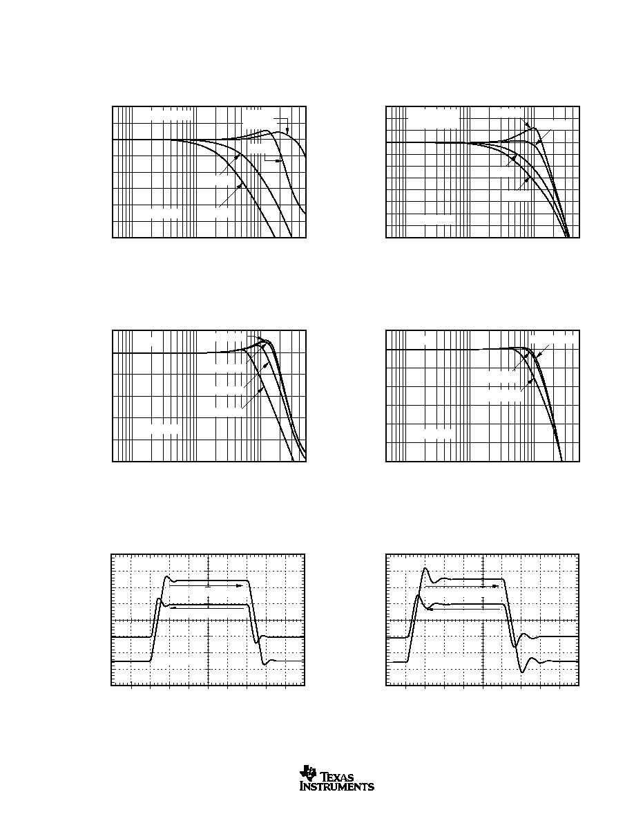
NONINVERTING SMALL-SIGNAL
FREQUENCY RESPONSE
10
0.5
1
500
100
Frequency (MHz)
Normalized Gain (dB)
6
3
0
≠3
≠6
≠9
≠12
≠15
≠18
See Figure 1
G = +2
G = +1
R
F
= 0
G = +5
G = +10
V
O
= 200mVp-p
INVERTING SMALL-SIGNAL
FREQUENCY RESPONSE
10
0.5
1
500
100
Frequency (MHz)
Normalized Gain (dB)
9
6
3
0
≠3
≠6
≠9
≠12
≠15
≠18
≠21
≠24
See Figure 2
G = ≠2
G = ≠1
G = ≠5
G = ≠10
V
O
= 200mVp-p
R
F
= 402
NONINVERTING LARGE-SIGNAL
FREQUENCY RESPONSE
10
0.5
1
500
100
Frequency (MHz)
Gain (dB)
9
6
3
0
≠3
≠6
≠9
See Figure 1
V
O
= 0.2Vp-p
V
O
= 0.5Vp-p
V
O
= 1Vp-p
V
O
= 2Vp-p
G = +2
INVERTING LARGE-SIGNAL
FREQUENCY RESPONSE
10
0.5
1
500
100
Frequency (MHz)
Gain (dB)
3
0
≠3
≠6
≠9
≠12
≠15
≠18
V
O
= 0.5Vp-p
V
O
= 1Vp-p
V
O
= 2Vp-p
See Figure 2
G = ≠1
NONINVERTING PULSE RESPONSE
Time (10ns/div)
Small-Signal Output V
oltage (200mV/div)
Large-Signal Output V
oltage (400mV/div)
0.8
0.6
0.4
0.2
0
≠0.2
≠0.4
≠0.6
≠0.8
1.6
1.2
0.8
0.4
0
≠0.4
≠0.8
≠1.2
≠1.6
Large-Signal Right Scale
Small-Signal Left Scale
See Figure 1
G = +2
INVERTING PULSE RESPONSE
Time (10ns/div)
Small-Signal Output V
oltage (200mV/div)
Large-Signal Output V
oltage (400mV/div)
0.8
0.6
0.4
0.2
0
≠0.2
≠0.4
≠0.6
≠0.8
1.6
1.2
0.8
0.4
0
≠0.4
≠0.8
≠1.2
≠1.6
Large-Signal Right Scale
Small-Signal Left Scale
See Figure 2
G = ≠1
OPA656
6
SBOS196B
www.ti.com
TYPICAL CHARACTERISTICS: V
S
=
±
5V
(Cont.)
T
A
= +25
∞
C, G
= +2, R
F
= 250
, R
L
= 100
, unless otherwise noted.
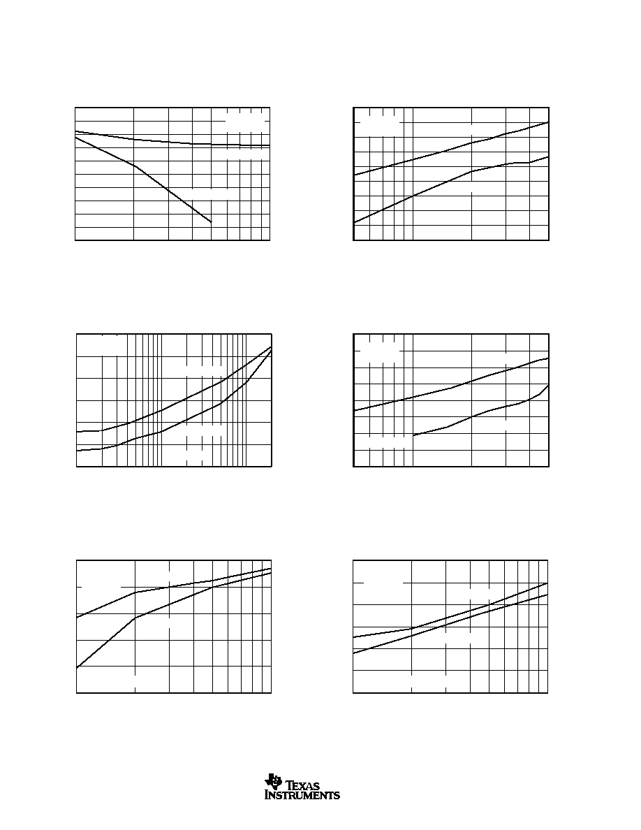
HARMONIC DISTORTION vs LOAD RESISTANCE
100
1k
Resistance (
)
Harmonic Distortion (dBc)
≠60
≠65
≠70
≠75
≠80
≠85
≠90
≠95
≠100
≠105
≠110
V
O
= 2Vp-p
f = 5MHz
See Figure 1
2nd Harmonic
3rd Harmonic
HARMONIC DISTORTION vs FREQUENCY
0.1
1
20
10
Frequency (MHz)
Harmonic Distortion (dBc)
≠50
≠60
≠70
≠80
≠90
≠100
≠110
3rd Harmonic
2nd Harmonic
V
O
= 2Vp-p
R
L
= 200
See Figure 1
HARMONIC DISTORTION vs NONINVERTING GAIN
1
10
Gain (V/V)
Harmonic Distortion (dBc)
≠60
≠70
≠80
≠90
≠100
≠110
V
O
= 2Vp-p
f = 5MHz
R
L
= 200
See Figure 1, R
G
Adjusted
2nd Harmonic
3rd Harmonic
HARMONIC DISTORTION vs INVERTING GAIN
≠1
≠10
Gain (V/V)
Harmonic Distortion (dBc)
≠60
≠65
≠70
≠75
≠80
≠85
≠90
V
O
= 2Vp-p
R
F
= 604
F = 5MHz
R
L
= 200
See Figure 2, R
G
and R
M
Adjusted
2nd Harmonic
3rd Harmonic
HARMONIC DISTORTION vs OUTPUT VOLTAGE (5MHz)
0.5
1
5
Output Voltage Swing (Vp-p)
Harmonic Distortion (dBc)
≠60
≠65
≠70
≠75
≠80
≠85
≠90
≠95
≠100
≠105
f = 5MHz
R
L
= 200
2nd Harmonic
3rd Harmonic
HARMONIC DISTORTION vs OUTPUT VOLTAGE (1MHz)
0.5
1
5
Output Voltage Swing (Vp-p)
Harmonic Distortion (dBc)
≠70
≠75
≠80
≠85
≠90
≠95
≠100
≠105
≠110
f = 1MHz
R
L
= 200
See Figure 1
2nd Harmonic
3rd Harmonic

OPA656
7
SBOS196B
www.ti.com
TYPICAL CHARACTERISTICS: V
S
=
±
5V
(Cont.)
T
A
= +25
∞
C, G
= +2, R
F
= 250
, R
L
= 100
, unless otherwise noted.
INPUT CURRENT AND VOLTAGE NOISE DENSITY
10
100
1k
10k
100k
1M
10M
f (Hz)
en (nV/
Hz)
in (fA/
Hz)
100
10
1
Input Voltage Noise 7nV/
Hz
Input Current Noise 1.3fA/
Hz
COMMON-MODE REJECTION RATIO AND
POWER-SUPPLY REJECTION RATIO vs FREQUENCY
1k
100k
1M
10M
10k
100M
Frequency (Hz)
CMRR (dB)
PSRR (dB)
110
100
90
80
70
60
50
40
30
20
CMRR
+PSRR
≠PSRR
OPEN-LOOP GAIN AND PHASE
1k
100
100k
1M
10M
10k
1G
100M
Frequency (Hz)
Open-Loop Gain (dB)
Open-Loop Phase (30
∞
/div)
70
60
50
40
30
20
10
0
0
≠30
≠60
≠90
≠120
≠150
≠180
≠210
20 log(A
OL
)
< A
OL
RECOMMENDED R
S
vs CAPACITIVE LOAD
10
100
1k
Capacitive Load (pF)
R
S
(
)
100
10
1
For Maximally Flat Frequency Response
FREQUENCY RESPONSE vs CAPACITIVE LOAD
1
10
100
500
Frequency (MHz)
Normalized Gain to Capacitive Load (dB)
9
6
3
0
≠3
≠6
≠9
≠12
R
S
50
1k
V
I
V
O
C
L
250
250
OPA656
C
L
= 22pF
C
L
= 100pF
C
L
= 10pF
2-TONE, 3RD-ORDER
INTERMODULATION SPURIOUS
≠10
≠8
≠6
≠4
≠2
4
2
0
6
8
Single-Tone Load Power (dBm)
3rd-Order Spurious Level (dBc)
60
55
50
45
40
35
30
25
20
50
50
50
P
I
P
O
402
402
OPA656
5MHz
2MHz
15MHz
10MHz
OPA656
8
SBOS196B
www.ti.com
TYPICAL CHARACTERISTICS: V
S
=
±
5V
(Cont.)
T
A
= +25
∞
C, G
= +2, R
F
= 250
, R
L
= 100
, unless otherwise noted.
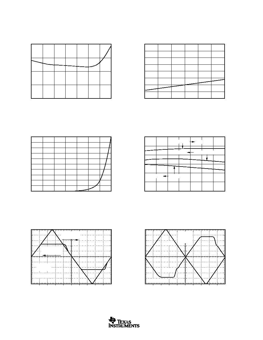
INVERTING OVERDRIVE RECOVERY
Time (20ns/div)
5
4
3
2
1
0
≠1
≠2
≠3
≠4
≠5
R
L
= 100
R
F
= 402
G = ≠1
See Figure 2
Output
Input
Input and Output V
oltage (V)
NONINVERTING INPUT OVERDRIVE RECOVERY
Time (20ns/div)
Output V
oltage (V)
Input V
oltage (V)
8.0
6.4
4.8
3.2
1.6
0
≠1.6
≠3.2
≠4.8
≠6.4
≠8.0
4.0
3.2
2.4
1.6
0.8
0
≠0.8
≠1.6
≠2.4
≠3.2
≠4.0
R
L
= 100
G = +2
See Figure 1
Output Voltage
Left Scale
Input Voltage
Right Scale
SUPPLY AND OUTPUT CURRENT vs TEMPERATURE
≠50
≠25
0
25
50
75
100
125
Ambient Temperature (
∞
C)
Output Current (25mA/div)
Supply Current (3mA/div)
150
125
100
75
50
25
0
18
15
12
9
6
3
0
Supply Current
Right Scale
Left Scale
Sourcing Current
Sinking Current
Left Scale
TYPICAL INPUT BIAS CURRENT DRIFT
OVER TEMPERATURE
≠50
≠25
0
25
50
75
100
125
Ambient Temperature (
∞
C)
Input Bias Current (pA)
1000
900
800
700
600
500
400
300
200
100
0
TYPICAL INPUT BIAS CURRENT
vs COMMON-MODE INPUT VOLTAGE
≠3
≠2
≠1
0
1
2
3
Common-Mode Input Voltage (V)
Input Bias Current (pA)
2.0
1.5
1.0
0.5
0
≠0.5
≠1.0
≠1.5
≠2.0
TYPICAL INPUT OFFSET VOLTAGE DRIFT
OVER TEMPERATURE
≠50
≠25
0
25
50
75
100
125
Ambient Temperature (
∞
C)
Input Of
fset V
oltage (mV)
1.0
0.5
0
≠0.5
≠1.0

OPA656
9
SBOS196B
www.ti.com
TYPICAL CHARACTERISTICS: V
S
=
±
5V
(Cont.)
T
A
= +25
∞
C, G
= +2, R
F
= 250
, R
L
= 100
, unless otherwise noted.
COMMON-MODE REJECTION RATIO
vs COMMON-MODE INPUT VOLTAGE
≠5
≠4
≠3
≠2
≠1
5
4
3
2
1
0
Common-Mode Input Voltage (V)
CMRR (dB)
110
90
70
50
CLOSED-LOOP OUTPUT IMPEDANCE
vs FREQUENCY
1k
10k
100k
1M
10M
100M
Frequency (Hz)
Output Impedance (
)
10
1
0.1
0.01
OUTPUT VOLTAGE AND CURRENT LIMITATIONS
≠100 ≠80
≠60 ≠40
≠20
0
20
40
60
80
100
I
O
(mA)
V
O
(V)
5
4
3
2
1
0
≠1
≠2
≠3
≠4
≠5
1W Internal Power
R
L
= 100
R
L
= 50
R
L
= 25
1W Internal Power
OPA656
10
SBOS196B
www.ti.com
APPLICATIONS INFORMATION
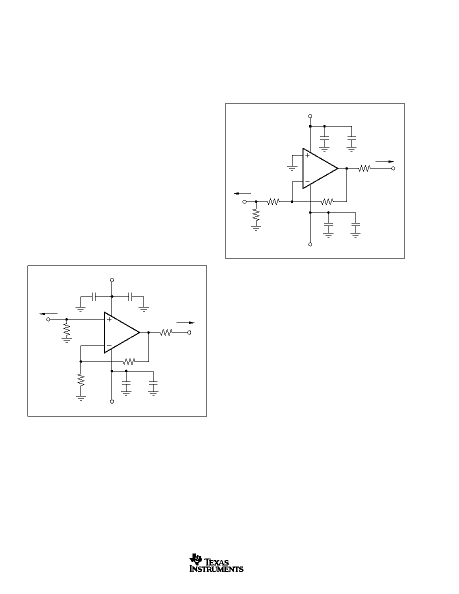
WIDEBAND, NONINVERTING OPERATION
The OPA656 provides a unique combination of a broadband,
unity gain stable, voltage-feedback amplifier with the DC
precision of a trimmed JFET-input stage. Its very high Gain
Bandwidth Product (GBP) of 230MHz can be used to either
deliver high signal bandwidths for low-gain buffers, or to
deliver broadband, low-noise transimpedance bandwidth to
photodiode-detector applications. To achieve the full perfor-
mance of the OPA656, careful attention to PC board layout
and component selection is required as discussed in the
remaining sections of this data sheet.
Figure 1 shows the noninverting gain of +2 circuit used as the
basis for most of the Typical Characteristics. Most of the curves
were characterized using signal sources with 50
driving im-
pedance, and with measurement equipment presenting a 50
load impedance. In Figure 1, the 50
shunt resistor at the V
I
terminal matches the source impedance of the test generator,
while the 50
series resistor at the V
O
terminal provides a
matching resistor for the measurement equipment load. Gener-
ally, data sheet voltage swing specifications are at the output pin
(V
O
in Figure 1) while output power specifications are at the
matched 50
load. The total 100
load at the output combined
with the 500
total feedback network load, presents the OPA656
with an effective output load of 83
for the circuit of Figure 1.
WIDEBAND, INVERTING GAIN OPERATION
The circuit of Figure 2 shows the inverting gain of ≠1 test
circuit used for most of the inverting Typical Characteristics.
In this case, an additional resistor R
M
is used to achieve the
50
input impedance required by the test equipment using in
characterization. This input impedance matching is optional
in a circuit board environment where the OPA656 is used as
an inverting amplifier at the output of a prior stage.
FIGURE 1. Noninverting G = +2 Specifications and Test
Circuit.
Voltage-feedback op amps, unlike current feedback prod-
ucts, can use a wide range of resistor values to set their gain.
To retain a controlled frequency response for the noninverting
voltage amplifier of Figure 1, the parallel combination of
R
F
|| R
G
should always < 200
. In the noninverting configu-
ration, the parallel combination of R
F
|| R
G
will form a pole
with the parasitic input capacitance at the inverting node of
the OPA656 (including layout parasitics). For best perfor-
mance, this pole should be at a frequency greater than the
closed loop bandwidth for the OPA656. For this reason, a
direct short from output to inverting input is recommended for
the unity gain follower application.
In this configuration, the output sees the feedback resistor as
an additional load in parallel with the 100
load used for test.
It is often useful to increase the R
F
value to decrease the
loading on the output (improving harmonic distortion) with the
constraint that the parallel combination of R
F
|| R
G
< 200
.
For higher inverting gains with the DC precision provided by
the FET input OPA656, consider the higher gain bandwidth
product OPA657.
Figure 2 also shows the noninverting input tied directly to
ground. Often, a bias current canceling resistor to ground is
included here to null out the DC errors caused by input bias
current effects. This is only useful when the input bias
currents are matched. For a JFET part like the OPA656, the
input bias currents do not match but are so low to begin with
(< 5pA) that DC errors due to input bias currents are
negligible. Hence, no resistor is recommended at the
noninverting inputs for the inverting signal path condition.
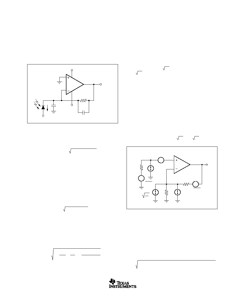
WIDEBAND, HIGH SENSITIVITY, TRANSIMPEDANCE
DESIGN
The high GBP and low input voltage and current noise for the
OPA656 make it an ideal wideband transimpedance ampli-
fier for low to moderate transimpedance gains. Higher
transimpedance gains (> 100k
) will benefit from the low
input noise current of a FET input op amp such as the
OPA656. One transimpedance design example is shown on
the front page of the data sheet. Designs that require high
bandwidth from a large area detector will benefit from the low
input voltage noise for the OPA656. This input voltage noise
FIGURE 2. Inverting G = ≠1 Specifications and Test Circuit.
OPA656
+5V
≠5V
≠V
S
+V
S
50
V
O
V
I
50
+
0.1
µ
F
+
6.8
µ
F
6.8
µ
F
R
G
250
R
F
250
50
Source
50
Load
0.1
µ
F
OPA656
+5V
≠5V
+V
S
≠V
S
R
M
57.6
50
V
O
V
I
+
6.8
µ
F
0.1
µ
F
+
6.8
µ
F
0.1
µ
F
R
F
402
R
G
402
50
Source
50
Load
OPA656
11
SBOS196B
www.ti.com
is peaked up over frequency by the diode source capaci-
tance, and can, in many cases, become the limiting factor to
input sensitivity. The key elements to the design are the
expected diode capacitance (C
D
) with the reverse bias volt-
age (≠V
B
) applied, the desired transimpedance gain, R
F
, and
the GBP for the OPA656 (230MHz). Figure 3 shows a design
from a 25pF source capacitance diode through a 50k
transimpedance gain. With these 3 variables set (including
the parasitic input capacitance for the OPA656 added to C
D
),
the feedback capacitor value (C
F
) may be set to control the
frequency response.
Where:
i
EQ
= Equivalent input noise current if the output noise is
bandlimited to F < 1/(2
R
F
C
D
).
i
N
= Input current noise for the op amp inverting input.
e
N
= Input voltage noise for the op amp.
C
D
= Diode capacitance.
F = Bandlimiting frequency in Hz (usually a postfilter prior
to further signal processing).
4kT = 1.6E ≠ 20J at 290
∞
K.
Evaluating this expression up to the feedback pole frequency
at 3.8MHz for the circuit of Figure 3, gives an equivalent input
noise current of 2.7pA/ Hz . This is much higher than the
1.3fA/ Hz for just the op amp itself. This result is being
dominated by the last term in the equivalent input noise
current expression. It is essential in this case to use a low
voltage noise op amp.
OPERATING SUGGESTIONS
SETTING RESISTOR VALUES TO MINIMIZE NOISE
The OPA656 provides a very low input noise voltage while
requiring a low 14mA quiescent supply current. To take full
advantage of this low input noise, careful attention to the other
possible noise contributors is required. Figure 4 shows the op
amp noise analysis model with all the noise terms included. In
this model, all the noise terms are taken to be noise voltage or
current density terms in either nV/ Hz or pA/ Hz .
To achieve a maximally flat 2nd-order Butterworth frequency
response, the feedback pole should be set to:
1 2
4
/(
)
(
/(
))
R C
GPB
R C
F F
F D
=
Adding the common mode and differential mode input ca-
pacitance (0.7 + 2.8)pF to the 25pF diode source capaci-
tance of Figure 3, and targeting a 50k
transimpedance gain
using the 230MHz GBP for the OPA656 will require a
feedback pole set to 3.8MHz. This will require a total feed-
back capacitance of 0.8pF. Typical surface-mount resistors
have a parasitic capacitance of 0.2pF leaving the required
0.6pF value shown in Figure 3 to get the required feedback
pole.
This will give an approximate ≠3dB bandwidth set by:
f
GPB
R C
Hz
dB
F D
-
=
3
2
/
)
The example of Figure 3 will give approximately 5.7MHz flat
bandwidth using the 0.6pF feedback compensation.
If the total output noise is bandlimited to a frequency less
than the feedback pole frequency (1/R
F
C
F
), a very simple
expression for the equivalent input noise current can be
derived as:
I
I
kT
R
E
R
E
C F
EQ
N
F
N
F
N
D
=
+
+
+
(
)
2
2
2
4
2
3
FIGURE 3. Wideband, Low-Noise, Transimpendance Amplifier.
FIGURE 4. Op Amp Noise Analysis Model.
The total output spot noise voltage can be computed as the
square root of the squared contributing terms to the output
noise voltage. This computation is adding all the contributing
noise powers at the output by superposition, then taking the
square root to get back to a spot noise voltage. Equation 1
shows the general form for this output noise voltage using
the terms shown in Figure 4.
(1)
E
E
I
R
kTR
NG
I R
kTR NG
O
NI
BN S
S
BI F
F
=
+
(
)
+
+
(
)
+
2
2
2
2
4
4
R
F
50k
Supply Decoupling
Not Shown
C
D
25pF
OPA656
+5V
≠5V
≠V
B
I
D
V
O
=
I
D
R
F
C
F
0.6pF
4kT
R
G
R
G
R
F
R
S
OPA656
I
BI
E
O
I
BN
4kT = 1.6E ≠20J
at 290
∞
K
E
RS
E
NI
4kTR
S
4kTR
F
*
*
*

OPA656
12
SBOS196B
www.ti.com
Dividing this expression by the noise gain (G
N
= 1+R
F
/R
G
)
will give the equivalent input referred spot noise voltage at
the noninverting input as shown in Equation 2.
(2)
E
E
I
R
kTR
I R
NG
kTR
NG
N
NI
BN S
S
BI F
F
=
+
(
)
+
+
+
2
2
2
4
4
Putting high resistor values into Equation 2 can quickly
dominate the total equivalent input referred noise. A source
impedance on the noninverting input of 3k
will add a
Johnson voltage noise term equal to just that for the amplifier
itself (7nV/ Hz). While the JFET input of the OPA656 is ideal
for high source impedance applications, both the overall
bandwidth and noise will be limited by higher source imped-
ances in the noninverting configuration of Figure 1.
FREQUENCY RESPONSE CONTROL
Voltage-feedback op amps like the OPA656 exhibit decreas-
ing signal bandwidth as the signal gain is increased. In
theory, this relationship is described by the GBP shown in the
Electrical Characteristics. Ideally, dividing GBP by the
noninverting signal gain (also called the Noise Gain, or NG)
will predict the closed-loop bandwidth. In practice, this only
holds true when the phase margin approaches 90
∞
, as it does
in high-gain configurations. At low gains (increased feedback
factors), most high-speed amplifiers will exhibit a more com-
plex response with lower phase margin. The OPA656 is
compensated to give a maximally flat 2nd-order Butterworth
closed loop response at a noninverting gain of +2 (Figure 1).
This results in a typical gain of +2 bandwidth of 200MHz, far
exceeding that predicted by dividing the 230MHz GBP by 2.
Increasing the gain will cause the phase margin to approach
90
∞
and the bandwidth to more closely approach the pre-
dicted value of (GBP/NG). At a gain of +10 the OPA656 will
show the 23MHz bandwidth predicted using the simple
formula and the typical GBP of 230MHz.
Unity-gain stable op amps like the OPA656 can also be
bandlimited using a capacitor across the feedback resistor.
For the noninverting configuration of Figure 1, a capacitor
across the feedback resistor will decrease the gain with
frequency down to a gain of +1. For instance, to bandlimit the
gain of +2 design to 20MHz, a 32pF capacitor can be placed
in parallel with the 250
feedback resistor. This will, how-
ever, only decrease the gain from 2 to 1. Using a feedback
capacitor to limit the signal bandwidth is more effective in the
inverting configuration of Figure 2. Adding that same capaci-
tor to the feedback of Figure 2 will set a pole in the signal
frequency response at 20MHz, but in this case it will continue
to attenuate the signal gain to below 1. However, the output
noise contribution due the input voltage noise of the OPA656
will still only be reduced to a gain of 1 with the addition of the
feedback capacitor.
DRIVING CAPACITIVE LOADS
One of the most demanding and yet very common load
conditions for an op amp is capacitive loading. Often, the
capacitive load is the input of an ADC--including additional
external capacitance which may be recommended to im-
prove ADC linearity. A high-speed, high open-loop gain
amplifier like the OPA656 can be very susceptible to de-
creased stability and closed-loop response peaking when a
capacitive load is placed directly on the output pin. When the
amplifier's open loop output resistance is considered, this
capacitive load introduces an additional pole in the signal
path that can decrease the phase margin. Several external
solutions to this problem have been suggested. When the
primary considerations are frequency response flatness, pulse
response fidelity and/or distortion, the simplest and most
effective solution is to isolate the capacitive load from the
feedback loop by inserting a series isolation resistor between
the amplifier output and the capacitive load. This does not
eliminate the pole from the loop response, but rather shifts it
and adds a zero at a higher frequency. The additional zero
acts to cancel the phase lag from the capacitive load pole,
thus increasing the phase margin and improving stability.
The Typical Characteristics show the recommended R
S
ver-
sus Capacitive Load and the resulting frequency response at
the load. In this case, a design target of a maximally flat
frequency response was used. Lower values of R
S
may be
used if some peaking can be tolerated. Also, operating at
higher gains (than the +2 used in the Typical Characteristics)
will require lower values of R
S
for a minimally peaked
frequency response. Parasitic capacitive loads greater than
2pF can begin to degrade the performance of the OPA656.
Long PC board traces, unmatched cables, and connections
to multiple devices can easily cause this value to be ex-
ceeded. Always consider this effect carefully, and add the
recommended series resistor as close as possible to the
OPA656 output pin (see Board Layout section).
DISTORTION PERFORMANCE
The OPA656 is capable of delivering a low distortion signal
at high frequencies over a wide range of gains. The distortion
plots in the Typical Characteristics show the typical distortion
under a wide variety of conditions.
Generally, until the fundamental signal reaches very high
frequencies or powers, the 2nd-harmonic will dominate the
distortion with negligible 3rd-harmonic component. Focusing
then on the 2nd-harmonic, increasing the load impedance
improves distortion directly. Remember that the total load
includes the feedback network--in the noninverting configura-
tion this is sum of R
F
+ R
G
, while in the inverting configuration
this is just R
F
(see Figure 1). Increasing output voltage swing
increases harmonic distortion directly. A 6dB increase in
output swing will generally increase the 2nd-harmonic 12dB
and the 3rd-harmonic 18dB. Increasing the signal gain will also

OPA656
13
SBOS196B
www.ti.com
increase the 2nd-harmonic distortion. Again a 6dB increase in
gain will increase the 2nd- and 3rd-harmonic by about 6dB
even with a constant output power and frequency. And finally,
the distortion increases as the fundamental frequency in-
creases due to the rolloff in the loop gain with frequency.
Conversely, the distortion will improve going to lower frequen-
cies down to the dominant open loop pole at approximately
100kHz. Starting from the ≠70dBc 2nd-harmonic for a 5MHz,
2Vp-p fundamental into a 200
load at G = +2 (from the
Typical Characteristics), the 2nd-harmonic distortion for fre-
quencies lower than 100kHz will be < ≠105dBc.
The OPA656 has an extremely low 3rd-order harmonic
distortion. This also shows up in the 2-tone 3rd-order inter-
modulation spurious (IM3) response curves. The 3rd-order
spurious levels are extremely low (< ≠80dBc) at low output
power levels. The output stage continues to hold them low
even as the fundamental power reaches higher levels. As the
Typical Characteristics show, the spurious intermodulation
powers do not increase as predicted by a traditional intercept
model. As the fundamental power level increases, the dy-
namic range does not decrease significantly. For 2 tones
centered at 10MHz, with 4dBm/tone into a matched 50
load
(i.e., 1Vp-p for each tone at the load, which requires 4Vp-p
for the overall 2-tone envelope at the output pin), the Typical
Characteristics show a 78dBc difference between the test
tone and the 3rd-order intermodulation spurious levels. This
exceptional performance improves further when operating at
lower frequencies and/or higher load impedances.
DC ACCURACY AND OFFSET CONTROL
The OPA656 can provide excellent DC accuracy due to its
high open-loop gain, high common-mode rejection, high
power-supply rejection, and its trimmed input offset voltage
(and drift) along with the negligible errors introduced by the
low input bias current. For the best DC precision, a high-
grade version (OPA656UB or OPA656NB) screens the key
DC parameters to an even tighter limits. Both standard- and
high-grade versions take advantage of a new final test
technique to 100% test input offset voltage drift over tem-
perature. This discussion will use the high-grade typical and
min/max electrical characteristics for illustration, however, an
identical analysis applies to the standard-grade version.
The total output DC offset voltage in any configuration and
temperature will be the combination of a number of possible
error terms. In a JFET part like the OPA656, the input bias
current terms are typically quite low but are unmatched.
Using bias current cancellation techniques, more typical in
bipolar input amplifiers, does not improve output DC offset
errors. Errors due to the input bias current will only become
dominant at elevated temperatures. The OPA656 shows the
typical 2x increase in every 10
∞
C common to JFET-input
stage amplifiers. Using the 5pA maximum tested value at
25
∞
C, and a 20
∞
C internal self heating (see thermal analysis),
the maximum input bias current at 85
∞
C ambient will be
5pA ∑ 2
(105 ≠ 25)/10
= 1280pA. For noninverting configurations,
this term only begins to be a significant term versus the input
offset voltage for source impedances > 750k
. This would
also be the feedback-resistor value for transimpedance ap-
plications (see Figure 3) where the output DC error due to
inverting input bias current is on the order of that contributed
by the input offset voltage. In general, except for these
extremely high impedance values, the output DC errors due
to the input bias current may be neglected.
After the input offset voltage itself, the most significant term
contributing to output offset voltage is the PSRR for the
negative supply. This term is modeled as an input offset
voltage shift due to changes in the negative power-supply
voltage (and similarly for the +PSRR). The high-grade test
limit for ≠PSRR is 62dB. This translates into 1.59mV/V input
offset voltage shift = 10
(≠62/20)
. In the worst case, a
±
0.38V
(
±
7.6%) shift in the negative supply voltage will produce a
±
0.6mV apparent input offset voltage shift. Since this is
comparable to the tested limit of
±
0.6mV input offset voltage,
a careful control of the negative supply voltage is required.
The +PSRR is tested to a minimum value of 74dB. This
translates into 10
(≠74/20)
= 0.2mV/V sensitivity for the input
offset voltage to positive power supply changes.
As an example, compute the worst-case output DC error for
the transimpedance circuit of Figure 1 at 25
∞
C and then the
shift over the 0
∞
C to 70
∞
C range given the following assump-
tions.
Negative Power Supply
= ≠5V
±
0.2V with a
±
5mV/
∞
C worst-case shift
Positive Power Supply
= +5V
±
0.2V with a
±
5mV/
∞
C worst-case shift
Initial 25
∞
C Output DC Error Band
=
±
0.3mV (due to the ≠PSRR = 1.59mV/V ∑
±
0.2V)
±
0.04mV (due to the +PSRR = 0.2mV/V ∑
±
0.2V)
±
0.6mV Input Offset Voltage
Total =
±
0.94mV
This would be the worst-case error band in volume produc-
tion at 25
∞
C acceptance testing given the conditions stated.
Over the temperature range of 0
∞
C to 70
∞
C, we can expect
the following worst-case shifting from initial value. A 20
∞
C
internal junction self heating is assumed here.
±
0.36mV (OPA656 high-grade input offset drift)
=
±
6
µ
V/
∞
C ∑ (70
∞
C + 20
∞
C ≠ 25
∞
C))
±
0.23mV (≠PSRR of 60dB with 5mV ∑ (70
∞
C ≠ 25
∞
C) supply shift)
±
0.06mV (+PSRR of 72dB with 5mV ∑ (70
∞
C ≠ 25
∞
C) supply shift)
Total =
±
0.65mV
This would be the worst-case shift from initial offset over a
0
∞
C to 70
∞
C ambient for the conditions stated. Typical initial
output DC error bands and shifts over temperature will be
much lower than these worst-case estimates.
In the transimpedance configuration, the CMRR errors can be
neglected since the input common mode voltage is held at
ground. For noninverting gain configurations (see Figure 1), the
CMRR term will need to be considered but will typically be far
lower than the input offset voltage term. With a tested minimum
of 80dB (100uV/V), the added apparent DC error will be no more
than
±
0.2mV for a
±
2V input swing to the circuit of Figure 1.

OPA656
14
SBOS196B
www.ti.com
POWER-SUPPLY CONSIDERATIONS
The OPA656 is intended for operation on
±
5V supplies.
Single-supply operation is allowed with minimal change from
the stated specifications and performance from a single
supply of +8V to +12V maximum. The limit to lower supply
voltage operation is the useable input voltage range for the
JFET-input stage. Operating from a single supply of +12V
can have numerous advantages. With the negative supply at
ground, the DC errors due to the ≠PSRR term can be
minimized. Typically, AC performance improves slightly at
+12V operation with minimal increase in supply current.
THERMAL ANALYSIS
The OPA656 will not require heatsinking or airflow in most
applications. Maximum allowed junction temperature will set
the maximum allowed internal power dissipation as de-
scribed below. In no case should the maximum junction
temperature be allowed to exceed 150
∞
C.
Operating junction temperature (T
J
) is given by T
A
+ P
D
∑
JA
.
The total internal power dissipation (P
D
) is the sum of quiescent
power (P
DQ
) and additional power dissipated in the output stage
(P
DL
) to deliver load power. Quiescent power is simply the
specified no-load supply current times the total supply voltage
across the part. P
DL
will depend on the required output signal
and load but would, for a grounded resistive load, be at a
maximum when the output is fixed at a voltage equal to 1/2 of
either supply voltage (for equal bipolar supplies). Under this
condition P
DL
= V
S
2
/(4 ∑ R
L
) where R
L
includes feedback
network loading.
Note that it is the power in the output stage and not into the
load that determines internal power dissipation.
As a worst-case example, compute the maximum T
J
using an
OPA656N (SOT23-5 package) in the circuit of Figure 1
operating at the maximum specified ambient temperature of
+85
∞
C and driving a grounded 100
load.
P
D
= 10V ∑ 16.1mA + 5
2
/(4 ∑ (100
|| 800
)) = 231mW
Maximum T
J
= +85
∞
C + (0.23W ∑ 150
∞
C/W) = 120
∞
C.
All actual applications will be operating at lower internal
power and junction temperature.
BOARD LAYOUT
Achieving optimum performance with a high-frequency am-
plifier like the OPA656 requires careful attention to board
layout parasitics and external component types. Recommen-
dations that will optimize performance include:
a) Minimize parasitic capacitance to any AC ground for all
of the signal I/O pins. Parasitic capacitance on the output and
inverting input pins can cause instability--on the noninvert-
ing input, it can react with the source impedance to cause
unintentional bandlimiting. To reduce unwanted capacitance,
a window around the signal I/O pins should be opened in all
of the ground and power planes around those pins. Other-
wise, ground and power planes should be unbroken else-
where on the board.
b) Minimize the distance (< 0.25") from the power-supply
pins to high-frequency 0.1uF decoupling capacitors. At the
device pins, the ground and power plane layout should not
be in close proximity to the signal I/O pins. Avoid narrow
power and ground traces to minimize inductance between
the pins and the decoupling capacitors. The power-supply
connections should always be decoupled with these capaci-
tors. Larger (2.2
µ
F to 6.8
µ
F) decoupling capacitors, effective
at lower frequency, should also be used on the supply pins.
These may be placed somewhat farther from the device and
may be shared among several devices in the same area of
the PC board.
c) Careful selection and placement of external components
will preserve the high frequency performance of the OPA656.
Resistors should be a very low reactance type. Surface-mount
resistors work best and allow a tighter overall layout. Metal film
and carbon composition axially leaded resistors can also pro-
vide good high frequency performance. Again, keep their leads
and PC board trace length as short as possible. Never use
wirewound type resistors in a high frequency application. Since
the output pin and inverting input pin are the most sensitive to
parasitic capacitance, always position the feedback and series
output resistor, if any, as close as possible to the output pin.
Other network components, such as noninverting input termina-
tion resistors, should also be placed close to the package.
Where double side component mounting is allowed, place the
feedback resistor directly under the package on the other side
of the board between the output and inverting input pins. Even
with a low parasitic capacitance shunting the external resistors,
excessively high resistor values can create significant time
constants that can degrade performance. Good axial metal film
or surface-mount resistors have approximately 0.2pF in shunt
with the resistor. For resistor values > 1.5k
, this parasitic
capacitance can add a pole and/or zero below 500MHz that can
effect circuit operation. Keep resistor values as low as possible
consistent with load driving considerations. It has been sug-
gested here that a good starting point for design would be to
keep R
F
|| R
G
< 250
for voltage amplifier applications. Doing
this will automatically keep the resistor noise terms low, and
minimize the effect of their parasitic capacitance.
Transimpedance applications (see Figure 3) can use whatever
feedback resistor is required by the application as long as the
feedback compensation capacitor is set considering all parasitic
capacitance terms on the inverting node.
d) Connections to other wideband devices on the board
may be made with short direct traces or through onboard
transmission lines. For short connections, consider the trace
and the input to the next device as a lumped capacitive load.
Relatively wide traces (50mils to 100mils) should be used,
preferably with ground and power planes opened up around
them. Estimate the total capacitive load and set R
S
from the
plot of "Recommended R
S
vs Capacitive Load." Low parasitic
capacitive loads (< 5pF) may not need an R
S
since the
OPA656 is nominally compensated to operate with a 2pF
parasitic load. Higher parasitic capacitive loads without an R
S
are allowed as the signal gain increases (increasing the
OPA656
15
SBOS196B
www.ti.com
unloaded phase margin) If a long trace is required, and the
6dB signal loss intrinsic to a doubly-terminated transmission
line is acceptable, implement a matched impedance trans-
mission line using microstrip or stripline techniques (consult
an ECL design handbook for microstrip and stripline layout
techniques). A 50
environment is normally not necessary
onboard, and in fact a higher impedance environment will
improve distortion as shown in the distortion versus load
plots. With a characteristic board trace impedance defined
based on board material and trace dimensions, a matching
series resistor into the trace from the output of the OPA656
is used as well as a terminating shunt resistor at the input of
the destination device. Remember also that the terminating
impedance will be the parallel combination of the shunt
resistor and the input impedance of the destination device--
this total effective impedance should be set to match the
trace impedance. If the 6dB attenuation of a doubly-termi-
nated transmission line is unacceptable, a long trace can be
series-terminated at the source end only. Treat the trace as
a capacitive load in this case and set the series resistor value
as shown in the plot of "Recommended R
S
vs Capacitive
Load." This will not preserve signal integrity as well as a
doubly-terminated line. If the input impedance of the destina-
tion device is low, there will be some signal attenuation due
to the voltage divider formed by the series output into the
terminating impedance.
e) Socketing a high speed part like the OPA656 is not
recommended. The additional lead length and pin-to-pin ca-
pacitance introduced by the socket can create an extremely
troublesome parasitic network which can make it almost impos-
sible to achieve a smooth, stable frequency response. Best
results are obtained by soldering the OPA656 onto the board.
FIGURE 5. Internal ESD Protection.
External
Pin
+V
CC
≠V
CC
Internal
Circuitry
INPUT AND ESD PROTECTION
The OPA656 is built using a very high speed complementary
bipolar process. The internal junction breakdown voltages are
relatively low for these very small geometry devices. These
breakdowns are reflected in the Absolute Maximum Ratings
table. All device pins are protected with internal ESD protec-
tion diodes to the power supplies as shown in Figure 5.
These diodes provide moderate protection to input overdrive
voltages above the supplies as well. The protection diodes
can typically support 30mA continuous current. Where higher
currents are possible (e.g. in systems with
±
12V supply parts
driving into the OPA656), current limiting series resistors
should be added into the two inputs. Keep these resistor
values as low as possible since high values degrade both
noise performance and frequency response.
OPA656
16
SBOS196B
www.ti.com
PACKAGE DRAWINGS
MSOI002B ≠ JANUARY 1995 ≠ REVISED SEPTEMBER 2001
D (R-PDSO-G**)
PLASTIC SMALL-OUTLINE PACKAGE
8 PINS SHOWN
8
0.197
(5,00)
A MAX
A MIN
(4,80)
0.189
0.337
(8,55)
(8,75)
0.344
14
0.386
(9,80)
(10,00)
0.394
16
DIM
PINS **
4040047/E 09/01
0.069 (1,75) MAX
Seating Plane
0.004 (0,10)
0.010 (0,25)
0.010 (0,25)
0.016 (0,40)
0.044 (1,12)
0.244 (6,20)
0.228 (5,80)
0.020 (0,51)
0.014 (0,35)
1
4
8
5
0.150 (3,81)
0.157 (4,00)
0.008 (0,20) NOM
0
∞
≠ 8
∞
Gage Plane
A
0.004 (0,10)
0.010 (0,25)
0.050 (1,27)
NOTES: A. All linear dimensions are in inches (millimeters).
B. This drawing is subject to change without notice.
C. Body dimensions do not include mold flash or protrusion, not to exceed 0.006 (0,15).
D. Falls within JEDEC MS-012

OPA656
17
SBOS196B
www.ti.com
PACKAGE DRAWINGS (Cont.)
MPDS018D ≠ FEBRUARY 1996 ≠ REVISED JANUARY 2001
DBV (R-PDSO-G5)
PLASTIC SMALL-OUTLINE
0,10
M
0,20
0,95
0
∞
≠8
∞
0,25
0,35
0,55
Gage Plane
0,15 NOM
4073253-4/F 10/00
2,60
3,00
0,50
0,30
1,50
1,70
4
5
3
1
2,80
3,00
0,95
1,45
0,05 MIN
Seating Plane
NOTES: A. All linear dimensions are in millimeters.
B. This drawing is subject to change without notice.
C. Body dimensions do not include mold flash or protrusion.
D. Falls within JEDEC MO-178

PACKAGING INFORMATION
ORDERABLE DEVICE
STATUS(1)
PACKAGE TYPE
PACKAGE DRAWING
PINS
PACKAGE QTY
OPA656N/250
ACTIVE
SOP
DBV
5
250
OPA656N/3K
ACTIVE
SOP
DBV
5
3000
OPA656NB/250
ACTIVE
SOP
DBV
5
250
OPA656NB/3K
ACTIVE
SOP
DBV
5
3000
OPA656U
ACTIVE
SOIC
D
8
100
OPA656U/2K5
ACTIVE
SOIC
D
8
2500
OPA656UB
ACTIVE
SOIC
D
8
100
OPA656UB/2K5
ACTIVE
SOIC
D
8
2500
(1) The marketing status values are defined as follows:
ACTIVE: Product device recommended for new designs.
LIFEBUY: TI has announced that the device will be discontinued, and a lifetime-buy period is in effect.
NRND: Not recommended for new designs. Device is in production to support existing customers, but TI does not recommend using this part in
a new design.
PREVIEW: Device has been announced but is not in production. Samples may or may not be available.
OBSOLETE: TI has discontinued the production of the device.
PACKAGE OPTION ADDENDUM
www.ti.com
3-Oct-2003

IMPORTANT NOTICE
Texas Instruments Incorporated and its subsidiaries (TI) reserve the right to make corrections, modifications,
enhancements, improvements, and other changes to its products and services at any time and to discontinue
any product or service without notice. Customers should obtain the latest relevant information before placing
orders and should verify that such information is current and complete. All products are sold subject to TI's terms
and conditions of sale supplied at the time of order acknowledgment.
TI warrants performance of its hardware products to the specifications applicable at the time of sale in
accordance with TI's standard warranty. Testing and other quality control techniques are used to the extent TI
deems necessary to support this warranty. Except where mandated by government requirements, testing of all
parameters of each product is not necessarily performed.
TI assumes no liability for applications assistance or customer product design. Customers are responsible for
their products and applications using TI components. To minimize the risks associated with customer products
and applications, customers should provide adequate design and operating safeguards.
TI does not warrant or represent that any license, either express or implied, is granted under any TI patent right,
copyright, mask work right, or other TI intellectual property right relating to any combination, machine, or process
in which TI products or services are used. Information published by TI regarding third-party products or services
does not constitute a license from TI to use such products or services or a warranty or endorsement thereof.
Use of such information may require a license from a third party under the patents or other intellectual property
of the third party, or a license from TI under the patents or other intellectual property of TI.
Reproduction of information in TI data books or data sheets is permissible only if reproduction is without
alteration and is accompanied by all associated warranties, conditions, limitations, and notices. Reproduction
of this information with alteration is an unfair and deceptive business practice. TI is not responsible or liable for
such altered documentation.
Resale of TI products or services with statements different from or beyond the parameters stated by TI for that
product or service voids all express and any implied warranties for the associated TI product or service and
is an unfair and deceptive business practice. TI is not responsible or liable for any such statements.
Following are URLs where you can obtain information on other Texas Instruments products and application
solutions:
Products
Applications
Amplifiers
amplifier.ti.com
Audio
www.ti.com/audio
Data Converters
dataconverter.ti.com
Automotive
www.ti.com/automotive
DSP
dsp.ti.com
Broadband
www.ti.com/broadband
Interface
interface.ti.com
Digital Control
www.ti.com/digitalcontrol
Logic
logic.ti.com
Military
www.ti.com/military
Power Mgmt
power.ti.com
Optical Networking
www.ti.com/opticalnetwork
Microcontrollers
microcontroller.ti.com
Security
www.ti.com/security
Telephony
www.ti.com/telephony
Video & Imaging
www.ti.com/video
Wireless
www.ti.com/wireless
Mailing Address:
Texas Instruments
Post Office Box 655303 Dallas, Texas 75265
Copyright
2003, Texas Instruments Incorporated