 | –≠–ª–µ–∫—Ç—Ä–æ–Ω–Ω—ã–π –∫–æ–º–ø–æ–Ω–µ–Ω—Ç: OPA676KG | –°–∫–∞—á–∞—Ç—å:  PDF PDF  ZIP ZIP |

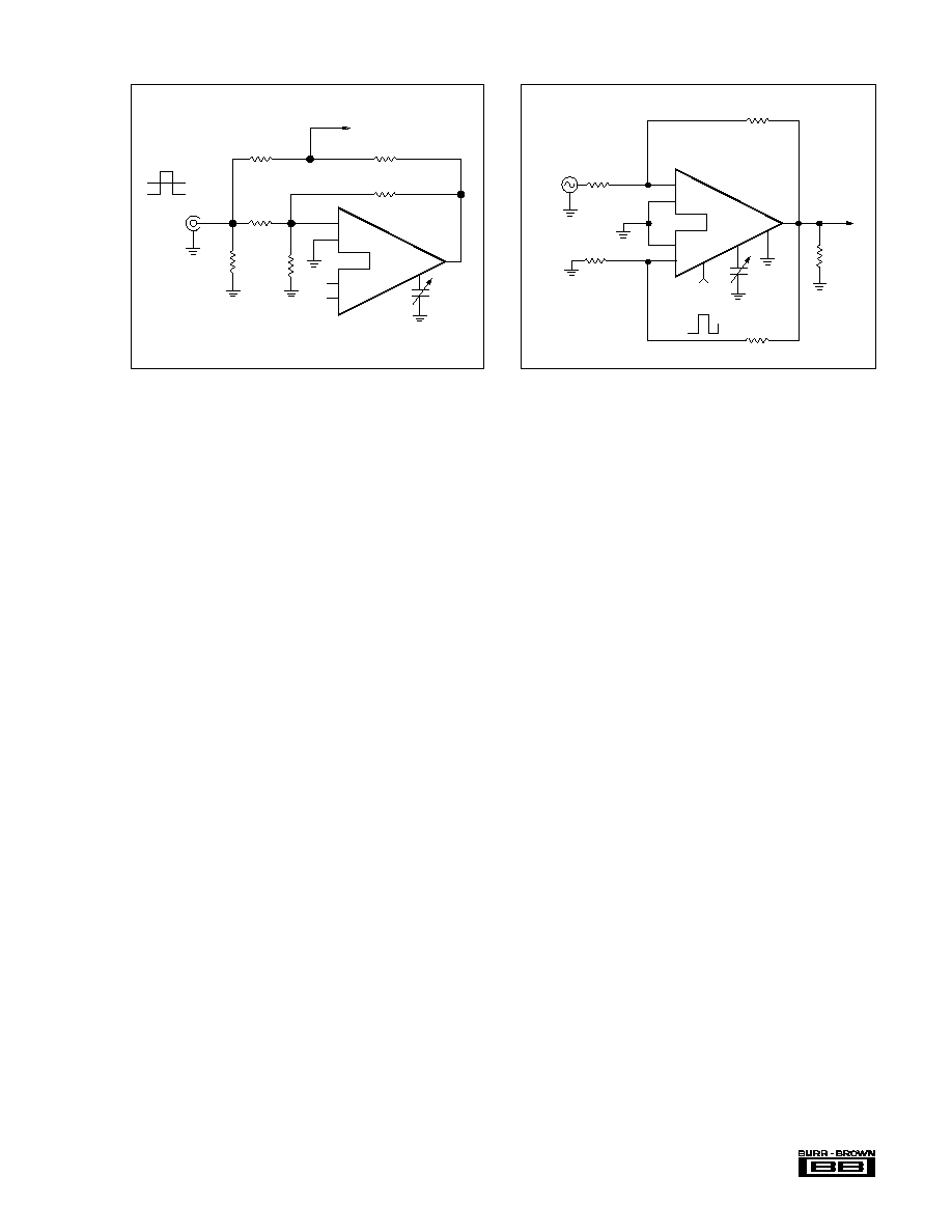
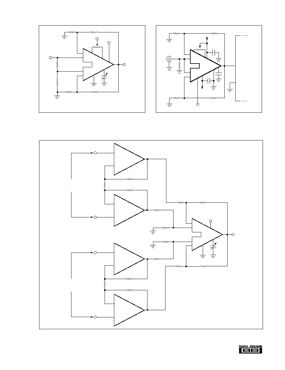
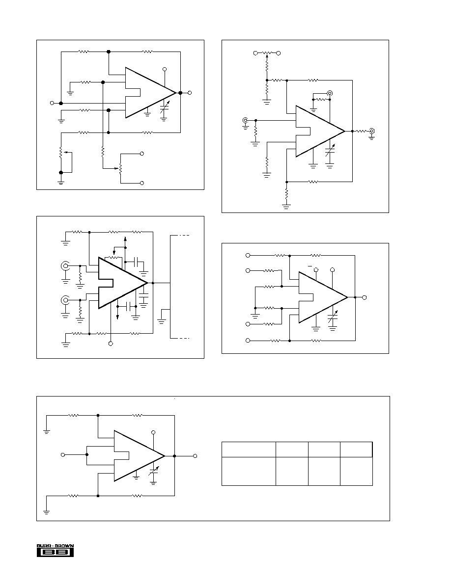
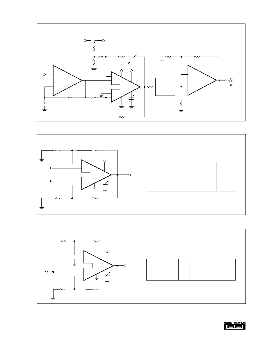
Wideband Switched-Input
OPERATIONAL AMPLIFIER
FEATURES
q
FAST SETTLING: 9ns (1%)
q
WIDE BANDWIDTH: 185MHz (A
V
= 10)
q
LOW OFFSET VOLTAGE:
±
250
µ
V
q
TWO LOGIC SELECTABLE INPUTS
q
FAST INPUT SWITCHING: 8ns (TTL)
q
16-PIN DIP PACKAGE
APPLICATIONS
q
PROGRAMMABLE-GAIN AMPLIFIER
q
FAST 2-INPUT MULTIPLEXER
q
SYNCHRONOUS DEMODULATOR
q
PULSE/RF AMPLIFIERS
q
VIDEO AMPLIFIERS
q
ACTIVE FILTERS
DESCRIPTION
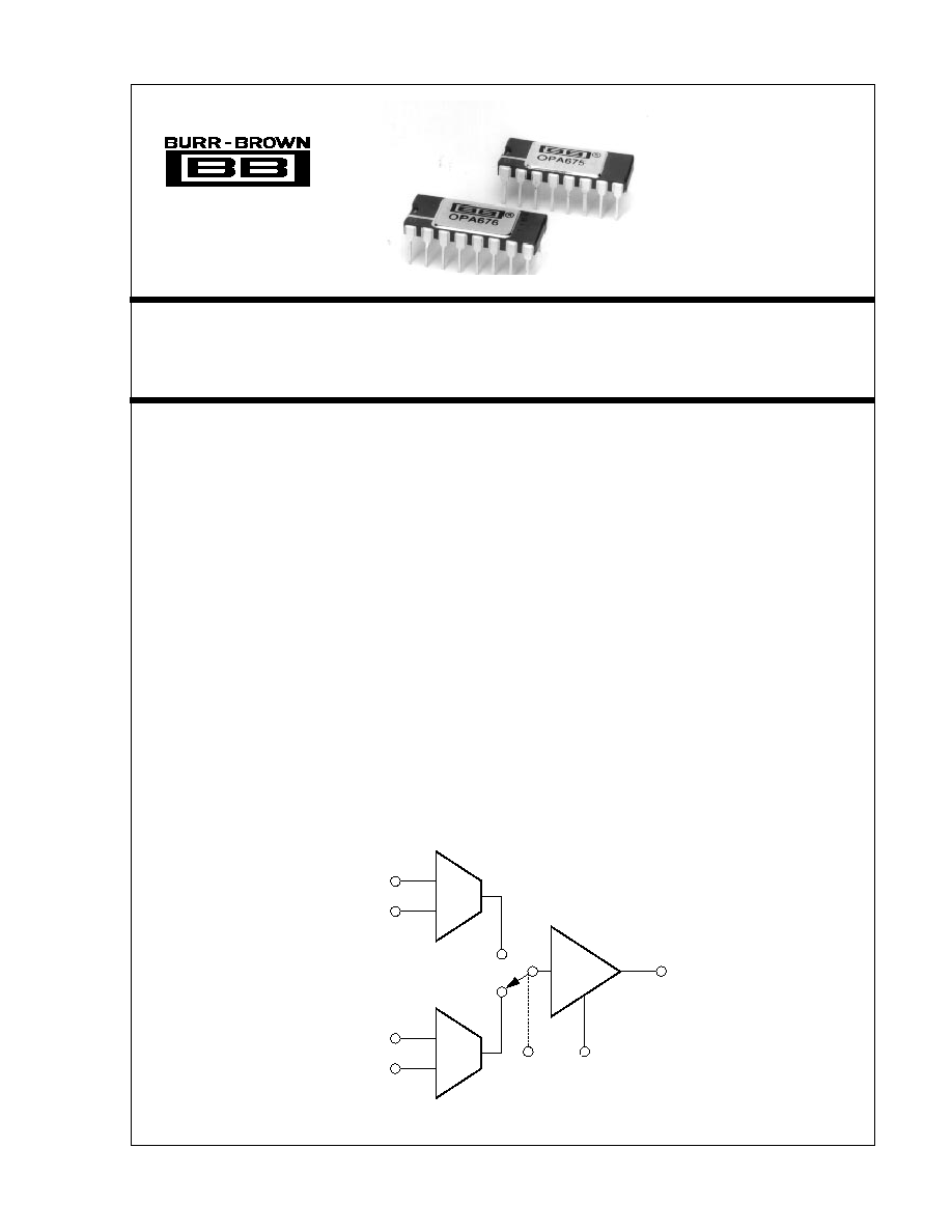
The OPA675 and OPA676 are wideband monolithic
operational amplifiers with two independent differen-
tial inputs. Either input can be selected by an external
logic signal. The OPA675 is compatible with ECL logic
while the OPA676 is TTL compatible. Both amplifiers
are externally compensated and feature very fast input
selection speed: ECL = 4ns, TTL = 6ns. This amplifier
features fully symmetrical differential inputs due to its
"classical" operational amplifier circuit architecture.
Unlike "current-feedback" amplifier designs, the
OPA675/676 may be used in all op amp applications
requiring high speed and precision.
Low distortion and crosstalk make these amplifiers
suitable for RF and video applications.
The OPA675 and OPA676 are available in KG (0
∞
C to
+70
∞
C) and SG (≠55
∞
C to +125
∞
C) grades. All grades
are packaged in a 16-pin DIP.
OPA675
OPA676
+
_
A
TTL: OPA676
ECL: OPA675
B
+
_
Input A
Input B
Output
Compensation
Æ
International Airport Industrial Park ∑ Mailing Address: PO Box 11400 ∑ Tucson, AZ 85734 ∑ Street Address: 6730 S. Tucson Blvd. ∑ Tucson, AZ 85706
Tel: (520) 746-1111 ∑ Twx: 910-952-1111 ∑ Cable: BBRCORP ∑ Telex: 066-6491 ∑ FAX: (520) 889-1510 ∑ Immediate Product Info: (800) 548-6132
©
1988 Burr-Brown Corporation
PDS-864D
Printed in U.S.A. October, 1993

Æ
OPA675/676
2
SPECIFICATIONS
ELECTRICAL
At V
CC
=
±
5VDC, R
L
= 150
, and T
A
= +25
∞
C, unless otherwise noted.
OPA675/676JG, SG
OPA675/676KG
PARAMETER
CONDITIONS
MIN
TYP
MAX
MIN
TYP
MAX
UNITS
INPUT NOISE
(1)
Voltage: f
O
= 10Hz
R
S
= 0
27
*
nV/
Hz
f
O
= 100Hz
10
*
nV/
Hz
f
O
= 1kHz
3.8
*
nV/
Hz
f
O
= 10kHz
2.6
*
nV/
Hz
f
O
= 100kHz
2.4
*
nV/
Hz
f
B
= 10Hz to 10MHz
7.9
*
µ
Vrms
Current: f
O
= 10Hz to 1MHz
2.7
*
pA/
Hz
OFFSET VOLTAGE
(1)
Input Offset Voltage
V
CM
= 0VDC
±
500
±
2mV
±
250
±
1mV
µ
V
Average Drift
T
A
= T
MIN
to T
MAX
±
3
±
10
±
1
±
5
µ
V/
∞
C
Supply Rejection
±
V
CC
= 4.5V to 5.5V
65
86
70
*
dB
BIAS CURRENT
(1)
Input Bias Current
V
CM
= 0VDC
23
35
*
30
µ
A
OFFSET CURRENT
(1)
Input Offset Current
V
CM
= 0VDC
0.8
5
*
*
µ
A
INPUT IMPEDANCE
(1)
Differential
4k
2
*
pF
Common-Mode
10
5
5
*
pF
INPUT VOLTAGE RANGE
(1)
Common-Mode Input Range
±
1.25
±
2.5
*
*
V
Common-Mode Rejection
V
IN
=
±
0.5VDC, V
O
=
±
1.25V
75
100
85
*
dB
OPEN LOOP GAIN, DC
(1)
Open-Loop Voltage Gain
65
70
*
*
dB
FREQUENCY RESPONSE
Closed-Loop Bandwidth
Gain = +2V/V
100
*
MHz
Gain = +5V/V
145
*
MHz
Gain = +10V/V
185
*
MHz
Gain = +50V/V
60
*
MHz
Crosstalk
Gain = +10V/V, f = 100kHz
≠100
*
dBC
(2)
f = 1MHz
≠80
*
dBC
f = 10MHz
≠68
*
dBC
f = 100MHz
≠35
*
dBC
Harmonic Distortion: 10MHz
G = +10V/V, R
L
= 50
, V
O
= 0.5Vp-p
Second Harmonic
≠61
*
dBC
Third Harmonic
≠73
*
dBC
Full Power Response
V
O
= 2.5Vp-p, Gain = +10V/V
25
44
30
*
MHz
Slew Rate
Gain = +10V/V
200
350
240
*
V/
µ
s
Settling Time: 1%
9
*
ns
0.1%
Gain = +10V/V
15
*
ns
0.01%
0.625V Output
Step
25
*
ns
INPUT SELECTION
(3)
Transition Time
ECL: OPA675
5
*
ns
50% In to 50% Out
TTL: OPA676
7.5
*
ns
DIGITAL INPUT
TTL Logic Levels: V
IL
Logic "LO"
0
+0.8
*
*
V
V
IH
Logic "HI"
+2.0
+5
*
*
V
I
IL
Logic "LO", V
IL
= 0V
≠0.05
≠0.2
*
*
mA
I
IH
Logic "HI", V
IH
= +2.7V
1
20
*
*
µ
A
ECL Logic Levels: V
IL
Logic "LO"
≠1.81
≠1.475
*
*
V
V
IH
Logic "HI"
≠1.15
≠ 0.88
*
*
V
I
IL
Logic "LO", V
IL
= ≠1.6V
≠50
≠100
*
*
µ
A
I
IH
Logic "HI", V
IH
= ≠1.0V
≠50
≠100
*
*
µ
A
RATED OUTPUT
Voltage Output
R
L
= 150
±
2.1
±
2.6
*
*
V
R
L
= 50
+1.25
+1.8
*
*
V
≠0.95
≠1.1
≠1.0
*
V
Current Output
±
30
*
mA
Output Resistance
1MHz, Open-Loop, C
C
= 5pF
5
*
Load Capacitance Stability
Gain = +2V/V
50
*
pF
Short Circuit Current
Continuous to Gnd
+45
*
mA
≠25
*
mA
* Same specifications as for JG.

Æ
OPA675/676
3
SPECIFICATIONS
(CONT)
ELECTRICAL
At V
CC
=
±
5VDC, R
L
= 150
, and T
A
= +25
∞
C, unless otherwise noted.
OPA675/676JG, SG
OPA675/676KG
PARAMETER
CONDITIONS
MIN
TYP
MAX
MIN
TYP
MAX
UNITS
POWER SUPPLY
Rated Voltage
±
V
CC
5
*
VDC
Derated Performance
±
V
CC
4.5
6.5
*
*
VDC
Current, Quiescent
I
O
= 0mADC
22
30
*
*
mA
TEMPERATURE RANGE
Specification
Ambient Temp JG, KG
0
+70
*
*
∞
C
SG
≠55
+125
∞
C
Operating:
Ambient Temp JG, KG, SG
≠55
+125
*
*
∞
C
JA
125
*
∞
C/W
* Same specifications as for JG.
ELECTRICAL (FULL TEMPERATURE RANGE SPECIFICATIONS)
At V
CC
=
±
5VDC, R
L
= 150
, and T
A
= T
MIN
to T
MAX
, unless otherwise noted.
OPA675/676JG, SG
OPA675/676KG
PARAMETER
CONDITIONS
MIN
TYP
MAX
MIN
TYP
MAX
UNITS
TEMPERATURE RANGE
Specification
Ambient Temp JG, KG
0
+70
*
*
∞
C
SG
≠55
+125
∞
C
OFFSET VOLTAGE
Average Drift
T
A
= T
MIN
to T
MAX
±
3
±
10
±
1
±
5
µ
V/
∞
C
Supply Rejection
±
V
CC
= 4.5V to 5.5V
60
85
65
*
dB
BIAS CURRENT
Input Bias Current
V
CM
= 0VDC
29
50
*
*
µ
A
OFFSET CURRENT
Input Offset Current
V
CM
= 0VDC
0.8
10
*
*
µ
A
INPUT VOLTAGE RANGE
Common-Mode Input Range
±
2.0
±
2.3
*
*
V
Common-Mode Rejection
V
IN
=
±
0.5VDC, V
O
=
±
1.25V
60
80
65
*
dB
OPEN LOOP GAIN, DC
Open-Loop Voltage Gain
60
68
63
69
dB
DIGITAL INPUT
TTL Logic Levels: V
IL
Logic "LO"
0
+0.8
*
*
V
V
IH
Logic "HI"
+2.0
+5
*
*
V
I
IL
Logic "LO", V
IL
= 0V
≠0.08
≠0.4
*
*
mA
I
IH
Logic "HI", V
IH
= +2.7V
5
50
*
*
µ
A
ECL Logic Levels: V
IL
Logic "LO"
≠1.81
≠1.475
*
*
V
V
IH
Logic "HI"
≠1.15
≠0.88
*
*
V
I
IL
Logic "LO", V
IL
= ≠1.6V
≠50
*
µ
A
I
IH
Logic "HI", V
IH
= ≠1.0V
≠50
*
µ
A
RATED OUTPUT
Voltage Output
R
L
= 150
±
2.0
±
2.5
*
*
V
R
L
= 50
+1.25
+1.6
*
*
V
≠0.8
≠1.0
≠0.9
*
V
POWER SUPPLY
Current, Quiescent
I
O
= 0mADC
25
35
*
*
mA
* Same specifications as for JG.
NOTES: (1) Specifications are for both inputs (A and B). (2) dBC = Level referred to carrier-input signal. (3) Switching time from application of digital logic signal to
input signal selection.
The information provided herein is believed to be reliable; however, BURR-BROWN assumes no responsibility for inaccuracies or omissions. BURR-BROWN assumes
no responsibility for the use of this information, and all use of such information shall be entirely at the user's own risk. Prices and specifications are subject to change
without notice. No patent rights or licenses to any of the circuits described herein are implied or granted to any third party. BURR-BROWN does not authorize or warrant
any BURR-BROWN product for use in life support devices and/or systems.

Æ
OPA675/676
4
A
B
1
2
3
4
5
6
7
8
16
15
14
13
12
11
10
9
+In A
≠In A
Offset Trim
Offset Trim
NC
+V
Output
Compensation
Capacitor
+In B
≠In B
DNC
CHA (ECL)
CHA (ECL)
Common
≠V
NC
+
≠
+
≠
CC
CC
A
B
1
2
3
4
5
6
7
8
16
15
14
13
12
11
10
9
+In A
≠In A
Offset Trim
Offset Trim
NC
+V
Output
Compensation
Capacitor
+In B
≠In B
DNC
DNC
CHA (TTL)
Common
≠V
NC
+
≠
+
≠
CC
CC
PIN CONFIGURATIONS
ORDERING INFORMATION
OPA675
OPA676
Basic Model Number
Performance Grade Code
J, K: 0
∞
C to +70
∞
C
S: ≠55
∞
C to +125
∞
C
Package Code
G: 16-pin Ceramic DIP
Supply .............................................................................................
±
7VDC
Differential Input Voltage ............................................................. Total V
CC
Input Voltage Range (Analog and Digital) ..........................................
±
V
CC
Storage Temperature Range
....................................... ≠65
∞
C to +150
∞
C
Lead Temperature (soldering, 10s) ............................................... +300
∞
C
Output Short Circuit to Ground (+25
∞
C) ................... Continuous to ground
Junction Temperature .................................................................... +175
∞
C
ABSOLUTE MAXIMUM RATINGS
1
+In A
2
≠In A
3
Offset Trim
4
Offset Trim
5
Compensation Capacitor
6
NC
7
+V
CC
8
Output
DNC = Do Not Connect
16
+In B
15
≠In B
14
DNC
13
DNC
12
CHA (TTL)
11
Common
10
≠V
CC
9
NC
NC = No Internal Connection
1
+In A
2
≠In A
3
Offset Trim
4
Offset Trim
5
Compensation Capacitor
6
NC
7
+V
CC
8
Output
DNC = Do Not Connect
16
+In B
15
≠In B
14
DNC
13
CHA (ECL)
12
CHA (ECL)
11
Common
10
≠V
CC
9
NC
NC = No Internal Connection
PIN ASSIGNMENTS: OPA675
PIN ASSIGNMENTS: OPA676
OPA675
OPA676
*Capacitance on this node slows channel select.
*
( ) ( )
( ) ( )
PACKAGE INFORMATION
PACKAGE DRAWING
MODEL
PACKAGE
NUMBER
(1)
OPA675/76JG
16-Pin Hermetic DIP
109
OPA675/76SG
16-Pin Hermetic DIP
109
OPA675/76KG
16-Pin Hermetic DIP
109
NOTE: (1) For detailed drawing and dimension table, please see end of data
sheet, or Appendix D of Burr-Brown IC Data Book.

Æ
OPA675/676
5
50
45
40
35
30
25
20
15
10
5
0
0.3
1
1000
Gain (dB)
Frequency (MHz)
10
100
0
≠45
≠90
≠135
≠180
Phase (∞)
C = none
Gain
BW = 60.6 MHz
= ≠60.5∞
C
A
V
= +50V/V CLOSED-LOOP
SMALL SIGNAL BANDWIDTH
≠30
≠40
≠50
≠60
≠70
≠80
0.1
1
10
100
3f
2f
Harmonic Distortion (dBC)
Frequency (MHz)
Gain = +10V/V
R = 50
V = 0.5Vp-p
L
O
SMALL SIGNAL
HARMONIC DISTORTION vs FREQUENCY
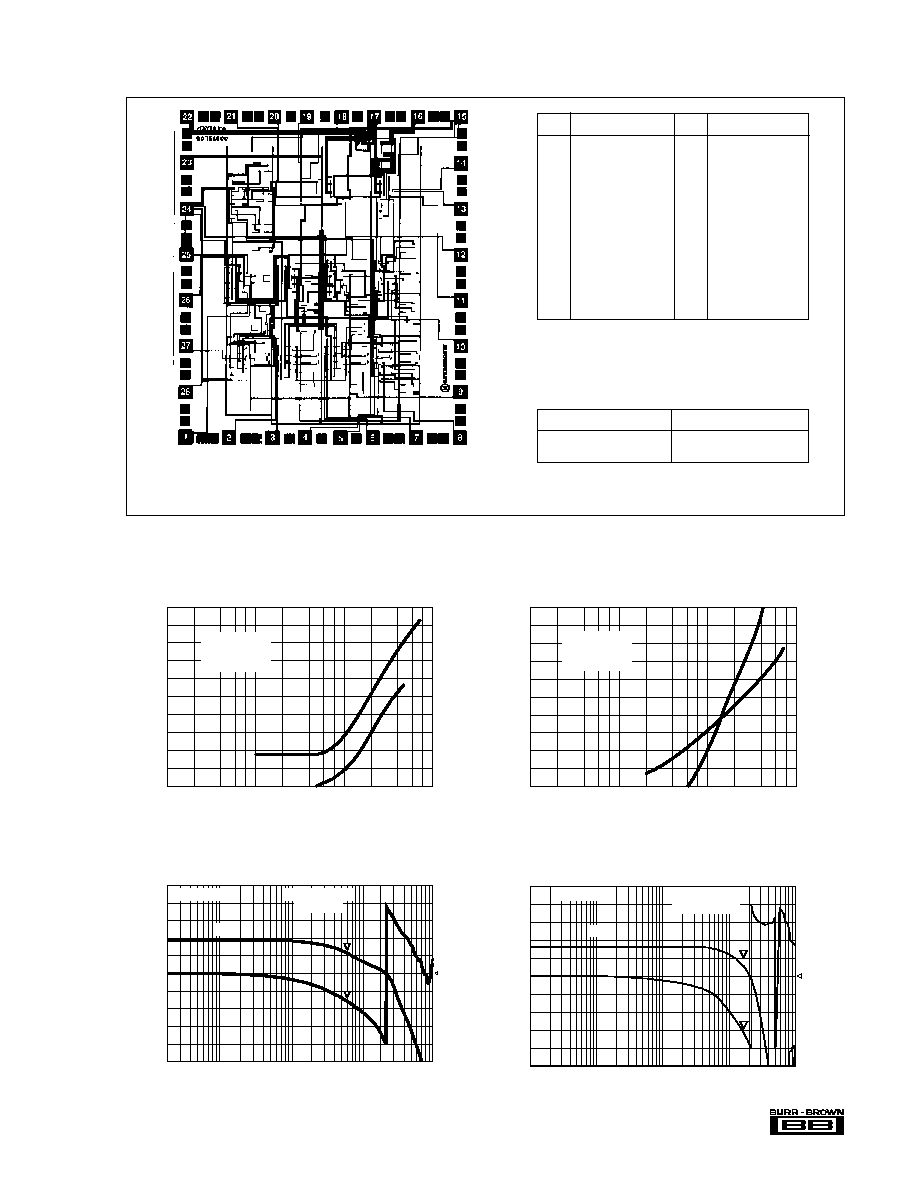
DICE INFORMATION
TYPICAL PERFORMANCE CURVES
PAD
FUNCTION
PAD
FUNCTION
1
TTL Set
15
+V
CC
2
≠In
B
16
+V
CC
3
+In
B
17
V
OUT
4
NC
18
NC
5
NC
19
NC
6
+In
A
20
NC
7
≠In
A
21
NC
8
NC
22
≠V
CC
9
V
OS
Adjust
23
≠V
CC
10
V
OS
Adjust
24
Ground
11
NC
25
CHA (TTL)
12
Comp Cap
26
ECL
OUT
13
NC
27
CHA (ECL)
14
NC
28
CHA (ECL)
NC: No Connection (Do Not Connect). OPA675-Do not use
pads 1, 25, 26. OPA676-Connect pad 26 to pad 27. Connect pad
1 to pad 28.
Substrate Bias: ≠V
CC
MECHANICAL INFORMATION
MILS (0.001")
Die Size
103 x 90
±
5
Die Thickness
20
±
3
OPA675/676 DIE TOPOGRAPHY
A
V
= +10V/V CLOSED-LOOP
SMALL SIGNAL BANDWIDTH
Frequency (MHz)
Gain (dB)
30
27
24
21
18
15
12
9
6
3
0
0.3
1
10
100
1000
0
≠45
≠90
≠135
≠180
Phase (∞)
C
C
= 6.5pF
BW = 185MHz
= ≠139.5∞
Gain
≠30
≠40
≠50
≠60
≠70
≠80
0.1
3f
2f
Harmonic Distortion (dBC)
Frequency (MHz)
Gain = +10V/V
R = 1k
V = 2.5Vp-p
L
O
100
10
1
LARGE SIGNAL
HARMONIC DISTORTION vs FREQUENCY

Æ
OPA675/676
6
10
9
8
7
6
5
4
3
2
1
0
0.3
1
1000
Gain (dB)
Frequency (MHz)
10
100
0
≠45
≠90
≠135
≠180
Phase (∞)
C = 35pF
Gain
BW = 100.3MHz
= ≠62.5∞
C
A
V
= +2V/V CLOSED-LOOP
SMALL SIGNAL BANDWIDTH
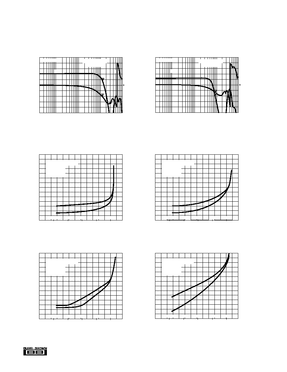
TYPICAL PERFORMANCE CURVES
(CONT)
20
18
16
14
12
10
8
6
4
2
0
0.3
1
1000
Gain (dB)
Frequency (MHz)
10
100
0
≠45
≠90
≠135
≠180
Phase (∞)
C
C
= 16pF
Gain
BW = 145.5MHz
= ≠99.6∞
A
V
= +5V/V CLOSED-LOOP
SMALL SIGNAL BANDWIDTH
≠20
≠30
≠40
≠50
≠60
≠70
≠80
≠90
≠20
≠15
0
+15
Distortion (dBC)
Power Output (dBm)
≠10
≠5
+5
+10
2f
3f
0.125Vp-p
0.25Vp-p
0.5Vp-p
1Vp-p
2Vp-p
A = +10V/V (20dB)
C = 6.5pF
R = 50
f = 1MHz
V
C
L
C
1MHz HARMONIC DISTORTION vs POWER OUTPUT
≠20
≠30
≠40
≠50
≠60
≠70
≠80
≠90
≠20
≠15
0
+15
Distortion (dBC)
Power Output (dBm)
≠10
≠5
+5
+10
2f
3f
0.125Vp-p
0.25Vp-p
0.5Vp-p
1Vp-p
2Vp-p
A = +10V/V (20dB)
C = 6.5pF
R = 50
f = 5MHz
V
C
L
C
5MHz HARMONIC DISTORTION vs POWER OUTPUT
≠20
≠30
≠40
≠50
≠60
≠70
≠80
≠90
≠20
≠15
0
+15
Distortion (dBC)
Power Output (dBm)
≠10
≠5
+5
+10
2f
3f
0.125Vp-p
0.25Vp-p
0.5Vp-p
1Vp-p
2Vp-p
A = +10V/V (20dB)
C = 6.5pF
R = 50
f = 10MHz
V
C
L
C
10MHz HARMONIC DISTORTION vs POWER OUTPUT
≠20
≠30
≠40
≠50
≠60
≠70
≠80
≠90
≠20
≠15
0
+15
Distortion (dBC)
Power Output (dBm)
≠10
≠5
+5
+10
2f
3f
V
C
L
C
20MHz HARMONIC DISTORTION vs POWER OUTPUT
A
V
= +10V/V (20dB)
C
C
= 6.5pF
R
L
= 50
f
C
= 20MHz
0.125Vp-p
0.25Vp-p
0.5Vp-p
1Vp-p
2Vp-p

Æ
OPA675/676
7
110
100
90
80
70
60
50
≠50
≠25
+50
+125
A ,PSR, and CMR (dB)
Temperature (∞C)
0
+25
+75
+100
CMR
PSR
A
OL
OL
OPEN-LOOP GAIN, CMR AND PSR vs TEMPERATURE
1
2
100
Compensation Capacitor (pF)
Noise Gain (V/V)
10
3
4 5 6
8
20
30
50
70
35
30
25
20
15
10
5
0
NOMINAL FREQUENCY COMPENSATION vs NOISE GAIN
0
≠15
≠30
≠45
≠60
≠75
≠90
≠105
≠120
0.3
1
1000
Crosstalk (dBC)
Frequency (MHz)
10
100
10.0MHz
≠68.3dB
CHANNEL-TO-CHANNEL
CROSSTALK vs FREQUENCY
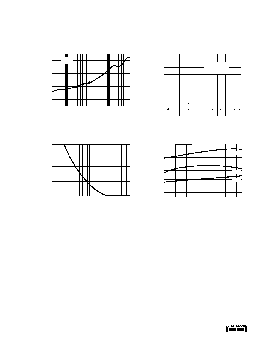
TYPICAL PERFORMANCE CURVES
(CONT)
THEORY OF OPERATION
An OPA675 simplified circuit is shown in Figure 1. It is a
"classical" high-speed op-amp architecture with one impor-
tant exception -- the amplifier has two ECL logic selectable
differential input stages. An appropriate differential ECL
logic signal on A and A (labeled B Select) will turn on either
Q5 or Q6, steering operating (tail) current to either differen-
tial input pair Q1 and Q2 or Q3 and Q4. The input pair
receiving the tail current operates as a conventional op-amp
input stage while the de-selected input pair receiving no tail
current appears as an open circuit. The de-selected inputs
have only a few pF parasitic capacitance and in the off
condition exhibit only a very low leakage (bias) current of
about 100pA. Two feedback networks can be connected to
each input separately allowing a wide range of circuit
applications. The feedback network connected to the se-
lected input operates in a normal op amp fashion while the
feedback network connected to the de-selected input is
totally inactive, appearing only as an additional load to the
amplifier's output stage.
The switched-input op amp (SWOP AMP)
circuit of the
OPA676 is basically the same as the OPA675 but a TTL
compatible level shifter (Figure 2) has been added to its input
selection logic circuit.
Standard TTL (OPA676) and ECL (OPA675) logic levels
may be applied to each input selection circuit but only
2
4
8
12
Frequency (MHz)
6
10
0
≠10
≠20
≠30
≠40
≠50
≠60
≠70
≠80
≠90
Output Power (dBm)
Gain = +10V/V
V
OUT
= 500mVp-p
R
L
= 50
2.5MHz SMALL-SIGNAL
HARMONIC DISTORTION SPECTRUM

Æ
OPA675/676
8
B
Select
A
Select
Q7
Q8
Q1
Q2
A
Q3
Q4
B
≠
+ ≠
+
Q5
Q6
+V
CC
Bias
Comp
I
TAIL
≠V
CC
Out
+V
CC
ECL
Out
TTL
In
ECL
Threshold
FIGURE 1. OPA675 Simplified Circuit Diagram.
FPO
FIGURE 3. 1% Settling Time.
FIGURE 2. Internal OPA676 TTL Logic Level Shifter.
FPO
350mV is typically required to switch between inputs. This
logic input sensitivity allows simpler high-speed logic driver
circuitry and it minimizes digital noise coupling into adja-
cent wideband analog circuitry and allows single ended ECL
inputs to be used with V
BB
applied to the other input.
The OPA675 and OPA676 are designed to be frequency
compensated by a single capacitor connected from pin 5 to
ground. Recommended compensation is shown in
Typical
Performance Curves. A small variable capacitor may be
trimmed for best bandwidth, settling time, and gain peaking.
This amplifier is designed for optimum performance in gains
of 5V/V to 20V/V, but it can also be used over a far wider
range of gains with excellent results. Closed-loop gain/phase
(Bode) plots are shown in the Typical Performance Curves.
OFFSET TRIM
Input offset voltage is low enough for many video applica-
tions. If desired, offset voltage can be trimmed with a 1k
potentiometer connected to +V
CC
. Trimming offset voltage
in this manner will effect both input A and input B;
independent control of input offset will require that trim
adjust current be summed into one or both inputs. This
technique is shown in a few applications circuits on the pages
to follow.

Æ
OPA675/676
9
500
100
100
5-30pf
75
2
1
5
8
+
≠
≠
+
500
50
To Scope
1MHz
Square
Wave
+0.5V
≠0.5V
100
1k
6.5pf
10MHz
50mVp-p
2
1
5
8
OPA676
+
≠
≠
+
16
15
11
100
1k
3MHz
TTL
100
R
L
12
Tektronix
SG503
To Scope
FIGURE 5. OPA676 Input Selection Transition Time Test
Circuit.
FIGURE 4. OPA675/676 Settling Time Test Circuit.
6.
Wirewound resistors (even "non-inductive" types) are
absolutely unacceptable in high frequency circuits.
7.
Avoid overloading the output. Remember that output
current must be provided by the amplifier to drive its
own feedback network as well as to drive its "load."
Lowest distortion is achieved with high impedance
loads.
8.
PC board traces for signal and power lines should be
wide to reduce impedance or inductance.
9.
Don't forget that these amplifiers use
±
5V supplies.
Although they will operate perfectly well with +5V
and ≠5.2V, the use of
±
15V supplies will result in
destruction.
10. Standard commercial test equipment has not been de-
signed to test devices in the OPA675/676 speed range.
Benchtop op amp testers and ATE systems will require
a special test head to successfully test these amplifiers.
11. High-speed amplifiers can drive only a limited amount
of capacitance. If the load exceeds 10 to 20pF consider
using a fast buffer or a small resistor to isolate the
capacitance from the amplifier's output. Capacitive
loads will cause loop instability if not compensated for.
12. Terminate transmission line loads. Unterminated lines,
such as coaxial cable, can appear to the amplifier to be
a capacitive or inductive load. By terminating a trans-
mission line with its characteristic impedance, the
amplifier's load then appears as a purely resistive
impedance.
13. For clean, fast input selection the logic input pins should
be terminated with appropriate resistors. Resistors should
be connected from input selection pins to ground plane
with short leads. Failure to terminate long lines will
result in ringing and poor high frequency switching.
14. Plug-in prototype boards and wire-wrap boards will not
be satisfactory. A clean layout using RF techniques is
required; there is no shortcut.
APPLICATION TIPS
Wideband amplifier circuits require good layout techniques
to be successful. The use of short, direct signal paths and
heavy (2 oz. copper recommended) ground planes are abso-
lutely necessary to achieve the performance level inherent in
the OPA675/676. Oscillation, ringing, poor bandwidth and
settling, gain peaking, and instability are typical problems
that plague all high-speed amplifiers when they are used in
poor layouts. The OPA675 and OPA676 are no different in
this respect--any amplifier with a gain bandwidth product of
a few GHz requires some care be taken in its application.
Points to remember:
1.
Use a heavy copper ground plane on the component side
of your PC board. This provides a low inductance
ground and it also conducts heat from active circuit
package pins into ambient air by convection.
2.
Bypass power supply pins directly at the active device.
The use of tantalum capacitors (1 to 10
µ
F/10V) with
very short leads is highly recommended. Supply pins
should not be left unbypassed.
3.
Signal paths should be short and direct. Feedback
resistors, compensation capacitors, termination resis-
tors, etc., should have lead lengths no longer than 1/4
inch (6cm).
4.
Surface-mount components (chip resistors, capacitors,
etc.) have low inductance and are therefore recom-
mended. Parasitic inductance and capacitance should be
avoided if best performance is to be achieved.
5.
Resistors used in feedback networks should have values
of a few hundred ohms for best performance. Shunt
capacitance problems limit the acceptable range to about
1k
or on the high resistance end and to a value that is
within the amplifier's output drive limits on the low end.
Metal film and carbon compensation resistors will be
satisfactory.

Æ
OPA675/676
10
1MHz TTL CARRIER FEEDTHROUGH vs FREQUENCY
0
2
6
10
Frequency (MHz)
4
8
+10
0
≠10
≠20
≠30
≠40
≠50
≠60
≠70
≠80
Carrier Feedthrough (dBm)
16
2
8
OPA676
316
1
15
A
B
12
5
12pF
≠
+
+
≠
4
49.9
50
Output
1k
+5V
Offset
Trim
49.9
50
Input
10
11
+
2.2µF
10V*
≠5V
* Tantalum
+
2.2µF
10V*
7
3
100
1k
6.5pF
10MHz
50mVp-p
2
3
5
8
OPA675
+
≠
≠
+
To Scope
3MHz
ECL
16
15
11
100
1k
≠5.2V
300
300
50
4
5
12
13
2
3
MC10105
16
2
11
8
5-30pF
OPA676
499
10k
1
499
15
A
B
5
≠
+
+
≠
Oscilloscope
or
Spectrum
Analyzer
To 50
50
49.9
49.9
49.9
40.2
Offset Trim
≠5V
+5V
5k
10
+2.8V
+0.4V
Input:
TTL rise and fall time = 10ns
Frequency = 1MHz
12
TTL
1
FIGURE 6. OPA675 Input Selection Transition Time Test Circuit.
FIGURE 9. Carrier Feedthrough from 1MHz TTL Logic.
Offset Trimmed for Maximum Carrier Rejec-
tion
FIGURE 7. OPA676 Carrier Feedthrough and Switching
Transient Test Circuit.
FIGURE 8. OPA676 Switching Transient. Top Trace: TTL
Input (2V/cm). Bottom Trace: Amplifier Output
(2mV/cm). Input B Offset Voltage has been
Trimmed to Match Input A Offset Voltage.
FIGURE 10. OPA676 Used as a Conventional Op Amp: A
10dB Gain Wideband Video Amplifier with
50
Input/Output Impedance.

Æ
OPA675/676
11
16
2
8
OPA676
301
20
1
15
A
B
11
5
3pF
≠
+
+
≠
12
Output
TTL
301
20
301
Input
3
4
+5V
1k
20
Bandwidth = ~200MHz
Input
49.9
12
16
2
7
4.7µF*
+
8
45
46
* Tantalum
ADC603
Signal
Input
Analog
Common
+5V
OPA676
10k
Offset Trim
100
100
1
412
59
15
A
B
4.7µF*
+
-5V
10
5
11
Gain Select (TTL)
3
4
39 pF
≠
+
+
≠
16
3
6
OPA675
1k
100
1
15
A
B
11
5
~5pF
≠
+
+
≠
TTL
12
100
OPA621
+
≠
Out
OPA621
+
≠
1k
200
200
200
Differential
Input
2
OPA621
+
≠
OPA621
+
≠
200
200
200
Differential
Input
1
1k
100
1k
2
3
6
2
2
6
3
2
6
3
100
2
8
OPA676
FIGURE 12. Programmable-Gain +2V/V (6dB) or +8V/V
(18dB) Buffer Amplifier for Floating-Point
Conversion.
FIGURE 13. High Input Impedance Differential Input Multiplexer with Gain of 30V/V (30dB).
FIGURE 11. Very Fast Programmable Gain Amplifier with
Voltage Gains of +1V/V and +16V/V (0dB and
24dB).

Æ
OPA675/676
12
Input
A
49.9
12
16
2
7
4.7µF*
+
8
45
46
* Tantalum
ADC603
Signal
Input
Analog
Common
+5V
OPA676
10k
Offset Trim
383
383
51.1
1
383
383
51.1
Input
B
15
A
B
4.7µF*
+
≠5V
10
5
11
Input Select (TTL)
3
4
4.7 pF
49.9
≠
+
+
≠
200
40
In
200
95.3
Out
100
16pF
10
Gain
Trim
10k
+5v
≠5v
40
10k
2
1
16
15
5
8
TTL
12
11
OPA676
+
≠
≠
+
Offset Trim
16
2
8
OPA676
909
90.9
1
15
A
B
11
5
6.5pF
≠
+
+
≠
12
49.9
50
RF or IF
Out
10
5k
4.99k
+5V
≠5V
49.9
TTL In
Noise
Blanking
Pulse
Input
909
100
49.9
49.9
50
RF or IF
In
16
2
8
OPA676
1k
100
1
15
A
B
11
5
~5pF
≠
+
+
≠
Output
1k
1k
In 1
100
13
Diff ECL
12
In 2
100
100
1k
+
≠
+
≠
A
A
R
2
R
1
In
C
R
2
R
1
Out
C
2
1
16
15
5
8
OPA676
TTL
12
11
+
≠
≠
+
OPA675
FIGURE 15. Multiplexed Input +16V/V Gain (24dB) Buffer
Amplifier.
FIGURE 14. Synchronous Modulator/Demodulator with Car-
rier Balance Trim (Gain =
±
5V/V).
FIGURE 16. Receiver Noise Blanker: A Wideband Gated
Video Amplifier.
FIGURE 17. Differential Input Multiplexer with Gain of
10V/V (20dB).
VOLTAGE GAIN
R
1
R
2
C
C
(V/V)
(
)
(
)
(pF)
+2
200
200
35
+5
49.9
200
16
+10
22.1
200
6.5
FIGURE 18. Programmable-Gain Amplifier.

Æ
OPA675/676
13
R
2
R
1
2
1
16
15
5
8
Out
In
R
3
C
C
R
4
TTL
12
11
OPA676
+
≠
≠
+
16
2
8
OPA675
909
90.2
1
15
A
B
11
5
6.5pF
≠
+
+
≠
13
1.5k
10
5k
4.99k
+5V
Diff ECL
909
≠5V
12
100
1k
OPA620
+
≠
1k
300Hz
to 3kHz
Audio
Input
A
A
455kHz
Carrier
Input
49.9
455kHz
BP
Filter*
OPA620
+
≠
1.5k
1k
1k
50
RF
Out
* Murata Erie
CFS455C
(Carrier Suppression)
Offset Trim
R
2
R
1
R
2
R
1
In 1
In 2
C
Out
C
2
1
16
15
5
8
TTL
12
11
OPA676
+
≠
≠
+
VOLTAGE GAIN
R
1
R
2
R
3
R
4
C
C
(V/V)
(
)
(
)
(
)
(
)
(pF)
±
2
100
200
200
200
35
±
5
40
200
50
200
16
±
10
20
200
25
225
6.5
FIGURE 21. Synchronous Modulator/Demodulator (with gain).
FIGURE 19. Single Sideband Suppressed Carrier Generator.
VOLTAGE GAIN
R
1
R
2
C
C
(V/V)
(
)
(
)
(pF)
+2
200
200
35
+4
75
226
22
+8
28
196
10
+16
20
301
3
+32
10
309
0
FIGURE 20. Two-Input Multiplexer (with gain).
