1
Æ
OPA689
©
1997 Burr-Brown Corporation
PDS-1409D
Printed in U.S.A. January, 2000
OPA689
Æ
Wideband, High Gain
VOLTAGE LIMITING AMPLIFIER
FEATURES
q
HIGH LINEARITY NEAR LIMITING
q
FAST RECOVERY FROM OVERDRIVE: 2.4ns
q
LIMITING VOLTAGE ACCURACY:
±
15mV
q
≠3dB BANDWIDTH (G = +6): 280MHz
q
STABLE FOR G
+4
q
SLEW RATE: 1600V/
µ
s
q
±
5V AND +5V SUPPLY OPERATION
q
LOW GAIN VERSION: OPA688
OPA689
OPA689
APPLICATIONS
q
TRANSIMPEDANCE WITH FAST
OVERDRIVE RECOVERY
q
FAST LIMITING ADC INPUT DRIVER
q
LOW PROP DELAY COMPARATOR
q
NON-LINEAR ANALOG SIGNAL
PROCESSING
q
DIFFERENCE AMPLIFIER
q
IF LIMITING AMPLIFIER
q
AM SIGNAL GENERATION
DESCRIPTION
The OPA689 is a wideband, voltage feedback op amp
that offers bipolar output voltage limiting, and is stable
for gains
+4. Two buffered limiting voltages take
control of the output when it attempts to drive beyond
these limits. This new output limiting architecture holds
the limiter offset error to
±
15mV. The op amp operates
linearly to within 30mV of the limits.
The combination of narrow nonlinear range and low
limiting offset allows the limiting voltages to be set within
100mV of the desired linear output range. A fast 2.4ns
recovery from limiting ensures that overdrive signals will
be transparent to the signal channel. Implementing the
limiting function at the output, as opposed to the input,
gives the specified limiting accuracy for any gain, and
allows the OPA689 to be used in all standard op amp
applications.
Non-linear analog signal processing circuits will benefit
from the OPA689's sharp transition from linear operation
to output limiting. The quick recovery time supports high
speed applications.
The OPA689 is available in an industry-standard pinout
in PDIP-8 and SO-8 packages. For lower gain applica-
tions requiring output limiting with fast recovery, con-
sider the OPA688.
2.5
2.0
1.5
1.0
0.5
0
≠0.5
≠1.0
≠1.5
≠2.0
≠2.5
LIMITED OUTPUT RESPONSE
V
IN
V
O
Time (200ns/div)
Input and Output Voltage (V)
G = +6
V
H
= 2.0V
V
L
= ≠2.0V
2.10
2.05
2.00
1.95
1.90
1.85
1.80
1.75
1.70
1.65
1.60
DETAIL OF LIMITED OUTPUT VOLTAGE
Time (50ns/div)
V
O
Input and Output Voltage (V)
International Airport Industrial Park ∑ Mailing Address: PO Box 11400, Tucson, AZ 85734 ∑ Street Address: 6730 S. Tucson Blvd., Tucson, AZ 85706 ∑ Tel: (520) 746-1111
Twx: 910-952-1111 ∑ Internet: http://www.burr-brown.com/ ∑ Cable: BBRCORP ∑ Telex: 066-6491 ∑ FAX: (520) 889-1510 ∑ Immediate Product Info: (800) 548-6132
For most current data sheet and other product
information, visit www.burr-brown.com
SBOS076
2
Æ
OPA689
AC PERFORMANCE (see Fig. 1)
Small Signal Bandwidth
V
O
< 0.5Vp-p
G = +6
280
220
210
200
MHz
Min
B
G = +12
90
--
--
--
MHz
Typ
C
G = ≠6
220
--
--
--
MHz
Typ
C
Gain Bandwidth Product (G
+20)
V
O
< 0.5Vp-p
720
490
460
430
MHz
Min
B
Gain Peaking
V
O
< 0.5Vp-p, G = +4
8
--
--
--
dB
Typ
C
0.1dB Gain Flatness Bandwidth
V
O
< 0.5Vp-p
110
--
--
--
MHz
Typ
C
Large Signal Bandwidth
V
O
= 2Vp-p
290
185
175
170
MHz
Min
B
Step Response
Slew Rate
2V Step
1600
1300
1250
950
V/
µ
s
Min
B
Rise/Fall Time
0.5V Step
1.2
1.8
1.9
2.4
ns
Max
B
Settling Time: 0.05%
2V Step
7
--
--
--
ns
Typ
C
Spurious Free Dynamic Range
f = 5MHz, V
O
= 2Vp-p
61
57
53
48
dB
Min
B
Differential Gain
NTSC, PAL, R
L
= 500
0.02
--
--
--
%
Typ
C
Differential Phase
NTSC, PAL, R
L
= 500
0.01
--
--
--
∞
Typ
C
Input Noise Density
Voltage Noise
f
1MHz
4.6
5.3
6.0
6.1
nV/
Hz
Max
B
Current Noise
f
1MHz
2.0
2.5
2.9
3.6
pA/
Hz
Max
B
DC PERFORMANCE (V
CM
= 0V)
Open-Loop Voltage Gain (A
OL
)
V
O
=
±
0.5V
56
50
48
47
dB
Min
A
Input Offset Voltage
±
1
±
5
±
6
±
7
mV
Max
A
Average Drift
--
--
±
14
±
14
µ
V/
∞
C
Max
B
Input Bias Current
(3)
+8
±
12
±
13
±
20
µ
A
Max
A
Average Drift
--
--
≠60
≠90
nA/
∞
C
Max
B
Input Offset Current
±
0.3
±
2
±
3
±
4
µ
A
Max
A
Average Drift
--
--
±
10
±
10
nA/
∞
C
Max
B
INPUT
Common-Mode Rejection Ratio
Input Referred, V
CM
=
±
0.5V
60
53
52
50
dB
Min
A
Common-Mode Input Range
(4)
±
3.3
±
3.2
±
3.2
±
3.1
V
Min
A
Input Impedance
Differential-Mode
0.4 || 1
--
--
--
M
|| pF
Typ
C
Common-Mode
1 || 1
--
--
--
M
|| pF
Typ
C
OUTPUT
V
H
= ≠V
L
= 4.3V
Output Voltage Range
R
L
500
±
4.1
±
3.9
±
3.9
±
3.8
V
Min
A
Current Output, Sourcing
105
90
85
80
mA
Min
A
Sinking
≠85
≠70
≠65
≠60
mA
Min
A
Closed-Loop Output Impedance
G = +4, f < 100kHz
0.8
--
--
--
Typ
C
POWER SUPPLY
Operating Voltage, Specified
±
5
--
--
--
V
Typ
C
Maximum
--
±
6
±
6
±
6
V
Max
A
Quiescent Current, Maximum
15.8
17
19
20
mA
Max
A
Minimum
15.8
14
12.8
11
mA
Min
A
Power Supply Rejection Ratio
+V
S
= 4.5V to 5.5V
+PSR (Input Referred)
65
58
57
55
dB
Min
A
OUTPUT VOLTAGE LIMITERS
Default Limit Voltage
Limiter Pins Open
±
3.3
±
3.0
±
3.0
±
2.9
V
Min
A
Minimum Limiter Separation (V
H
≠ V
L
)
200
200
200
200
mV
Min
B
Maximum Limit Voltage
--
±
4.3
±
4.3
±
4.3
V
Max
B
Limiter Input Bias Current Magnitude
(5)
V
O
= 0
Maximum
54
65
68
70
µ
A
Max
A
Minimum
54
35
34
31
µ
A
Min
A
Average Drift
--
--
40
45
nA/
∞
C
Max
B
Limiter Input Impedance
2 || 1
--
--
--
M
|| pF
Typ
C
Limiter Feedthrough
(6)
f = 5MHz
≠60
--
--
--
dB
Typ
C
DC Performance in Limit Mode
V
IN
=
±
0.7V
Limiter Offset Voltage
(V
O
≠ V
H
) or (V
O
≠ V
L
)
±
15
±
35
±
40
±
40
mV
Max
A
Op Amp Input Bias Current Shift
(3)
3
--
--
--
µ
A
Typ
C
OPA689U, P
TYP
GUARANTEED
(1)
0
∞
C to
≠40
∞
C to
MIN/
TEST
PARAMETER
CONDITIONS
+25
∞
C
+25
∞
C
+70
∞
C
+85
∞
C
UNITS
MAX LEVEL
(2)
SPECIFICATIONS -- V
S
=
±
5V
G = +6, R
L
= 500
, R
F
= 750
,
V
H
= ≠V
L
= 2V, (Figure 1 for AC performance only), unless otherwise noted.

3
Æ
OPA689
OUTPUT VOLTAGE LIMITERS (CONT)
AC Performance in Limit Mode
Limiter Small Signal Bandwidth
V
IN
=
±
0.7V, V
O
< 0.02Vp-p
450
--
--
--
MHz
Typ
C
Limiter Slew Rate
(7)
100
--
--
--
V/
µ
s
Typ
C
Limited Step Response
Overshoot
V
IN
= 0 to
±
0.7V Step
250
--
--
--
mV
Typ
C
Recovery Time
V
IN
=
±
0.7V to 0 Step
2.4
2.8
3.0
3.2
ns
Max
B
Linearity Guardband
(8)
f = 5MHz, V
O
= 2Vp-p
30
--
--
--
mV
Typ
C
THERMAL CHARACTERISTICS
Temperature Range
Specification: P, U
≠40 to +85
--
--
--
∞
C
Typ
C
Thermal Resistance
P
8-Pin DIP
100
--
--
--
∞
C/W
Typ
C
U
8-Pin SO-8
125
--
--
--
∞
C/W
Typ
C
NOTES: (1) Junction Temperature = Ambient Temperature for low temperature limit and 25
∞
C guaranteed specifications. Junction Temperature = Ambient Temperature
+ 23
∞
C at high temperature limit guaranteed specifications. (2) TEST LEVELS: (A) 100% tested at 25
∞
C. Over temperature limits by characterization and simulation.
(B) Limits set by characterization and simulation. (C) Typical value for information only. (3) Current is considered positive out of node. (4) CMIR tested as < 3dB
degradation from minimum CMRR at specified limits. (5) I
VH
(V
H
bias current) is positive, and I
VL
(V
L
bias current) is negative, under these conditions. See Note 3 and
Figures 1 and 7. (6) Limiter feedthrough is the ratio of the output magnitude to the sinewave added to V
H
(or V
L
) when V
IN
= 0. (7) V
H
slew rate conditions are: V
IN
= +0.7V, G = +6, V
L
= ≠2V, V
H
= step between 2V and 0V. V
L
slew rate conditions are similar. (8) Linearity Guardband is defined for an output sinusoid (f = 1MHz,
V
O
= 2Vpp) centered between the limiter levels (V
H
and V
L
). It is the difference between the limiter level and the peak output voltage where SFDR decreases by 3dB
(see Figure 8).
OPA689U, P
TYP
GUARANTEED
(1)
0
∞
C to
≠40
∞
C to
MIN/
TEST
PARAMETER
CONDITIONS
+25
∞
C
+25
∞
C
+70
∞
C
+85
∞
C
UNITS
MAX LEVEL
(2)
SPECIFICATIONS -- V
S
=
±
5V
(cont.)
G = +6, R
L
= 500
, R
F
= 750
,
V
H
= ≠V
L
= 2V, (Figure 1 for AC performance only), unless otherwise noted.
The information provided herein is believed to be reliable; however, BURR-BROWN assumes no responsibility for inaccuracies or omissions. BURR-BROWN assumes
no responsibility for the use of this information, and all use of such information shall be entirely at the user's own risk. Prices and specifications are subject to change
without notice. No patent rights or licenses to any of the circuits described herein are implied or granted to any third party. BURR-BROWN does not authorize or warrant
any BURR-BROWN product for use in life support devices and/or systems.
4
Æ
OPA689
AC PERFORMANCE (see Fig. 2)
Small Signal Bandwidth
V
O
< 0.5Vp-p
G = +6
210
180
160
150
MHz
Min
B
G = +12
70
--
--
--
MHz
Typ
C
G = ≠6
180
--
--
--
MHz
Typ
C
Gain Bandwidth Product (G
+20)
V
O
< 0.5Vp-p
440
330
310
300
MHz
Min
B
Gain Peaking
V
O
< 0.5Vp-p, G = +4
4
--
--
--
dB
Typ
B
0.1dB Gain Flatness Bandwidth
V
O
< 0.5Vp-p
35
--
--
--
MHz
Typ
C
Large Signal Bandwidth
V
O
= 2Vp-p
175
150
140
125
MHz
Min
B
Step Response
Slew Rate
2V Step
1600
1300
1250
950
V/
µ
s
Min
B
Rise/Fall Time
0.5V Step
1.9
2.1
2.2
2.6
ns
Max
B
Settling Time: 0.05%
2V Step
7
--
--
--
ns
Typ
C
Spurious Free Dynamic Range
f = 5MHz, V
O
= 2Vp-p
59
55
51
46
dB
Min
B
Input Noise
Voltage Noise Density
f
1MHz
4.6
5.3
6.0
6.1
nV/
Hz
Max
B
Current Noise Density
f
1MHz
2.0
2.5
2.9
3.6
pA/
Hz
Max
B
DC PERFORMANCE
Open-Loop Voltage Gain (A
OL
)
V
O
=
±
0.5V
56
50
48
47
dB
Min
A
Input Offset Voltage
±
1
±
5
±
6
±
8
mV
Max
A
Average Drift
--
--
±
14
±
14
µ
V/
∞
C
Max
B
Input Bias Current
(3)
+8
±
12
±
13
±
20
µ
A
Max
A
Average Drift
--
--
≠60
≠90
nA/
∞
C
Max
B
Input Offset Current
±
0.3
±
2
±
3
±
4
µ
A
Max
A
Average Drift
--
--
±
10
±
10
nA/
∞
C
Max
B
INPUT
Common-Mode Rejection Ratio
Input Referred, V
CM
±
0.5V
58
51
50
48
dB
Min
A
Common-Mode Input Range
(4)
V
CM
±
0.8
V
CM
±
0.7
V
CM
±
0.7
V
CM
±
0.6
V
Min
A
Input Impedance
Differential-Mode
0.4 || 1
--
--
--
M
|| pF
Typ
C
Common-Mode
1 || 1
--
--
--
M
|| pF
Typ
C
OUTPUT
V
H
= V
CM
+ 1.8V, V
L
= V
CM
≠ 1.8V
Output Voltage Range
R
L
500
V
CM
±
1.6
V
CM
±
1.4
V
CM
±
1.4
V
CM
±
1.3
V
Min
A
Current Output, Sourcing
70
60
55
50
mA
Min
A
Sinking
≠60
≠50
≠45
≠40
mA
Min
A
Closed-Loop Output Impedance
G = +4, f < 100kHz
0.8
--
--
--
Typ
C
POWER SUPPLY
Operating Voltage, Specified
5
--
--
--
V
Typ
C
Maximum
--
12
12
12
V
Max
A
Quiescent Current, Maximum
13
15
15
16
mA
Max
A
Minimum
13
11
10
9
mA
Min
A
Power Supply Rejection Ratio
V
S
= 4.5V to 5.5V
+PSR (Input Referred)
65
--
--
--
dB
Typ
C
OUTPUT VOLTAGE LIMITERS
Default Limiter Voltage
Limiter Pins Open
V
CM
±
0.9
V
CM
±
0.6
V
CM
±
0.6
V
CM
±
0.6
V
Min
A
Minimum Limiter Separation (V
H
≠ V
L
)
200
200
200
200
mV
Min
B
Maximum Limit Voltage
--
V
CM
±
1.8
V
CM
±
1.8
V
CM
±
1.8
V
Max
B
Limiter Input Bias Current Magnitude
(5)
V
O
= 2.5V
Maximum
35
65
75
85
µ
A
Max
A
Minimum
35
0
0
0
µ
A
Min
A
Average Drift
--
--
30
50
nA/
∞
C
Max
B
Limiter Input Impedance
2 || 1
--
--
--
M
|| pF
Typ
C
Limiter Isolation
(6)
f = 5MHz
≠60
--
--
--
dB
Typ
C
DC Performance in Limit Mode
V
IN
= V
CM
±
0.4V
Limiter Voltage Accuracy
(V
O
≠ V
H
) or (V
O
≠ V
L
)
±
15
±
35
±
40
±
40
mV
Max
A
Op Amp Bias Current Shift
(3)
5
--
--
--
µ
A
Typ
C
AC Performance in Limit Mode
Limiter Small Signal Bandwidth
V
IN
=
±
0.4V, V
O
< 0.02Vp-p
300
--
--
--
MHz
Typ
C
Limiter Slew Rate
(7)
20
--
--
--
V/
µ
s
Typ
C
Limited Step Response
Overshoot
V
IN
= V
CM
to V
CM
±
0.4V Step
55
--
--
--
mV
Typ
C
Recovery Time
V
IN
= V
CM
±
0.4V to V
CM
Step
15
--
--
--
ns
Typ
C
Linearity Guardband
(8)
f = 5MHz, V
O
= 2Vp-p
30
--
--
--
mV
Typ
C
OPA689U, P
TYP
GUARANTEED
(1)
0
∞
C to
≠40
∞
C to
MIN/
TEST
PARAMETER
CONDITIONS
+25
∞
C
+25
∞
C
+70
∞
C
+85
∞
C
UNITS
MAX LEVEL
(2)
SPECIFICATIONS -- V
S
= +5V
G = +6, R
F
= 750
,
R
L
= 500
tied to V
CM
= 2.5V, V
L
= V
CM
≠1.2V, V
H
= V
CM
+1.2V, (Figure 2 for AC performance only), unless otherwise noted.
5
Æ
OPA689
THERMAL CHARACTERISTICS
Temperature Range
Specification: P, U
≠40 to +85
--
--
--
∞
C
Typ
C
Thermal Resistance
P
8-Pin DIP
100
--
--
--
∞
C/W
Typ
C
U
8-Pin SO-8
125
--
--
--
∞
C/W
Typ
C
NOTES: (1) Junction Temperature = Ambient Temperature for low temperature limit and 25
∞
C guaranteed specifications. Junction Temperature = Ambient Temperature
+ 23
∞
C at high temperature limit guaranteed specifications. (2) TEST LEVELS: (A) 100% tested at 25
∞
C. Over temperature limits by characterization and simulation.
(B) Limits set by characterization and simulation. (C) Typical value for information only. (3) Current is considered positive out of node. (4) CMIR tested as < 3dB
degradation from minimum CMRR at specified limits. (5) I
VH
(V
H
bias current) is negative, and I
VL
(V
L
bias current) is positive, under these conditions. See Note 3 and
Figures 2 and 7. (6) Limiter feedthrough is the ratio of the output magnitude to the sinewave added to V
H
(or V
L
) when V
IN
= 0. (7) V
H
slew rate conditions are: V
IN
= V
CM
+0.4V, G = +6, V
L
= V
CM
≠1.2V, V
H
= step between V
CM
+1.2V and V
CM
. V
L
slew rate conditions are similar. (8) Linearity Guardband is defined for an output
sinusoid (f = 5MHz, V
O
= V
CM
±
1Vp-p) centered between the limiter levels (V
H
and V
L
). It is the difference between the limiter level and the peak output voltage where
SFDR decreases by 3dB (see Figure 8).
OPA689U, P
TYP
GUARANTEED
(1)
0
∞
C to
≠40
∞
C to
MIN/
TEST
PARAMETER
CONDITIONS
+25
∞
C
+25
∞
C
+70
∞
C
+85
∞
C
UNITS
MAX LEVEL
(2)
SPECIFICATIONS -- V
S
= +5V
(cont.)
G = +6, R
F
= 750
,
R
L
= 500
tied to V
CM
= 2.5V, V
L
= V
CM
≠1.2V, V
H
= V
CM
+1.2V, (Figure 2 for AC performance only), unless otherwise noted.
ELECTROSTATIC
DISCHARGE SENSITIVITY
This integrated circuit can be damaged by ESD. Burr-Brown
recommends that all integrated circuits be handled with
appropriate precautions. Failure to observe proper handling
and installation procedures can cause damage.
ESD damage can range from subtle performance degradation
to complete device failure. Precision integrated circuits may
be more susceptible to damage because very small parametric
changes could cause the device not to meet its published
specifications.
Supply Voltage .................................................................................
±
6.5V
Internal Power Dissipation ........................... See Thermal Characteristics
Input Voltage Range ............................................................................
±
V
S
Differential Input Voltage .....................................................................
±
V
S
Limiter Voltage Range ...........................................................
±
(V
S
≠ 0.7V)
Storage Temperature Range: P, U ................................ ≠40
∞
C to +125
∞
C
Lead Temperature (DIP, soldering, 10s) ...................................... +300
∞
C
(SO-8, soldering, 3s) ...................................... +260
∞
C
Junction Temperature .................................................................... +175
∞
C
ABSOLUTE MAXIMUM RATINGS
ABSOLUTE MAXIMUM RATINGS
Top View
DIP-8, SO-8
1
2
3
4
8
7
6
5
NC
Inverting Input
Non-Inverting Input
≠V
S
V
H
+V
S
Output
V
L
PACKAGE/ORDERING INFORMATION
PACKAGE
SPECIFIED
DRAWING
TEMPERATURE
PACKAGE
ORDERING
TRANSPORT
PRODUCT
PACKAGE
NUMBER
RANGE
MARKING
NUMBER
(1)
MEDIA
OPA689P
DIP-8
006
≠40
∞
C to +85
∞
C
OPA689P
OPA689P
Rails
OPA689U
SO-8 Surface Mount
182
≠40
∞
C to +85
∞
C
OPA689U
OPA689U
Rails
"
"
"
"
"
OPA689U/2K5
Tape and Reel
NOTES: (1) Models with a slash (/ ) are available only in Tape and Reel in the quantities indicated (e.g., /2K5 indicates 2500 devices per reel). Ordering 2500 pieces
of "OPA689U/2K5" will get a single 2500-piece Tape and Reel.
6
Æ
OPA689
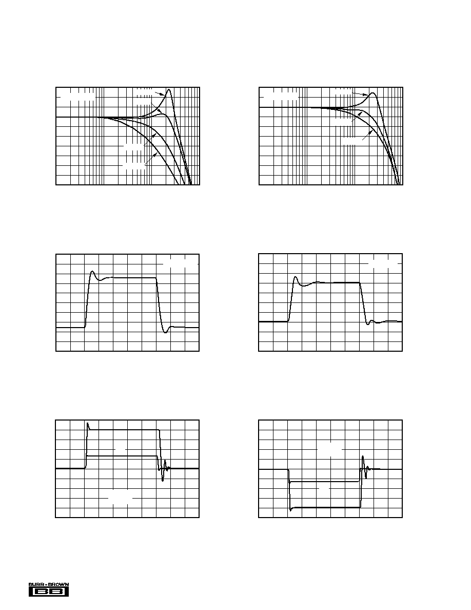
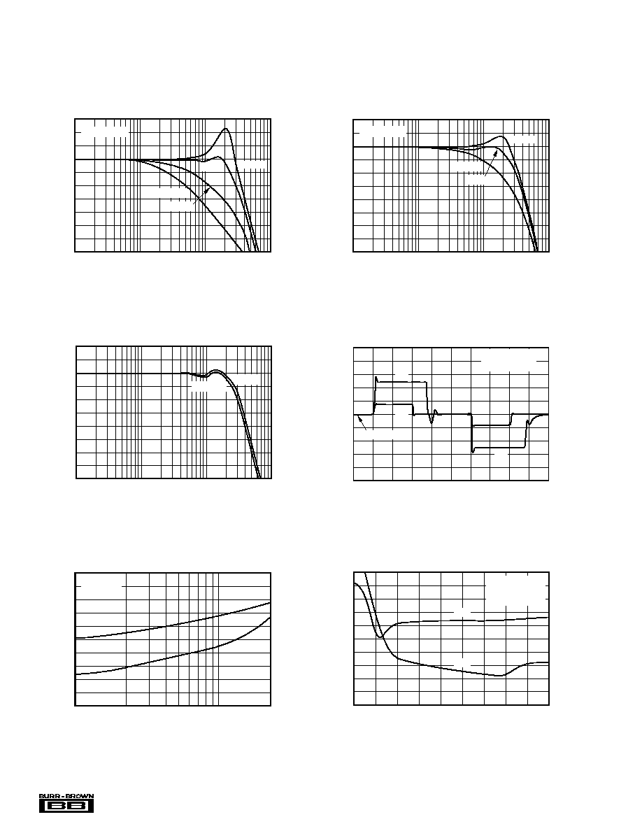
TYPICAL PERFORMANCE CURVES-- V
S
=
±
5V
G = +6, R
L
= 500
, R
F
= 750
,
V
H
= ≠V
L
= 2V, (Figure 1 for AC performance only), unless otherwise noted.
9
6
3
0
≠3
≠6
≠9
≠12
≠15
≠18
≠21
NON-INVERTING SMALL-SIGNAL
FREQUENCY RESPONSE
Frequency (Hz)
Normalized Gain (dB)
1M
10M
100M
1G
V
O
= 0.5Vp-p
G = +12
G = +20
G = +4
G = +6
6
3
0
≠3
≠6
≠9
≠12
≠15
≠18
≠21
≠24
INVERTING SMALL-SIGNAL
FREQUENCY RESPONSE
Frequency (Hz)
Normalized Gain (dB)
1M
10M
100M
1G
V
O
= 0.5Vp-p
G = ≠6
G = ≠12
G = ≠4
SMALL-SIGNAL PULSE RESPONSE
Time (5ns/div)
Output Voltage (V)
V
O
= 0.5Vp-p
0.5
0.4
0.3
0.2
0.1
0
≠0.1
≠0.2
≠0.3
≠0.4
≠0.5
LARGE-SIGNAL PULSE RESPONSE
Time (5ns/div)
V
O
= 2Vp-p
Output Voltage (V)
2.5
2.0
1.5
1.0
0.5
0
≠0.5
≠1.0
≠1.5
≠2.0
≠2.5
V
H
--LIMITED PULSE RESPONSE
V
O
2.5
2.0
1.5
1.0
0.5
0
≠0.5
≠1.0
≠1.5
≠2.0
≠2.5
Time (20ns/div)
Input and Output Voltages (V)
V
IN
V
H
= +2V
G = +6
V
L
--LIMITED PULSE RESPONSE
2.5
2.0
1.5
1.0
0.5
0
≠0.5
≠1.0
≠1.5
≠2.0
≠2.5
Time (20ns/div)
Input and Output Voltages (V)
V
O
V
IN
V
L
= ≠2V
G = +6
7
Æ
OPA689
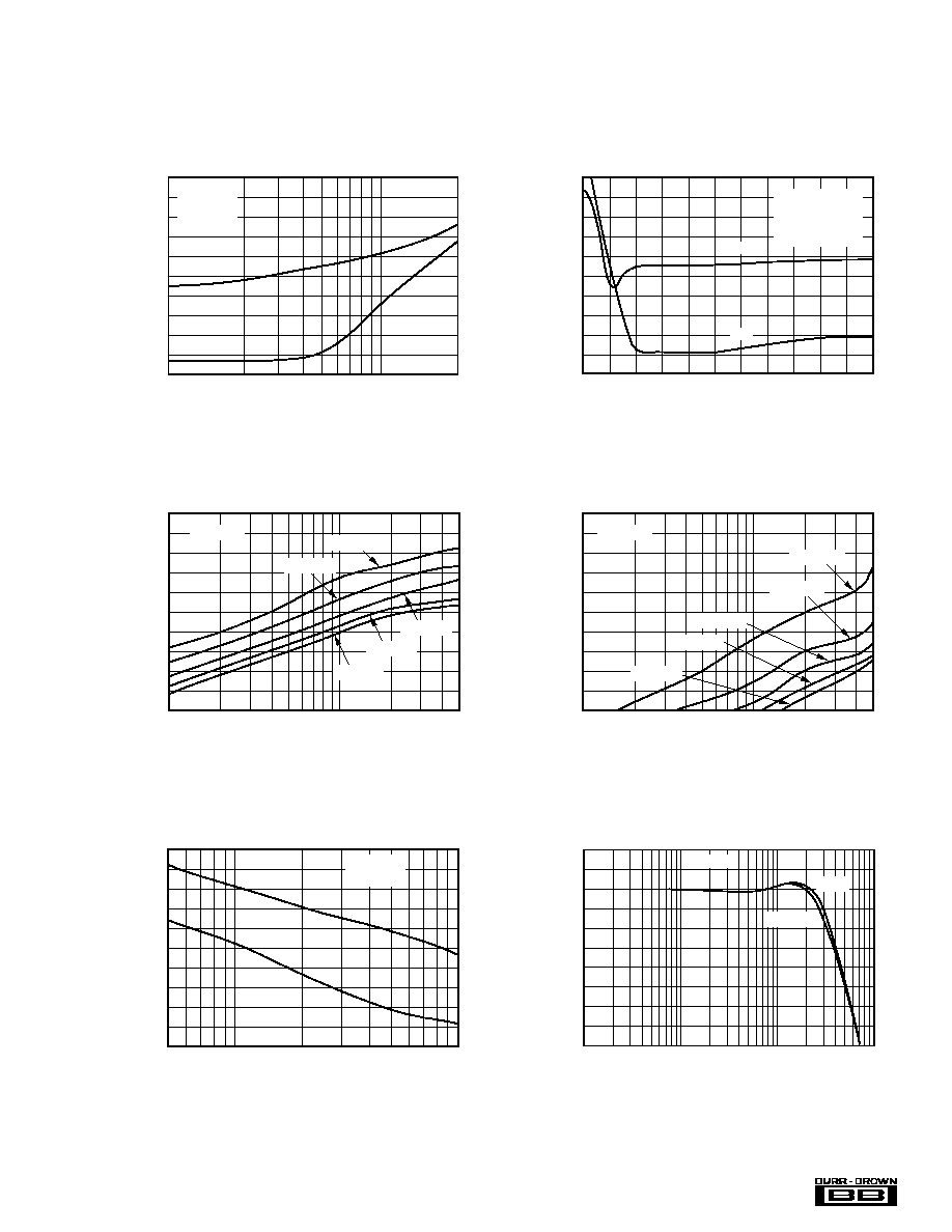
TYPICAL PERFORMANCE CURVES-- V
S
=
±
5V
(cont.)
G = +6, R
L
= 500
, R
F
= 750
,
V
H
= ≠V
L
= 2V, (Figure 1 for AC performance only), unless otherwise noted.
≠40
≠45
≠50
≠55
≠60
≠65
≠70
≠75
≠80
≠85
≠90
2ND HARMONIC DISTORTION vs OUTPUT SWING
Output Swing (Vp-p)
2nd Harmonic Distortion (dBc)
0.1
1.0
5.0
R
L
= 500
f
1
= 20MHz
f
1
= 10MHz
f
1
= 1MHz
f
1
= 5MHz
f
1
= 2MHz
≠40
≠45
≠50
≠55
≠60
≠65
≠70
≠75
≠80
≠85
≠90
3RD HARMONIC DISTORTION vs OUTPUT SWING
Output Swing (Vp-p)
3rd Harmonic Distortion (dBc)
0.1
1.0
5.0
R
L
= 500
f
1
= 20MHz
f
1
= 10MHz
f
1
= 5MHz
f
1
= 2MHz
f
1
= 1MHz
HARMONIC DISTORTION vs FREQUENCY
≠40
≠45
≠50
≠55
≠60
≠65
≠70
≠75
≠80
≠85
≠90
2nd and 3rd Harmonic Distortion (dBc)
HD2
HD3
V
O
= 2Vp-p
R
L
= 500
Frequency (Hz)
1M
10M
20M
≠40
≠45
≠50
≠55
≠60
≠65
≠70
≠75
≠80
≠85
≠90
HARMONIC DISTORTION vs LOAD RESISTANCE
Load Resistance (
)
2nd and 3rd Harmonic Distortion (dBc)
50
100
1000
V
O
= 2Vp-p
f
1
= 5MHz
HD2
HD3
21.6
18.6
15.6
12.6
9.6
6.6
3.6
0.6
≠2.4
≠5.4
≠8.4
LARGE SIGNAL FREQUENCY RESPONSE
Frequency (Hz)
0.1
10M
100M
1G
Gain (dB)
G = +6
0.5Vp-p
2Vp-p
HARMONIC DISTORTION NEAR LIMIT VOLTAGES
≠40
≠45
≠50
≠55
≠60
≠65
≠70
≠75
≠80
≠85
≠90
± Limit Voltage (V)
0.9
1.0
1.1
1.2
1.3
1.4
1.5
1.6
1.7
1.8
1.9
2.0
2nd and 3rd Harmonic Distortion (dBc)
V
O
= 0V
DC
±1Vp
f
1
= 5MHz
R
L
= 500
HD2
HD3
8
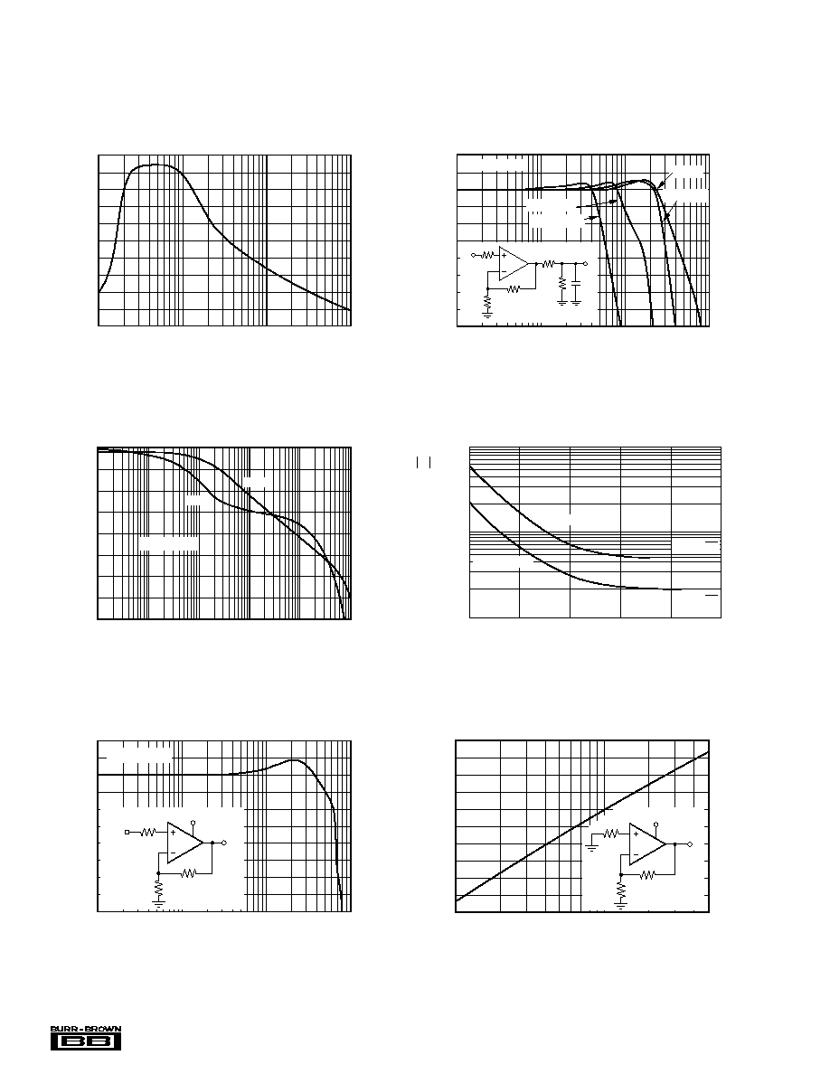
Æ
OPA689
TYPICAL PERFORMANCE CURVES-- V
S
=
±
5V
(cont.)
G = +6, R
L
= 500
, R
F
= 750
,
V
H
= ≠V
L
= 2V, (Figure 1 for AC performance only), unless otherwise noted.
100
10
1
INPUT NOISE DENSITY
Frequency (Hz)
100
1k
10k
100k
1M
10M
Input Voltage Noise Density (nV/
Hz)
Input Current Noise Density (pA/
Hz)
Voltage Noise
4.6nV/
Hz
Current Noise
2.0pA/
Hz
60
50
40
30
20
10
0
≠10
≠20
OPEN-LOOP FREQUENCY RESPONSE
Frequency (Hz)
10k
100k
1M
10M
100M
1G
Open-Loop Gain (dB)
0
≠30
≠60
≠90
≠120
≠150
≠180
≠210
≠240
Open-Loop Phase (deg)
Gain
Phase
V
O
= 0.5Vp-p
6
3
0
≠3
≠6
≠9
≠12
≠15
≠18
≠21
≠24
LIMITER SMALL-SIGNAL FREQUENCY RESPONSE
Frequency (Hz)
1M
10M
100M
1G
Limiter Gain (dB)
V
O
= 0.02Vp-p
750
125
150
V
O
8
V
H
= 0.02Vp-p + 2.0V
DC
0.7V
DC
≠30
≠35
≠40
≠45
≠50
≠55
≠60
≠65
≠70
≠75
≠80
LIMITER FEEDTHROUGH
Frequency (Hz)
Feedthrough (dB)
1M
10M
50M
750
125
150
V
O
8
V
H
= 0.02Vp-p + 2V
DC
21.6
18.6
15.6
12.6
9.6
6.6
3.6
0.6
≠2.4
≠5.4
≠8.4
FREQUENCY RESPONSE vs CAPACITIVE LOAD
Frequency (Hz)
0.1
10M
100M
1G
Gain to Capacitive Load (dB)
V
O
= 0.5Vp-p
C
L
= 100pF
C
L
= 0
C
L
= 1000pF
C
L
= 10pF
OPA689
R
S
125
V
IN
V
O
C
L
1k
1k
is optional
750
150
50
45
40
35
30
25
20
15
10
5
0
R
S
vs CAPACITIVE LOAD
Capacitive Load (pF)
1
10
100
1000
R
S
(
)
9
Æ
OPA689
TYPICAL PERFORMANCE CURVES-- V
S
=
±
5V
(cont.)
G = +6, R
L
= 500
, R
F
= 750
,
V
H
= ≠V
L
= 2V, (Figure 1 for AC performance only), unless otherwise noted.
100
10
1
0.1
CLOSED-LOOP OUTPUT IMPEDANCE
Frequency (Hz)
100k
1G
1M
10M
100M
Output Impedance (
)
G = +4
V
O
= 0.5Vp-p
20
18
16
14
12
10
SUPPLY AND OUTPUT CURRENTS vs TEMPERATURE
Ambient Temperature (∞C)
≠50
≠25
0
25
50
75
100
Supply Current (mA)
200
180
160
140
120
100
Output Current (mA)
Output Current, Sourcing
Supply Current
| Output Current, Sinking |
100
95
90
85
80
75
70
65
60
55
50
PSR AND CMR vs TEMPERATURE
Ambient Temperature (∞C)
≠50
≠25
0
25
50
75
100
PSR and CMR, Input Referred (dB)
PSR≠
PSRR
PSR+
CMRR
5.0
4.5
4.0
3.5
3.0
VOLTAGE RANGES vs TEMPERATURE
Ambient Temperature (∞C)
≠50
≠25
0
25
50
75
100
± Voltage Range (V)
Output Voltage Range
V
H
= ≠V
L
= 4.3V
Common-Mode Input Range
100
75
50
25
0
≠25
≠50
≠75
≠100
LIMITER INPUT BIAS CURRENT vs BIAS VOLTAGE
Limiter Headroom (V)
0.0
0.5
1.0
1.5
2.0
2.5
3.0
3.5
4.0
4.5
5.0
Limter Input Bias Current (
µ
A)
Maximum Over Temperature
Minimum Over Temperature
Limiter Headroom = +V
S
≠ V
H
Current = I
VH
or ≠I
VL
= V
L
≠ (≠V
S
)
10
Æ
OPA689
TYPICAL PERFORMANCE CURVES-- V
S
= +5V
G = +6, R
F
= 402
, R
L
= 500
tied to V
CM
= 2.5V
,
V
L
= V
CM
≠1.2V
,
V
H
= V
CM
+1.2V, (Figure 2 for AC performance only), unless otherwise noted.
9
6
3
0
≠3
≠6
≠9
≠12
≠15
≠18
≠21
NON-INVERTING SMALL-SIGNAL
FREQUENCY RESPONSE
Frequency (Hz)
Normalized Gain (dB)
1M
10M
100M
1G
V
O
= 0.5Vp-p
G = +12
G = +20
G = +4
G = +6
6
3
0
≠3
≠6
≠9
≠12
≠15
≠18
≠21
≠24
INVERTING SMALL-SIGNAL
FREQUENCY RESPONSE
Frequency (Hz)
Normalized Gain (dB)
1M
10M
100M
1G
V
O
= 0.5Vp-p
G = ≠6
G = ≠12
G = ≠4
21.6
18.6
15.6
12.6
9.6
6.6
3.6
0.6
≠2.4
≠5.4
≠8.4
LARGE-SIGNAL FREQUENCY RESPONSE
Frequency (Hz)
0.1
10M
100M
1G
Gain (dB)
0.5Vp-p
2Vp-p
≠40
≠45
≠50
≠55
≠60
≠65
≠70
≠75
≠80
≠85
≠90
HARMONIC DISTORTION vs FREQUENCY
Frequency (Hz)
1M
10M
20M
2nd and 3rd Harmonic Distortion (dBc)
V
O
= 2Vp-p
R
L
= 500
HD2
HD3
≠40
≠45
≠50
≠55
≠60
≠65
≠70
≠75
≠80
≠85
≠90
HARMONIC DISTORTION NEAR LIMIT VOLTAGES
| Limit Voltages ≠ 2.5V
DC
|
0.9
1.0
1.1
1.2
1.3
1.4
1.5
1.6
1.7
1.8
2nd and 3rd Harmonic Distortion (dBc)
V
O
= 2.5V
DC
±1Vp
f
1
= 5MHz
R
L
= 500
HD2
HD3
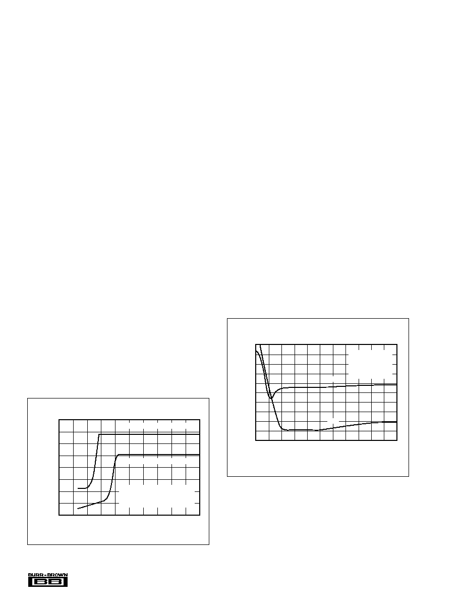
V
H
AND
V
H
--LIMITED PULSE RESPONSE
5.0
4.5
4.0
3.5
3.0
2.5
2.0
1.5
1.0
0.5
0
Time (20ns/div)
Input and Output Voltages (V)
V
H
= V
CM
+1.2V
V
L
= V
CM
≠1.2V
V
O
V
O
V
IN
V
IN
V
CM
= 2.5V
11
Æ
OPA689
TYPICAL APPLICATIONS
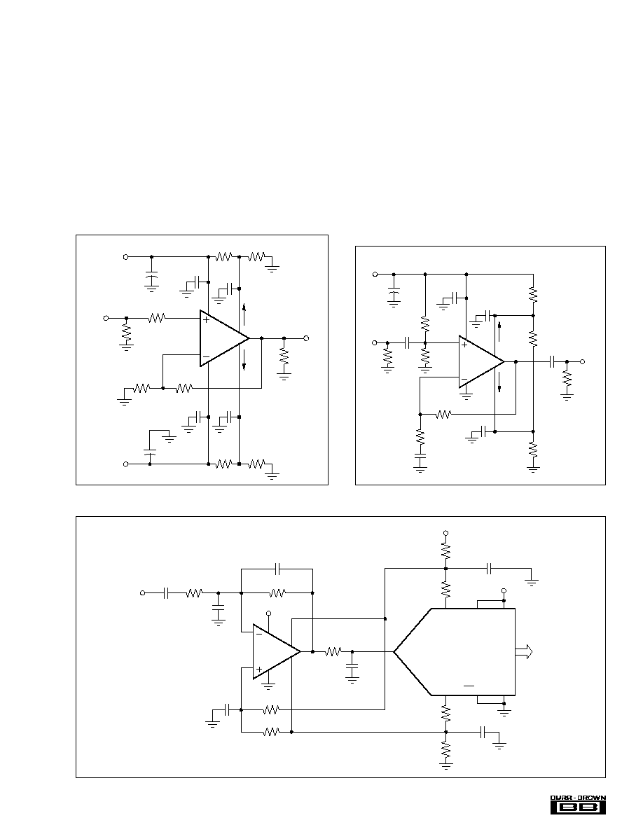
DUAL SUPPLY, NON-INVERTING AMPLIFIER
Figure 1 shows a non-inverting gain amplifier for dual
supply operation. This circuit was used for AC characteriza-
tion of the OPA689, with a 50
source, which it matches,
and a 500
load. The power supply bypass capacitors are
shown explicitly in Figures 1 and 2, but will be assumed in
the other figures. The limiter voltages (V
H
and V
L
) and their
bias currents (I
VH
and I
VL
) have the polarities shown.
SINGLE SUPPLY, NON-INVERTING AMPLIFIER
Figure 2 shows an AC coupled, non-inverting gain amplifier
for single supply operation. This circuit was used for AC
characterization of the OPA689, with a 50
source, which
it matches, and a 500
load. The power supply bypass
capacitors are shown explicitly in Figures 1 and 2, but will
be assumed in the other figures. The limiter voltages (V
H
and V
L
) and their bias currents (I
VH
and I
VL
) have the
polarities shown. Notice that the single supply circuit can
use 3 resistors to set V
H
and V
L
, where the dual supply
circuit usually uses 4 to reference the limit voltages to
ground.
LOW DISTORTION, ADC INPUT DRIVER
The circuit in Figure 3 shows an inverting, low distortion
ADC driver that operates on single supply. The converter's
internal references bias the op amp input. The 4.0pF and
18pF capacitors form a compensation network that allows
FIGURE 3. Low Distortion, Limiting ADC Input Driver.
FIGURE 1. DC-Coupled, Dual Supply Amplifier.
FIGURE 2. AC-Coupled, Single Supply Amplifier.
OPA689
49.9
6
I
VH
V
O
V
IN
I
VL
≠V
S
= ≠5V
3
2
4
7
8
5
R
F
750
R
G
150
500
0.1µF
0.1µF
0.1µF
100
3.01k
1.91k
3.01k
1.91k
0.1µF
V
H
= +2V
V
L
= ≠2V
+
2.2µF
+
2.2µF
+V
S
= +5V
OPA689
53.6
6
I
VH
V
H
= 3.7V
V
O
V
L
= 1.3V
V
IN
I
VL
1.50k
3
2
4
7
8
5
1.50k
523
976
523
R
G
150
R
F
750
500
0.1µF
0.1µF
0.1µF
+
2.2µF
0.1µF
V
S
= +5V
0.1µF
0.1µF
OPA689
V
S
= +5V
V
S
= +5V
4
3
2
7
5
8
6
V
S
= +5V
V
IN
4.0pF
750
0.1
µ
F
REFB
REFT
IN
INT/EXT
RSEL
+V
S
GND
0.1
µ
F
18pF
100pF
V
H
= +3.6V
V
L
= +1.4V
+2.5V
374
1.40k
24.9
1.40k
0.1
µ
F
0.1
µ
F
787
100
100
787
ADS822
10-Bit
40MSPS
10-Bit
Data
+1.5V
+3.5V
12
Æ
OPA689
the OPA689 to have a flat frequency response at a gain of ≠
2. This increases the loop gain of the op amp feedback
network, which reduces the distortion products below their
specified values.
PRECISION HALF WAVE RECTIFIER
Figure 4 shows a half wave rectifier with outstanding preci-
sion and speed. V
H
will default to a voltage between 3.1 and
3.8V if left open, while the negative limit is set to ground.
OPA689
6
V
O
≠V
S
= ≠5V
+V
S
= +5V
V
IN
2
3
4
7
8
5
750
150
124
NC
FIGURE 4. Precision Half Wave Rectifier.
VERY HIGH SPEED COMPARATOR
Figure 5 shows a very high speed comparator with hysterisis.
The output level are precisely defined, and the recovery time
is exceptional. The output voltage swings between 0.5V and
3.5V to provide a logic level output that switches as V
IN
crosses V
REF
.
OPA689
6
V
O
≠V
S
= ≠5V
3
2
4
7
8
5
0.1µF
0.1µF
2.00k
1.21k
200k
604
+V
S
= +5V
100
V
IN
95.3
FIGURE 5. Very High Speed Comparator.
FIGURE 6. Transimpedance Amplifier.
DESIGN-IN TOOLS
APPLICATIONS SUPPORT
The Burr-Brown Applications Department is available
for design assistance at phone number 1-800-548-6132
(US/Canada only). The Burr-Brown Internet web page
(http://www.burr-brown.com) has the latest data sheets and
other design aids.
DEMONSTRATION BOARDS
Two PC boards are available to assist in the initial evaluation
of circuit performance of the OPA689 in both package
styles. These will be available as an unpopulated PCB with
descriptive documentation. See the board literature for more
information. The summary information for these boards is
shown below:
BOARD
LITERATURE
PART
REQUEST
PRODUCT
PACKAGE
NUMBER
NUMBER
OPA689P
8-Pin DIP
DEM-OPA68xP
MKT-350
OPA689U
8-Pin SO-8
DEM-OPA68xU
MKT-351
Contact the Burr-Brown Applications Department for avail-
ability of these boards.
SPICE MODELS
Computer simulation of circuit performance using SPICE is
often useful when analyzing analog circuit or system perfor-
mance. This is particularly true for high speed amplifier
circuits where parasitic capacitance and inductance can have
a major effect on frequency response.
SPICE models are available through the Burr-Brown web
site (www.burr-brown.com). These models do a good job of
predicting small-signal AC and transient performance under
a wide variety of operating conditions. They do not do as
well in predicting the harmonic distortion, temperature ef-
fects, or different gain and phase characteristics. These
models do not distinquish between the AC performance of
different package types.
OPA689
+V
S
= +5V
NC
NC
≠V
S
= ≠5V
4
2
3
7
5
8
6
V
O
4.32k
4.32k
C
F
1.0pF
C
D
5.0pF
0.1
µ
F
≠V
B
I
D
TRANSIMPEDANCE AMPLIFIER
Figure 6 shows a transimpedance amplifier that has excep-
tional overdrive characteristics. The feedback capacitor (C
F
)
stabilizes the circuit for the assumed diode capacitance (C
D
).

13
Æ
OPA689
OPERATING INFORMATION
THEORY OF OPERATION
The OPA689 is a voltage feedback op amp that is stable for
gains
+4. The output voltage is limited to a range set by the
limiter pins (5 and 8). When the input tries to overdrive the
output, the limiters take control of the output buffer. This
avoids saturating any parts in the signal path, gives quick
overdrive recovery, and gives consistent limiter accuracy for
any gain.
This part is de-compensated (stable for gains
+4). This
gives greater bandwidth, higher slew rate, and lower noise
than the unity gain stable companion part OPA688.
The limiters have a very sharp transition from the linear
region of operation to output limiting. This allows the limiter
voltages to be set very near (<100 mV) the desired signal
range. The distortion performance is also very good near the
limiter voltages.
CIRCUIT LAYOUT
Achieving optimum performance with the high frequency
OPA689 requires careful attention to layout design and
component selection. Recommended PCB layout techniques
and component selection criteria are:
a) Minimize parasitic capacitance to any ac ground for all
of the signal I/O pins. Open a window in the ground and
power planes around the signal I/O pins, and leave the
ground and power planes unbroken elsewhere.
b) Provide a high quality power supply. Use linear regu-
lators, ground plane, and power planes, to provide power.
Place high frequency 0.1
µ
F decoupling capacitors < 0.2"
away from each power supply pin. Use wide, short traces to
connect to these capacitors to the ground and power planes.
Also use larger (2.2
µ
F to 6.8
µ
F) high frequency decoupling
capacitors to bypass lower frequencies. They may be some-
what further from the device, and be shared among several
adjacent devices.
c) Place external components close to the OPA689. This
minimizes inductance, ground loops, transmission line ef-
fects and propagation delay problems. Be extra careful with
the feedback (R
F
), input and output resistors.
d) Use high frequency components to minimize parasitic
elements. Resistors should be a very low reactance type.
Surface mount resistors work best and allow a tighter layout.
Metal film or carbon composition axially-leaded resistors
can also provide good performance when their leads are as
short as possible. Never use wire-wound resistors for high
frequency applications. Remember that most potentiometers
have large parasitic capacitances and inductances.
Multilayer ceramic chip capacitors work best and take up
little space. Monolithic ceramic capacitors also work very
well. Use RF type capacitors with low ESR and ESL. The
large power pin bypass capacitors (2.2
µ
F to 6.8
µ
F) should
be tantalum for better high frequency and pulse perfor-
mance.
e) Choose low resistor values to minimize the time constant
set by the resistor and its parasitic parallel capacitance. Good
metal film or surface mount resistors have approximately
0.2pF parasitic parallel capacitance. For resistors > 1.5k
,
this adds a pole and/or zero below 500MHz.
Make sure that the output loading is not too heavy. The
recommended 750
feedback resistor is a good starting
point in your design.
f) Use short direct traces to other wideband devices on
the board. Short traces act as a lumped capacitive load. Wide
traces (50 to 100 mils) should be used. Estimate the total
capacitive load at the output, and use the series isolation
resistor recommended in the R
S
vs Capacitive Load plot.
Parasitic loads < 2pF may not need the isolation resistor.
g) When long traces are necessary, use transmission line
design techniques (consult an ECL design handbook for
microstrip and stripline layout techniques). A 50
transmis-
sion line is not required on board--a higher characteristic
impedance will help reduce output loading. Use a matching
series resistor at the output of the op amp to drive a
transmission line, and a matched load resistor at the other
end to make the line appear as a resistor. If the 6dB of
attenuation that the matched load produces is not acceptable,
and the line is not too long, use the series resistor at the
source only. This will isolate the op amp output from the
reactive load presented by the line, but the frequency re-
sponse will be degraded.
Multiple destination devices are best handled as separate
transmission lines, each with its own series source and shunt
load terminations. Any parasitic impedances acting on the
terminating resistors will alter the transmission line match,
and can cause unwanted signal reflections and reactive
loading.
h) Do not use sockets for high speed parts like the OPA689.
The additional lead length and pin-to-pin capacitance intro-
duced by the socket creates an extremely troublesome para-
sitic network. Best results are obtained by soldering the part
onto the board. If socketing for DIP prototypes is desired,
high frequency flush mount pins (e.g., McKenzie Technol-
ogy #710C) can give good results.
POWER SUPPLIES
The OPA689 is nominally specified for operation using
either
±
5V supplies or a single +5V supply. The maximum
specified total supply voltage of 13V allows reasonable
tolerances on the supplies. Higher supply voltages can break
down internal junctions, possibly leading to catastrophic
failure. Single supply operation is possible as long as com-
mon mode voltage constraints are observed. The common
mode input and output voltage specifications can be inter-
preted as a required headroom to the supply voltage. Observ-
ing this input and output headroom requirement will allow
design of non-standard or single supply operation circuits.
Figure 2 shows one approach to single-supply operation.
14
Æ
OPA689
ESD PROTECTION
ESD damage is known to damage MOSFET devices, but any
semiconductor device is vulnerable to ESD damage. This is
particularly true for very high speed, fine geometry processes.
ESD damage can cause subtle changes in amplifier input
characteristics without necessarily destroying the device. In
precision operational amplifiers, this may cause a noticeable
degradation of offset voltage and drift. Therefore, ESD
handling precautions are required when handling the OPA689.
OUTPUT LIMITERS
The output voltage is linearly dependent on the input(s)
when it is between the limiter voltages V
H
(pin 8) and V
L
(pin 5). When the output tries to exceed V
H
or V
L
, the
corresponding limiter buffer takes control of the output
voltage and holds it at V
H
or V
L
.
Because the limiters act on the output, their accuracy does
not change with gain. The transition from the linear region
of operation to output limiting is sharp--the desired output
signal can safely come to within 30mV of V
H
or V
L
.
Distortion performance is also good over the same range.
The limiter voltages can be set to within 0.7V of the supplies
(V
L
≠V
S
+ 0.7V, V
H
+V
S
≠ 0.7V). They must also be at
least 200mV apart (V
H
≠ V
L
0.2V).
When pins 5 and 8 are left open, V
H
and V
L
go to the Default
Voltage Limit; the minimum values are in the spec table.
Looking at Figure 7 for the zero bias current case will show
the expected range of (V
S
≠ default limit voltages) = head-
room).
When the limiter voltages are more than 2.1V from the
supplies (V
L
≠V
S
+ 2.1V or V
H
+V
S
≠ 2.1V), you can
use simple resistor dividers to set V
H
and V
L
(see Figure 1).
Make sure you include the Limiter Input Bias Currents
(Figure 7) in the calculations (i.e., I
VL
≠50
µ
A out of pin
5, and I
VH
+50
µ
A out of pin 8). For good limiter voltage
accuracy, run at least 1mA quiescent bias current through
these resistors.
When the limiter voltages need to be within 2.1V of the
supplies (V
L
≠V
S
+ 2.1V or V
H
+V
S
≠ 2.1V), use low
impedance voltage sources to set V
H
and V
L
to minimize
errors due to bias current uncertainty. This will typically be
the case for single supply operation (V
S
= +5V). Figure 2
runs 2.5mA through the resistive divider that sets V
H
and
V
L
. This keeps errors due to I
VH
and I
VL
<
±
1% of the target
limit voltages.
The limiters' DC accuracy depends on attention to detail.
The two dominant error sources can be improved as follows:
∑ Power supplies, when used to drive resistive dividers that
set V
H
and V
L
, can contribute large errors (e.g., (5%).
Using a more accurate source, or bypassing pins 5 and 8
with good capacitors, will improve limiter PSRR.
∑ The resistor tolerances in the resistive divider can also
dominate. Use 1% resistors.
Other error sources also contribute, but should have little
impact on the limiters' DC accuracy:
∑ Reduce offsets caused by the Limiter Input Bias Currents.
Select the resistors in the resistive divider(s) as described
above.
∑ Consider the signal path DC errors as contributing to the
uncertainty in the useable output range.
∑ The Limiter Offset Voltage only slightly degrades the
limiter accuracy.
Figure 8 shows how the limiters affect distortion perfor-
mance. Virtually no degradation in linearity is observed for
output voltages swinging right up to the limiter voltages.
FIGURE 8. Linearity Guardband.
FIGURE 7. Limiter Bias Current vs Limiter Voltage.
HARMONIC DISTORTION NEAR LIMIT VOLTAGES
≠40
≠45
≠50
≠55
≠60
≠65
≠70
≠75
≠80
≠85
≠90
± Limit Voltage (V)
0.9
1.0
1.1
1.2
1.3
1.4
1.5
1.6
1.7
1.8
1.9
2.0
2nd and 3rd Harmonic Distortion (dBc)
V
O
= 0V
DC
±1Vp
f
1
= 5MHz
R
L
= 500
HD2
HD3
100
75
50
25
0
≠25
≠50
≠75
≠100
LIMITER INPUT BIAS CURRENT vs BIAS VOLTAGE
Limiter Headroom (V)
0.0
0.5
1.0
1.5
2.0
2.5
3.0
3.5
4.0
4.5
5.0
Limter Input Bias Current (
µ
A)
Maximum Over Temperature
Minimum Over Temperature
Limiter Headroom = +V
S
≠ V
H
Current = I
VH
or ≠I
VL
= V
L
≠ (≠V
S
)
15
Æ
OPA689
OPA689
C
L
R
L
R
ISO
R
L
is optional
V
O
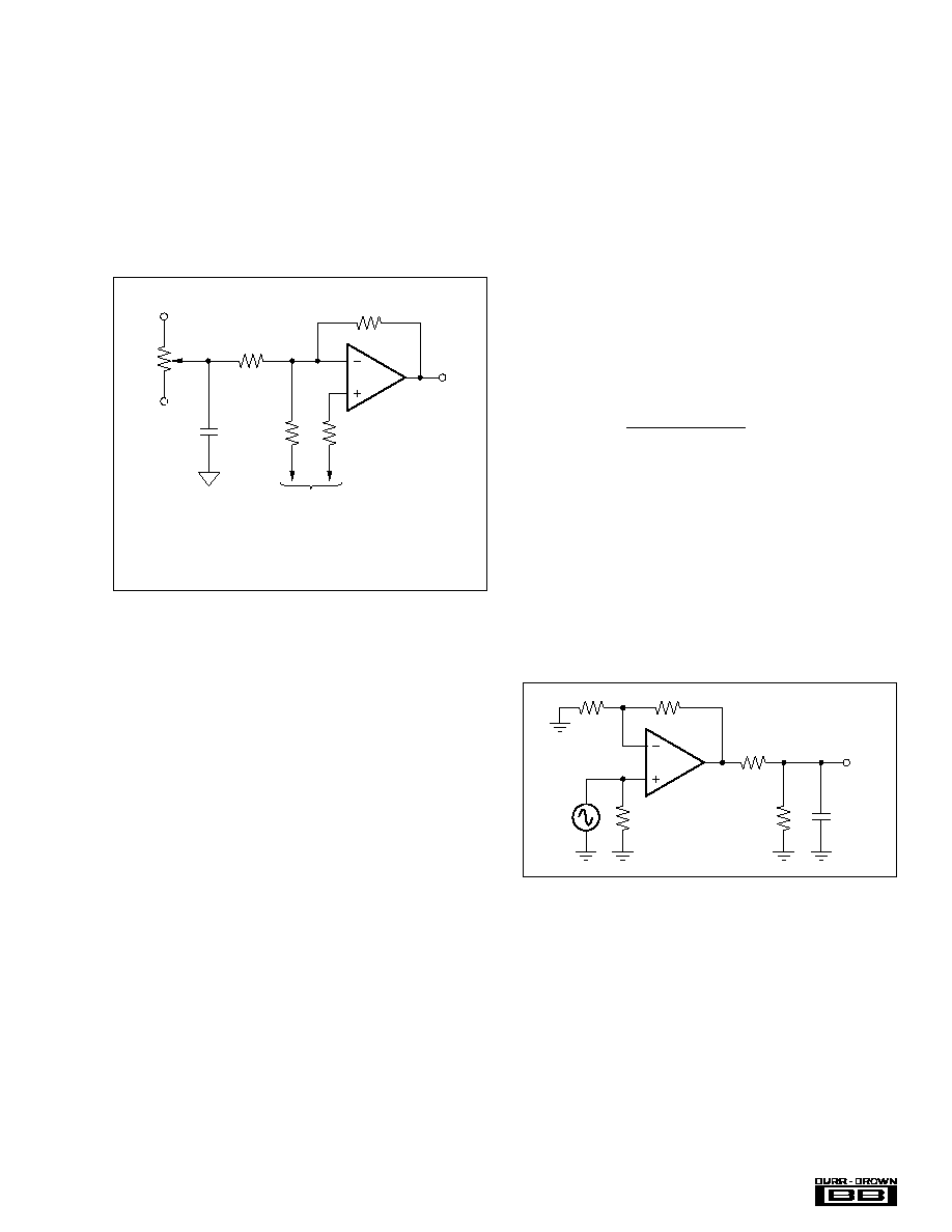
OFFSET VOLTAGE ADJUSTMENT
The circuit in Figure 9 allows offset adjustment without
degrading offset drift with temperature. Use this circuit with
caution since power supply noise can inadvertently couple
into the op amp.
Remember that additional offset errors can be created by the
amplifier's input bias currents. Whenever possible, match
the resistance seen by both DC Input Bias Currents by using
R
3
. This minimizes the output offset voltage caused by the
Input Bias Currents.
FIGURE 9. Offset Voltage Trim.
OUTPUT DRIVE
The OPA689 has been optimized to drive 500
loads, such
as A/D converters. It still performs very well driving 100
loads. This makes the OPA689 an ideal choice for a wide
range of high frequency applications.
Many high speed applications, such as driving A/D convert-
ers, require op amps with low output impedance. As shown
in the Output Impedance vs Frequency performance curve,
the OPA689 maintains very low closed-loop output imped-
ance over frequency. Closed-loop output impedance in-
creases with frequency since loop gain decreases with fre-
quency.
THERMAL CONSIDERATIONS
The OPA689 will not require heat-sinking under most oper-
ating conditions. Maximum desired junction temperature
will set a maximum allowed internal power dissipation as
described below. In no case should the maximum junction
temperature be allowed to exceed 175
∞
C.
The total internal power dissipation (P
D
) is the sum of
quiescent power (P
DQ
) and the additional power dissipated
in the output stage (P
DL
) while delivering load power. P
DQ
is simply the specified no-load supply current times the total
supply voltage across the part. P
DL
depends on the required
output signals and loads. For a grounded resistive load,
and equal bipolar supplies, it is at a maximum when the
output is at 1/2 either supply voltage. In this condition,
P
DL
= V
S
2
/(4R
L
) where R
L
includes the feedback network
loading. Note that it is the power in the output stage, and not
in the load, that determines internal power dissipation.
The operating junction temperature is: T
J
= T
A
+ P
D
JA
,
where T
A
is the ambient temperature.
For example, the maximum T
J
for a OPA689U with G = +6,
R
FB
= 750
, R
L
= 100
, and
±
V
S
=
±
5V at the maximum
T
A
= +85
∞
C is calculated this way:
P
DQ
= 10
V ∑
20
mA
(
)
= 200
mW
P
DL
=
5
V
( )
2
4
∑
100
||
850
(
)
P
D
= 200
mW
+ 70
mW
= 270
mW
T
J
= 85∞
C
+ 270
mW ∑
125∞
C/ W
= 119∞
C
CAPACITIVE LOADS
Capacitive loads, such as flash A/D converters, will decrease
the amplifier's phase margin, which may cause peaking or
oscillations. Capacitive loads
1pF should be isolated by
connecting a small resistor in series with the output as shown
in Figure 10. Increasing the gain from +6 will improve the
capacitive drive capabilities due to increased phase margin.
FIGURE 10. Driving Capacitive Loads.
In general, capacitive loads should be minimized for opti-
mum high frequency performance. The capacitance of coax
cable (29pF/foot for RG-58) will not load the amplifier
when the coaxial cable, or transmission line, is terminated in
its characteristic impedance.
R2
OPA689
R3 = R
1
|| R
2
R1
R
TRIM
47k
+V
S
V
O
≠V
S
V
IN
or Ground
0.1µF
NOTES: (1) R
3
is optional and minimizes
output offset due to input bias currents. (2) Set
R
1
<< R
TRIM
.
16
Æ
OPA689
FREQUENCY RESPONSE COMPENSATION
The OPA689 is internally compensated to be stable at a gain
of +4, and has a nominal phase margin of 60
∞
at a gain of +6.
Phase margin and peaking improve at higher gains. Recall
that an inverting gain of ≠5 is equivalent to a gain of +6 for
bandwidth purposes (i.e., noise gain = 6).
Standard external compensation techniques work with this
device. For example, in the inverting configuration, the
bandwidth may be limited without modifying the inverting
gain by placing a series RC network to ground on the
inverting node. This has the effect of increasing the noise
gain at high frequencies, which limits the bandwidth.
To maintain a large bandwidth at high gains, cascade several
op amps.
In applications where a large feedback resistor is required,
such as photodiode transimpedance amplifier, the parasitic
capacitance from the inverting input to ground causes peak-
ing or oscillations. To compensate for this effect, connect a
small capacitor in parallel with the feedback resistor. The
bandwidth will be limited by the pole that the feedback
resistor and this capacitor create. In other high gain applica-
tions, use a three resistor "Tee" network to reduce the RC
time constants set by the parasitic capacitances. Be careful
to not increase the noise generated by this feedback network
too much.
PULSE SETTLING TIME
The OPA689 is capable of an extremely fast settling time in
response to a pulse input. Frequency response flatness and
phase linearity are needed to obtain the best settling times.
For capacitive loads, such as an A/D converter, use the
recommended R
S
in the R
S
vs Capacitive Load plot. Ex-
tremely fine scale settling (0.01%) requires close attention to
ground return current in the supply decoupling capacitors.
The pulse settling characteristics when recovering from
overdrive are very good.
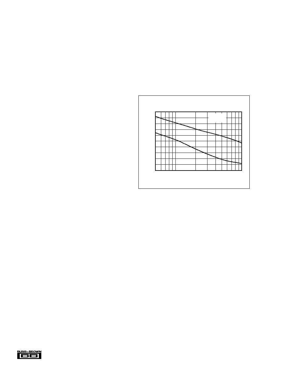
DISTORTION
The OPA689's distortion performance is specified for a
500
load, such as an A/D converter. Driving loads with
smaller resistance will increase the distortion as illustrated in
Figure 11. Remember to include the feedback network in the
load resistance calculations.
FIGURE 11. 5MHz Harmonic Distortion vs Load Resistance.
≠40
≠45
≠50
≠55
≠60
≠65
≠70
≠75
≠80
≠85
≠90
HARMONIC DISTORTION vs LOAD RESISTANCE
Load Resistance (
)
2nd and 3rd Harmonic Distortion (dBc)
50
100
1000
V
O
= 2Vp-p
f
1
= 5MHz
HD2
HD3

PACKAGING INFORMATION
ORDERABLE DEVICE
STATUS(1)
PACKAGE TYPE
PACKAGE DRAWING
PINS
PACKAGE QTY
OPA689P
ACTIVE
PDIP
P
8
50
OPA689U
ACTIVE
SOIC
D
8
100
OPA689U/2K5
ACTIVE
SOIC
D
8
2500
(1) The marketing status values are defined as follows:
ACTIVE: Product device recommended for new designs.
LIFEBUY: TI has announced that the device will be discontinued, and a lifetime-buy period is in effect.
NRND: Not recommended for new designs. Device is in production to support existing customers, but TI does not recommend using this part in
a new design.
PREVIEW: Device has been announced but is not in production. Samples may or may not be available.
OBSOLETE: TI has discontinued the production of the device.
PACKAGE OPTION ADDENDUM
www.ti.com
3-Oct-2003

IMPORTANT NOTICE
Texas Instruments Incorporated and its subsidiaries (TI) reserve the right to make corrections, modifications,
enhancements, improvements, and other changes to its products and services at any time and to discontinue
any product or service without notice. Customers should obtain the latest relevant information before placing
orders and should verify that such information is current and complete. All products are sold subject to TI's terms
and conditions of sale supplied at the time of order acknowledgment.
TI warrants performance of its hardware products to the specifications applicable at the time of sale in
accordance with TI's standard warranty. Testing and other quality control techniques are used to the extent TI
deems necessary to support this warranty. Except where mandated by government requirements, testing of all
parameters of each product is not necessarily performed.
TI assumes no liability for applications assistance or customer product design. Customers are responsible for
their products and applications using TI components. To minimize the risks associated with customer products
and applications, customers should provide adequate design and operating safeguards.
TI does not warrant or represent that any license, either express or implied, is granted under any TI patent right,
copyright, mask work right, or other TI intellectual property right relating to any combination, machine, or process
in which TI products or services are used. Information published by TI regarding third-party products or services
does not constitute a license from TI to use such products or services or a warranty or endorsement thereof.
Use of such information may require a license from a third party under the patents or other intellectual property
of the third party, or a license from TI under the patents or other intellectual property of TI.
Reproduction of information in TI data books or data sheets is permissible only if reproduction is without
alteration and is accompanied by all associated warranties, conditions, limitations, and notices. Reproduction
of this information with alteration is an unfair and deceptive business practice. TI is not responsible or liable for
such altered documentation.
Resale of TI products or services with statements different from or beyond the parameters stated by TI for that
product or service voids all express and any implied warranties for the associated TI product or service and
is an unfair and deceptive business practice. TI is not responsible or liable for any such statements.
Following are URLs where you can obtain information on other Texas Instruments products and application
solutions:
Products
Applications
Amplifiers
amplifier.ti.com
Audio
www.ti.com/audio
Data Converters
dataconverter.ti.com
Automotive
www.ti.com/automotive
DSP
dsp.ti.com
Broadband
www.ti.com/broadband
Interface
interface.ti.com
Digital Control
www.ti.com/digitalcontrol
Logic
logic.ti.com
Military
www.ti.com/military
Power Mgmt
power.ti.com
Optical Networking
www.ti.com/opticalnetwork
Microcontrollers
microcontroller.ti.com
Security
www.ti.com/security
Telephony
www.ti.com/telephony
Video & Imaging
www.ti.com/video
Wireless
www.ti.com/wireless
Mailing Address:
Texas Instruments
Post Office Box 655303 Dallas, Texas 75265
Copyright
2003, Texas Instruments Incorporated