Document Outline
- FEATURES
- APPLICATIONS
- DESCRIPTION
- OPA695 RELATED PRODUCTS
- ABSOLUTE MAXIMUM RATINGS(
- PACKAGE/ORDERING INFORMATION
- PIN CONFIGURATIONS
- ELECTRICAL CHARACTERISTICS: VS = ±5V
- ELECTRICAL CHARACTERISTICS: VS = + 5V
- TYPICAL CHARACTERISTICS: VS = ±5V
- TYPICAL CHARACTERISTICS: VS = ±5V Differential Operation
- APPLICATIONS INFORMATION
- WIDEBAND CURRENT FEEDBACK OPERATION
- RF SPECIFICATIONS AND APPLICATIONS
- INPUT RETURN LOSS ( S11)
- OUTPUT RETURN LOSS ( S22)
- FORWARD GAIN ( S21)
- REVERSE ISOLATION ( S12)
- LIMITS TO DYNAMIC RANGE
- -1dB COMPRESSION
- TWO-TONE 3rd-ORDER OUTPUT INTERMODULATION INTERCEPT ( OP3 )
- NOISE FIGURE
- SAW FILTER BUFFER
- LO BUFFER AMPLIFIER
- WIDEBAND CABLE DRIVING APPLICATIONS
- CABLE MODEM RETURN PATH DRIVER
- RGB VIDEO LINE DRIVER
- ARBITRARY WAVEFORM DRIVER
- DIFFERENTIAL I/O APPLICATIONS
- DESIGN-IN TOOLS
- OPERATING SUGGESTIONS
- SETTING RESISTOR VALUES TO OPTIMIZE BANDWIDTH
- OUTPUT CURRENT AND VOLTAGE
- DRIVING CAPACITIVE LOADS
- DISTORTION PERFORMANCE
- NOISE PERFORMANCE
- DC ACCURACY AND OFFSET CONTROL
- POWER SHUTDOWN OPERATION
- THERMAL ANALYSIS
- BOARD LAYOUT GUIDELINES
- INPUT AND ESD PROTECTION
- PACKAGE DRAWINGS
- D (R-PDSO-G**) PLASTIC SMALL-OUTLINE PACKAGE
- DBV (R-PDO-G6) PLASTIC SMALL-OUTLINE PACKAGE
- IMPORTANT NOTICE
PRODUCTION DATA information is current as of publication date.
Products conform to specifications per the terms of Texas Instruments
standard warranty. Production processing does not necessarily include
testing of all parameters.
DESCRIPTION
The OPA695 is a very high bandwidth, current-feedback op
amp that combines exceptional 4300V/
µ
s slew rate and low
input voltage noise to deliver a precision low cost, high
dynamic range Intermediate Frequency (IF) amplifier. Opti-
mized for high gain operation, the OPA695 is ideally suited to
buffering Surface Acoustic Wave (SAW) filters in an IF strip
or delivering high output power at low distortion for cable
modem upstream line drivers. Even higher bandwidth at
lower gains gives a 1400MHz video line driver for high
resolution RGB.
FEATURES
q
GAIN = +2 BANDWIDTH (1400MHz)
q
GAIN = +8 BANDWIDTH (450MHz)
q
OUTPUT VOLTAGE SWING:
±
4.2V
q
ULTRA-HIGH SLEW RATE: 4300V/
µ
s
q
3RD-ORDER INTERCEPT: > 40dBm (f < 50MHz)
q
LOW POWER: 129mW
q
LOW DISABLED POWER: 0.5mW
APPLICATIONS
q
VERY WIDEBAND ADC DRIVER
q
LOW-COST PRECISION IF AMPLIFIER
q
BROADBAND VIDEO LINE DRIVER
q
PORTABLE INSTRUMENTS
q
ACTIVE FILTERS
q
ARB WAVEFORM OUTPUT DRIVER
q
OPA685 PERFORMANCE UPGRADE
OPA695 RELATED PRODUCTS
SINGLES
DUALS
OPA658
OPA2658
OPA691
OPA2691
OPA692
THS3202
OPA693
--
The OPA695's low 12.9mA supply current is precisely
trimmed at +25
∞
C. This trim, along with a low temperature
drift, gives low system power over temperature. System
power may be further reduced using the optional disable
control pin. Leaving this pin open, or holding it HIGH, gives
normal operation. If pulled LOW, the OPA695 supply current
drops to less than 170
µ
A. This power-saving feature, along
with exceptional single +5V operation and ultra-small
SOT23-6 packaging, make the OPA695 ideal for portable
applications.
OPA6
95
OPA6
95
OPA695
SBOS293B ≠ DECEMBER 2003 ≠ REVISED MARCH 2004
www.ti.com
Copyright © 2003-2004, Texas Instruments Incorporated
Ultra-Wideband, Current-Feedback
OPERATIONAL AMPLIFIER With Disable
Please be aware that an important notice concerning availability, standard warranty, and use in critical applications of
Texas Instruments semiconductor products and disclaimers thereto appears at the end of this data sheet.
All trademarks are the property of their respective owners.
OPA695
+5V
511
75
75
V
LOAD
V
IN
RG-59
75
511
-
5V
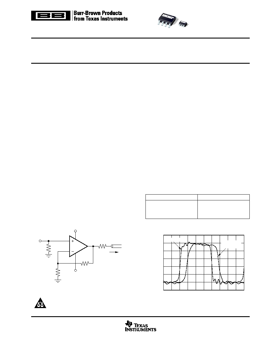
Gain 2V/V Video Line Driver
1.2
1
0.8
0.6
0.4
0.2
0
-
0.2
Time (1ns/div)
GAIN OF +2V/V VIDEO LINE DRIVER
PULSE RESPONSE
Input/Load Voltage (V)
Voltage at
Matched Load
125MHz Input
OPA695
2
SBOS293B
www.ti.com
SPECIFIED
PACKAGE
TEMPERATURE
PACKAGE
ORDERING
TRANSPORT
PRODUCT
PACKAGE-LEAD
DESIGNATOR
(1)
RANGE
MARKING
NUMBER
MEDIA, QUANTITY
OPA695
SO-8
D
≠40
∞
C to +85
∞
C
OPA695
OPA695ID
Rails, 100
"
"
"
"
"
OPA695IDR
Tape and Reel, 2500
OPA695
SOT23-6
(2)
DBV
≠40
∞
C to +85
∞
C
A71L
OPA695IDBVT
Tape and Reel, 250
"
"
"
"
"
OPA695IDBVR
Tape and Reel, 3000
ABSOLUTE MAXIMUM RATINGS
(1)
Power Supply ...............................................................................
±
6.5V
DC
Internal Power Dissipation ..................................... See Thermal Analysis
Differential Input Voltage ..................................................................
±
1.2V
Input Common-Mode Voltage Range .................................................
±
V
S
Storage Temperature Range: D, DBV ........................... ≠40
∞
C to +125
∞
C
Lead Temperature (soldering, 10s) .............................................. +300
∞
C
Junction Temperature (T
J
) ........................................................... +150
∞
C
ESD Rating
Human Body Model (HBM)
(2)
.......................................................... 1500V
Charge Device Model (CDM) .......................................................... 1000V
Machine Model (MM) ......................................................................... 100V
NOTES: (1) Stresses above these ratings may cause permanent damage.
Exposure to absolute maximum conditions for extended periods
may degrade device reliability. These are stress ratings only, and
functional operation of the device at these or any other conditions
beyond those specified is not supported.
(2) Pin 2 on SO-8 package and pin 4 on SOT23-6 package > 500V
HBM.
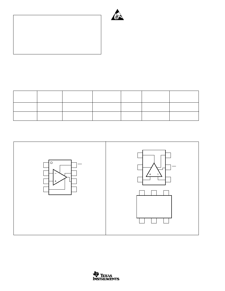
PIN CONFIGURATIONS
Top View
SO
NC = No Connection
Top View
SOT23-6
1
2
3
4
8
7
6
5
NC
Inverting Input
Noninverting Input
≠V
S
DIS
+V
S
Output
NC
1
2
3
6
5
4
Output
≠V
S
Noninverting Input
+V
S
DIS
Inverting Input
1
2
3
6
5
4
Pin Orientation/Package Marking
A71L
ELECTROSTATIC
DISCHARGE SENSITIVITY
This integrated circuit can be damaged by ESD. Texas Instru-
ments recommends that all integrated circuits be handled with
appropriate precautions. Failure to observe proper handling
and installation procedures can cause damage.
ESD damage can range from subtle performance degradation
to complete device failure. Precision integrated circuits may be
more susceptible to damage because very small parametric
changes could cause the device not to meet its published
specifications.
PACKAGE/ORDERING INFORMATION
NOTE: (1) For the most current specifications and package information, refer to our web site at www.ti.com.
(2) The SOT23-6 is shipped only as a lead-free and
green package. Check TI web site for lead-free availability of other packages.

OPA695
3
SBOS293B
www.ti.com
ELECTRICAL CHARACTERISTICS: V
S
=
±
5V
Boldface limits are tested at +25
∞
C.
R
F
= 402
, R
L
= 100
, and G = +8
,
(see Figure 1 for AC performance only), unless otherwise noted.
OPA695ID, IDBV
TYP
MIN/MAX OVER TEMPERATURE
0
∞
C to
≠40
∞
C to
MIN/
TEST
PARAMETER
CONDITIONS
+25
∞
C
+25
∞
C
(1)
70
∞
C
(2)
+85
∞
C
(2)
UNITS
MAX
LEVEL
(3)
AC PERFORMANCE (see Figure 1)
Small-Signal Bandwidth (V
O
= 0.5V
PP
)
G = +1, R
F
= 523
1700
MHz
typ
C
G = +2, R
F
= 511
1400
MHz
typ
C
G = +8, R
F
= 402
450
400
380
350
MHz
min
B
G = +16, R
F
= 249
350
MHz
typ
C
Bandwidth for 0.2dB Gain Flatness
G = +2, V
O
= 0.5V
PP
, R
F
=523
320
MHz
min
B
Peaking at a Gain of +1
R
F
= 523
, V
O
= 0.5V
PP
4.6
5.4
5.8
6.0
dB
max
B
Large-Signal Bandwidth
G = +8, V
O
= 4V
PP
450
MHz
typ
C
Slew Rate
G = ≠8, V
O
= 4V Step
4300
3700
3600
3500
V/
µ
s
min
B
G = +8, V
O
= 4V Step
2900
2600
2500
2400
V/
µ
s
min
B
Rise-and-Fall Time
G = +8, V
O
= 0.5V Step
0.8
ns
typ
C
G = +8, V
O
= 4V Step
1.0
ns
typ
C
Settling Time to 0.02%
G = +8, V
O
= 2V Step
16
ns
typ
C
0.1%
G = +8, V
O
= 2V Step
10
ns
typ
C
Harmonic Distortion
G = +8, f = 10MHz, V
O
= 2V
PP
2nd-Harmonic
R
L
= 100
≠65
≠62
≠60
≠59
dBc
max
B
R
L
500
≠78
≠76
≠74
≠73
dBc
max
B
3rd-Harmonic
R
L
= 100
≠86
≠84
≠75
≠72
dBc
max
B
R
L
500
≠86
≠82
≠81
≠80
dBc
max
B
Input Voltage Noise
f > 1MHz
1.8
2
2.7
2.9
nV/
Hz
max
B
Noninverting Input Current Noise
f > 1MHz
18
19
21
22
pA/
Hz
max
B
Inverting Input Current Noise
f > 1MHz
22
24
26
27
pA/
Hz
max
B
Differential Gain
G = +2, NTSC, V
O
= 1.4Vp, R
L
= 150
0.04
%
typ
C
Differential Phase
G = +2, NTSC, V
O
= 1.4Vp, R
L
= 150
0.007
deg
typ
C
DC PERFORMANCE
(4)
Open-Loop Transimpedance Gain (Z
OL
)
V
O
= 0V, R
L
= 100
85
45
43
41
k
min
A
Input Offset Voltage
V
CM
= 0V
±
0.3
±
3.0
±
3.5
±
4.0
mV
max
A
Average Offset Voltage Drift
V
CM
= 0V
±
10
±
15
µ
V/
∞
C
max
B
Noninverting Input Bias Current
V
CM
= 0V
+13
±
30
±
37
±
41
µ
A
max
A
Average Noninverting Input Bias Current Drift
V
CM
= 0V
+150
+180
nA/
∞
C
max
B
Inverting Input Bias Current
V
CM
= 0V
±
20
±
60
±
66
±
70
µ
A
max
A
Average Inverting Input Bias Current Drift
V
CM
= 0V
±
120
±
160
nA
∞
/C
max
B
INPUT
Common-Mode Input Range
(5)
(CMIR)
±
3.3
±
3.1
±
3.0
±
3.0
V
min
A
Common-Mode Rejection Ratio (CMRR)
V
CM
= 0V
56
51
50
50
dB
min
A
Noninverting Input Impedance
280 || 1.2
k
|| pF
typ
C
Inverting Input Resistance (R
I
)
Open-Loop
29
typ
C
OUTPUT
Voltage Output Swing
No Load
±
4.2
±
4.0
±
3.9
±
3.9
V
min
A
100
Load
±
3.9
±
3.7
±
3.7
±
3.6
V
min
A
Current Output, Sourcing
V
O
= 0
+120
+90
+80
+70
mA
min
A
Current Output, Sinking
V
O
= 0
≠120
≠90
≠80
≠70
mA
min
A
Closed-Loop Output Impedance
G = +8, f = 100kHz
0.04
typ
C
DISABLE (Disabled LOW)
Power-Down Supply Current (+V
S
)
V
DIS
= 0
≠100
≠170
≠186
≠192
µ
A
typ
A
Disable Time
V
IN
=
±
0.25V
DC
1
µ
s
typ
C
Enable Time
V
IN
=
±
0.25V
DC
25
ns
typ
C
Off Isolation
G = +8, 10MHz
70
dB
typ
C
Output Capacitance in Disable
4
pF
typ
C
Turn On Glitch
G = +2, R
L
= 150
, V
IN
= 0
±
100
mV
typ
C
Turn Off Glitch
G = +2, R
L
= 150
, V
IN
= 0
±
20
mV
typ
C
Enable Voltage
3.3
3.5
3.6
3.7
V
min
A
Disable Voltage
1.8
1.7
1.6
1.5
V
max
A
Control Pin Input Bias Current (DIS)
V
DIS
= 0
75
130
143
145
µ
A
max
A
POWER SUPPLY
Specified Operating Voltage
±
5
V
typ
C
Maximum Operating Voltage Range
±
6
±
6
±
6
V
max
A
Max Quiescent Current
V
S
=
±
5V
12.9
13.3
13.7
14.1
mA
max
A
Min Quiescent Current
V
S
=
±
5V
12.9
12.6
11.8
11.0
mA
min
A
Power-Supply Rejection Ratio (≠PSRR)
Input Referred
55
51
48
48
dB
typ
A
TEMPERATURE RANGE
Specification: ID, IDBV
≠40 to +85
∞
C
typ
C
Thermal Resistance,
JA
Junction-to-Ambient
D
SO-8
125
∞
C/W
typ
C
DBV
SOT23-6
150
∞
C/W
typ
C
NOTES: (1) Junction temperature = ambient for +25
∞
C specifications.
(2) Junction temperature = ambient at low temperature limit; junction temperature = ambient +15
∞
C at high temperature limit for over temperature
specifications.
(3) Test levels: (A) 100% tested at +25
∞
C. Over temperature limits by characterization and simulation.
(B) Limits set by characterization and simulation. (C) Typical value only for information.
(4) Current is considered positive out-of-node. V
CM
is the input common-mode voltage.
(5) Tested < 3dB below minimum specified CMRR at
±
CMIR limits.

OPA695
4
SBOS293B
www.ti.com
OPA695ID, IDBV
TYP
MIN/MAX OVER TEMPERATURE
0
∞
C to
≠40
∞
C to
MIN/
TEST
PARAMETER
CONDITIONS
+25
∞
C
+25
∞
C
(1)
70
∞
C
(2)
+85
∞
C
(2)
UNITS
MAX
LEVEL
(3)
ELECTRICAL CHARACTERISTICS: V
S
= +5V
Boldface limits are tested at +25
∞
C.
R
F
= 348
, R
L
= 100
to V
S
/2, and G = +8
,
(see Figure 3 for AC performance only), unless otherwise noted.
AC PERFORMANCE (see Figure 3)
Small-Signal Bandwidth (V
O
= 0.5V
PP
)
G = +1, R
F
= 511
1400
MHz
typ
C
G = +2, R
F
= 487
960
MHz
min
C
G = +8, R
F
= 348
395
380
330
300
MHz
typ
B
G = +16, R
F
= 162
235
MHz
typ
C
Bandwidth for 0.2dB Gain Flatness
G = +2, V
O
< 0.5V
PP
, R
F
= 487
230
180
135
110
MHz
min
B
Peaking at a Gain of +1
R
F
= 511
, V
O
< 0.5V
PP
1.0
2.0
2.5
3.0
dB
max
B
Large-Signal Bandwidth
G = +8, V
O
= 2V
PP
310
MHz
typ
C
Slew Rate
G = +8, 2V Step
1700
1300
1200
1100
V/
µ
s
min
B
Rise-and-Fall Time
G = +8, V
O
= 0.5V Step
1.0
ns
typ
C
G = +8, V
O
= 2V Step
1.0
ns
typ
C
Settling Time to 0.02%
G = +8, V
O
= 2V Step
16
ns
typ
C
0.1%
G = +8, V
O
= 2V Step
10
ns
typ
C
Harmonic Distortion
G = +8, f = 10MHz, V
O
= 2V
PP
2nd-Harmonic
R
L
= 100
to V
S
/2
≠62
≠58
≠58
≠57
dBc
max
B
R
L
500
to V
S
/2
≠70
≠66
≠66
≠65
dBc
max
B
3rd-Harmonic
R
L
= 100
to V
S
/2
≠66
≠64
≠64
≠63
dBc
max
B
R
L
500
to V
S
/2
≠65
≠63
≠63
≠62
dBc
max
B
Input Voltage Noise
f > 1MHz
1.8
2
2.7
2.9
nV/
Hz
max
B
Noninverting Input Current Noise
f > 1MHz
18
19
21
22
pA/
Hz
max
B
Inverting Input Current Noise
f > 1MHz
22
24
26
27
pA/
Hz
max
B
DC PERFORMANCE
(4)
Open-Loop Transimpedance Gain (Z
OL
)
V
O
= V
S
/2, R
L
= 100
to V
S
/2
70
40
38
36
k
min
A
Input Offset Voltage
V
CM
= V
S
/2
±
0.3
±
3
±
3.5
±
4.0
mV
max
A
Average Offset Voltage Drift
V
CM
= V
S
/2
±
10
±
15
µ
V/
∞
C
max
B
Noninverting Input Bias Current
V
CM
= V
S
/2
±
5
±
40
±
45
±
50
µ
A
max
A
Average Noninverting Input Bias Current Drift
V
CM
= V
S
/2
±
110
±
170
nA/
∞
C
max
B
Inverting Input Bias Current
V
CM
= V
S
/2
±
5
±
60
±
66
±
70
µ
A
max
A
Average Inverting Input Bias Current Drift
V
CM
= V
S
/2
±
120
±
160
nA /
∞
C
max
B
INPUT
Least Positive Input Voltage
(5)
1.7
1.8
1.9
1.9
V
max
A
Most Positive Input Voltage
(5)
3.3
3.2
3.1
3.1
V
min
A
Common-Mode Rejection Ratio (CMRR)
V
CM
= V
S
/2
54
51
50
50
dB
min
A
Noninverting Input Impedance
280 || 1.2
k
|| pF
typ
C
Inverting Input Resistance (R
I
)
Open-Loop
32
typ
C
OUTPUT
Most Positive Output Voltage
No Load
4.2
4.0
3.9
3.8
V
min
A
R
L
= 100
to V
S
/2
4.0
3.9
3.8
3.7
V
min
A
Least Positive Output Voltage
No Load
0.8
1.0
1.1
1.2
V
max
A
R
L
= 100
to V
S
/2
1.0
1.1
1.2
1.3
V
max
A
Current Output, Sourcing
V
O
= V
S
/2
90
70
67
66
mA
min
A
Current Output, Sinking
V
O
= V
S
/2
≠90
≠70
≠67
≠66
mA
min
A
Closed-Loop Output Impedance
G = +2, f = 100kHz
0.05
typ
C
DISABLE (Disabled LOW)
Power Down Supply Current (+V
S
)
V
DIS
= 0
≠95
≠160
≠175
≠180
µ
A
typ
C
Disable Time
1
µ
s
typ
C
Enable Time
25
ns
typ
C
Off Isolation
G = +8, 10MHz
70
dB
typ
C
Output Capacitance in Disable
4
pF
typ
C
Turn On Glitch
G = +2, R
L
= 150
, V
IN
= V
S
/2
±
100
mV
typ
C
Turn Off Glitch
G = +2, R
L
= 150
, V
IN
= V
S
/2
±
20
mV
typ
C
Enable Voltage
3.3
3.5
3.6
3.7
V
min
A
Disable Voltage
1.8
1.7
1.6
1.5
V
max
A
Control Pin Input Bias Current (DIS)
V
DIS
= 0
75
130
143
149
µ
A
typ
C
POWER SUPPLY
Specified Single-Supply Operating Voltage
5
V
typ
C
Max Single-Supply Operating Voltage
12
12
12
V
max
A
Max Quiescent Current
V
S
= +5V
11.4
12.0
12.5
12.9
mA
max
A
Min Quiescent Current
V
S
= +5V
11.4
10.9
9.4
9.1
mA
min
A
Power-Supply Rejection Ratio (≠PSRR)
Input Referred
56
dB
typ
C
TEMPERATURE RANGE
Specification: ID, IDBV
≠40 to +85
∞
C
typ
C
Thermal Resistance,
JA
Junction-to-Ambient
D
SO-8
125
∞
C/W
typ
C
DBV
SOT23-6
150
∞
C/W
typ
C
NOTES: (1) Junction temperature = ambient for +25
∞
C specifications.
(2) Junction temperature = ambient at low temperature limit: junction temperature = ambient +15
∞
C at high temperature limit for over temperature
specifications.
(3) Test levels: (A) 100% tested at +25
∞
C. Over temperature limits by characterization and simulation.
(B) Limits set by characterization and simulation. (C) Typical value only for information.
(4) Current is considered positive out-of-node. V
CM
is the input common-mode voltage.
(5) Tested < 3dB below minimum specified CMRR at
±
CMIR limits.
OPA695
5
SBOS293B
www.ti.com
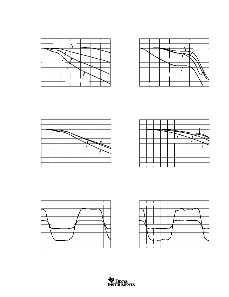
TYPICAL CHARACTERISTICS: V
S
=
±
5V
G = +8, R
F
= 402
, R
L
= 100
,
unless otherwise noted.
6
3
0
≠3
≠6
≠9
≠12
≠15
≠18
≠21
≠24
Frequency (MHz)
0
200
400
1400
1200
1000
600
800
NONINVERTING SMALL-SIGNAL
FREQUENCY RESPONSE
Normalized Gain (3dB/div)
G = +16, R
F
= 249
G = +8, R
F
= 402
See Figure 1
G = +2, R
F
= 523
V
O
= 500mV
PP
G = +4, R
F
= 480
6
3
0
≠3
≠6
≠9
≠12
≠15
≠18
≠21
≠24
Frequency (MHz)
0
200
400
1400
1200
1000
600
800
INVERTING SMALL-SIGNAL
FREQUENCY RESPONSE
Normalized Gain (3dB/div)
G = ≠8, R
F
= 442
G = ≠4,
R
F
= 475
See Figure 2
G = ≠2, R
F
= 499
V
O
= 500mV
PP
G = ≠16, R
F
= 806
24
21
18
15
12
9
6
3
0
≠3
≠6
Frequency (100MHz/div)
0
1GHz
500MHz
NONINVERTING LARGE-SIGNAL
FREQUENCY RESPONSE
Gain (3dB/div)
V
O
= 7V
PP
V
O
= 4V
PP
G = +8, R
F
= 402
See Figure 1
V
O
= 1V
PP
and 2V
PP
24
21
18
15
12
9
6
3
0
≠3
≠6
Frequency (100MHz/div)
0
1GHz
500MHz
INVERTING LARGE-SIGNAL
FREQUENCY RESPONSE
Gain (3dB/div)
V
O
= 7V
PP
V
O
= 2V
PP
V
O
= 1V
PP
V
O
= 4V
PP
G = ≠8, R
F
= 442
See Figure 2
3
2
1
0
≠1
≠2
≠3
Time (1ns/div)
NONINVERTING LARGE AND SMALL-SIGNAL
PULSE RESPONSE
Output Voltage
See Figure 1
G = +8, R
F
= 402
125MHz Square Wave Input
Small-Signal
±
500mV
Large-Signal
±
2V
3
2
1
0
≠1
≠2
≠3
Time (1ns/div)
INVERTING LARGE AND SMALL-SIGNAL
PULSE RESPONSE
Output Voltage
See Figure 2
G = +8, R
F
= 402
125MHz Square Wave Input
Small-Signal
±
500mV
Large-Signal
±
2V
OPA695
6
SBOS293B
www.ti.com
TYPICAL CHARACTERISTICS: V
S
=
±
5V
G = +8, R
F
= 402
, R
L
= 100
,
unless otherwise noted.
≠50
≠60
≠70
≠80
≠90
≠100
10MHz HARMONIC DISTORTION
vs LOAD RESISTANCE
Load Resistance (
)
50
100
500
Harmonic Distortion (dBc)
2nd-Harmonic
3rd-Harmonic
V
O
= 2V
PP
G = 8V/V
See Figure 1
≠55
≠60
≠65
≠70
≠75
≠80
≠85
≠90
≠95
10MHz HARMONIC DISTORTION
vs SUPPLY VOLTAGE
Supply Voltage (
±
V)
2.5
3.0
3.5
4.0
4.5
5.0
5.5
6.0
Harmonic Distortion (dBc)
See Figure 1
V
O
= 2V
PP
, G = 8V/V
R
L
= 100
2nd-Harmonic
3rd-Harmonic
≠50
≠60
≠70
≠80
≠90
≠100
HARMONIC DISTORTION vs FREQUENCY
Frequency (MHz)
0.5
1
10
100
Harmonic Distortion (dBc)
See Figure 1
V
O
= 2V
PP
, G = +8V/V
R
L
= 100
2nd-Harmonic
3rd-Harmonic
≠50
≠60
≠70
≠80
≠90
≠100
10MHz HARMONIC DISTORTION
vs OUTPUT VOLTAGE
Output Voltage (V
PP
)
0.1
1
5
Harmonic Distortion (dBc)
See Figure 1
G = +8V/V
R
L
= 100
2nd-Harmonic
3rd-Harmonic
≠60
≠65
≠70
≠75
≠80
≠85
≠90
10MHz HARMONIC DISTORTION
vs NONINVERTING GAIN
Noninverting Gain (V/V)
2
10
20
Harmonic Distortion (dBc)
See Figure 1
V
O
= 2V
PP
R
L
= 100
2nd-Harmonic
3rd-Harmonic
≠55
≠60
≠65
≠70
≠75
≠80
≠85
≠90
10MHz HARMONIC DISTORTION
vs INVERTING GAIN
Inverting Gain (|V/V|)
2
10
20
Harmonic Distortion (dBc)
See Figure 2
V
O
= 2V
PP
, R
L
= 100
2nd-Harmonic
3rd-Harmonic
OPA695
7
SBOS293B
www.ti.com
TYPICAL CHARACTERISTICS: V
S
=
±
5V
G = +8, R
F
= 402
, R
L
= 100
,
unless otherwise noted.
100
10
1
INPUT VOLTAGE AND CURRENT NOISE DENSITY
Frequency (Hz)
10
3
10
4
10
5
10
6
10
7
10
8
Current Noise (pA/
Hz)
Voltage Noise (nV/
Hz)
Noninverting Input Current Noise
Inverting Input Current Noise
19pA/
Hz
22pA/
Hz
Input Voltage Noise
1.7nV/
Hz
45
40
35
30
25
20
15
Frequency (MHz)
20
40
60
80
140 160
240
180 200 220
100 120
TWO-TONE, 3rd-ORDER
INTERMODULATION INTERCEPT
±
5V
Output Intercept (+dBm)
OPA685
P
I
P
O
402
50
50
50
56.2
G = 12dB to matched load.
OPA685
P
I
P
O
402
50
50
50
G = 12dB to matched load.
G = +8
G = ≠8
Noninverting
Inverting
0
≠10
≠20
≠30
≠40
≠50
≠60
INPUT RETURN LOSS vs FREQUENCY (S
11
)
Frequency (Hz)
10M
100M
1G
Return Loss (5dB/div)
G = +8
(see Figure 1)
G = ≠8
(see Figure 2)
VSWR < 1.2:1
0
≠10
≠20
≠30
≠40
≠50
≠60
OUTPUT RETURN LOSS vs FREQUENCY (S
22
)
Frequency (Hz)
10M
100M
1G
Return Loss (5dB/div)
G =
±
8V/V
Without
Trim Cap
With
Trim Cap
VSWR < 1.2:1
OPA695
50
2.5pF
S
22
Trim Cap
35
30
25
20
15
10
5
0
R
S
vs CAPACITIVE LOAD
Capacitive Load (pF)
5
10
100
R
S
(
)
0.5dB Peaking
Allowed
21
18
15
12
9
SMALL-SIGNAL FREQUENCY RESPONSE
vs CAPACITIVE LOAD
Frequency (Hz)
10M
100M
1G
Normalized Gain (dB)
OPA695
402
57.4
50
1k
V
I
+5V
≠5V
1k
load is optional
V
O
R
S
C
L
C
L
= 100pF
C
L
= 10pF
C
L
= 20pF
C
L
= 50pF
OPA695
8
SBOS293B
www.ti.com
TYPICAL CHARACTERISTICS: V
S
=
±
5V
G = +8, R
F
= 402
, R
L
= 100
,
unless otherwise noted.
60
55
50
45
40
35
30
25
20
10
3
10
4
10
5
10
6
10
7
10
8
CMRR AND PSRR vs FREQUENCY
Frequency (Hz)
Rejection Ratio (dB)
≠PSRR
+PSRR
CMRR
100
90
80
70
60
50
40
30
20
10
0
0
≠20
≠40
≠60
≠80
≠100
≠120
≠140
≠160
≠180
≠200
10
5
10
6
10
7
10
8
10
9
OPEN-LOOP TRANSIMPEDANCE GAIN AND PHASE
Frequency (Hz)
Open-Loop T
ransimpedance
Gain (dB
)
Open-Loop Phase (
∞
)
20 log| Z
OL
|
Z
OL
OUTPUT VOLTAGE AND CURRENT LIMITATIONS
5
4
3
2
1
0
≠1
≠2
≠3
≠4
≠5
I
O
(mA)
≠250 ≠200
≠100 ≠50
≠150
0
50
100
150
200
250
V
O
(V)
100
Load Line
1 Watt
Internal Power
1 Watt
Internal Power
25
Load Line
50
Load Line
130
120
110
14
13
12
11
10
≠25
50
0
25
75
100
125
Ambient Temperature (
∞
C)
Output Current (mA)
Supply Current (mA)
SUPPLY AND OUTPUT CURRENT vs TEMPERATURE
Sourcing Output Current
Supply Current
Sinking Output
Current
Left Scale
Left Scale
Right Scale
6
4
2
0
≠2
≠4
≠6
Time (50ns/div)
Input/Output V
oltage
NONINVERTING OVERDRIVE RECOVERY
Output
Linear Input Range
Input
See Figure 1
G = +8V/V
6
4
2
0
≠2
≠4
≠6
Time (50ns/div)
Input/Output V
oltage
INVERTING OVERDRIVE RECOVERY
Output
Linear Input Range
Input
See Figure 2
G = ≠8V/V
OPA695
9
SBOS293B
www.ti.com
TYPICAL CHARACTERISTICS: V
S
=
±
5V
G = +8, R
F
= 402
, R
L
= 100
,
unless otherwise noted.
≠40
≠50
≠60
≠70
≠80
≠90
≠100
10
100
1
Frequency (MHz)
DISABLED FEEDTHROUGH vs FREQUENCY
Gain (dB)
See Figure 1
Forward
Reverse
G = +8V/V
1.0
0.5
0
≠0.5
≠1.0
20
10
0
≠10
≠20
≠25
0
25
50
75
100
125
≠50
Ambient Temperature (
∞
C)
TYPICAL DC DRIFT OVER TEMPERATURE
Input Offset Voltage (mV)
Input Bias Currents (
µ
A)
Left Scale
Right Scale
Inverting Input Bias Current
Right Scale
Noninverting Input Bias Current
Input Offset Voltage
6
5
4
3
2
1
0
2.5
3.0
3.5
4.0
4.5
5.0
6.0
5.5
6.5
2.0
Power Supplies (
±
) Volts
COMMON-MODE INPUT AND OUTPUT SWING
vs SUPPLY VOLTAGE
Input/Output Swing (
±
) Volts
Output Voltage Range
Input Voltage Range
5
4
3
2
1
0
≠1
Time (500ns/div)
V
olts
LARGE-SIGNAL DISABLE/ENABLE RESPONSE
See Figure 1
V
IN
= 0.25V
DC
V
O
V
DIS
20
15
10
5
0
≠5
≠10
≠15
≠20
Time (1ns/div)
SETTLING TIME
Input/Output Voltage (5mV/div)
Input
Output
G = +8V/V
V
O
= 2V Step
0.08
0.07
0.06
0.05
0.04
0.03
0.02
0.01
0
Number of 150
Loads
1
2
3
4
COMPOSITE VIDEO dG/d
dG/d
(%/
∞
)
dG
d
d
, 1k
Pulldown
dG, 1k
Pulldown
OPA695
511
511
75
Video
Loads
≠5V
1k
1k
, optional pulldown
V
O
V
I
OPA695
10
SBOS293B
www.ti.com
TYPICAL CHARACTERISTICS: V
S
=
±
5V Differential Operation
G
D
= 10, R
F
= 500
, R
L
= 800
,
unless otherwise noted.
V
I
Z
I
= R
T
|| 2R
G
1:1
OPA695
R
G
R
F
500
+5V
OPA695
R
G
R
L
800
V
O
R
T
R
F
500
≠5V
≠5V
+5V
=
= G
D
V
O
V
I
500
R
G
2
1
0
-
1
-
2
-
3
-
4
-
5
-
6
-
7
-
8
Frequency (MHz)
1
10
1000
100
DIFFERENTIAL SMALL-SIGNAL
FREQUENCY RESPONSE
Normalized Gain (dB)
V
O
= 2V
PP
G
D
= 5
G
D
= 20
G
D
= 10
21.0
20.5
20.0
19.5
19.0
18.5
18.0
17.5
17.0
16.5
16.0
Frequency (MHz)
1
10
1000
100
LARGE-SIGNAL BANDWIDTH
Gain (dB)
G
D
= 10
V
O
= 12V
PP
V
O
= 16V
PP
V
O
= 2V
PP
and 4V
PP
V
O
= 8V
PP
-
65
-
70
-
75
-
80
-
85
-
90
-
95
-
100
-
105
Frequency (MHz)
10
100
DISTORTION vs FREQUENCY
Harmonic Distortion (dBc)
3rd-Harmonic
G
D
= 10V/V
V
O
= 2V
PP
2nd-Harmonic
-
65
-
70
-
75
-
80
-
85
-
90
-
95
-
100
-
105
V
O
(V
PP
)
0
2
4
6
8
10
DISTORTION vs V
OUT
Harmonic Distortion (dBc)
G
D
= 10V/V
F = 20MHz
R
L
= 800
2nd-Harmonic
3rd-Harmonic
55
50
45
40
35
30
25
Center Frequency (MHz)
0
20
40
60
80
120
140
160
100
180
200
2-TONE, 3RD-ORDER
INTERMODULATION INTERCEPT
Intercept (dBm)
R
L
= 800
G
D
= 10

OPA695
11
SBOS293B
www.ti.com
TYPICAL CHARACTERISTICS: V
S
= +5V
V
S
= +5V, G = +8, R
F
= 348
, R
L
= 100
,
unless otherwise noted.
6
3
0
≠3
≠6
≠9
≠12
≠15
≠18
≠21
≠24
Frequency (200MHz/div)
0
1GHz
600
800
400
200
NONINVERTING SMALL-SIGNAL
FREQUENCY RESPONSE
Normalized Gain (3dB/div)
G = +8, R
F
= 348
G = +16, R
F
= 162
See Figure 3
G = +4, R
F
= 450
G = +2, R
F
= 487
6
3
0
≠3
≠6
≠9
≠12
≠15
≠18
≠21
≠24
Frequency (200MHz/div)
0
1GHz
600
800
400
200
INVERTING SMALL-SIGNAL
FREQUENCY RESPONSE
Normalized Gain (3dB/div)
G = ≠8, R
F
= 422
G = ≠4, R
F
= 442
G = ≠16, R
F
= 806
R
G
= 50
See Figure 4
G = ≠2V/V, R
F
= 453
NONINVERTING PULSE RESPONSE
Time (1ns/div)
Output Voltage
4.0
3.5
3.0
2.5
2.0
1.5
1.0
See Figure 3
100MHz, Square Wave Input
G = +8V/V
INVERTING PULSE RESPONSE
Time (1ns/div)
Output Voltage
4.0
3.5
3.0
2.5
2.0
1.5
1.0
See Figure 4
100MHz, Square Wave Input
G = ≠8V/V
25
20
15
10
5
0
R
S
vs CAPACITIVE LOAD
Capacitive Load (pF)
5
10
100
R
S
(
)
0.5dB Peaking
Allowed
21
18
15
12
9
SMALL-SIGNAL FREQUENCY RESPONSE
vs CAPACITIVE LOAD
Frequency (MHz)
10
100
1k
Normalized Gain (dB)
OPA695
348
50
50
2k
2k
1k
VI
+5V
1000pF
1k
load is optional
VO
DIS
RS
RF
CL
1000pF
C
L
= 100pF
C
L
= 10pF
C
L
= 20pF
C
L
= 50pF
OPA695
12
SBOS293B
www.ti.com
TYPICAL CHARACTERISTICS: V
S
= +5V
(Cont.)
V
S
= +5V, G = +8, R
F
= 348
, R
L
= 100
,
unless otherwise noted.
≠50
≠55
≠60
≠65
≠70
≠75
≠80
≠85
≠90
HARMONIC DISTORTION vs FREQUENCY
Frequency (MHz)
0.5
1
10
100
Harmonic Distortion (dBc)
V
O
= 2V
PP
R
L
= 100
G = +8V/V
See Figure 3
3rd-Harmonic
2nd-Harmonic
≠50
≠55
≠60
≠65
≠70
≠75
≠80
≠85
≠90
0
0.5
1.0
1.5
2.0
2.5
10MHz HARMONIC DISTORTION
vs OUTPUT VOLTAGE
Output Voltage (V
PP
)
Harmonic Distortion (dBc)
G = +8V/V
R
L
= 100
See Figure 3
3rd-Harmonic
2nd-Harmonic
≠50
≠55
≠60
≠65
≠70
≠75
≠80
≠85
≠90
10MHz HARMONIC DISTORTION
vs LOAD RESISTANCE
Load Resistance (
)
Harmonic Distortion (dBc)
50
100
500
V
O
= 2V
PP
G = +8V/V
See Figure 3
3rd-Harmonic
2nd-Harmonic
500
480
460
440
420
400
380
360
340
320
300
Single Power Supply Voltage
4
5
6
12
11
9
10
7
8
SMALL-SIGNAL BW vs SINGLE-SUPPLY VOLTAGE
BW (MHz)
R
F
= 348
V
O
= 500mV
PP
G = +8V/V
See Figure 3
40
35
30
25
20
15
Frequency (MHz)
20
40
60
80
140 160
240
180 200 220
100 120
TWO-TONE, 3rd-ORDER
INTERMODULATION INTERCEPT
Intercept Point (+dBm
See Figure 4
See Figure 3
OPA695
13
SBOS293B
www.ti.com
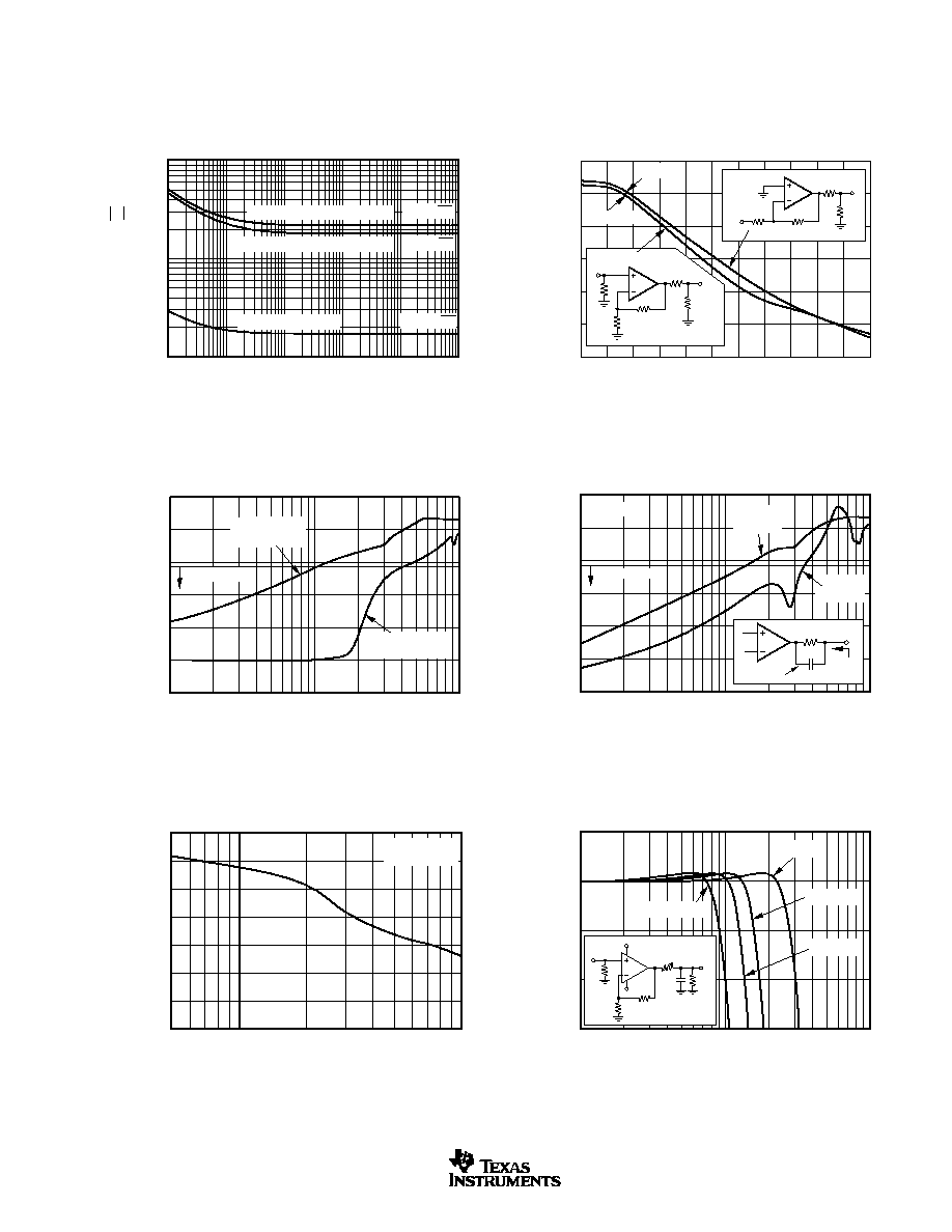
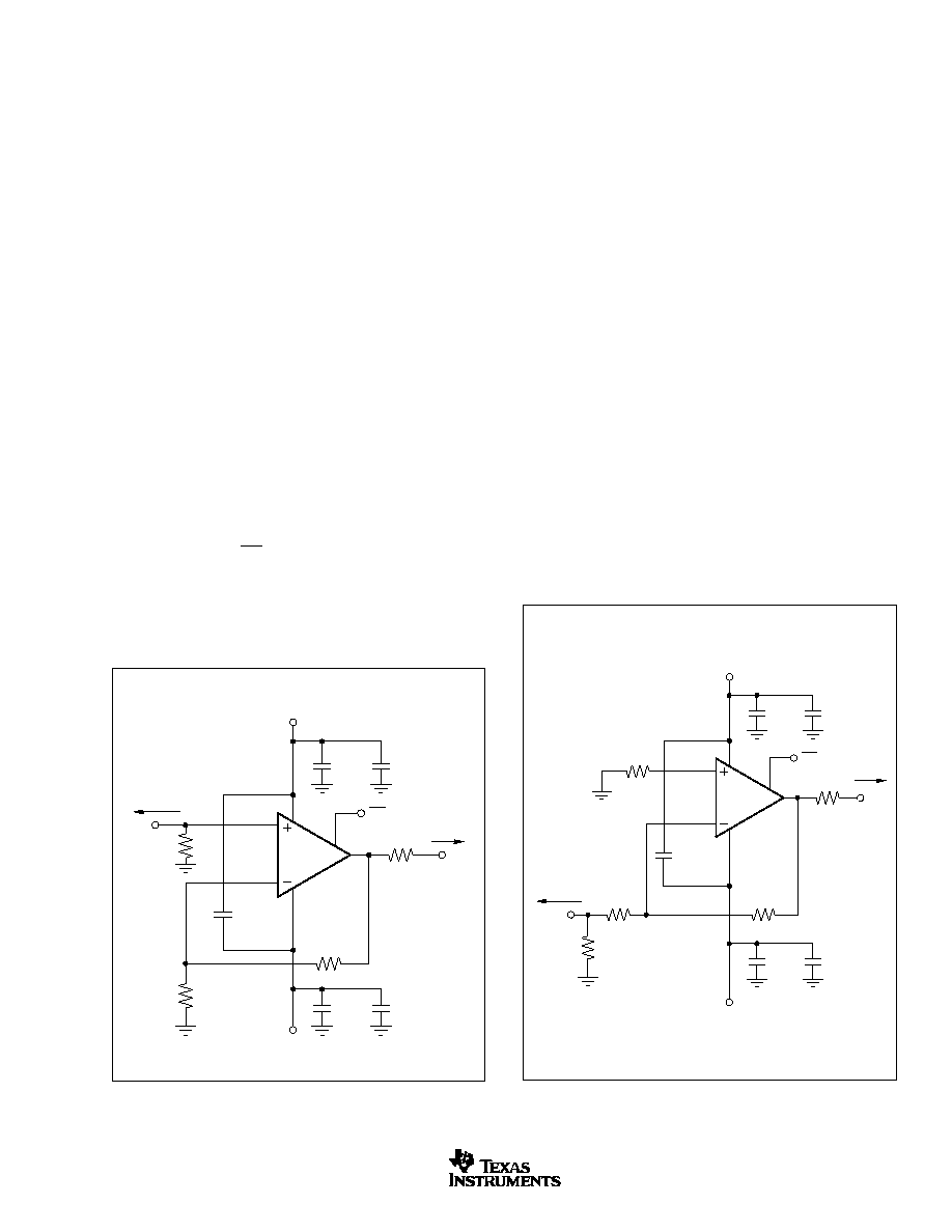
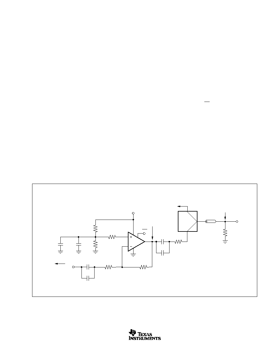
FIGURE 1. DC-Coupled, G = +8V/V, Bipolar Supply Speci-
fications and Test Circuit.
FIGURE 2. DC-Coupled, G = ≠8V/V, Bipolar Supply Speci-
fications and Test Circuit.
APPLICATIONS INFORMATION
WIDEBAND CURRENT FEEDBACK OPERATION
The OPA695 gives a new level of performance in wideband
current feedback op amps. Nearly constant AC performance
over a wide gain range, along with 4300V/
µ
s slew rate, gives
a lower power and cost solution for high-intercept IF amplifier
requirements. While optimized at a gain of +8V/V (12dB to a
matched 50
load) to give 450MHz bandwidth, applications
from gains of 1 to 40 can be supported. As a gain of +2
video line driver, the bandwidth extends to 1.4GHz with
a slew rate to support the highest pixel rates. At gains
above 20, the signal bandwidth starts to decrease, but still
exceeds 180MHz up to a gain of 40V/V (26dB to a matched
50
load). Single +5V supply operation is also supported
with similar bandwidths but reduced output power capability.
For lower speed (< 250MHz) requirements with higher output
powers, consider the OPA691.
Figure 1 shows the DC-coupled, gain of +8V/V, dual power
supply circuit used as the basis of the
±
5V Specifications and
Typical Characteristic curves. For test purposes, the input
impedance is set to 50
with a resistor to ground and the
output impedance is set to 50
with a series output resistor.
Voltage swings reported in the specifications are taken
directly at the input and output pins while load powers (dBm)
are defined at a matched 50
load. For the circuit of Figure
1, the total effective load will be 100
|| 458
= 82
. The
disable control line (DIS) is typically left open to get normal
amplifier operation. The disable line must be asserted low to
shut off the OPA695. One optional component is included in
Figure 1. In addition to the usual power supply decoupling
capacitors to ground, a 0.01
µ
F capacitor is included between
the two power supply pins. In practical PC board layouts, this
optional added capacitor will typically improve the 2nd-
harmonic distortion performance by 3dB to 6dB for bipolar
supply operation.
Figure 2 shows the DC-coupled, gain of ≠8V/V, dual power
supply circuit used as the basis of the Inverting Typical
Characteristic curves. Inverting operation offers several per-
formance benefits. Since there is no common mode signal
across the input stage, the slew rate for inverting operation
is higher and the distortion performance is slightly improved.
An additional input resistor, R
T
, is included in Figure 2 to set
the input impedance equal to 50
. The parallel combination
of R
T
and R
G
set the input impedance. Both the non-inverting
and inverting applications of Figures 1 and 2 will benefit from
optimizing the feedback resistor (R
F
) value for bandwidth
(see the discussion in
Setting Resistor Values to Optimize
Bandwidth). The typical design sequence is to select the R
F
value for best bandwidth, set R
G
for the gain, then set R
T
for
the desired input impedance. As the gain increases for the
inverting configuration, a point will be reached where R
G
will
equal 50
, where R
T
is removed and the input match is set
by R
G
only. With R
G
fixed to achieve an input match to 50
,
R
F
is simply increased, to increase gain. This will, however,
quickly reduce the achievable bandwidth, as shown by the
inverting gain of ≠16 frequency response in the Typical
Characteristic curves. For gains > 10V/V (14dB at the matched
load), noninverting operation is recommended to maintain
broader bandwidth.
OPA695
+5V
+V
S
≠V
S
DIS
≠5V
50
Load
50
20
R
T
562
R
G
54.9
+
6.8
µ
F
0.1
µ
F
+
6.8
µ
F
0.1
µ
F
Optional
0.01
µ
F
V
I
50
Source
R
F
442
V
O
OPA695
+5V
DIS
≠5V
50
Load
50
50
V
I
50
Source
R
G
56.2
R
F
402
V
O
+
6.8
µ
F
0.1
µ
F
+
6.8
µ
F
0.1
µ
F
Optional
0.01
µ
F
OPA695
14
SBOS293B
www.ti.com
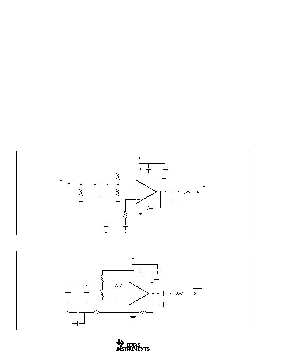
FIGURE 3. AC-Coupled, G = +8V/V, Single-Supply Specifications and Test Circuit.
FIGURE 4. AC-Coupled, G = ≠8V/V, Single-Supply Specifications and Test Circuit.
Figure 3 shows the AC-coupled, single +5V supply, gain of
+8V/V circuit configuration used as a basis for the +5V only
Specifications and Typical Characteristic curves. The key
requirement for broadband single-supply operation is to
maintain input and output signal swings within the useable
voltage ranges at both the input and the output. The circuit
of Figure 3 establishes an input midpoint bias using a simple
resistive divider from the +5V supply (two 806
resistors) to
the noninverting input. The input signal is then AC-coupled
into this midpoint voltage bias. The input voltage can swing
to within 1.6V of either supply pin, giving a 1.8V
PP
input
signal range centered between the supply pins. The input
impedance matching resistor (57.6
) used in Figure 3 is
adjusted to give a 50
input match when the parallel combi-
nation of the biasing divider network is included. The gain
resistor (R
G
) is AC-coupled, giving the circuit a DC gain of +1.
This puts the input DC bias voltage (2.5V) on the output as
well. The feedback resistor value has been adjusted from the
bipolar supply condition to re-optimize for a flat frequency
response in +5V only, gain of +8 operation (see Setting
Resistor Values to Optimize Bandwidth). On a single +5V
supply, the output voltage can swing to within 1.0V of either
supply pin while delivering more than 90mA output current
giving 3V output swing into 100
(7dBm maximum at the
matched load). The circuit of Figure 3 shows a blocking
capacitor driving into a 50
output resistor then into a 50
load. Alternatively, the blocking capacitor could be removed
with the load tied to a supply midpoint or to ground if the DC
current required by this grounded load is acceptable.
Figure 4 shows the AC-coupled, single +5V supply, gain of
≠8V/V circuit configuration used as a basis for the +5V only
Typical Characteristic curves. In this case, the midpoint DC
bias on the noninverting input is also de-coupled with an
additional 0.1
µ
F decoupling capacitor. This reduces the
source impedance at higher frequencies for the noninverting
input bias current noise. This 2.5V bias on the noninverting
input pin appears on the inverting input pin and, since R
G
is
DC blocked by the input capacitor, will also appear at the
output pin. One advantage to inverting operation is that since
there is no signal swing across the input stage, higher slew
rates and operation to even lower supply voltages are pos-
sible. To retain a 1V
PP
output capability, operation down to a
3V supply is allowed. At a +3V supply, the input common
mode range is 0V. However, for the inverting configuration of
a current feedback amplifier, wideband operation is retained
even with the input stage saturated.
OPA695
+5V
+V
S
DIS
50
Load
50
R
G
50
806
806
57.6
0.1
µ
F
1000pF
+
6.8
µ
F
0.1
µ
F
0.1
µ
F
0.1
µ
F
V
I
50
Source
R
F
348
V
O
1000pF
1000pF
OPA695
+5V
+V
S
DIS
50
Load
50
R
G
50
806
806
20
0.1
µ
F
0.1
µ
F
0.1
µ
F
V
I
R
F
400
V
O
1000pF
+
6.8
µ
F
0.1
µ
F
1000pF
1000pF

OPA695
15
SBOS293B
www.ti.com
The single-supply test circuits of Figures 3 and 4 show +5V
operation. These same circuits can be used over a single-
supply range of +5V to +12V. Operating on a single +12V
supply, with the Absolute Maximum Supply voltage specifica-
tion of +13V, gives adequate design margin for the typical
±
5% supply tolerance.
RF SPECIFICATIONS AND APPLICATIONS
The ultra-high, full-power bandwidth and 3rd-order intercept
of the OPA695 may be used to good advantage in IF
amplifier applications. Additional benefits to using a wideband
op amp such as the OPA695 include extremely good (and
independent) I/O impedance matching as well as very high
reverse isolation. A designer more accustomed to using
fixed-gain RF amplifiers will get almost perfect gain accuracy,
much higher I/O return loss, and 3rd-order intercept points
exceeding 30dBm (up to 110MHz) using only a 13mA supply
current for the OPA695. Using the considerable design
freedom achieved by adjusting the external resistors, the
OPA695 can replace a wide range of fixed-gain RF amplifiers
with a single part. To understand (in RF amplifier terms) how
to take advantage of this, consider first the 4-S parameters
(this will be done using the example circuits of Figures 1 and
2 on
±
5V supplies, but similar results can be obtained on a
single +5V to +12V supply).
INPUT RETURN LOSS (S
11
)
Input return loss is a measure of how nearly (over frequency)
the input impedance matches the source impedance. This is
relatively independent of gain setting for both the noninverting
and inverting configurations. The Typical Characteristic curves
show the magnitude of S
11
for the circuits of Figures 1 and
2 through 1GHz (noninverting gain of +8 and inverting gain
of ≠8 operation, respectively). Noninverting operation does
offer much better matching to higher frequencies, with the
only deviation due to the parasitic input capacitance of the
input pin. The noninverting input match is simply set by the
resistor to ground on the noninverting input, since the ampli-
fier itself shows a very high input impedance. Inverting
operation is also very good, but rises more quickly due to
loop gain roll-off effects appearing at the inverting node. The
inverting mode input match is set by the parallel combination
of R
G
and R
T
in Figure 2, since the inverting amplifier node
may be considered a virtual ground. A good, fixed-gain, RF
amplifier would have an input, Voltage Standing Wave Ratio
(VSWR) < 1.2:1. This corresponds to an S
11
of ≠21dB. The
OPA695 exceeds this performance through 100MHz for the
inverting mode of operation, and through 400MHz for the
noninverting mode.
OUTPUT RETURN LOSS (S
22
)
Output return loss is a measure of how nearly (over fre-
quency) the output impedance matches the load impedance.
This is relatively independent of gain setting for both the
noninverting and inverting configurations. The output match-
ing impedance, to a first order, is, simply set by adding a
series resistor to the low impedance output of the op amp.
Since the op amp itself shows a very low output impedance
that increases with frequency, an improvement in the output
match can therefore be obtained by adding a small equaliz-
ing capacitor across this output resistor. The Typical Charac-
teristic curves show the measured S
22
with and without this
2.5pF capacitor (across the 50
output resistor). Again, a
very good match for a fixed-gain RF amplifier would give a
VSWR of 1.2:1 (S
22
< ≠21dB). The Typical Characteristic
curves show the measured S
22
with and without this 2.5pF
capacitor across the 50
output resistor. The Typical Char-
acteristic curves show that a simple 50
output resistor holds
better than ≠21dB to 140MHz, but up to 380MHz with the
tuning capacitor.
FORWARD GAIN (S
21
)
In all high-speed amplifier data sheets, this is referred to as
the small signal gain which is plotted over frequency. The
difference between noninverting and inverting operation is
that the phase of S
21
starts out at 0
∞
for the noninverting and
≠180
∞
for the inverting. This initial phase shift for inverting
mode is inconsequential to most IF strip applications. The
phase of S
21
was not shown in the Typical Characteristic
curves, but is very linear with frequency and may be accu-
rately modeled as a constant time delay through the ampli-
fier.
The Typical Characteristic Curves for the OPA695 show S
21
over a range of signal gains where the external resistors
have been adjusted to re-optimize flatness at each gain
setting. Since this is a current feedback op amp, the signal
bandwidth can be held relatively constant as the desired gain
setting is changed. The plot of the noninverting bandwidth
versus gain shows some change in bandwidth versus gain
(due to parasitic capacitive effects on the inverting node) with
very little change showing up for the inverting mode of
operation.
Signal gains are most often referred to as V/V in op amp data
sheets. This is the voltage gain from input to output and is set
by external resistor ratios. Since the output impedance is set
by a physical series resistor, the voltage gain to the matched
load is cut in 1/2 by this resistor divider. The log gain to the
matched load for the noninverting circuit of Figure 1 is:
G
R
R
dB
F
G
+
=
+
20
1
2
1
log
The log gain to the matched load for the inverting circuit of
Figure 2 is:
G
R
R
dB
F
G
≠
log
=
20
1
2
The specific resistor values used in Figures 1 and 2 give both
a maximally flat bandwidth and a 12dB gain to the matched
load. The design tables at the end of this section summarize
the required resistor values over a range of desired gains for
the circuits of Figures 1 and 2.
As the desired signal gain increases, the achievable band-
widths will decrease. In the noninverting case, it decreases
relatively quickly as shown in the Typical Characteristic
(1)
(2)

OPA695
16
SBOS293B
www.ti.com
curves. The inverting configuration holds almost constant
bandwidth (with correctly selected external resistor values)
until R
G
reduces to equal 50
, and remains at that value to
satisfy the input impedance matching requirement, with fur-
ther increases in gain achieved by increasing R
F
in Figure 2.
The bandwidth then decreases rapidly as shown by the gain
of ≠16V/V plot in the Typical Characteristic curves.
REVERSE ISOLATION (S
12
)
Reverse isolation is a measure of how much power injected
into the output pin makes it back to the source. This is rarely
specified for an op amp because it is so good. Op amps are
very nearly uni-directional signal devices. Below 300MHz,
the noninverting configuration of Figure 1 gives much better
isolation than the inverting of Figure 2. Both are well below
40dB isolation through 350MHz.
LIMITS TO DYNAMIC RANGE
The next set of considerations for RF amplifier applications
are the defined limits to dynamic range. Typical fixed-gain RF
amplifiers include:
∑ ≠1dB compression (a measure of maximum output power)
∑ Two-tone, 3rd-order, output intermodulation intercept (a
measure of achievable spurious-free dynamic range)
∑ Noise figure (a measure of degradation in signal to noise
ratio in passing through the amplifier)
≠1dB COMPRESSION
The definition for ≠1dB compression power is that output
power where the actual power is 1dB less than the input
power plus the log gain. In classic RF amplifiers, this is
typically 10dB less than the 3rd-order intercept. That relation-
ship does not hold for op amps since their intercept is
considerably improved by loop gain to be far more than 10dB
higher than the ≠1dB compression. A simple estimate for
≠1dB compression for the OPA695 is the maximum non-slew
limited output voltage swing available at the matched load
converted into a power with 1dB added to satisfy the defini-
tion. For the OPA695 on
±
5V supplies, its output will deliver
approximately
±
4.0V at the output pin or
±
2.0V at the matched
load. The conversion from V
PP
to power (for a sine wave) is:
P
dBm
V
O
PP
(
)
=
(
)
10
2 2
0 001 50
2
log
.
Converting this 4.0V
PP
swing at the load to dBm gives
16dBm; adding 1dB to this (to satisfy the definition) gives a
≠1dB compression of 17dBm for the OPA695 operating on
±
5V supplies. This will be a good estimate for frequencies
that require less than the full slew rate of the OPA695.
The maximum frequency of operation given an available
slew rate and desired peak output swing (at the output pin for
a sine wave) is:
F
Slew Rate
V
MAX
p
=
2
0 707
( .
)
Putting in the 4600V/
µ
s slew rate available in the inverting
mode of operation and the 4.0V peak output swing at the
output pin gives a maximum frequency of 259MHz. This is
the maximum frequency where the ≠1dB compression would
be 17dBm at the matched load. Higher useable bandwidths
are possible at lower output powers, as shown in the Large
Signal Bandwidth curves. As those graphs show, 7V
PP
out-
puts are possible with almost perfect frequency response
flatness through 100MHz for both non-inverting or inverting
operation.
TWO-TONE 3rd-ORDER OUTPUT
INTERMODULATION INTERCEPT (OP
3
)
In narrowband IF strips, each amplifier typically feeds into a
bandpass filter that attenuates most harmonic distortion
terms. The most troublesome remaining distortion is the 3rd-
order, two-tone intermodulations that can fall very close (in
frequency) to the desired signals and cannot be filtered out.
If two test frequencies are defined at F
O
+
F and F
O
≠
F,
the 3rd-order intermodulation distortion products will fall at
F
O
+ 3
F and F
O
≠ 3
F. If the two test power levels (P
T
) are
equal, the OPA695 will produce 3rd-order spurious terms
(P
S
) that are at these frequencies and at a power level below
the test power levels given by:
P
P
OP
P
T
S
T
≠
≠
=
(
)
2
3
The 3rd-order intercept plot shown in the Typical Character-
istic curves shows a very high intercept at low frequencies
that decreases with increasing frequency. This intercept is
defined at the matched load to allow direct comparison with
fixed-gain RF amplifiers. To produce a 2V
PP
total two-tone
envelope at the matched load, each power level must be
4dBm at the matched load (1V
PP
). Using Equation 5, and the
performance curve for inverting operation, at 50MHz (41.5dBm
intercept) the 3rd-order spurious will be 2 ∑ (41.5 ≠ 4) = 75dB
below these 4dBm test tones. This is an exceptionally low
distortion for an amplifier that only uses 13mA supply current.
Considerable improvement from this level of performance is
also possible if the output drives directly into the lighter load
of an ADC input (see
High SFDR Differential ADC driver
section).
This very high intercept versus quiescent power is achieved
by the high loop gain of the OPA695. This loop gain does,
however, decrease with frequency, giving the decreasing
OP3 performance shown in the Typical Characteristics. Ap-
plication as an IF amplifier through 200MHz is possible with
output intercepts exceeding 21dBm at 200MHz. Intercept
performance will vary slightly with gain setting decreasing at
higher gains (that is, gains greater than the 8V/V, or 12dB,
gain used in the Typical Characteristic curves) and increas-
ing at lower gains.
(3)
(4)
(5)

OPA695
17
SBOS293B
www.ti.com
FIGURE 5. IF Amplifier with Improved Noise Figure.
GAIN TO LOAD
R
F
R
G
NOISE
(dB)
(
)
(
)
FIGURE
6
478
159
17.20
7
468
134
16.55
8
458
113
15.95
9
446
96
15.40
10
433
81
14.91
11
419
68
14.47
12
402
57
14.09
13
384
48
13.76
14
363
40
13.23
15
340
33
13.23
16
314
27
13.03
17
284
21
12.86
18
252
16
12.72
19
215
12
12.60
20
174
9
12.51
TABLE I. Noninverting Wideband Op Amp (Figure 1).
GAIN TO LOAD
R
F
R
G
NOISE
(dB)
(
)
(
)
FIGURE
6
516
518
16.34
7
511
412
15.54
8
506
334
14.78
9
500
275
14.07
10
493
228
13.40
11
486
190
12.78
12
478
160
12.21
13
469
135
11.70
14
458
114
11.25
15
447
96
10.85
16
434
81
10.15
17
419
69
10.21
18
403
58
9.96
19
384
48
9.74
20
364
40
9.57
TABLE II.
Noninverting with a 1:2 Input Step-Up Trans-
former (Figure 5).
GAIN TO LOAD
OPTIMUM
R
G
INPUT
NOISE
(dB)
R
F
(
)
(
)
MATCH R
T
FIGURE
6
463.27
116
87
16.94
7
454.61
101
98
16.06
8
444.91
88
114
15.16
9
434.07
77
142
14.23
10
421.95
66
199
13.24
11
408.42
57
380
12.16
12
398.11
50
Infinite
11.03
13
446.68
50
Infinite
10.92
14
501.19
50
Infinite
10.83
15
562.34
50
Infinite
10.75
16
630.96
50
Infinite
10.67
17
707.95
50
Infinite
10.61
18
794.33
50
Infinite
10.55
19
891.25
50
Infinite
10.49
20
1000.00
50
Infinite
10.45
TABLE III. Inverting Wideband RF Amplifier (Figure 2).
NOISE FIGURE
All fixed-gain RF amplifiers show a very good noise figure
(typically < 5dB). For broadband amplifiers, this is achieved
by a low-noise input transistor and an input match set by
feedback. This feedback greatly reduces the noise figure for
fixed-gain RF amplifiers, but also makes the input match
dependent on the load and the output match dependent on
the source impedance at the input.
The noise figure for an op amp is always higher than for
fixed-gain RF amplifiers due to the more complex internal
circuits of an op amp (giving higher input noise voltage and
current terms). Also, for simple circuits, the input match is set
resistively. What is gained is an almost perfect I/O imped-
ance match, much better load isolation, and very high 3rd-
order intercepts versus quiescent power. These higher noise
figures can be acceptable if the OPA695 has enough gain
preceding it in the IF chain.
Op amp noise figure equations include at least six terms (see
the Noise Performance section), due to the external resis-
tors. As a point of reference, the circuit of Figure 1 has an
input noise figure of 14dB while the inverting configuration of
Figure 2 has an input noise figure of 11dB. At higher gains,
it is typical for the inverting noise figure to be slightly better
than for an equivalent gain, noninverting configuration. One
easy way to improve the noise figure for the noninverting
configuration of the OPA695 is to include a step-up, 1:2 turns
ratio transformer at the input. This configuration is shown in
Figure 5.
OPA695
+5V
DIS
≠5V
50
Load
Supply decoupling
not shown.
50
R
G
200
V
I
V
O
R
F
50
Source
1:2
In all cases, exact computed values for resistors are shown--
in application, pick standard resistor values that are closest
to those in the tables.
The transformer provides a noiseless voltage gain at the
expense of higher source impedance for the OPA695
noninverting input current noise. The input impedance is still
set to 50
by the 200
resistor on the transformer second-
ary. A 1:2 turns ratio transformer will reflect the 200
to the
input side as a 50
impedance over the bandwidth of the
transformer. Using a 1:2 step-up transformer will also reduce
the required amplifier gain by 1/2 for any particular desired
overall gain.
Tables I - III summarize the recommended resistor values
and resulting noise figures over the desired gain setting for
three circuit options for the OPA695 operated as a precision
IF amplifier. In each case, R
F
and R
G
are adjusted for both
best bandwidth and to achieve the required gain.
OPA695
18
SBOS293B
www.ti.com
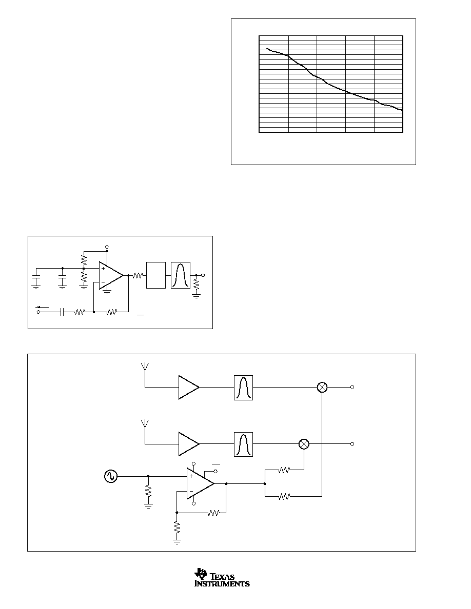
FIGURE 8. Dual Output LO Buffer.
SAW FILTER BUFFER
One common requirement in an IF strip is to buffer the output
of a mixer with enough gain to recover the insertion loss of
a narrowband SAW filter. Figure 6 shows one possible
configuration driving a SAW filter. Figure 7 shows the inter-
cept at the 50
load. Operating in the inverting mode at a
voltage gain of ≠8V/V, this circuit provides a 50
input match
using the gain set resistor, has the feedback optimized for
maximum bandwidth (700MHz in this case), and drives
through a 50
output resistor into the matching network at
the input of the SAW filter. If the SAW filter gives a 12dB
insertion loss, a net gain of 0dB to the 50
load at the output
of the SAW (which could be the input impedance of the next
IF amplifier or mixer) will be delivered in the passband of the
SAW filter. Using the OPA695 in this application will isolate
the first mixer from the impedance of the SAW filter and
provide very low two-tone, 3rd-order spurious levels in the
SAW filter bandwidth. Inverting operation will give the broad-
est bandwidth up to a gain of ≠12V/V (15.6dB). Noninverting
operation will give higher bandwidth at gain settings higher
than this, but will also give a slight reduction in intercept and
Noise Figure performance.
OPA695
R
F
511
R
G
511
50
50
LO
50
LNA
Diversity Receiver
Antenna
Antenna
IF1
IF2
Bandpass
Filter
Bandpass
Filter
LNA
≠5V
+5V
DIS
Power supply decoupling not shown.
LO BUFFER AMPLIFIER
The OPA695 may also be used to buffer the Local Oscillator
(LO) from the mixer(s). Operating at a voltage gain of +2, the
OPA695 will provide almost perfect load isolation for the LO
with a net gain of 0dB to the mixer. Applications through
1.4GHz LOs may be considered, but best operation would be
for LOs < 1.0GHz at a gain of +2. Gain could also be easily
provided by the OPA695 to drive higher power levels into the
mixer. One unique option in using the OPA695 as an LO
buffer is shown in Figure 8. Since the OPA695 can drive
multiple output loads, two identical LO signals may be
delivered to the mixers in a diversity receiver simply by
tapping the output off through two series 50
output resis-
tors. This circuit is set up for a voltage gain of +2V/V to the
output pin for a gain of +1V/V (0dB) to the mixers, but could
easily be adjusted to deliver higher gains as well.
OPA695
SAW
Filter
+12V
Matching
Network
= 12dB ≠ (SAW Loss)
50
Source
50
50
P
O
P
O
P
I
400
50
P
I
0.1
µ
F
1000pF
1000pF
5k
5k
FIGURE 6. IF Amplifier Driving SAW Filter.
FIGURE 7. 2-Tone, 3rd-Order Intermodulation Intercept.
50
40
30
20
10
Center Frequency (MHz)
0
50
150
250
200
100
Output Intercept (dBm)
OPA695
19
SBOS293B
www.ti.com
FIGURE 9. Cable Modem Upstream Driver.
WIDEBAND CABLE DRIVING
APPLICATIONS
The high slew rate and bandwidth of the OPA695 can be
used to meet the most demanding cable driving applications.
CABLE MODEM RETURN PATH DRIVER
The standard cable modem upstream driver is typically
required to drive high power over a 5MHz to 65MHz band-
width while delivering < ≠50dBc distortion. Highly-integrated
solutions (including programmable gain stages) often fall
short of this target due to high losses from the amplifier
output to the line. The higher gain operating capability of the
OPA695, along with its very high slew rate, provides a low-
cost solution for delivering this signal with the required
spurious-free dynamic range. Figure 9 shows one example
of using the OPA695 as an upstream driver for a cable
modem return path. In this case, the input impedance of the
driver is set to 75
by the gain resistor (R
G
). The required
input level from the adjustable gain stage is significantly
reduced by the 15.5dB gain provided by the OPA695. In this
example, the physical 75
output matching resistor, along
with the 3dB loss in the diplexer, will attenuate the output
swing by 9dB on the line. In this example, a single +12V
supply was used to achieve the lowest harmonic distortion
for the 6V
PP
output pin voltage through 65MHz. Measured
performance for this example gave 600MHz small-signal
bandwidth and < ≠54dBc distortion through 65MHz for a
6V
PP
output pin voltage swing.
OPA695
R
F
450
R
G
75
75
6k
6k
20
75
Diplexer
≠3dB
Receive Channel
Supply decoupling
not shown
67dBmV
+12V
PGA Output
58dBmV
0.1
µ
F
1000pF
0.01
µ
F
0.1
µ
F
51.5dBmV
DIS
1000pF
1000pF
An alternative to this circuit, giving even lower distortion, is a
differential driver using two OPA695s driving into an output
transformer. This can be used either to double the available
line power, or to improve distortion by cutting the required
output swing in half for each stage. The channel disable
required by the MCNS specification should be implemented
by using the PGA disable feature. The MCNS disable speci-
fication requires that an output impedance match be main-
tained with the signal channel shut off. The disable feature of
the OPA695 is intended principally for power savings and
puts the output and inverting input pins into a high imped-
ance mode. This will not maintain the required output imped-
ance matching. Turning off the signal at the input of Figure
9, while keeping the OPA695 active, will maintain the imped-
ance matching while putting very little noise on the line. The
line noise in disable for the circuit of Figure 9 (with the PGA
source turned off, but still presenting a 75
source imped-
ance) will be a very low 4nV/
Hz (≠157dBm/Hz) due to the
low input noise of the OPA695.
RGB VIDEO LINE DRIVER
The extremely high bandwidth of the OPA695 operating at a
gain of +2 will support the fastest RAMDAC outputs for
applications such as auxiliary monitor driving. The front page
of this data sheet shows measured performance for a
0
+1V input square wave at 125MHz. As a general rule,
the required full-power bandwidth for the amplifier must be at
least one-half the pixel rate. With its noninverting gain of +2,
slew rate of 2900V/
µ
s, and a 1.4V
PP
output pin voltage swing
for standard RGB video levels, the OPA695 will give a
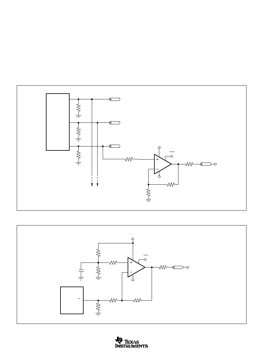
OPA695
20
SBOS293B
www.ti.com
FIGURE 11. High-Resolution RGB Driver Using DAC Complementary Output Current.
bandwidth of 600MHz, which will then support up to 1.26GHz
pixel rates. Figure 10 shows an example where three
OPA695s provide an auxiliary monitor output for a high-
resolution RGB RAMDAC.
An alternative circuit that will take advantage of the higher
inverting slew rate of the OPA695 (4300V/
µ
s) takes the
complementary current output from the RAMDAC and con-
verts it to positive video to give a very high, full-power
bandwidth RGB line driver. This will give sharper pixel edges
than the circuit of Figure 10. Most high-speed DACs are
current-steering designs where there is both an output
current signal that is used for the video, and a complemen-
OPA695
75
R
F
500
R
G
536
R
T
86.6
+5V
Power supply decoupling not shown.
≠5V
RAMDAC
768
4.22k
0.77V
20
0.1
µ
F
DIS
I
O
tary output that is typically discarded into a matching resistor.
The complementary current output can be used as an aux-
iliary output if it is inverted, as shown in Figure 11.
In the circuit of Figure 11, the complementary current output
is terminated by an equivalent 75
impedance (the parallel
combination of R
T
and R
G
) that also provides a current
division to reduce the signal current through the feedback
resistor, R
F
. This allows R
F
to be increased to a value which
will hold a flat frequency response. Since the complementary
current output is essentially an inverted video signal, this
circuit sets up a white video level at the output of the OPA695
for zero DAC output current (using the 0.77V DC bias on the
FIGURE 10. Gain of +2, High-Resolution RGB Monitor Output.
OPA695
75
75
511
R
F
511
20
+5V
Blue
≠5V
75
Green
RAMDAC
75
Red
Addtional
OPA695
Stages
DIS
Power supply decoupling not shown.
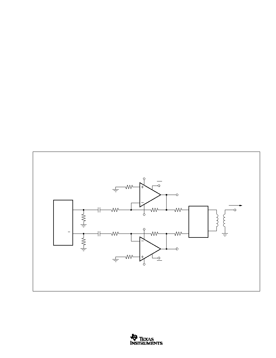
OPA695
21
SBOS293B
www.ti.com
FIGURE 12. High Power, Wideband AC-Coupled Arbitrary Waveform Driver.
OPA695
+5V
≠5V
+5V
≠5V
464
66.5
0.01
µ
F
200
20
50
OPA695
464
66.5
0.01
µ
F
200
50
DAC
20mA Peak Output
Differential
Filter
I
O
50
Source
1.4:1
±
3.5V
±
3.5V
Power supply decoupling not shown.
20
DIS
DIS
I
O
noninverting input), then inverts the complementary output
current to produce a signal that ranges from this 1.4V at zero
output current down to 0V at maximum output current level
(assuming a 20mA maximum output current). This will give a
very wideband (> 800MHz) video signal capability.
ARBITRARY WAVEFORM DRIVER
The OPA695 may be used as the output stage for moderate
output power Arbitrary Waveform Driver applications. Driving
out through a series 50
matching resistor into a 50
matched load will allow up to a 4.0V
PP
swing at the matched
load (15dBm) when operating the OPA695 on a
±
5V power
supply. This level of power is available for gains of either
±
8
with a flat response through 100MHz. When interfacing
directly from a complementary current output DAC, consider
the circuit of Figure 11, modified for the peak output currents
of the particular DAC being considered. Where purely
AC-coupled output signals are required from a complemen-
tary current output DAC, consider a push-pull output stage
using the circuit of Figure 12. The resistor values here have
been calculated for a 20mA peak output current DAC which
produces up to a 5V
PP
swing at the matched load (18dBm).
This approach will give higher power at the load with much
lower 2nd-harmonic distortion.
For a 20mA peak output current DAC, the mid-scale current
of 10mA will give a 2V DC output common-mode operating
voltage due to the 200
resistor to ground at the outputs.
The total AC impedance at each output is 50
, giving a
±
0.5V swing around this 2V common-mode voltage for the
DAC. These resistors also act as a current divider, sending
75% of the DAC output current through the feedback resistor
(464
). The blocking capacitor references the OPA695 out-
put voltage to ground, and turns the unipolar DAC output
current into a bipolar swing of 0.75 ∑ 20mA ∑ 464
= 7V
PP
at
each amplifier output. Each output is exactly 180
∞
out-of-
phase from the other, producing double 7V
PP
into the match-
ing resistors. To limit the peak output current and improve
distortion, the circuit of Figure 12 is set up with a 1.4:1 step-
down transformer. This reflects the 50
load to be 100
at
the primary side of the transformer. For the maximum 14V
PP
swing across the outputs of the two amplifiers, the matching
resistors will drop this to 7V
PP
at the input of the transformer,
then down to 5V
PP
maximum at the 50
load at the output of
the transformer. This step-down approach reduces the peak
output current to 14V
P
/(200
) = 70mA.
OPA695
22
SBOS293B
www.ti.com
DIFFERENTIAL I/O
APPLICATIONS
The OPA695 offers very low 3rd-order distortion terms with
a dominant 2nd-order distortion for the single amplifier op-
eration. For the lowest distortion, particularly where differen-
tial outputs are needed, operating two OPA695s in a differ-
ential I/O design will suppress these even-order terms, deliv-
ering extremely low harmonic distortion through high fre-
quencies and powers. Differential outputs are often preferred
for high performance ADCs, twisted-pair driving, and mixer
interfaces. Two basic approaches to differential I/Os are the
noninverting or inverting configurations. Since the output is
differential, the signal polarity is somewhat meaningless--
the noninverting and inverting terminology applies here to
where the input is brought into the two OPA695s. Each
approach has its advantages and disadvantages. Figure 13
shows a basic starting point for non-inverting differential I/O
applications.
applications to include a blocking capacitor in series with R
G
.
This reduces the gain to 1 at low frequency, rising to the A
D
expression shown above at higher frequencies. The
noninverting input approach of Figure 13 can be used for
higher gains than the inverting input approach. It will, how-
ever, have a reduced full-power bandwidth due to the lower
slew rate of the OPA695 running noninverting vs inverting
input mode of operation.
Various combinations of single-supply or AC-coupled gain
can also be delivered using the basic circuit of Figure 13.
Common-mode bias voltages on the two noninverting inputs
pass on to the output with a gain of 1, since an equal DC
voltage at each inverting node creates no current through
R
G
. This circuit does show a common-mode gain of 1 from
input to output. The source connection should either remove
this common-mode signal if undesired (using an input trans-
former can provide this function), or the common-mode
voltage at the inputs can be used to set the output common-
mode bias. If the low common-mode rejection of this circuit
is a problem, the output interface may also be used to reject
that common-mode. For instance, most modern differential
input ADCs reject common-mode signals very well, while a
line driver application through a transformer will also remove
the common-mode signal at the secondary of the trans-
former.
Figure 14 shows a differential I/O stage configured as an
inverting amplifier. In this case, the gain resistors (R
G
)
become part of the input resistance for the source. This
provides a better noise performance than the non-inverting
configuration, but does limit the flexibility in setting the input
impedance separately from the gain.
R
F
500
R
F
500
OPA695
+V
CC
≠V
CC
+V
CC
≠V
CC
R
G
V
O
OPA695
V
I
FIGURE 13. Noninverting Input Differential I/O Amplifier.
FIGURE 14. Inverting Input Differential I/O Amplifier.
R
F
500
R
F
500
R
G
R
G
OPA695
+V
CC
≠V
CC
V
CM
V
CM
≠V
CC
V
O
OPA695
V
I
This approach allows for a source termination impedance
that is independent of the signal gain. For instance, simple
differential filters may be included in the signal path right up
to the non-inverting inputs without interacting with the
gain setting. The differential signal gain for the circuit of
Figure 13 is:
A
D
= 1 + 2 ∑ R
F
/R
G
Since the OPA695 is a current feedback amplifier, its band-
width is principally controlled with the feedback resistor
value--Figure 13 shows a typical value of 500
. However,
the differential gain may be adjusted with considerable free-
dom using just the R
G
resistor. In fact, R
G
may be a reactive
network providing a very isolated shaping to the differen-
tial frequency response. It is common for AC-coupled
(6)
The two noninverting inputs provide an easy common-mode
control input. This is particularly easy if the source is AC-
coupled through either blocking caps or a transformer. In
either case, the common-mode input voltages on the two
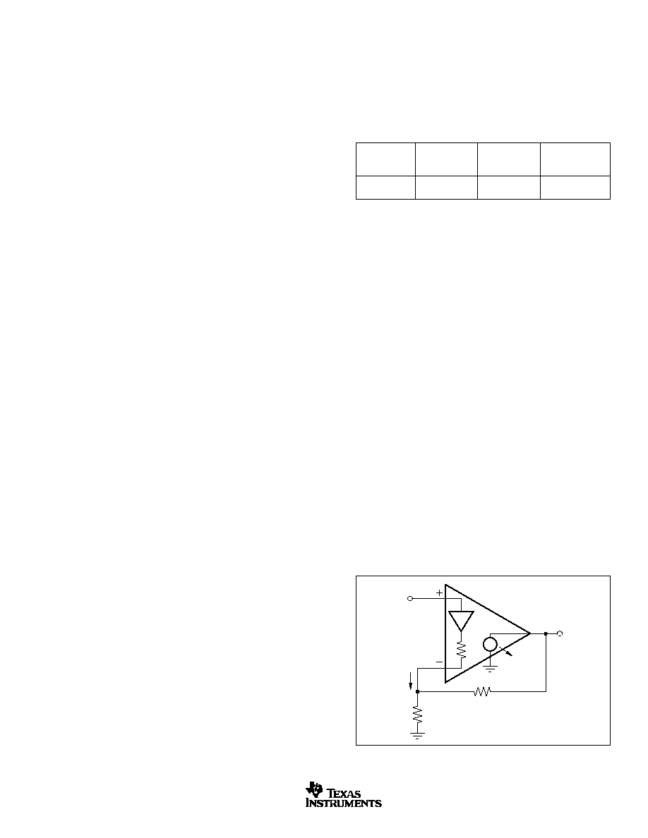
OPA695
23
SBOS293B
www.ti.com
noninverting inputs again have a gain of 1 to the output pins,
giving particularly easy common-mode control for single-
supply operation. The OPA695 used in this configuration
does constrain the feedback to the 500
region for best
frequency response. With R
F
fixed, the input resistors may be
adjusted to the desired gain, but will also be changing the
input impedance as well. The high-frequency common-mode
gain for this circuit from input to output will be the same as
for the signal gain. Again, if the source might include an
undesired common-mode signal, that could be rejected at
the input using blocking caps (for low-frequency and DC
common-mode) or a transformer coupling. The differential
performance plots shown in the Typical Characteristics used
the configuration of Figure 14 and an input 1:1 transformer.
The differential signal gain in the circuit of Figure 14 is:
A
D
= R
F
/R
G
Using this configuration suppresses the 2nd-harmonics, leav-
ing only 3rd-harmonic terms as the limit to output SFDR. The
much higher slew rate of the inverting configuration also
extends the full-power bandwidth and the range of very low
intermodulation distortion over the performance bandwidth
available from the circuit of Figure 13. The Typical Charac-
teristics show that the circuit of Figure 14 operating at an
A
D
= 10 can deliver a 16V
PP
signal with over 500MHz ≠3dB
bandwidth. Using Equation 4, this implies a differential output
slew of 18000V/
µ
sec, or 9000V/
µ
sec at each output. This
output slew rate is far higher than specified, and probably
due to the lighter load used in the differential tests.
This inverting input differential configuration is particularly
suited to very high SFDR converter interfaces--specifically
narrowband IF channels. The Typical Characteristics show
the 2-tone, 3rd-order intermodulation intercept exceeding
45dBm through 90MHz. Although this data was taken with an
800
load, the intercept model appears to work for this
circuit, simply treating the power level as if it were into 50
.
For example, at 70MHz, the differential Typical Characteristic
plots show a 48dBm intercept. To predict the 2-tone
intermodulation SFDR, assuming a ≠1dB below full-scale
envelope to a 2V
PP
maximum differential input converter, the
test power level would be 9dBm ≠ 6dBm = 3dBm for each
tone. Putting this into the intercept equation, gives:
dBc = 2 ∑ (48 ≠ 3) = 90dBc
The single-tone distortion data shows approximately 72dB
SFDR at 70MHz for a 2V
PP
output into this light 800
load.
A modest post filter after the amplifier can reduce these
harmonics (2nd at 140MHz, 3rd at 210MHz) to the point
where the full SFDR to a converter can be in the 85dB range
for a 70MHz IF operation.
FIGURE 15. Current-Feedback Transfer Function Analysis
Circuit.
R
F
V
O
R
G
R
I
Z
(S)
i
ERR
i
ERR
V
I
BOARD
LITERATURE
PART
REQUEST
PRODUCT
PACKAGE
NUMBER
NUMBER
OPA695ID
SO-8
DEM-OPA68xU
MKT-351
OPA691IDBV
SOT23-6
DEM-OPA6xxN
MKT-348
DESIGN-IN TOOLS
DEMONSTRATION BOARDS
Two PC boards are available to assist in the initial evaluation
of circuit performance using the OPA695 in its two package
styles. Both of these are available free, as unpopulated PC
boards delivered with descriptive documentation. The sum-
mary information for these boards is shown below.
The board can be requested through the Texas Instruments
web site (www.ti.com).
OPERATING SUGGESTIONS
SETTING RESISTOR VALUES TO OPTIMIZE
BANDWIDTH
A current-feedback op amp such as the OPA695 can hold an
almost constant bandwidth over signal gain settings with the
proper adjustment of the external resistor values. This is
shown in the Typical Characteristic curves. The small-signal
bandwidth decreases only slightly with increasing gain. These
curves also show that the feedback resistor has been changed
for each gain setting. The resistor
values on the inverting
side of the circuit for a current-feedback op amp can be
treated as frequency response compensation elements while
their
ratios set the signal gain. Figure 15 shows the analysis
circuit for the OPA695 small-signal frequency response.
The key elements of this current feedback op amp model are:
Buffer gain from the noninverting input to the invert-
ing input
R
I
Buffer output impedance
i
ERR
Feedback error current signal
Z(s)
Frequency-dependent, open-loop transimpedance
gain from i
ERR
to V
O
(7)
(8)
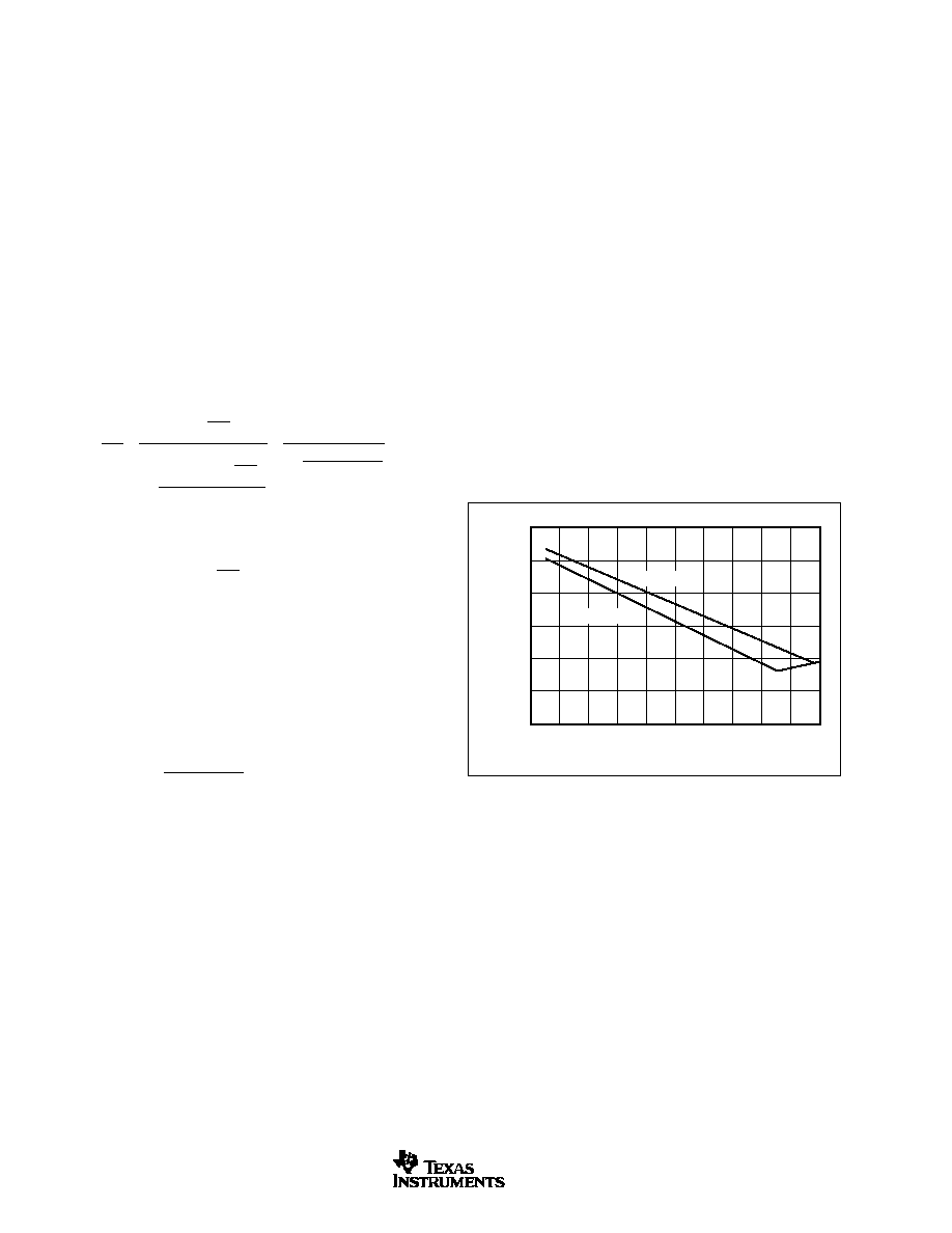
OPA695
24
SBOS293B
www.ti.com
FIGURE 16. Recommended Feedback Resistor vs Noise
Gain.
600
500
400
300
200
100
0
0
2
4
6
8
10
12
14
16
18
20
Noise Gain (V/V)
Feedback Resistor (
)
V
S
= +5V
V
S
=
±
5V
The buffer gain is typically very close to 1.00 and is normally
neglected from signal gain considerations. It will, however,
set the CMRR for a single op amp differential amplifier
configuration. For the buffer gain
< 1.0, the CMRR =
≠20 ∑ log (1 ≠
).
R
I
, the buffer output impedance, is a critical portion of the
bandwidth control equation. For the OPA695, it is typically
about 28
for
±
5V operation and 31
for single +5V opera-
tion.
A current-feedback op amp senses an error current in the
inverting node (as opposed to a differential input error volt-
age for a voltage-feedback op amp) and passes this on to the
output through an internal frequency-dependent
transimpedance gain. The Typical Characteristic curves show
this open-loop transimpedance response. This is analogous
to the open-loop voltage gain curve for a voltage-feedback
op amp. Developing the transfer function for the circuit of
Figure 18 gives Equation 9:
V
V
R
R
R
R
R
R
Z
NG
R
R
NG
Z
O
I
F
G
F
I
F
G
S
F
I
S
=
+
+
+
+
=
∑
+
+
∑
1
1
1
1
( )
( )
Where
NC
R
R
Noise Gain
F
G
= +
=
1
This is written in a loop gain analysis format, where the errors
arising from a non-infinite open-loop gain are shown in the
denominator. If Z(s) were infinite over all frequencies, the
denominator of Equation 9 would reduce to 1, and the ideal
desired signal gain shown in the numerator would be achieved.
The fraction in the denominator of Equation 9 determines the
frequency response. Equation 10 shows this as the loop gain
equation:
Z
R
R
NG
Loop Gain
S
F
I
( )
+
∑
=
If 20 ∑ log (R
F
+ NG ∑ R
I
) were superimposed on the open-
loop transimpedance plot, the difference between the two
would be the loop gain at a given frequency. Eventually, Z(s)
rolls off to equal the denominator of Equation 10, at which
point the loop gain has reduced to 1 (and the curves have
intersected). This point of equality is where the amplifier
closed-loop frequency response given by Equation 9 will
start to roll off, and is exactly analogous to the frequency at
which the noise gain equals the open-loop voltage gain for a
voltage-feedback op amp. The difference here is that the
total impedance in the denominator of Equation 10 may be
controlled separately from the desired signal gain (or NG).
The OPA695 is internally compensated to give a maximally
flat frequency response for R
F
= 402
at NG = 8 on
±
5V
supplies. Evaluating the denominator of Equation 7 (which is
the feedback transimpedance) gives an optimal target of
663
. As the signal gain changes, the contribution of the
NG ∑ R
I
term in the feedback transimpedance will change, but
the total can be held constant by adjusting R
F
. Equation 11
gives an approximate equation for optimum R
F
over signal
gain:
R
NG R
F
I
=
∑
663
≠
As the desired signal gain increases, this equation will
eventually predict a negative R
F
. A somewhat subjective limit
to this adjustment can also be set by holding R
G
to a
minimum value of 10
. Lower values will load both the buffer
stage at the input and the output stage if R
F
gets too low,
actually decreasing the bandwidth. Figure 16 shows the
recommended R
F
versus NG for both
±
5V and a single +5V
operation. The optimum target feedback impedance for +5V
operation used in Equation 8 is 663
, while the typical buffer
output impedance is 32
. The values for R
F
versus gain
shown here are approximately equal to the values used to
generate the Typical Characteristic curves. In some cases,
the values used differ slightly from that shown here, in that
the values used in the Typical Characteristics are also
correcting for board parasitics not considered in the simpli-
fied analysis leading to Equation 11. The values shown in
Figure 16 give a good starting point for designs where
bandwidth optimization is desired and a flat frequency re-
sponse is needed.
(9)
(10)
The total impedance presented to the inverting input may be
used to adjust the closed-loop signal bandwidth. Inserting a
series resistor between the inverting input and the summing
junction will increase the feedback impedance (denominator
of Equation 10), decreasing the bandwidth. The internal
buffer output impedance for the OPA695 is slightly influ-
enced by the source impedance looking out of the non-
inverting input terminal. High source resistors will have the
effect of increasing R
I
, decreasing the bandwidth. For those
single-supply applications which develop a midpoint bias at
the non-inverting input through high-valued resistors, the
decoupling capacitor is essential for power-supply ripple
rejection, non-inverting input noise current shunting, and
minimizing the high-frequency value for R
I
in Figure 15.
(11)

OPA695
25
SBOS293B
www.ti.com
Inverting feedback optimization is somewhat complicated by
the impedance matching requirement at the input, as shown
in Figure 2. The resistor values shown in Table III should be
used in this case.
OUTPUT CURRENT AND VOLTAGE
The OPA695 provides output voltage and current capabilities
that are consistent with driving doubly-terminated 50
lines.
For a 100
load at a gain of +8 (see Figure 1), the total load
is the parallel combination of the 100
load and the 456
total feedback network impedance. This 82
load will require
no more than 45mA output current to support the
±
3.7V
minimum output voltage swing specified for 100
loads. This
is well below the minimum
±
90mA specifications.
The specifications described above, though familiar in the
industry, consider voltage and current limits separately. In
many applications, it is the voltage ∑ current, or V-I, product
which is more relevant to circuit operation. Refer to the
Output Voltage and Current Limitations plot in the Typical
Characteristic curves. The X and Y axes of this graph show
the zero-voltage output current limit and the zero-current
output voltage limit, respectively. The four quadrants provide
a more detailed view of the OPA695 output drive capabilities.
Superimposing resistor load lines onto the plot shows the
available output voltage and current for specific loads.
The minimum specified output voltage and current over-
temperature are set by worst-case simulations at the cold
temperature extreme. Only at cold startup will the output
current and voltage decrease to the numbers shown in the
specification tables. As the output transistors deliver power,
the junction temperatures will increase, decreasing the V
BE
s
(increasing the available output voltage swing) and increas-
ing the current gains (increasing the available output cur-
rent). In steady-state operation, the available output voltage
and current will always be greater than that shown in the
over-temperature specifications, since the output stage junc-
tion temperatures will be higher than the minimum specified
operating ambient.
To maintain maximum output stage linearity, no output short-
circuit protection is provided. This will not normally be a
problem, since most applications include a series-matching
resistor at the output that will limit the internal power dissipa-
tion if the output side of this resistor is shorted to ground.
However, shorting the output pin directly to the adjacent
positive power supply pin will, in most cases, destroy the
amplifier. If additional short-circuit protection is required,
consider a small series resistor in the power-supply leads.
Under heavy output loads, this will reduce the available
output voltage swing. A 5
series resistor in each power-
supply lead will limit the internal power dissipation to less
than 1W for an output short circuit while decreasing the
available output voltage swing only 0.25V for up to 50mA
desired load currents. Always place the 0.1
µ
F power supply
decoupling capacitors directly on the supply pins after these
supply current-limiting resistors.
DRIVING CAPACITIVE LOADS
One of the most demanding, and yet very common, load
conditions for an op amp is capacitive loading. Often, the
capacitive load is the input of an A/D converter--including
additional external capacitance which may be recommended
to improve A/D linearity. A high-speed, high open-loop gain
amplifier like the OPA695 can be very susceptible to de-
creased stability and closed-loop response peaking when a
capacitive load is placed directly on the output pin. When the
amplifier's open-loop output resistance is considered, this
capacitive load introduces an additional pole in the signal
path that can decrease the phase margin. Several external
solutions to this problem have been suggested. When the
primary considerations are frequency response flatness, pulse
response fidelity and/or distortion, the simplest and most
effective solution is to isolate the capacitive load from the
feedback loop by inserting a series isolation resistor between
the amplifier output and the capacitive load. This does not
eliminate the pole from the loop response, but rather shifts it
and adds a zero at a higher frequency. The additional zero
acts to cancel the phase lag from the capacitive load pole,
thus increasing the phase margin and improving stability.
The Typical Characteristics show the recommended R
S
ver-
sus capacitive load and the resulting frequency response at
the load. Parasitic capacitive loads greater than 2pF can
begin to degrade the performance of the OPA695. Long PC
board traces, unmatched cables, and connections to multiple
devices can easily cause this value to be exceeded. Always
consider this effect carefully and add the recommended
series resistor as close as possible to the OPA695 output pin
(see
Board Layout Guidelines).
DISTORTION PERFORMANCE
The OPA695 provides good distortion performance into a
100
load on
±
5V supplies. Relative to alternative solutions,
the OPA695 holds much lower distortion at higher frequen-
cies (> 20MHz). Generally, until the fundamental signal
reaches very high frequency or power levels, the 2nd-
harmonic will dominate the distortion with a negligible 3rd-
harmonic component. Focusing then on the 2nd-harmonic,
increasing the load impedance improves distortion directly.
Remember, the total load includes the feedback network. In
the non-inverting configuration (Figure 1), this is the sum of
R
F
+ R
G
, while in the inverting configuration, it is just R
F
. Also,
providing an additional supply decoupling capacitor (0.01
µ
F)
between the supply pins (for bipolar operation) improves the
2nd-order distortion slightly (3dB to 6dB).
In most op amps, increasing the output voltage swing in-
creases harmonic distortion directly. The Typical Perfor-
mance Curves show the 2nd-harmonic increasing at a little
less than the expected 2x rate, while the 3rd-harmonic
increases at a little less than the expected 3x rate. Where the
test power doubles, the difference between it and the 2nd
harmonic decreases less than the expected 6dB, while the
difference between it and the 3rd decreases by less than the
expected 12dB.
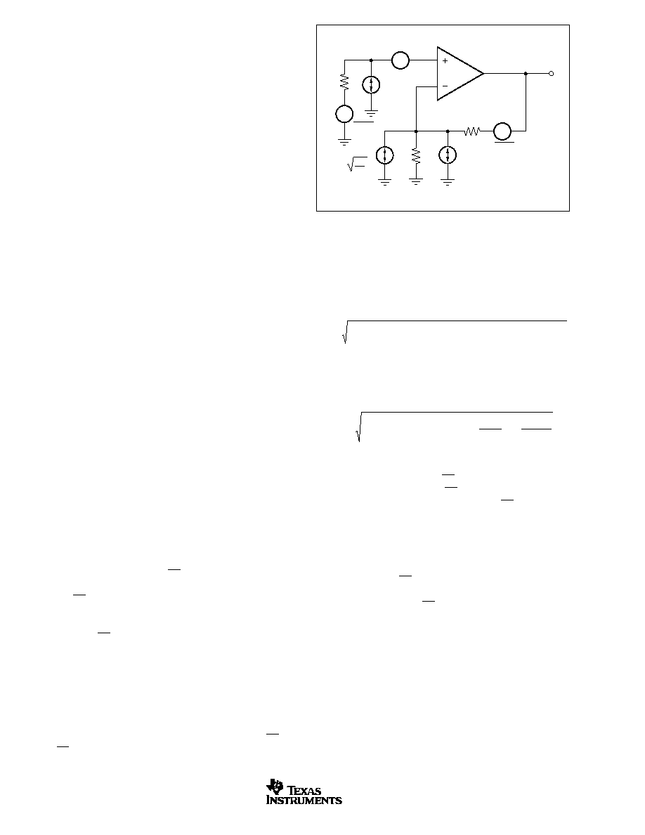
OPA695
26
SBOS293B
www.ti.com
FIGURE 17. Op Amp Noise Figure Analysis Model.
4kT
R
G
R
G
R
F
R
S
OPA695
I
BI
E
O
I
BN
4kT = 1.6E ≠20J
at 290
∞
K
E
RS
E
NI
4kTR
S
4kTR
F
The OPA695 has extremely low 3rd-order harmonic distor-
tion. This also gives a high 2-tone, 3rd-order intermodulation
intercept, as shown in the Typical Characteristic curves. This
intercept curve is defined at the 50
load when driven
through a 50
matching resistor to allow direct comparisons
to RF MMIC devices and is shown for both gains of
±
8. There
is a slight improvement in intercept by operating the OPA695
in the inverting mode. The output matching resistor attenu-
ates the voltage swing from the output pin to the load by 6dB.
If the OPA695 drives directly into the input of a high imped-
ance device, such as an ADC, this 6dB attenuation is not
taken. Under these conditions, the intercept will increase by
a minimum 6dBm.
The intercept is used to predict the intermodulation products
for two closely-spaced frequencies. If the two test frequen-
cies, F
1
and F
2
, are specified in terms of average and delta
frequency, F
O
= (F
1
+ F
2
)/ 2 and
F = | F
2
≠ F
1
| /2, the two 3rd-
order, close-in spurious tones will appear at F
O
±
3 ∑
F. The
difference between two equal test-tone power levels and
these intermodulation spurious power levels is given by
dBc = 2 ∑ (OP
3
≠ P
O
), where OP
3
is the intercept taken from
the Typical Characteristic curve and P
O
is the power level in
dBm at the 50
load for one of the two closely-spaced test
frequencies. For example, at 50MHz, gain of ≠8, the OPA695
has an intercept of 42dBm at a matched 50
load. If the full
envelope of the two frequencies needs to be 2V
PP
, this
requires each tone to be 4dBm. The 3rd-order intermodulation
spurious tones will then be 2 ∑ (42 ≠ 4) = 76dBc below the
test-tone power level (≠72dBm). If this same 2V
PP
2-tone
envelope were delivered directly into the input of an ADC
without the matching loss or the loading of the 50
network,
the intercept would increase to at least 48dBm. With the
same signal and gain conditions, but now driving directly into
a light load, the 3rd-order spurious tones will then be at least
2 ∑ (48 ≠ 4) = 88dBc below the 4dBm test-tone power levels
centered on 50MHz. Tests have shown that, in reality, the
3rd-order spurious levels are much lower due to the lighter
loading presented by most ADCs.
NOISE PERFORMANCE
The OPA695 offers an excellent balance between voltage
and current noise terms to achieve low output noise. The
inverting current noise (22pA/
Hz) is lower than most other
current-feedback op amps while the input voltage noise
(1.8nV/
Hz) is lower than any unity-gain stable, wideband,
voltage-feedback op amp. This low-input voltage noise was
achieved at the price of a higher noninverting input current
noise (18pA/
Hz). As long as the AC source impedance
looking out of the noninverting node is less than 50
, this
current noise will not contribute significantly to the total
output noise. The op amp input voltage noise and the two
input current noise terms combine to give low output noise
under a wide variety of operating conditions. Figure 17
shows the op amp noise analysis model with all the noise
terms included. In this model, all noise terms are taken to
be noise voltage or current density terms in either nV/
Hz or
pA/
Hz.
The total output spot-noise voltage can be computed as the
square root of the sum of all squared output noise voltage
contributors. Equation 12 shows the general form for the
output noise voltage using the terms shown in Figure 13.
(12)
E
E
I
R
kTR
G
I R
kTR G
O
NI
BN S
S
N
BI F
F
N
=
+
(
)
+
+
(
)
+
2
2
2
2
4
4
Dividing this expression by the noise gain (NG = (1+R
F
/R
G
))
will give the equivalent input referred spot-noise voltage at
the noninverting input as shown in Equation 13:
(13)
E
E
I
R
kTR
I R
NG
kTR
NG
N
NI
BN S
S
BI F
F
=
+
(
)
+
+
+
2
2
2
4
4
Evaluating these two equations for the OPA695 circuit and
component values shown in Figure 1 will give a total output
spot-noise voltage of 18.7nV/
Hz and a total equivalent input
spot-noise voltage of 2.3nV/
Hz. This total input referred
spot-noise voltage is higher than the 1.8nV/
Hz specification
for the op amp voltage noise alone. This reflects the noise
added to the output by the inverting current noise times the
feedback resistor. If the feedback resistor is reduced in high-
gain configurations (as suggested previously), the total input
referred voltage noise given by Equation 13 will just ap-
proach the 1.8nV/
Hz of the op amp itself. For example,
going to a gain of +20 (using R
F
= 200
) will give a total input
referred noise of 2.0nV/
Hz.
For a more complete discussion of op amp noise calculation,
see TI Application Note, SBOA066,
Noise Analysis for High
Speed Op Amps, available through the TI web site.
DC ACCURACY AND OFFSET CONTROL
A current-feedback op amp like the OPA695 provides excep-
tional bandwidth in high gains, giving fast pulse settling but
only moderate DC accuracy. The typical specifications show
an input offset voltage comparable to high-speed voltage-
feedback amplifiers; however, the two input bias currents are

OPA695
27
SBOS293B
www.ti.com
somewhat higher and are unmatched. Although bias current
cancellation techniques are very effective with most voltage-
feedback op amps, they do not generally reduce the output
DC offset for wideband current-feedback op amps. Since the
two input bias currents are unrelated in both magnitude and
polarity, matching the source impedance looking out of each
input to reduce their error contribution to the output is
ineffective. Evaluating the configuration of Figure 1, using a
worst-case +25
∞
C input offset voltage and the two input bias
currents, gives a worst-case output offset range equal to:
±
(NG ∑ V
OS
) + (I
BN
∑ R
S
/2 ∑ NG)
±
(I
BI
∑ R
F
)
where NG = non-inverting signal gain
=
±
(8 ∑ 3.0mV)
±
(30
µ
A ∑ 25
∑ 8)
±
(402
∑ 60
µ
A)
=
±
24mV
±
1.6mV
±
24mV
=
±
54mV
A fine-scale output offset null, or DC operating point adjust-
ment, is often required. Numerous techniques are available
for introducing DC offset control into an op amp circuit. Most
simple adjustment techniques do not correct for temperature
drift.
POWER SHUTDOWN OPERATION
The OPA695 provides an optional power shutdown feature
that can be used to reduce system power. If the V
DIS
control
pin is left unconnected, the OPA695 operates normally. This
shutdown is intended only as a power-saving feature. For-
ward path isolation is very good for small signals. Large
signal isolation is not ensured. Using this feature to multiplex
two or more outputs together is not recommended. Large
signals applied to the shutdown output stages can turn on
parasitic devices, degrading signal linearity for the desired
channel.
Turn-on time is very quick from the shutdown condition,
typically < 60ns. Turn-off time is strongly dependent on the
external circuit configuration, but is typically 200ns for the
circuit of Figure 1.
To shut down, the control pin must be asserted low. This
logic control is referenced to the positive supply, as shown in
the simplified circuit of Figure 18.
In normal operation, base current to Q1 is provided through
the 120k
resistor, while the emitter current through the 8k
resistor sets up a voltage drop that is inadequate to turn on
the two diodes in Q1's emitter. As V
DIS
is pulled low,
additional current is pulled through the 8k
resistor, eventu-
ally turning on these two diodes (
180
µ
A). At this point, any
further current pulled out of V
DIS
goes through those diodes
holding the emitter-base voltage of Q1 at approximately 0V.
This shuts off the collector current out of Q1, turning the
amplifier off. The supply current in the shutdown mode is only
that required to operate the circuit of Figure 18.
When disabled, the output and input nodes go to a high
impedance state. If the OPA695 is operating in a gain of +1,
this will show a very high impedance (3pF || 1M
) at the
output and exceptional signal isolation. If operating at a gain
greater than +1, the total feedback network resistance (R
F
+
R
G
) will appear as the impedance looking back into the
output, but the circuit will still show very high forward and
reverse isolation. If configured as an inverting amplifier, the
input and output will be connected through the feedback
network resistance (R
F
+ R
G
), giving relatively poor input to
output isolation.
THERMAL ANALYSIS
The OPA695 does not require external heatsinking for most
applications. Maximum desired junction temperature will set
the maximum allowed internal power dissipation as de-
scribed below. In no case should the maximum junction
temperature be allowed to exceed 150
∞
C.
Operating junction temperature (T
J
) is given by T
A
+ P
D
∑
JA
.
The total internal power dissipation (P
D
) is the sum of
quiescent power (P
DQ
) and additional power dissipated in the
output stage (P
DL
) to deliver load power. Quiescent power is
simply the specified no-load supply current times the total
supply voltage across the part. P
DL
will depend on the
required output signal and load. However, for a grounded
resistive load, P
DL
would be at a maximum when the
output is fixed at a voltage equal to one-half of either supply
voltage (for equal bipolar supplies). Under this condition,
P
DL
= V
S
2
/(4 ∑ R
L
), where R
L
includes feedback network
loading.
Note that it is the power in the output stage and not into the
load that determines internal power dissipation.
As an absolute worst-case example, compute the maximum
T
J
using an OPA695IDBV (SOT23-6 package) in the circuit
of Figure 1 operating at the maximum specified ambient
temperature of +85
∞
C and driving a grounded 100
load.
P
D
= 10V ∑ 14.1mA + 5
2
/(4 ∑ (100
|| 458
)) = 217mW
Maximum T
J
= +85
∞
C + (0.22W ∑ 150
∞
C/W) = 118
∞
C
This maximum operating junction temperature is well below
most system level targets. Most applications will be lower
since an absolute worst-case output stage power was as-
sumed in this calculation.
FIGURE 18. Op Amp Noise Figure Analysis Model.
17k
120k
8k
I
S
Control
≠V
S
+V
S
V
DIS
Q1

OPA695
28
SBOS293B
www.ti.com
BOARD LAYOUT GUIDELINES
Achieving optimum performance with a high-frequency am-
plifier like the OPA695 requires careful attention to board
layout parasitics and external component types. Recommen-
dations that will optimize performance include:
a) Minimize parasitic capacitance to any AC ground for
all of the signal I/O pins. Parasitic capacitance on the
output and inverting input pins can cause instability; on
the non-inverting input, it can react with the source imped-
ance to cause unintentional bandlimiting. To reduce un-
wanted capacitance, a window around the signal I/O pins
should be opened in all of the ground and power planes
around those pins. Otherwise, ground and power planes
should be unbroken elsewhere on the board.
b) Minimize the distance (< 0.25") from the power supply
pins to high frequency 0.1
µ
F decoupling capacitors.
At the device pins, the ground and power plane layout
should not be in close proximity to the signal I/O pins.
Avoid narrow power and ground traces to minimize induc-
tance between the pins and the decoupling capacitors.
The power-supply connections should always be decoupled
with these capacitors. An optional supply-decoupling ca-
pacitor across the two power supplies (for bipolar opera-
tion) will improve 2nd-harmonic distortion performance.
Larger (2.2
µ
F to 6.8
µ
F) decoupling capacitors, effective at
a lower frequency, should also be used on the main
supply pins. These may be placed somewhat farther from
the device and may be shared among several devices in
the same area of the PC board.
c) Careful selection and placement of external compo-
nents will preserve the high frequency performance
of the OPA695. Resistors should be a very low reactance
type. Surface-mount resistors work best and allow a
tighter overall layout. Metal-film and carbon composition,
axially-leaded resistors can also provide good high fre-
quency performance. Again, keep their leads and PC
board trace length as short as possible. Never use
wirewound-type resistors in a high frequency application.
Since the output pin and inverting input pin are the most
sensitive to parasitic capacitance, always position the
feedback and series output resistor, if any, as close as
possible to the output pin. Other network components,
such as noninverting input termination resistors, should
also be placed close to the package. Where double-side
component mounting is allowed, place the feedback resis-
tor directly under the package on the other side of the
board between the output and inverting input pins. The
frequency response is primarily determined by the feed-
back resistor value, as described previously. Increasing
its value will reduce the bandwidth, while decreasing it will
give a more peaked frequency response. The 402
feedback resistor (used in the typical performance speci-
fications at a gain of +8 on
±
5V supplies) is a good starting
point for design. Note that a 523
feedback resistor,
rather than a direct short, is required for the unity gain
follower application. A current-feedback op amp requires
a feedback resistor--even in the unity gain follower con-
figuration--to control stability.
d) Connections to other wideband devices on the board
may be made with short direct traces or through on-
board transmission lines. For short connections, con-
sider the trace and the input to the next device as a
lumped capacitive load. Relatively wide traces (50mils to
100mils) should be used, preferably with ground and
power planes opened up around them. Estimate the total
capacitive load and set R
S
from the plot of
Recommended
R
S
vs Capacitive Load. Low parasitic capacitive loads
(< 5pF) may not need an R
S
since the OPA695 is
nominally compensated to operate with a 2pF parasitic
load. If a long trace is required, and the 6dB signal loss
intrinsic to a doubly-terminated transmission line is ac-
ceptable, implement a matched impedance transmission
line using microstrip or stripline techniques (consult an
ECL design handbook for microstrip and stripline layout
techniques). A 50
environment is usually not necessary
on board. In fact, a higher impedance environment will
improve distortion, as shown in the distortion versus load
plots. With a characteristic board trace impedance de-
fined (based on board material and trace dimensions), a
matching series resistor into the trace from the output of
the OPA695 is used. A terminating shunt resistor at the
input of the destination device is used as well. Remember
also that the terminating impedance will be the parallel
combination of the shunt resistor and the input impedance
of the destination device; this total effective impedance
should be set to match the trace impedance. The high
output voltage and current capability of the OPA695
allows multiple destination devices to be handled as
separate transmission lines, each with their own series
and shunt terminations. If the 6dB attenuation of a doubly-
terminated transmission line is unacceptable, a long trace
can be series-terminated at the source end only. Treat the
trace as a capacitive load in this case and set the series
resistor value as shown in the plot of
R
S
vs Capacitive
Load. This will not preserve signal integrity as well as a
doubly-terminated line. If the input impedance of the
destination device is low, there will be some signal attenu-
ation due to the voltage divider formed by the series
output into the terminating impedance.
e) Socketing a high-speed part like the OPA695 is not
recommended. The additional lead length and pin-to-pin
capacitance introduced by the socket can create an ex-
tremely troublesome parasitic network which can make it
almost impossible to achieve a smooth, stable frequency
response. Best results are obtained by soldering the
OPA695 directly onto the board.

OPA695
29
SBOS293B
www.ti.com
FIGURE 19. Internal ESD Protection.
External
Pin
+V
CC
≠V
CC
Internal
Circuitry
INPUT AND ESD PROTECTION
The OPA695 is built using a very high-speed, complemen-
tary bipolar process. The internal junction breakdown volt-
ages are relatively low for these very small geometry de-
vices. These breakdowns are reflected in the Absolute Maxi-
mum Ratings table where an absolute maximum
±
6.5V
supply is reported. All device pins have limited ESD protec-
tion using internal diodes to the power supplies, as shown in
Figure 19.
These diodes also provide moderate protection to input
overdrive voltages above the supplies. The protection diodes
can typically support 30mA continuous current. Where higher
currents are possible (for example, in systems with
±
15V
supply parts driving into the OPA695), current-limiting series
resistors should be added into the two inputs. Keep these
resistor values as low as possible since high values degrade
both noise performance and frequency response.
OPA695
30
SBOS293B
www.ti.com
MSOI002B ≠ JANUARY 1995 ≠ REVISED SEPTEMBER 2001
D (R-PDSO-G**)
PLASTIC SMALL-OUTLINE PACKAGE
8 PINS SHOWN
8
0.197
(5,00)
A MAX
A MIN
(4,80)
0.189
0.337
(8,55)
(8,75)
0.344
14
0.386
(9,80)
(10,00)
0.394
16
DIM
PINS **
4040047/E 09/01
0.069 (1,75) MAX
Seating Plane
0.004 (0,10)
0.010 (0,25)
0.010 (0,25)
0.016 (0,40)
0.044 (1,12)
0.244 (6,20)
0.228 (5,80)
0.020 (0,51)
0.014 (0,35)
1
4
8
5
0.150 (3,81)
0.157 (4,00)
0.008 (0,20) NOM
0
∞
≠ 8
∞
Gage Plane
A
0.004 (0,10)
0.010 (0,25)
0.050 (1,27)
NOTES: A. All linear dimensions are in inches (millimeters).
B. This drawing is subject to change without notice.
C. Body dimensions do not include mold flash or protrusion, not to exceed 0.006 (0,15).
D. Falls within JEDEC MS-012
PACKAGE DRAWINGS
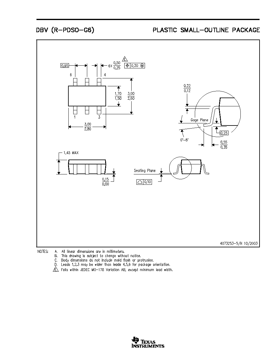
OPA695
31
SBOS293B
www.ti.com
PACKAGE DRAWINGS (Cont.)

IMPORTANT NOTICE
Texas Instruments Incorporated and its subsidiaries (TI) reserve the right to make corrections, modifications,
enhancements, improvements, and other changes to its products and services at any time and to discontinue
any product or service without notice. Customers should obtain the latest relevant information before placing
orders and should verify that such information is current and complete. All products are sold subject to TI's terms
and conditions of sale supplied at the time of order acknowledgment.
TI warrants performance of its hardware products to the specifications applicable at the time of sale in
accordance with TI's standard warranty. Testing and other quality control techniques are used to the extent TI
deems necessary to support this warranty. Except where mandated by government requirements, testing of all
parameters of each product is not necessarily performed.
TI assumes no liability for applications assistance or customer product design. Customers are responsible for
their products and applications using TI components. To minimize the risks associated with customer products
and applications, customers should provide adequate design and operating safeguards.
TI does not warrant or represent that any license, either express or implied, is granted under any TI patent right,
copyright, mask work right, or other TI intellectual property right relating to any combination, machine, or process
in which TI products or services are used. Information published by TI regarding third-party products or services
does not constitute a license from TI to use such products or services or a warranty or endorsement thereof.
Use of such information may require a license from a third party under the patents or other intellectual property
of the third party, or a license from TI under the patents or other intellectual property of TI.
Reproduction of information in TI data books or data sheets is permissible only if reproduction is without
alteration and is accompanied by all associated warranties, conditions, limitations, and notices. Reproduction
of this information with alteration is an unfair and deceptive business practice. TI is not responsible or liable for
such altered documentation.
Resale of TI products or services with statements different from or beyond the parameters stated by TI for that
product or service voids all express and any implied warranties for the associated TI product or service and
is an unfair and deceptive business practice. TI is not responsible or liable for any such statements.
Following are URLs where you can obtain information on other Texas Instruments products and application
solutions:
Products
Applications
Amplifiers
amplifier.ti.com
Audio
www.ti.com/audio
Data Converters
dataconverter.ti.com
Automotive
www.ti.com/automotive
DSP
dsp.ti.com
Broadband
www.ti.com/broadband
Interface
interface.ti.com
Digital Control
www.ti.com/digitalcontrol
Logic
logic.ti.com
Military
www.ti.com/military
Power Mgmt
power.ti.com
Optical Networking
www.ti.com/opticalnetwork
Microcontrollers
microcontroller.ti.com
Security
www.ti.com/security
Telephony
www.ti.com/telephony
Video & Imaging
www.ti.com/video
Wireless
www.ti.com/wireless
Mailing Address:
Texas Instruments
Post Office Box 655303 Dallas, Texas 75265
Copyright
2004, Texas Instruments Incorporated