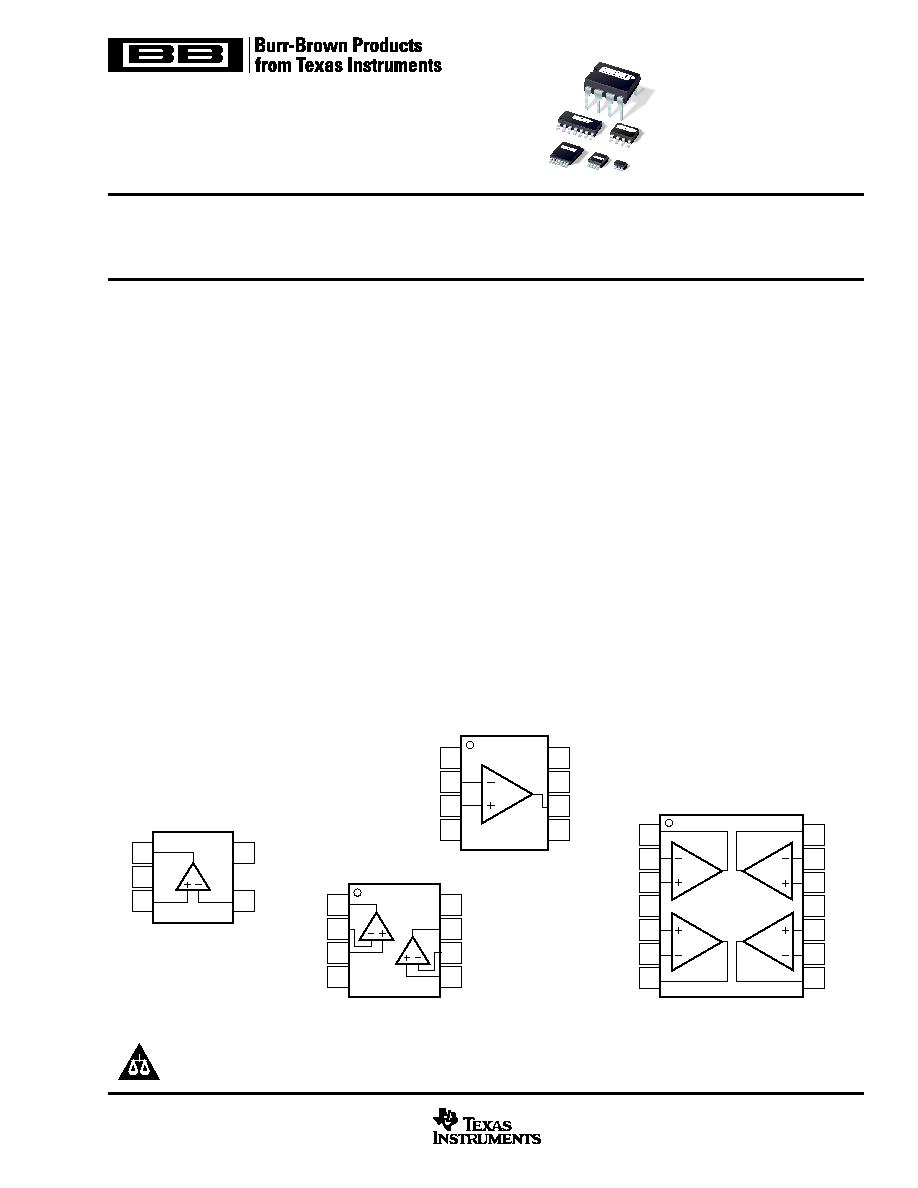
OPA705
OPA2705
OPA4705
Low-Cost, CMOS, Rail-to-Rail, I/O
OPERATIONAL AMPLIFIERS
FEATURES
q
RAIL-TO-RAIL INPUT AND OUTPUT
q
WIDE SUPPLY RANGE:
Single Supply: 4V to 12V
Dual Supplies:
±
2 to
±
6
q
LOW QUIESCENT CURRENT: 160
µ
A
q
LIMITED RANGE CMRR: 96dB
q
LOW OFFSET: 0.5mV
q
HIGH SPEED: 1MHz, 0.6V/
µ
s
q
MicroSIZE PACKAGES:
SOT23-5, MSOP-8, TSSOP-14
q
LOW INPUT BIAS CURRENT: 1pA
APPLICATIONS
q
AUTOMOTIVE APPLICATIONS:
Audio, Sensor Applications, Security Systems
q
PORTABLE EQUIPMENT
q
ACTIVE FILTERS
q
TRANSDUCER AMPLIFIER
q
TEST EQUIPMENT
q
DATA ACQUISITION
DESCRIPTION
The OPA705 series low-cost op amps are optimized for appli-
cations requiring rail-to-rail input and output swing. Single,
dual, and quad versions are offered in a variety of packages.
While the quiescent current is less than 200
µ
A per amplifier,
the OPA705 still offers excellent dynamic performance
(1MHz GBW and 0.6V/
µ
s SR) and unity-gain stability.
The OPA705 series is fully specified and guaranteed over
the supply range of
±
2V to
±
6V. Input swing extends
300mV beyond the rail and the output swings to within
40mV of the rail.
The single version (OPA705) is available in the MicroSIZE
SOT23-5 and in the standard SO-8 surface-mount packages.
The dual version (OPA2705) is available in the MSOP-8,
SO-8, and DIP-8 packages. The quad OPA4705 is available
in the TSSOP-14 and SO-14 packages. All are specified for
operation from ≠40
∞
C to +85
∞
C.
1
2
3
5
4
V+
≠In
Out
V≠
+In
OPA705
SOT23-5
1
2
3
4
8
7
6
5
NC
V+
Out
NC
NC
≠In
+In
V≠
OPA705
SO-8, DIP-8
1
2
3
4
8
7
6
5
V+
Out B
≠In B
+In B
Out A
≠In A
+In A
V≠
OPA2705
MSOP-8, SO-8, DIP-8
A
B
1
2
3
4
5
6
7
14
13
12
11
10
9
8
Out D
≠In D
+In D
V≠
+In C
≠In C
Out C
Out A
≠In A
+In A
V+
+In B
≠In B
Out B
OPA4705
TSSOP-14, SO-14
A
D
B
C
SBOS182A ≠ JUNE 2001
www.ti.com
PRODUCTION DATA information is current as of publication date.
Products conform to specifications per the terms of Texas Instruments
standard warranty. Production processing does not necessarily include
testing of all parameters.
Copyright © 2001, Texas Instruments Incorporated
Please be aware that an important notice concerning availability, standard warranty, and use in critical applications of
Texas Instruments semiconductor products and disclaimers thereto appears at the end of this data sheet.
Æ
OPA705
OPA7
05
OPA7
05
OPA7
05
OPA705, 2705, 4705
2
SBOS182A
MINIMUM
PACKAGE
RECOMMENDED
DRAWING
PACKAGE
ORDERING
TRANSPORT
PRODUCT
DESCRIPTION
GAIN
PACKAGE
NUMBER
MARKING
NUMBER
(1)
MEDIA
OPA705NA
Single, GBW = 1MHz
1
SOT23-5
331
A05
OPA705NA/250
Tape and Reel
"
"
"
"
"
"
OPA705NA/3K
Tape and Reel
OPA705UA
Single, GBW = 1MHz
1
SO-8
182
OPA705UA
OPA705UA
Rails
"
"
"
"
"
"
OPA705UA/2K5
Tape and Reel
OPA705PA
Single, GBW = 1MHz
1
DIP-8
006
OPA705PA
OPA705PA
Rails
OPA2705EA
Dual, GBW = 1MHz
1
MSOP-8
337
B05
OPA2705EA/250
Tape and Reel
"
"
"
"
"
"
OPA2705EA/2K5
Tape and Reel
OPA2705UA
Dual, GBW = 1MHz
1
SO-8
182
OPA2705UA
OPA2705UA
Rails
"
"
"
"
"
"
OPA2705UA/2K5
Tape and Reel
OPA2705PA
Dual, GBW = 1MHz
1
DIP-8
006
OPA2705PA
OPA2705PA
Rails
OPA4705EA
Quad, GBW = 1MHz
1
TSSOP-14
357
OPA4705EA
OPA4705EA/250
Tape and Reel
"
"
"
"
"
"
OPA4705EA/2K5
Tape and Reel
OPA4705UA
Quad, GBW = 1MHz
1
SO-14
235
OPA4705UA
OPA4705UA
Rails
"
"
"
"
"
"
OPA4705UA/2K5
Tape and Reel
NOTE: (1) Models with a slash (/) are available only in Tape and Reel in the quantities indicated (e.g., /3K indicates 3000 devices per reel). Ordering 3000 pieces
of "OPA705NA/3K" will get a single 3000-piece Tape and Reel.
PACKAGE/ORDERING INFORMATION
Supply Voltage, V+ to V≠ ................................................................. 13.2V
Signal Input Terminals, Voltage
(2)
..................... (V≠) ≠0.3V to (V+) +0.3V
Current
(2)
.................................................... 10mA
Output Short-Circuit
(3)
.............................................................. Continuous
Operating Temperature .................................................. ≠55
∞
C to +125
∞
C
Storage Temperature ..................................................... ≠65
∞
C to +150
∞
C
Junction Temperature .................................................................... +150
∞
C
Lead Temperature (soldering, 10s) ............................................... +300
∞
C
NOTES: (1) Stresses above these ratings may cause permanent damage.
Exposure to absolute maximum conditions for extended periods may
degrade device reliability. (2) Input terminals are diode-clamped to the power
supply rails. Input signals that can swing more than 0.3V beyond the supply
rails should be current-limited to 10mA or less. (3) Short-circuit to ground,
one amplifier per package.
ABSOLUTE MAXIMUM RATINGS
(1)
ELECTROSTATIC
DISCHARGE SENSITIVITY
This integrated circuit can be damaged by ESD. Texas Instru-
ments recommends that all integrated circuits be handled with
appropriate precautions. Failure to observe proper handling
and installation procedures can cause damage.
ESD damage can range from subtle performance degrada-
tion to complete device failure. Precision integrated circuits
may be more susceptible to damage because very small
parametric changes could cause the device not to meet its
published specifications.
OPA705, 2705, 4705
3
SBOS182A
OPA705NA, UA, PA
OPA2705EA, UA, PA
OPA4705EA, UA
ELECTRICAL CHARACTERISTICS: V
S
= 4V to 12V
Boldface limits apply over the specified temperature range, T
A
= ≠40
∞
C to +85
∞
C
At T
A
= +25
∞
C, R
L
= 20k
connected to V
S
/ 2 and V
OUT
= V
S
/ 2, unless otherwise noted.
PARAMETER
CONDITION
MIN
TYP
MAX
UNITS
OFFSET VOLTAGE
Input Offset Voltage
V
OS
V
S
=
±
5V, V
CM
= 0V
±
0.5
±
5
mV
Drift
dV
OS
/ dT
T
A
= ≠40
∞
C to +85
∞
C
±
4
µ
V/
∞
C
vs Power Supply
PSRR
V
S
=
±
2V to
±
6V, V
CM
= 0V
20
100
µ
V/V
Over Temperature
V
S
=
±
2V to
±
6V, V
CM
= 0V
100
µ
V/V
Channel Separation, dc
R
L
= 20k
1
µ
V/V
f = 1kHz
98
dB
INPUT VOLTAGE RANGE
Common-Mode Voltage Range
V
CM
(V≠) ≠ 0.3
(V+) + 0.3
V
Common-Mode Rejection Ratio
CMRR
V
S
=
±
5V, (V≠) ≠ 0.3V < V
CM
< (V+) + 0.3V
66
77
dB
over Temperature
V
S
=
±
5V, (V≠) < V
CM
< (V+)
74
dB
V
S
=
±
5V, (V≠) ≠ 0.3V < V
CM
< (V+) ≠ 2V
66
96
dB
over Temperature
V
S
=
±
5V, (V≠) < V
CM
< (V+) ≠ 2V
93
dB
INPUT BIAS CURRENT
Input Bias Current
I
B
V
S
=
±
5V, V
CM
= 0V
±
1
±
10
pA
Input Offset Current
I
OS
V
S
=
±
5V, V
CM
= 0V
±
0.5
±
10
pA
INPUT IMPEDANCE
Differential
4 ∑ 10
9
|| 4
|| pF
Common-Mode
5 ∑ 10
12
|| 4
|| pF
NOISE
Input Voltage Noise, f = 0.1Hz to 10Hz
V
S
=
±
5V, V
CM
= 0V
6
µ
Vp-p
Input Voltage Noise Density, f = 1kHz
e
n
V
S
=
±
5V, V
CM
= 0V
45
nV/
Hz
Current Noise Density, f = 1kHz
i
n
V
S
=
±
5V, V
CM
= 0V
2.5
fA/
Hz
OPEN-LOOP GAIN
Open-Loop Voltage Gain
A
OL
R
L
= 100k
, (V≠)+0.1V < V
O
< (V+)≠0.1V
120
dB
R
L
= 20k
, (V≠)+0.075V < V
O
< (V+)≠0.075V
100
110
dB
over Temperature
R
L
= 20k
, (V≠)+0.075V < V
O
< (V+)≠0.075V
106
dB
R
L
= 5k
, (V≠)+0.15V < V
O
< (V+)≠0.15V
100
110
dB
over Temperature
R
L
= 5k
, (V≠)+0.15V < V
O
< (V+)≠0.15V
106
dB
OUTPUT
Voltage Output Swing from Rail
R
L
= 100k
, A
OL
> 80dB
40
mV
R
L
= 20k
, A
OL
> 100dB
75
mV
R
L
= 5k
, A
OL
> 100dB
150
mV
Output Current
I
OUT
|V
S
≠ V
OUT
| < 1V
±
10
mA
Short-Circuit Current
I
SC
±
40
mA
Capacitive Load Drive
C
LOAD
See Typical Performance Curves
FREQUENCY RESPONSE
C
L
= 100pF
Gain-Bandwidth Product
GBW
G = +1
1
MHz
Slew Rate
SR
V
S
=
±
5V, G = +1
0.6
V/
µ
s
Settling Time, 0.1%
t
S
V
S
=
±
5V, 5V Step, G = +1
15
µ
s
0.01%
V
S
=
±
5V, 5V Step, G = +1
20
µ
s
Overload Recovery Time
V
IN
∑ Gain = V
S
3
µ
s
Total Harmonic Distortion + Noise
THD+N
V
S
=
±
5V, V
O
= 3Vp-p, G = +1, f = 1kHz
0.02
%
POWER SUPPLY
Specified Voltage Range, Single Supply
V
S
4
12
V
Specified Voltage Range, Dual Supplies
V
S
±
2
±
6
V
Operating Voltage Range
3.6 to 12
V
Quiescent Current (per amplifier)
I
Q
I
O
= 0
160
250
µ
A
over Temperature
200
µ
A
TEMPERATURE RANGE
Specified Range
≠40
85
∞
C
Operating Range
≠55
125
∞
C
Storage Range
≠65
150
∞
C
Thermal Resistance
JA
SOT23-5 Surface-Mount
200
∞
C/W
MSOP-8 Surface-Mount
150
∞
C/W
TSSOP-14 Surface-Mount
100
∞
C/W
SO-8 Surface Mount
150
∞
C/W
SO-14 Surface Mount
100
∞
C/W
DIP-8
100
∞
C/W
OPA705, 2705, 4705
4
SBOS182A
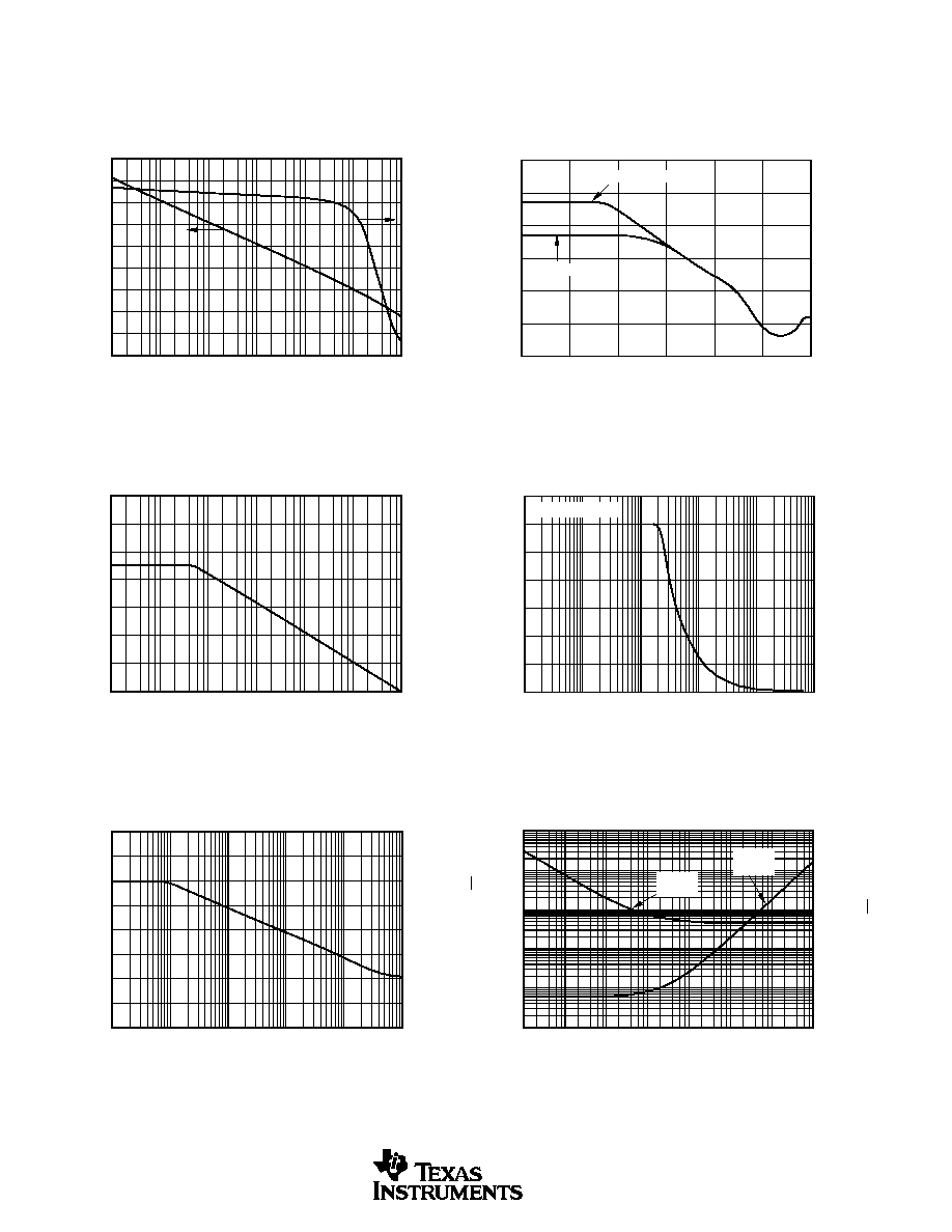
TYPICAL CHARACTERISTICS
At T
A
= +25
∞
C, V
S
=
±
5V, and R
L
= 20k
, unless otherwise noted.
GAIN AND PHASE vs FREQUENCY
10
Gain (dB)
Frequency (Hz)
100
10k
1k
100k
1M
10M
120
100
80
60
40
20
0
≠20
≠40
≠60
120
100
80
60
40
20
0
≠20
≠40
≠60
Phase (
∞
)
CMRR vs FREQUENCY
1
CMRR (dB)
Frequency (Hz)
10
1k
100
10k
100k
1M
120
100
80
60
40
20
0
CMRR Full Scale
CMRR Limited Range
PSRR vs FREQUENCY
1
PSRR (dB)
Frequency (Hz)
10
1k
100
10k
100k
1M
140
120
100
80
60
40
20
0
CHANNEL SEPARATION vs FREQUENCY
10
Channel Separation (dB)
Frequency (Hz)
100
1k
10k
100k
1M
160
140
120
100
80
60
40
20
0
INPUT CURRENT AND VOLTAGE
SPECTRAL NOISE vs FREQUENCY
0.1
Input Current and Voltage
Spectral Noise nV/
Hz
Frequency (Hz)
10
1
100
1k
10k
100k
1M
10000
1000
100
10
1
0.1
Current
Noise
Voltage
Noise
Output Current Spectral
Noise fA/
Hz
10000
1000
100
10
1
0.1
MAXIMUM AMPLITUDE vs FREQUENCY
100
Amplitude (V)
Frequency (Hz)
1k
10k
100k
1M
10M
7
6
5
4
3
2
1
0
(V+) ≠ (V≠) = 12V

OPA705, 2705, 4705
5
SBOS182A
TYPICAL CHARACTERISTICS
(Cont.)
At T
A
= +25
∞
C, V
S
=
±
5V, and R
L
= 20k
, unless otherwise noted.
COMMON-MODE REJECTION RATIO
vs TEMPERATURE
≠80
CMRR (dB)
Temperature (
∞
C)
≠40
≠60
≠20
20
0
40
60
80
100 120 140
120
110
100
90
80
70
60
Limited Scale
Full Scale
OPEN-LOOP GAIN vs TEMPERATURE
≠100
A
OL
(dB)
Temperature (
∞
C)
≠50
≠75
≠25
50
0
25
75
100 125 150 175
140
130
120
110
100
90
QUIESCENT CURRENT vs TEMPERATURE
≠100
I
Q
(
µ
A)
Temperature (
∞
C)
≠75 ≠50 ≠25
50
25
0
75
100 125 150 175
250
200
150
100
50
0
PSRR vs TEMPERATURE
≠75
PSRR (dB)
Temperature (
∞
C)
≠25
≠50
0
50
10
25
75
100 110 130 150
120
110
100
90
80
70
60
INPUT BIAS (I
B
) AND OFFSET (I
OS
)
CURRENT vs TEMPERATURE
≠50
Bias Current (pA)
Temperature (
∞
C)
≠25
0
50
25
75
I
B
I
OS
100
125
175
150
100000
10000
1000
100
10
1
0.1
0.0
TOTAL HARMONIC DISTORTION PLUS NOISE
(Load = 5k
, BW = 8kHz, 1.0Vrms, G = +1)
1
THD (%)
Frequency (Hz)
10
1k
100
10k
100k
1.000
0.100
0.010
0.001

OPA705, 2705, 4705
6
SBOS182A
TYPICAL CHARACTERISTICS
(Cont.)
At T
A
= +25
∞
C, V
S
=
±
5V, and R
L
= 20k
, unless otherwise noted.
INPUT BIAS CURRENT (I
B
)
vs COMMON-MODE VOLTAGE (V
CM
)
TEMPERATURE =
∞
25C
≠6
Input Bias Current (pA)
Common-Mode Voltage, V
CM
(V)
≠5
≠4
≠3
≠1
0
≠2
1
2
3
4
5
6
15
10
5
0
≠5
≠10
≠15
QUIESCENT CURRENT vs SUPPLY VOLTAGE
2
Quiescent Current (
µ
A)
Supply Voltage (V)
4
8
6
10
12
14
200
190
180
170
160
150
140
130
120
SHORT-CIRCUIT CURRENT
vs SUPPLY VOLTAGE
2
Short-Circuit Current (mA)
Supply Voltage (V)
4
8
6
10
12
14
60
50
40
30
20
10
0
I
SC
P (Sourcing)
I
SC
N (Sinking)
OUTPUT VOLTAGE SWING vs OUTPUT CURRENT
0
Output Voltage (V)
Output Current (
±
mA)
10
20
40
30
50
60
70
6
4
2
0
≠2
≠4
≠6
Sourcing
Sinking
+125
∞
C +25
∞
C
≠55
∞
C
+125
∞
C
+25
∞
C
≠55
∞
C
SMALL-SIGNAL OVERSHOOT (%)
vs CAPACITIVE LOAD AND GAIN
10
Overshoot (%)
Load Capacitance Value (pF)
100
1k
10k
90
80
70
60
50
40
30
20
10
0
G = +1
G = ≠1
G
= +5
INPUT BIAS CURRENT (I
B
)
vs COMMON-MODE VOLTAGE (V
CM
)
TEMPERATURE = 125
∞
C
≠6
Input Bias Current (nA)
Common-Mode Voltage, V
CM
(V)
≠5
≠4
≠3
≠1
0
≠2
1
2
3
4
5
6
20
15
10
5
0
≠5
≠10
OPA705, 2705, 4705
7
SBOS182A
TYPICAL CHARACTERISTICS
(Cont.)
At T
A
= +25
∞
C, V
S
=
±
5V, and R
L
= 20k
, unless otherwise noted.
SETTLING TIME vs GAIN
1
Settling Time (
µ
s)
Non-Inverting Gain (V/V)
10
100
100
90
80
70
60
50
40
30
20
10
0.1%
0.01%
V
OS
PRODUCTION DISTRIBUTION
Frequency (%)
Voltage Offset (mV)
≠
5.0
≠
4.5
≠
4.0
≠
3.5
≠
3.0
≠
2.5
≠
2.0
≠
1.5
≠
1.0
≠
0.5
0.1
0.5
1.0
1.5
2.0
2.5
3.0
3.5
4.0
4.5
5.0
25
20
15
10
5
0
V
OS
DRIFT PRODUCTION DISTRIBUTION
Frequency (%)
Voltage Offset (
µ
V/
∞
C)
30
24
18
12
6
< 0
< 6
< 12
< 18
< 24
< 30
27
21
15
9
3
< 3
< 9
< 15
< 21
< 27
> 30
25
20
15
10
5
0
SMALL SIGNAL STEP RESPONSE
(G = +1V/V, R
L
= 20k
, C
L
= 100pF)
5
µ
s/div
50mV/div
LARGE SIGNAL STEP RESPONSE
(G = +1V/V, R
L
= 20k
, C
L
= 100pF)
10
µ
s/div
1V/div

OPA705, 2705, 4705
8
SBOS182A
APPLICATIONS INFORMATION
OPA705 series op amps can operate on 160
µ
A quiescent
current from a single (or split) supply in the range of 4V to
12V (
±
2V to
±
6V), making them highly versatile and easy
to use. The OPA705 is unity-gain stable and offers 1MHz
bandwidth and 0.6V/
µ
s slew rate.
Rail-to-rail input and output swing helps maintain dynamic
range, especially in low supply applications. Figure 1 shows
the input and output waveforms for the OPA705 in unity-
gain configuration. Operation is from a
±
5V supply with a
100k
load connected to V
S
/2. The input is a 10Vp-p
sinusoid. Output voltage is approximately 10Vp-p.
Power-supply pins should be bypassed with 1000pF ceramic
capacitors in parallel with 1
µ
F tantalum capacitors.
OPERATING VOLTAGE
OPA705 series op amps are fully specified and guaranteed
from +4V to +12V over a temperature range of ≠40∫C to
+85∫C. Parameters that vary significantly with operating volt-
ages or temperature are shown in the Typical Characteristics.
RAIL-TO-RAIL INPUT
The input common-mode voltage range of the OPA705 series
extends 300mV beyond the supply rails at room temperature.
This is achieved with a complementary input stage--an N-
channel input differential pair in parallel with a P-channel
differential pair, as shown in Figure 2. The N-channel pair is
active for input voltages close to the positive rail, typically
(V+) ≠ 2.0V to 300mV above the positive supply, while the P-
channel pair is on for inputs from 300mV below the negative
supply to approximately (V+) ≠ 1.5V. There is a small
transition region, typically (V+) ≠ 2.0V to (V+) ≠ 1.5V, in
which both pairs are on. This 500mV transition region can
vary
±
100mV with process variation. Thus, the transition
region (both stages on) can range from (V+) ≠ 2.1V to (V+)
≠ 1.4V on the low end, up to (V+) ≠ 1.9V to (V+) ≠ 1.6V on
the high end. Within the 500mV transition region PSRR,
CMRR, offset voltage, and offset drift, and THD may vary
compared to operation outside this region.
FIGURE 2. Simplified Schematic.
FIGURE 1. Rail-to-Rail Input and Output.
Input
Output (inverted on scope)
2.0V/div
G = +1, V
S
=
±
5V
200
µ
s/div
V
O
V≠
V+
V
IN
+
V
IN
≠

OPA705, 2705, 4705
9
SBOS182A
RAIL-TO-RAIL OUTPUT
A class AB output stage with common-source transistors is
used to achieve rail-to-rail output. This output stage is
capable of driving 1k
loads connected to any point be-
tween V+ and ground. For light resistive loads (> 100k
),
the output voltage can swing to 40mV from the supply rail.
With moderate resistive loads (20k
), the output can swing
to within 75mV from the supply rails while maintaining high
open-loop gain (see the typical performance curve "Output
Voltage Swing vs Output Current").
CAPACITIVE LOAD AND STABILITY
The OPA705 series op amps can drive up to 1000pF pure
capacitive load. Increasing the gain enhances the amplifier's
ability to drive greater capacitive loads (see the typical
performance curve "Small Signal Overshoot vs Capacitive
Load").
One method of improving capacitive load drive in the unity-
gain configuration is to insert a 10
to 20
resistor inside the
feedback loop, as shown in Figure 5. This reduces ringing
with large capacitive loads while maintaining DC accuracy.
FIGURE 5. Series Resistor in Unity-Gain Buffer Configura-
tion Improves Capacitive Load Drive.
INPUT VOLTAGE
Device inputs are protected by ESD diodes that will conduct
if the input voltages exceed the power supplies by more than
approximately 300mV. Momentary voltages greater than
300mV beyond the power supply can be tolerated if the
current is limited to 10mA. This is easily accomplished with
an input resistor, as shown in Figure 3. Many input signals
are inherently current-limited to less than 10mA; therefore,
a limiting resistor is not always required. The OPA705
features no phase inversion when the inputs extend beyond
supplies if the input current is limited, as seen in Figure 4.
FIGURE 4. OPA705--No Phase Inversion with Inputs
Greater than the Power-Supply Voltage.
FIGURE 3. Input Current Protection for Voltages Exceeding
the Supply Voltage.
2.0V/div
V
S
=
±
5.0V, V
IN
= 11Vp-p
20
µ
s/div
APPLICATION CIRCUITS
The OPA705 series op amps are optimized for driving
medium-speed sampling data converters. Figure 6 shows the
OPA2705 in a dual-supply buffered reference configuration
for the DAC7644. The DAC7644 is a 16-bit, low-power,
quad-voltage output converter. Small size makes the combi-
nation ideal for automatic test equipment, data acquisition
systems, and other low-power space-limited applications.
R
OPA705
10mA max
+V
V≠
V
IN
V
OUT
I
OVERLOAD
R
S
20
OPA705
C
L
R
L
V
IN
V
OUT
OPA705, 2705, 4705
10
SBOS182A
FIGURE 6. OPA705 as Dual Supply Configuration-Buffered References for the DAC7644.
NC
NC
NC
NC
V
OUT
A Sense
V
OUT
A
V
REF
L AB Sense
V
REF
L AB
V
REF
H AB
V
REF
H AB Sense
V
OUT
B Sense
V
OUT
B
48
47
46
45
44
43
42
41
40
39
38
37
DAC7644
500pF
+V
1/2
OPA2705
Ref
1/2
OPA2705
500pF
+2.5V
≠V
V+
V
OUT
V
OUT
Ref
≠2.5V
Negative
Reference
Positive
Reference
V≠

PACKAGING INFORMATION
ORDERABLE DEVICE
STATUS(1)
PACKAGE TYPE
PACKAGE DRAWING
PINS
PACKAGE QTY
OPA2705EA/250
ACTIVE
VSSOP
DGK
8
250
OPA2705EA/2K5
ACTIVE
VSSOP
DGK
8
2500
OPA2705PA
ACTIVE
PDIP
P
8
50
OPA2705UA
ACTIVE
SOIC
D
8
100
OPA2705UA/2K5
ACTIVE
SOIC
D
8
2500
OPA4705EA/250
ACTIVE
TSSOP
PW
14
250
OPA4705EA/2K5
ACTIVE
TSSOP
PW
14
2500
OPA4705UA
ACTIVE
SOIC
D
14
58
OPA4705UA/2K5
ACTIVE
SOIC
D
14
2500
OPA705NA/250
ACTIVE
SOP
DBV
5
250
OPA705NA/3K
ACTIVE
SOP
DBV
5
3000
OPA705PA
ACTIVE
PDIP
P
8
50
OPA705UA
ACTIVE
SOIC
D
8
100
OPA705UA/2K5
ACTIVE
SOIC
D
8
2500
(1) The marketing status values are defined as follows:
ACTIVE: Product device recommended for new designs.
LIFEBUY: TI has announced that the device will be discontinued, and a lifetime-buy period is in effect.
NRND: Not recommended for new designs. Device is in production to support existing customers, but TI does not recommend using this part in
a new design.
PREVIEW: Device has been announced but is not in production. Samples may or may not be available.
OBSOLETE: TI has discontinued the production of the device.
PACKAGE OPTION ADDENDUM
www.ti.com
3-Oct-2003

IMPORTANT NOTICE
Texas Instruments Incorporated and its subsidiaries (TI) reserve the right to make corrections, modifications,
enhancements, improvements, and other changes to its products and services at any time and to discontinue
any product or service without notice. Customers should obtain the latest relevant information before placing
orders and should verify that such information is current and complete. All products are sold subject to TI's terms
and conditions of sale supplied at the time of order acknowledgment.
TI warrants performance of its hardware products to the specifications applicable at the time of sale in
accordance with TI's standard warranty. Testing and other quality control techniques are used to the extent TI
deems necessary to support this warranty. Except where mandated by government requirements, testing of all
parameters of each product is not necessarily performed.
TI assumes no liability for applications assistance or customer product design. Customers are responsible for
their products and applications using TI components. To minimize the risks associated with customer products
and applications, customers should provide adequate design and operating safeguards.
TI does not warrant or represent that any license, either express or implied, is granted under any TI patent right,
copyright, mask work right, or other TI intellectual property right relating to any combination, machine, or process
in which TI products or services are used. Information published by TI regarding third-party products or services
does not constitute a license from TI to use such products or services or a warranty or endorsement thereof.
Use of such information may require a license from a third party under the patents or other intellectual property
of the third party, or a license from TI under the patents or other intellectual property of TI.
Reproduction of information in TI data books or data sheets is permissible only if reproduction is without
alteration and is accompanied by all associated warranties, conditions, limitations, and notices. Reproduction
of this information with alteration is an unfair and deceptive business practice. TI is not responsible or liable for
such altered documentation.
Resale of TI products or services with statements different from or beyond the parameters stated by TI for that
product or service voids all express and any implied warranties for the associated TI product or service and
is an unfair and deceptive business practice. TI is not responsible or liable for any such statements.
Following are URLs where you can obtain information on other Texas Instruments products and application
solutions:
Products
Applications
Amplifiers
amplifier.ti.com
Audio
www.ti.com/audio
Data Converters
dataconverter.ti.com
Automotive
www.ti.com/automotive
DSP
dsp.ti.com
Broadband
www.ti.com/broadband
Interface
interface.ti.com
Digital Control
www.ti.com/digitalcontrol
Logic
logic.ti.com
Military
www.ti.com/military
Power Mgmt
power.ti.com
Optical Networking
www.ti.com/opticalnetwork
Microcontrollers
microcontroller.ti.com
Security
www.ti.com/security
Telephony
www.ti.com/telephony
Video & Imaging
www.ti.com/video
Wireless
www.ti.com/wireless
Mailing Address:
Texas Instruments
Post Office Box 655303 Dallas, Texas 75265
Copyright
2003, Texas Instruments Incorporated