FEATURES
D
OFFSET: 15
µ
V (typ), 150
µ
V (max)
D
DRIFT: 0.3
µ
V/
∞
C (typ), 1.5
µ
V/
∞
C (max)
D
BANDWIDTH: 20MHz
D
SLEW RATE: 30V/
µ
s
D
BIAS CURRENT: 100pA (max)
D
LOW NOISE: 6nV/
Hz at 100kHz
D
THD+N: 0.0003% at 1kHz
D
QUIESCENT CURRENT: 4.3mA/ch
D
SUPPLY VOLTAGE: 4V to 12V
D
SHUTDOWN MODE (OPA728): 6
µ
A
APPLICATIONS
D
OPTICAL NETWORKING
D
TRANSIMPEDANCE AMPLIFIERS
D
INTEGRATORS
D
ACTIVE FILTERS
D
A/D CONVERTER DRIVERS
D
I/V CONVERTER FOR DACs
D
HIGH PERFORMANCE AUDIO
D
PROCESS CONTROL
D
TEST EQUIPMENT
OPAx727 AND OPAx728 RELATED PRODUCTS
FEATURES
PRODUCT
20MHz, 3mV, 4
µ
V/
∞
C
(non-etrim version of OPA727)
OPA725
20MHz, 3mV, 4
µ
V/
∞
C, Shutdown
(non-etrim version of OPA728)
OPA726
-
V
B
V
OUT
+12V
OPA727
DESCRIPTION
The OPA727 and OPA728 series op amps use a
state-of-the-art 12V analog CMOS process and e-trim, a
package-level trim, offering outstanding dc precision and
ac performance. The extremely low offset (150
µ
V max)
and drift (1.5
µ
V/
∞
C) are achieved by trimming the IC
digitally after packaging to avoid the shift in parameters as
a result of stresses during package assembly. To correct
for offset drift, the OPA727/OPA728 family is trimmed over
temperature. The devices feature very high CMRR and
open loop gain to minimize errors.
Excellent ac characteristics, such as 20MHz GBW, 30V/
µ
s
slew rate and 0.0003% THD+N make the OPA727 and
OPA728 well-suited for communication, high-end audio,
and active filter applications. With a bias current of less
than 100pA, they are ideal for use as transimpedance
(I/V-conversion) amplifiers for monitoring optical power in
ONET applications.
Optimized for single-supply operation up to 12V, the input
common-mode range extends to GND for true
single-supply functionality. The output swings to within
150mV of the rails, maximizing dynamic range. The low
quiescent current of 4.3mA makes it well-suited for use in
battery-operated equipment. The OPA728 shutdown
version reduces the quiescent current to typically 6
µ
A and
features a reference pin for easy shutdown operation with
standard CMOS logic in dual-supply applications.
For ease of use, the OPA727 and OPA728 op amp families
are fully specified and tested over the supply range of 4V
to 12V. The OPA727 (single) and OPA728 (single with
shutdown) are available in MSOP-8 and DFN-8; the
OPA2727 (dual) is available in DFN-8 and SO-8, and the
quad version OPA4727 will be available Q1'05 in
TSSOP-14. All versions are specified for operation from
-40
∞
C to +125
∞
C.
OPA727, OPA2727
OPA4727, OPA728
SBOS314B - SEPTEMBER 2004 - REVISED DECEMBER 2004
e-trim
20MHz, High Precision CMOS
Operational Amplifier
PRODUCTION DATA information is current as of publication date. Products
conform to specifications per the terms of Texas Instruments standard warranty.
Production processing does not necessarily include testing of all parameters.
www.ti.com
Copyright
2004, Texas Instruments Incorporated
Please be aware that an important notice concerning availability, standard warranty, and use in critical applications of Texas Instruments
semiconductor products and disclaimers thereto appears at the end of this data sheet.
e-trim
is a trademark of Texas Instruments, Incorporated. All other trademarks are the property of their respective owners.

OPA727, OPA2727
OPA4727, OPA728
SBOS314B - SEPTEMBER 2004 - REVISED DECEMBER 2004
www.ti.com
2
PACKAGE/ORDERING INFORMATION
(1)
PRODUCT
PACKAGE-LEAD
PACKAGE DESIGNATOR
PACKAGE MARKING
Non-Shutdown
OPA727
MSOP-8
DGK
AUE
OPA727
DFN-8
DRB
NSF
OPA2727
DFN-8(2)
DRB
NSD
OPA2727
SO-8
D
OPA2727A
OPA4727(2)
TSSOP-14
PW
OPA4727A
Shutdown
OPA728
MSOP-8
DGK
AUF
OPA728
DFN-8
DRB
NSG
(1) For the most current package and ordering information, see the Package Option Addendum located at the end of this datasheet.
(2) Available Q1'05.
ABSOLUTE MAXIMUM RATINGS
(1)
Supply Voltage
+13.2V
. . . . . . . . . . . . . . . . . . . . . . . . . . . . . . . . . . . .
Signal Input Terminals, Voltage(2)
-0.5V to (V+) + 0.5V
. . . . . . . . .
Current(2)
±
10mA
. . . . . . . . . . . . . . . . . . .
Output Short Circuit(3) Continuous
. . . . . . . . . . . . . . . . . . . . . . . . .
Operating Temperature
-55
∞
C to +125
∞
C
. . . . . . . . . . . . . . . . . . . . .
Storage Temperature
-55
∞
C to +150
∞
C
. . . . . . . . . . . . . . . . . . . . . . .
Junction Temperature
+150
∞
C
. . . . . . . . . . . . . . . . . . . . . . . . . . . . . . .
Lead Temperature (soldering, 10s)
+300
∞
C
. . . . . . . . . . . . . . . . . . . .
ESD Rating (Human Body Model)
2000V
. . . . . . . . . . . . . . . . . . . .
(Charged Device Model)
1000V
. . . . . . . . . . . . . . . . .
(1) Stresses above these ratings may cause permanent damage.
Exposure to absolute maximum conditions for extended periods
may degrade device reliability. These are stress ratings only, and
functional operation of the device at these or any other conditions
beyond those specified is not supported.
(2) Input terminals are diode-clamped to the power-supply rails.
Input signals that can swing more than 0.5V beyond the supply
rails should be current limited to 10mA or less.
(3) Short-circuit to ground, one amplifier per package.
This integrated circuit can be damaged by ESD. Texas
Instruments recommends that all integrated circuits be
handled with appropriate precautions. Failure to observe
proper handling and installation procedures can cause damage.
ESD damage can range from subtle performance degradation to
complete device failure. Precision integrated circuits may be more
susceptible to damage because very small parametric changes could
cause the device not to meet its published specifications.
OPA727, OPA2727
OPA4727, OPA728
SBOS314B - SEPTEMBER 2004 - REVISED DECEMBER 2004
www.ti.com
3
PIN CONFIGURATIONS
1
2
3
4
8
7
6
5
V+
OUT B
-
IN B
+IN B
OUT A
-
IN A
+IN A
V
-
OPA2727
SO-8
A
B
1
2
3
4
8
7
6
5
Enable
V+
OUT
NC
(1)
REF
(3)
-
IN
+IN
V
-
OPA728
MSOP-8
1
2
3
4
8
7
6
5
NC
(1)
V+
OUT
NC
(1)
NC
(1)
-
IN
+IN
V
-
OPA727
MSOP-8
1
2
3
4
5
6
7
14
13
12
11
10
9
8
OUT D
-
IN D
+IN D
V+
+IN C
-
IN C
OUT C
OUT A
-
IN A
+IN A
V
-
+IN B
-
IN B
OUT B
OPA4727
(4)
TSSOP-14
A
B
A
B
(1) NC denotes no internal connection.
(2) Connect thermal die pad to V-.
(3) REF is the reference voltage for ENABLE pin.
(4) Available Q1'05.
1
2
3
4
8
7
6
5
NC
(1 )
V+
OUT
NC
(1 )
NC
(1 )
-
IN
+IN
V
-
OPA727
Exposed
Thermal
Die Pad
on
Underside
(2 )
DFN-8
1
2
3
4
8
7
6
5
Enable
V+
OUT
NC
(1)
REF
(3)
-
IN
+IN
V
-
OPA728
Exposed
Thermal
Die Pad
on
Underside
(2)
DFN-8
1
2
3
4
8
7
6
5
V+
OUT B
-
IN B
+IN B
OUT A
-
IN A
+IN A
V
-
OPA2727
(4)
Exposed
Thermal
Die Pad
on
Underside
(2)
DFN-8

OPA727, OPA2727
OPA4727, OPA728
SBOS314B - SEPTEMBER 2004 - REVISED DECEMBER 2004
www.ti.com
4
ELECTRICAL CHARACTERISTICS: V
S
= +4V to +12V or V
S
=
±
2V to
±
6V
Boldface limits apply over the specified temperature range, T
A
= -40
∞
C to +125
∞
C.
At TA = +25
∞
C, RL = 10k
connected to VS/2, and VOUT = VS/2, unless otherwise noted.
OPA727, OPA728, OPA2727
PARAMETER
CONDITIONS
MIN
TYP
MAX
UNIT
OFFSET VOLTAGE
Input Offset Voltage
V
OS
V
S
=
±
5V, V
CM
= 0V
15
150
µ
V
Drift
dV
OS
/dT
0
∞
C to +85
∞
C
0.3
1.5
µ
V/
∞
C
-40
∞
C to +125
∞
C
0.6
3.0
µ
V/
∞
C
vs Power Supply
PSRR
V
S
=
±
2V to
±
6V, V
CM
= V-
30
150
µ
V/V
Over Temperature
V
S
=
±
2V to
±
6V, V
CM
= V-
150
µ
V/V
Channel Separation, dc
1
µ
V/V
INPUT BIAS CURRENT
Input Bias Current, OPA727, OPA728
I
B
±
10
±
100
pA
Input Bias Current, OPA2727
±
60
±
500
pA
Over Temperature
See Typical Characteristics
Input Offset Current
I
OS
±
10
±
100
pA
NOISE
Input Voltage Noise, f = 0.1Hz to 10Hz
e
n
V
S
=
±
6V, V
CM
= 0V
10
µ
V
PP
Input Voltage Noise Density, f = 10kHz
e
n
V
S
=
±
6V, V
CM
= 0V
10
nV/
Hz
Input Voltage Noise Density, f = 100kHz
e
n
V
S
=
±
6V, V
CM
= 0V
6
nV/
Hz
Input Current Noise Density, f = 1kHz
i
n
V
S
=
±
6V, V
CM
= 0V
2.5
fA/
Hz
INPUT VOLTAGE RANGE
Common-Mode Voltage Range
V
CM
(V-)
(V+) - 2.5
V
Common-Mode Rejection Ratio
CMRR
(V-)
V
CM
(V+) - 2.5V
86
94
dB
Over Temperature
(V-)
V
CM
(V+) - 2.5V
84
dB
(V-)
V
CM
(V+) - 3V
94
100
dB
Over Temperature
(V-)
V
CM
(V+) - 3V
84
dB
INPUT IMPEDANCE
Differential
10
11
5
pF
Common-Mode
10
11
4
pF
OPEN-LOOP GAIN
Open-Loop Voltage Gain
A
OL
OPA727, OPA728
R
L
= 100k
, 0.15V < V
O
< (V+) - 0.15V
110
120
dB
Over Temperature
R
L
= 100k
, 0.15V < V
O
< (V+) - 0.15V
100
dB
OPA2727
RL = 100k
, 0.175V < VO < (V+) - 0.175V
110
120
dB
Over Temperature
R
L
= 100k
, 0.175V < V
O
< (V+) - 0.175V
100
dB
OPA727, OPA728
R
L
= 1k
, 0.25V < V
O
< (V+) - 0.25V
106
116
dB
Over Temperature
R
L
= 1k
, 0.25V < V
O
< (V+) - 0.25V
96
dB
OPA2727
R
L
= 2k
, 0.25V < V
O
< (V+) - 0.25V
106
116
dB
Over Temperature
R
L
= 2k
, 0.5V < V
O
< (V+) - 0.5V
96
dB
FREQUENCY RESPONSE
C
L
= 20pF
Gain-Bandwidth Product
GBW
20
MHz
Slew Rate
SR
G = +1
30
V/
µ
s
Settling Time, 0.1%
t
S
V
S
=
±
6V, 5V Step, G = +1
350
ns
0.01%
V
S
=
±
6V, 5V Step, G = +1
450
ns
Overload Recovery Time
V
IN
∑
Gain > V
S
50
ns
Total Harmonic Distortion + Noise
THD+N
VS =
±
6V, VOUT = 2VRMS, RL = 600
,
G = +1, f = 1kHz
0.0003
%

OPA727, OPA2727
OPA4727, OPA728
SBOS314B - SEPTEMBER 2004 - REVISED DECEMBER 2004
www.ti.com
5
ELECTRICAL CHARACTERISTICS: V
S
= +4V to +12V or V
S
=
±
2V to
±
6V (continued)
Boldface limits apply over the specified temperature range, T
A
= -40
∞
C to +125
∞
C.
At TA = +25
∞
C, RL = 10k
connected to VS/2, and VOUT = VS/2, unless otherwise noted.
OPA727, OPA728, OPA2727
PARAMETER
UNIT
MAX
TYP
MIN
CONDITIONS
OUTPUT
Voltage Output Swing from Rail
OPA727, OPA728
R
L
= 100k
, A
OL
> 110dB
100
150
mV
Over Temperature
R
L
= 100k
, A
OL
> 100dB
150
mV
OPA2727
R
L
= 100k
, A
OL
> 110dB
125
175
mV
Over Temperature
R
L
= 100k
, A
OL
> 100dB
175
mV
OPA727, OPA728
R
L
= 1k
, A
OL
> 106dB
200
250
mV
Over Temperature
R
L
= 1k
, A
OL
> 96dB
250
mV
OPA2727
R
L
= 2k
, A
OL
= 106dB
200
250
mV
Over Temperature
R
L
= 2k
, A
OL
= 96dB
500
mV
Output Current
I
OUT
V
S
- V
OUT
< 1V
40
mA
Short-Circuit Current
I
SC
±
55
mA
Capacitive Load Drive
C
LOAD
See Typical Characteristics
Open-Loop Output Impedance
f = 1MHz, I
O
= 0
40
ENABLE/SHUTDOWN (OPA728)
t
OFF
5
µ
s
t
ON
80
µ
s
Enable Reference (Ref Pin) Voltage Range
V-
(V+) - 2
V
V
L
(amplifier is disabled)
< V
DGND
+0.8V
V
V
H
(amplifier is enabled)
> V
DGND
+2V
V
Input Bias Current of Enable Pin
5
pA
I
QSD
Amplifier Disabled
6
15
µ
A
POWER SUPPLY
Specified Voltage Range
V
S
4
12
V
Operating Voltage Range
V
S
3.5 to 13.2
V
Quiescent Current (per amplifier)
I
Q
I
O
= 0
4.3
6.5
mA
Over Temperature
6.5
mA
TEMPERATURE RANGE
Specified Range
-40
+125
∞
C
Operating Range
-55
+125
∞
C
Storage Range
-55
+150
∞
C
Thermal Resistance
q
JA
MSOP-8, SO-8
150
∞
C/W
TSSOP-14
100
∞
C/W
DFN-8
46
∞
C/W

OPA727, OPA2727
OPA4727, OPA728
SBOS314B - SEPTEMBER 2004 - REVISED DECEMBER 2004
www.ti.com
6
TYPICAL CHARACTERISTICS
At TA = +25
∞
C, VS =
±
6V, RL = 10k
connected to VS/2, and VOUT = VS/2, unless otherwise noted.
GAIN AND PHASE vs FREQUENCY
Frequency (Hz)
10
100
1k
10k
100k
1M
10M
100M
180
160
140
120
100
80
60
40
20
0
-
20
180
160
140
120
100
80
60
40
20
0
-
20
Ga
i
n
(
d
B
)
P
has
e
(
_
)
Phase
Gain
POWER-SUPPLY REJECTION RATIO vs FREQUENCY
Frequency (Hz)
100
1k
10k
100k
1M
10M
100M
100
90
80
70
60
50
40
30
20
10
0
PS
R
R
(
d
B
)
CHANNEL SEPARATION vs FREQUENCY
Frequency (Hz)
1k
10k
100k
1M
10M
100M
140
120
100
80
60
40
20
C
h
ann
e
l
S
epa
r
a
ti
on
(
d
B
)
COMMON-MODE REJECTION RATIO vs FREQUENCY
Frequency (Hz)
10
100
1k
10k
100k
1M
10M
120
100
80
60
40
20
0
CM
RR
(
d
B
)
(V
-
)
V
CM
(V+)
-
2V
MAXIMUM OUTPUT VOLTAGE vs FREQUENCY
Frequency (Hz)
10k
100k
1M
10M
7
6
5
4
3
2
1
0
A
m
pl
i
t
ud
e
(
V
)
V
S
=
±
6V
Indicates maximum output
for no visible distortion.
INPUT VOLTAGE NOISE SPECTRAL DENSITY
vs FREQUENCY
Frequency (Hz)
10
100
1k
10k
100k
1M
10M
1000
100
10
1
V
o
l
t
ag
e
N
oi
s
e
(
n
V
/
Hz
)

OPA727, OPA2727
OPA4727, OPA728
SBOS314B - SEPTEMBER 2004 - REVISED DECEMBER 2004
www.ti.com
7
TYPICAL CHARACTERISTICS (continued)
At TA = +25
∞
C, VS =
±
6V, RL = 10k
connected to VS/2, and VOUT = VS/2, unless otherwise noted.
INPUT BIAS CURRENT vs COMMON-MODE VOLTAGE
-
6
-
4
-
2
0
2
4
6
Common-Mode Voltage (V)
100k
10k
1k
100
10
-
10
-
100
-
1k
-
10k
-
100k
Inp
u
t
B
i
a
s
C
ur
r
e
nt
(
p
A
)
I
B
<
±
10pA
+125
_
C
+125
_
C
+85
_
C
+85
_
C
+25
_
C
+25
_
C
OPEN-LOOP GAIN vs TEMPERATURE
140
130
120
110
100
90
80
A
OL
(d
B
)
Temperature (
_
C)
-
50
-
25
0
25
50
75
100
125
150
R
L
= 1k
R
L
= 100k
COMMON-MODE REJECTION RATIO vs TEMPERATURE
110
100
90
80
70
60
CM
RR
(
d
B
)
Temperature (
_
C)
-
50
-
25
0
25
50
75
100
125
150
(V
-
)
V
CM
(V+)
-
2V
OFFSET CURRENT vs TEMPERATURE
10k
1k
100
10
1
0.1
0.01
I
OS
(p
A
)
Temperature (
_
C)
-
50
-
25
0
25
50
75
100
125
150
POWER-SUPPLY REJECTION RATIO vs TEMPERATURE
120
100
80
60
PS
R
R
(
d
B)
Temperature (
_
C)
-
50
-
25
0
25
50
75
100
125
150
QUIESCENT CURRENT vs TEMPERATURE
5
4
3
2
1
0
I
Q
(m
A
)
Temperature (
_
C)
-
50
-
25
0
25
50
75
100
125
150

OPA727, OPA2727
OPA4727, OPA728
SBOS314B - SEPTEMBER 2004 - REVISED DECEMBER 2004
www.ti.com
8
TYPICAL CHARACTERISTICS (continued)
At TA = +25
∞
C, VS =
±
6V, RL = 10k
connected to VS/2, and VOUT = VS/2, unless otherwise noted.
QUIESCENT CURRENT vs SUPPLY VOLTAGE
Supply Voltage (V)
3
4
5
6
7
8
9
10
11
12
13
14
5.0
4.8
4.6
4.4
4.2
4.0
3.8
3.6
3.4
3.2
3.0
I
Q
per
A
m
pl
i
f
i
e
r
(
m
A
)
SHORT-CIRCUIT CURRENT vs SUPPLY VOLTAGE
Supply Voltage (V)
3.
5
4.
5
5.
5
6.
5
7.
5
8.
5
9.
5
10
.5
11
.5
12
.5
13
.5
90
80
70
60
50
40
30
20
10
0
Sh
o
r
t
-
C
i
rc
u
i
t
C
u
r
re
n
t
(m
A
)
Sourcing
Sinking
TOTAL HARMONIC DISTORTION + NOISE vs FREQUENCY
Frequency (Hz)
10
100
1k
10k
100k
0.01
0.001
0.0001
TH
D
+
N
o
i
s
e
(
%)
R
L
= 600
V
OUT
= 2Vrms
BW = 80kHz
SHORT-CIRCUIT CURRENT vs TEMPERATURE
90
80
70
60
50
40
30
20
10
0
S
hor
t-
C
i
r
c
u
i
t
(
mA
)
Temperature (
_
C)
-
50
-
25
0
25
50
75
100
125
150
Sourcing
Sinking
OUTPUT VOLTAGE SWING vs OUTPUT CURRENT
Output Current (mA)
0
10
20
30
40
50
60
70
80
6
4
2
0
-
2
-
4
-
6
O
u
tp
ut
V
o
l
t
ag
e
(
V
)
125
_
C
-
40
_
C
-
40
_
C
25
_
C
SETTLING TIME vs GAIN
Noninverting Gain (V/V)
1
10
100
5000
4500
4000
3500
3000
2500
2000
1500
1000
500
0
0.01%
0.1%
Settling
T
ime (ns)
OPA727, OPA2727
OPA4727, OPA728
SBOS314B - SEPTEMBER 2004 - REVISED DECEMBER 2004
www.ti.com
9
TYPICAL CHARACTERISTICS (continued)
At TA = +25
∞
C, VS =
±
6V, RL = 10k
connected to VS/2, and VOUT = VS/2, unless otherwise noted.
SMALL-SIGNAL OVERSHOOT vs CAPACITIVE LOAD
Capacitive Load (pF)
10
100
1000
90
80
70
60
50
40
30
20
10
0
O
v
er
s
h
oot
(
%
)
G = +1
G =
-
1
C
F
= 3pF
G = +5
C
F
= 1pF
OFFSET VOLTAGE DRIFT PRODUCTION DISTRIBUTION
(0
_
C to +85
_
C)
P
opul
a
t
i
o
n
Offset Voltage Drift (
µ
V/
_
C)
0
0 .1 0.2 0.3 0 .4 0.5 0 .6 0 .7 0 .8 0.9 1.0 1.1 1 .2 1 .3 1.4 1.5
V
S
=
±
5V
OFFSET VOLTAGE vs TEMPERATURE
Of
f
s
e
t
V
o
l
t
a
g
e
(
µ
V)
Temperature (
_
C)
-
50
300
200
100
0
-
100
-
200
-
300
-
25
0
4
4
25
50
75
100
125
V
S
=
±
5V
5 Representative Units Shown
OFFSET VOLTAGE PRODUCTION DISTRIBUTION
Offset Voltage (
µ
V)
-
150
-
140
-
130
-
120
-
110
-
100
-
90
-
80
-
70
-
60
-
50
-
40
-
30
-
20
-
10
0
10
20
30
40
50
60
70
80
90
10
0
11
0
12
0
13
0
14
0
15
0
P
o
pu
l
a
t
i
on
V
S
=
±
5V
OFFSET VOLTAGE DRIFT PRODUCTION DISTRIBUTION
(
-
40
_
C to +125
_
C)
P
o
pul
a
t
i
o
n
Offset Voltage Drift (
µ
V/
_
C)
0
0.2 0.4 0.6 0.8 1.0 1.2 1 .4
1.8
1.6
2.0 2 .2 2.4 2 .6 2.8 3.0
V
S
=
±
5V
SMALL-SIGNAL STEP RESPONSE
100ns/div
10
mV
/
d
i
v
G = +1
R
L
= 10k
C
L
= 20pF
OPA727, OPA2727
OPA4727, OPA728
SBOS314B - SEPTEMBER 2004 - REVISED DECEMBER 2004
www.ti.com
10
TYPICAL CHARACTERISTICS (continued)
At TA = +25
∞
C, VS =
±
6V, RL = 10k
connected to VS/2, and VOUT = VS/2, unless otherwise noted.
LARGE-SIGNAL STEP RESPONSE
400ns/div
1V
/d
i
v
G = +1
R
L
= 10k
C
L
= 20pF
SMALL-SIGNAL STEP RESPONSE
200ns/div
10
mV
/
d
i
v
C
F
= 2pF
C
F
= 3pF
C
F
= 4pF
10k
C
F
C
L
20pF
G =
-
1
R
F
10k
O P A 7 27
LARGE-SIGNAL STEP RESPONSE
1V
/d
i
v
400ns/div
10k
R
F
10
C
F
4pF
C
L
20pF
G =
-
1
OPA727
k

OPA727, OPA2727
OPA4727, OPA728
SBOS314B - SEPTEMBER 2004 - REVISED DECEMBER 2004
www.ti.com
11
APPLICATIONS INFORMATION
The OPA727 and OPA728 family of op amps use e-trim
,
an adjustment to offset voltage and temperature drift made
during the final steps of manufacturing after the plastic
molding is completed. This compensates for performance
shifts that can occur during the molding process. Through
e-trim, the OPA727 and OPA728 deliver excellent offset
voltage (150
µ
V max) and extremely low offset voltage drift
(1.5
µ
V/
∞
C). Additionally, these 20MHz CMOS op amps
have a fast slew rate, low noise, and excellent PSRR,
CMRR, and A
OL
. They can operate on typically 4.3mA
quiescent current from a single (or split) supply in the range
of 4V to 12V (
±
2V to
±
6V), making them highly versatile
and easy to use. They are stable in a unity-gain
configuration.
Power-supply pins should be bypassed with 1nF ceramic
capacitors in parallel with 1
µ
F tantalum capacitors.
OPERATING VOLTAGE
OPA727 series op amps are specified from 4V to 12V
supplies over a temperature range of -40
∞
C to +125
∞
C.
They will operate well in
±
5V or +5V to +12V power-supply
systems. Parameters that vary significantly with operating
voltage or temperature are shown in the Typical
Characteristics.
ENABLE/SHUTDOWN
OPA727 series op amps require approximately 4.3mA
quiescent current. The enable/shutdown feature of the
OPA728 allows the op amp to be shut off to reduce this
current to approximately 6
µ
A.
The enable/shutdown input is referenced to the Enable
Reference Pin, DGND (see Pin Configurations). This pin
can be connected to logic ground in dual-supply op amp
configurations to avoid level-shifting the enable logic
signal, as shown in Figure 1.
The Enable Reference Pin voltage, V
DGND
, must not
exceed (V+) - 2V. It may be set as low as V-. The amplifier
is enabled when the Enable Pin voltage is greater than
V
DGND
+ 2V. The amplifier is disabled (shutdown) if the
Enable Pin voltage is less than V
DGND
+ 0.8V. The Enable
Pin is connected to internal pull-up circuitry and will enable
the device if left unconnected.
COMMON-MODE VOLTAGE RANGE
The input common-mode voltage range of the OPA727
and OPA728 series extends from V- to (V+) - 2.5V.
Common-mode rejection is excellent throughout the input
voltage range from V- to (V+) - 3V. CMRR decreases
somewhat as the common-mode voltage extends to
(V+) - 2.5V, but remains very good and is tested
throughout this range. See the Electrical Characteristics
table for details.
DGND
Digital
Logic
Enable
OPA728
+12V
a) Single-Supply Configuration
b) Dual-Supply Configuration
DGND
Ref
Ref
Digital
Logic
Enable
OPA728
+5V
-
5V
V
O
V
O
Figure 1. Enable Reference Pin Connection for
Single- and Dual-Supply Configurations
INPUT OVER-VOLTAGE PROTECTION
Device inputs are protected by ESD diodes that will
conduct if the input voltages exceed the power supplies by
more than approximately 300mV. Momentary voltages
greater than 300mV beyond the power supply can be
tolerated if the current is limited to 10mA. This is easily
accomplished with an input resistor in series with the op
amp, as shown in Figure 2. The OPA727 series features
no phase inversion when the inputs extend beyond
supplies, if the input is current limited.
R
OPA727
V+
V
-
V
IN
V
OUT
10mA max
I
OVERLOAD
Figure 2. Input Current Protection for Voltages
Exceeding the Supply Voltage
OPA727, OPA2727
OPA4727, OPA728
SBOS314B - SEPTEMBER 2004 - REVISED DECEMBER 2004
www.ti.com
12
RAIL-TO-RAIL OUTPUT
A class AB output stage with common-source transistors
is used to achieve rail-to-rail output. This output stage is
capable of driving heavy loads connected to any point
between V+ and V-. For light resistive loads ( > 100k
),
the output voltage can swing to 150mV from the supply rail,
while still maintaining excellent linearity (A
OL
> 110dB).
With 1k
resistive loads, the output is specified to swing
to within 250mV from the supply rails with excellent
linearity (see the Typical Characteristics curve, Output
Voltage Swing vs Output Current).
CAPACITIVE LOAD AND STABILITY
Capacitive load drive is dependent upon gain and the
overshoot requirements of the application. Increasing the
gain enhances the ability of the amplifier to drive greater
capacitive loads (see the Typical Characteristics curve,
Small-Signal Overshoot vs Capacitive Load).
One method of improving capacitive load drive in the
unity-gain configuration is to insert a 10
to 20
resistor
inside the feedback loop, as shown in Figure 3. This
reduces ringing with large capacitive loads while
maintaining DC accuracy.
R
S
20
OPA727
C
L
R
L
V
IN
V
OUT
V+
Figure 3. Series Resistor in Unity-Gain Buffer
Configuration Improves Capacitive Load Drive
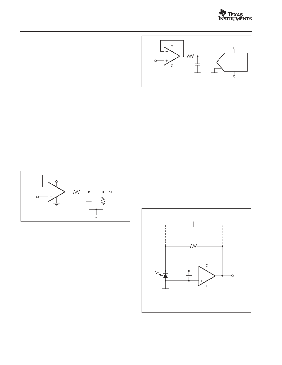
DRIVING FAST 16-BIT ADCs
The OPA727 series is optimized for driving fast 16-bit
ADCs such as the ADS8342. The OPA727 op amps buffer
the converter input capacitance and resulting charge
injection, while providing signal gain. Figure 4 shows the
OPA727 in a single-ended method of interfacing to the
ADS8342 16-bit, 250kSPS, 4-channel ADC with an input
range of
±
2.5V. The OPA727 has demonstrated excellent
settling time to the 16-bit level within the 600ns acquisition
time of the ADS8342. The RC filter, shown in Figure 4, has
been carefully tuned for best noise and settling
performance. It may need to be adjusted for different op
amp configurations. Please refer to the ADS8342 data
sheet (available for download at www.ti.com) for additional
information on this product.
75
OPA727
ADS8342
16-Bit ADC
AIN
Common
330pF
V
IN
±
2.5V
+5V
-
5V
+5V
-
5V
Figure 4. OPA727 Driving an ADC
TRANSIMPEDANCE AMPLIFIER
Wide bandwidth, low input bias current, and low input
voltage and current noise make the OPA727 an ideal
wideband photodiode transimpedance amplifier. Low-
voltage noise is important because photodiode capaci-
tance causes the effective noise gain of the circuit to
increase at high frequency.
The key elements to a transimpedance design, as shown
in Figure 5, are the expected diode capacitance (C
D
),
which should include the parasitic input common-mode
and differential-mode input capacitance (4pF + 5pF for the
OPA727); the desired transimpedance gain (R
F
); and the
GBW for the OPA727 (20MHz). With these three variables
set, the feedback capacitor value (C
F
) can be set to control
the frequency response. C
F
includes the stray capacitance
of R
F
, which is 0.2pF for a typical surface-mount resistor.
OPA727
V
OUT
10M
+5V
-
5V
C
D
R
F
C
F
(1)
< 1pF
NOTE: (1) C
F
is optional to prevent gain peaking.
It includes the stray capacitance of R
F
.
Figure 5. Dual-Supply Transimpedance Amplifier

OPA727, OPA2727
OPA4727, OPA728
SBOS314B - SEPTEMBER 2004 - REVISED DECEMBER 2004
www.ti.com
13
To achieve a maximally-flat, 2nd-order Butterworth
frequency response, the feedback pole should be set to:
1
2
p
R
F
C
F
+
GBW
4
p
R
F
C
D
Bandwidth is calculated by:
f
*
3dB
+
GBW
2
p
R
F
C
D
Hz
For even higher transimpedance bandwidth, the
high-speed CMOS OPA380 (90MHz GBW), OPA354
(100MHz GBW), OPA300 (180 MHz GBW), OPA355
(200MHz GBW), or OPA656, OPA657 (400MHz GBW)
may be used.
For single-supply applications, the +IN input can be biased
with a positive dc voltage to allow the output to reach true
zero when the photodiode is not exposed to any light, and
respond without the added delay that results from coming
out of the negative rail. (Refer to Figure 6.) This bias
voltage also appears across the photodiode, providing a
reverse bias for faster operation.
OPA727
V
OUT
10M
V+
R
F
C
F
(1)
< 1pF
NOTE: (1) C
F
is optional to prevent gain peaking.
It includes the stray capacitance of R
F
.
+V
Bias
Figure 6. Single-Supply Transimpedance
Amplifier
For additional information, refer to Application Bulletin
SBOA055, Compensate Transimpedance Amplifiers
Intuitively, available for download at www.ti.com.
OPTIMIZING THE TRANSIMPEDANCE
CIRCUIT
To achieve the best performance, components should be
selected according to the following guidelines:
1.
For lowest noise, select R
F
to create the total required
gain. Using a lower value for R
F
and adding gain after
the transimpedance amplifier generally produces
poorer noise performance. The noise produced by R
F
increases with the square-root of R
F
, whereas the
signal increases linearly. Therefore, signal-to-noise
ratio is improved when all the required gain is placed
in the transimpedance stage.
2.
Minimize photodiode capacitance and stray
capacitance at the summing junction (inverting input).
This capacitance causes the voltage noise of the op
amp to be amplified (increasing amplification at high
frequency). Using a low-noise voltage source to
reverse-bias a photodiode can significantly reduce its
capacitance. Smaller photodiodes have lower
capacitance. Use optics to concentrate light on a small
photodiode.
3.
Noise increases with increased bandwidth. Limit the
circuit bandwidth to only that required. Use a capacitor
across the R
F
to limit bandwidth, even if not required
for stability.
4.
Circuit board leakage can degrade the performance of
an otherwise well-designed amplifier. Clean the circuit
board carefully. A circuit board guard trace that
encircles the summing junction and is driven at the
same voltage can help control leakage.
For additional information, refer to the Application Bulletins
Noise Analysis of FET Transimpedance Amplifiers
(SBOA060), and Noise Analysis for High-Speed Op Amps
(SBOA066), available for download at the TI web site.
(1)
(2)
OPA727, OPA2727
OPA4727, OPA728
SBOS314B - SEPTEMBER 2004 - REVISED DECEMBER 2004
www.ti.com
14
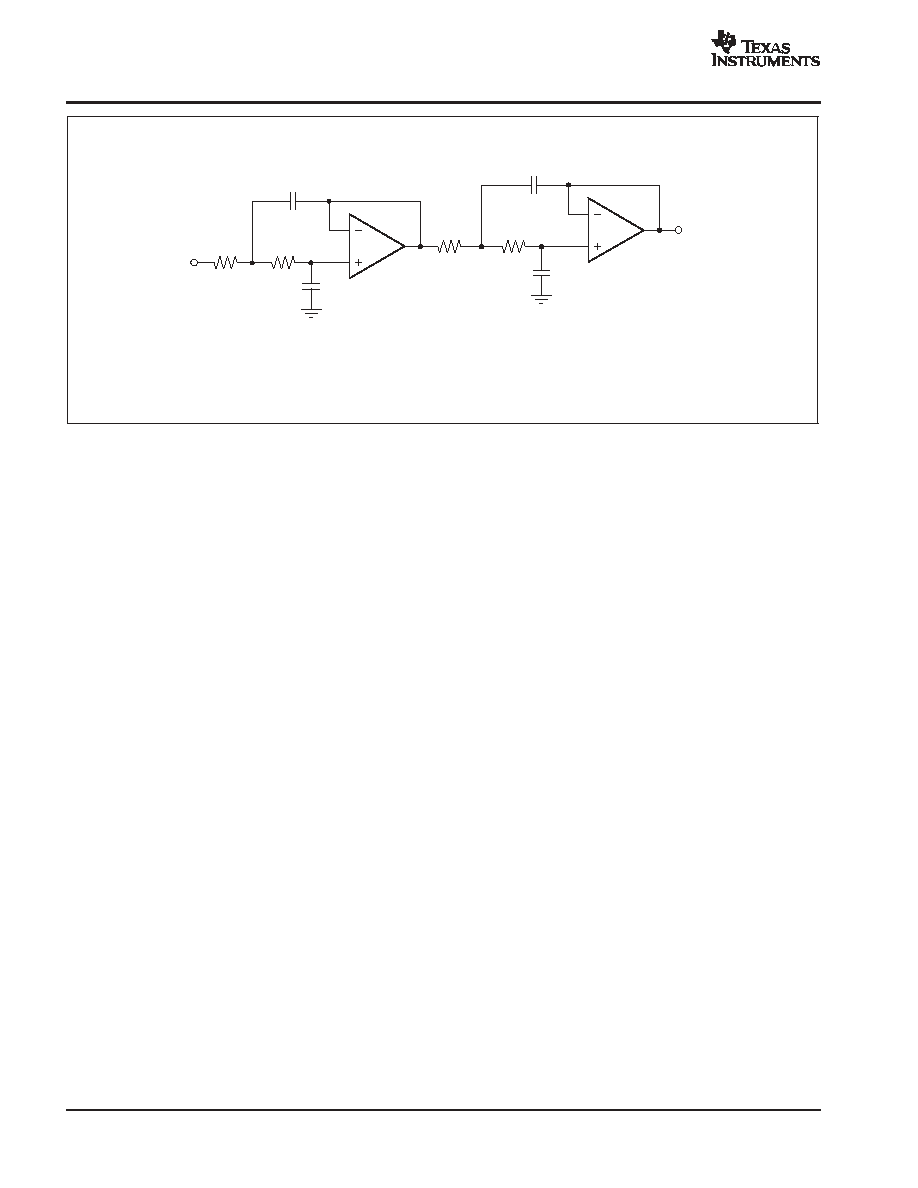
NOTE: FilterPro is a low-pass filter design program available for download at no cost from TI's web site (www.ti.com). The program can be used
to determine component values for other cutoff frequencies or filter types.
DC Gain = 1
1/2
OPA2727
C
1
1nF
C
2
330pF
R
2
15.9k
R
1
1.93k
2.2nF
C
3
C
4
100pF
R
4
22.3k
R
3
2.07k
Cutoff Frequency = 50kHz
1/2
OPA2727
V
O
Figure 7. Four-Pole Butterworth Sallen-Key Low-Pass Filter
DFN PACKAGE
The OPA727 series uses the 8-lead DFN (also known as
SON), which is a QFN package with lead contacts on only
two sides of the bottom of the package. This leadless,
near-chip-scale package maximizes board space and
enhances thermal and electrical characteristics through
an exposed pad.
DFN packages are physically small, have a smaller routing
area, improved thermal performance, and improved
electrical parasitics, with a pinout scheme that is
consistent with other commonly-used packages, such as
SO and MSOP. Additionally, the absence of external leads
eliminates bent-lead issues.
The DFN package can be easily mounted using standard
printed circuit board (PCB) assembly techniques. See
Application Note, QFN/SON PCB Attachment (SLUA271)
and Application Report, Quad Flatpack No-Lead Logic
Packages (SCBA017), both available for download at
www.ti.com.
The exposed leadframe die pad on the bottom of the
package should be connected to V-.
LAYOUT GUIDELINES
The leadframe die pad should be soldered to a thermal pad
on the PCB. A mechanical data sheet showing an example
layout is attached at the end of this data sheet.
Refinements to this layout may be required based on
assembly process requirements. Mechanical drawings
located at the end of this data sheet list the physical
dimensions for the package and pad. The five holes in the
landing pattern are optional, and are intended for use with
thermal vias that connect the leadframe die pad to the
heatsink area on the PCB.
Soldering the exposed pad significantly improves
board-level reliability during temperature cycling, key
push, package shear, and similar board-level tests. Even
with applications that have low-power dissipation, the
exposed pad must be soldered to the PCB to provide
structural integrity and long-term reliability.


PACKAGING INFORMATION
Orderable Device
Status
(1)
Package
Type
Package
Drawing
Pins Package
Qty
Eco Plan
(2)
Lead/Ball Finish
MSL Peak Temp
(3)
OPA727AIDGKR
ACTIVE
MSOP
DGK
8
2500
None
CU NIPDAU
Level-3-240C-168 HR
OPA727AIDGKT
ACTIVE
MSOP
DGK
8
250
None
CU NIPDAU
Level-3-240C-168 HR
OPA727AIDRBR
ACTIVE
SON
DRB
8
3000
None
Call TI
Level-3-260C-168 HR
OPA727AIDRBT
ACTIVE
SON
DRB
8
250
None
Call TI
Level-3-260C-168 HR
OPA728AIDGKR
ACTIVE
MSOP
DGK
8
2500
None
CU NIPDAU
Level-3-240C-168 HR
OPA728AIDGKT
ACTIVE
MSOP
DGK
8
250
None
CU NIPDAU
Level-3-240C-168 HR
OPA728AIDRBR
ACTIVE
SON
DRB
8
3000
None
Call TI
Level-3-260C-168 HR
OPA728AIDRBT
ACTIVE
SON
DRB
8
250
None
Call TI
Level-3-260C-168 HR
(1)
The marketing status values are defined as follows:
ACTIVE: Product device recommended for new designs.
LIFEBUY: TI has announced that the device will be discontinued, and a lifetime-buy period is in effect.
NRND: Not recommended for new designs. Device is in production to support existing customers, but TI does not recommend using this part in
a new design.
PREVIEW: Device has been announced but is not in production. Samples may or may not be available.
OBSOLETE: TI has discontinued the production of the device.
(2)
Eco Plan - May not be currently available - please check
http://www.ti.com/productcontent
for the latest availability information and additional
product content details.
None: Not yet available Lead (Pb-Free).
Pb-Free (RoHS): TI's terms "Lead-Free" or "Pb-Free" mean semiconductor products that are compatible with the current RoHS requirements
for all 6 substances, including the requirement that lead not exceed 0.1% by weight in homogeneous materials. Where designed to be soldered
at high temperatures, TI Pb-Free products are suitable for use in specified lead-free processes.
Green (RoHS & no Sb/Br): TI defines "Green" to mean "Pb-Free" and in addition, uses package materials that do not contain halogens,
including bromine (Br) or antimony (Sb) above 0.1% of total product weight.
(3)
MSL, Peak Temp. -- The Moisture Sensitivity Level rating according to the JEDECindustry standard classifications, and peak solder
temperature.
Important Information and Disclaimer:The information provided on this page represents TI's knowledge and belief as of the date that it is
provided. TI bases its knowledge and belief on information provided by third parties, and makes no representation or warranty as to the
accuracy of such information. Efforts are underway to better integrate information from third parties. TI has taken and continues to take
reasonable steps to provide representative and accurate information but may not have conducted destructive testing or chemical analysis on
incoming materials and chemicals. TI and TI suppliers consider certain information to be proprietary, and thus CAS numbers and other limited
information may not be available for release.
In no event shall TI's liability arising out of such information exceed the total purchase price of the TI part(s) at issue in this document sold by TI
to Customer on an annual basis.
PACKAGE OPTION ADDENDUM
www.ti.com
18-Jan-2005
Addendum-Page 1


IMPORTANT NOTICE
Texas Instruments Incorporated and its subsidiaries (TI) reserve the right to make corrections, modifications,
enhancements, improvements, and other changes to its products and services at any time and to discontinue
any product or service without notice. Customers should obtain the latest relevant information before placing
orders and should verify that such information is current and complete. All products are sold subject to TI's terms
and conditions of sale supplied at the time of order acknowledgment.
TI warrants performance of its hardware products to the specifications applicable at the time of sale in
accordance with TI's standard warranty. Testing and other quality control techniques are used to the extent TI
deems necessary to support this warranty. Except where mandated by government requirements, testing of all
parameters of each product is not necessarily performed.
TI assumes no liability for applications assistance or customer product design. Customers are responsible for
their products and applications using TI components. To minimize the risks associated with customer products
and applications, customers should provide adequate design and operating safeguards.
TI does not warrant or represent that any license, either express or implied, is granted under any TI patent right,
copyright, mask work right, or other TI intellectual property right relating to any combination, machine, or process
in which TI products or services are used. Information published by TI regarding third-party products or services
does not constitute a license from TI to use such products or services or a warranty or endorsement thereof.
Use of such information may require a license from a third party under the patents or other intellectual property
of the third party, or a license from TI under the patents or other intellectual property of TI.
Reproduction of information in TI data books or data sheets is permissible only if reproduction is without
alteration and is accompanied by all associated warranties, conditions, limitations, and notices. Reproduction
of this information with alteration is an unfair and deceptive business practice. TI is not responsible or liable for
such altered documentation.
Resale of TI products or services with statements different from or beyond the parameters stated by TI for that
product or service voids all express and any implied warranties for the associated TI product or service and
is an unfair and deceptive business practice. TI is not responsible or liable for any such statements.
Following are URLs where you can obtain information on other Texas Instruments products and application
solutions:
Products
Applications
Amplifiers
amplifier.ti.com
Audio
www.ti.com/audio
Data Converters
dataconverter.ti.com
Automotive
www.ti.com/automotive
DSP
dsp.ti.com
Broadband
www.ti.com/broadband
Interface
interface.ti.com
Digital Control
www.ti.com/digitalcontrol
Logic
logic.ti.com
Military
www.ti.com/military
Power Mgmt
power.ti.com
Optical Networking
www.ti.com/opticalnetwork
Microcontrollers
microcontroller.ti.com
Security
www.ti.com/security
Telephony
www.ti.com/telephony
Video & Imaging
www.ti.com/video
Wireless
www.ti.com/wireless
Mailing Address:
Texas Instruments
Post Office Box 655303 Dallas, Texas 75265
Copyright
2005, Texas Instruments Incorporated