Burr Brown Products
from Texas Instruments
FEATURES
DESCRIPTION
APPLICATIONS
0
-
10
-
20
-
30
-
40
-
50
-
60
-
70
-
80
Frequency (Hz)
G
a
i
n
(
d
B
)
1k
10k
100k
1M
10M
100M
1G
C
1
C
2
V
IN
R
R
V
OUT
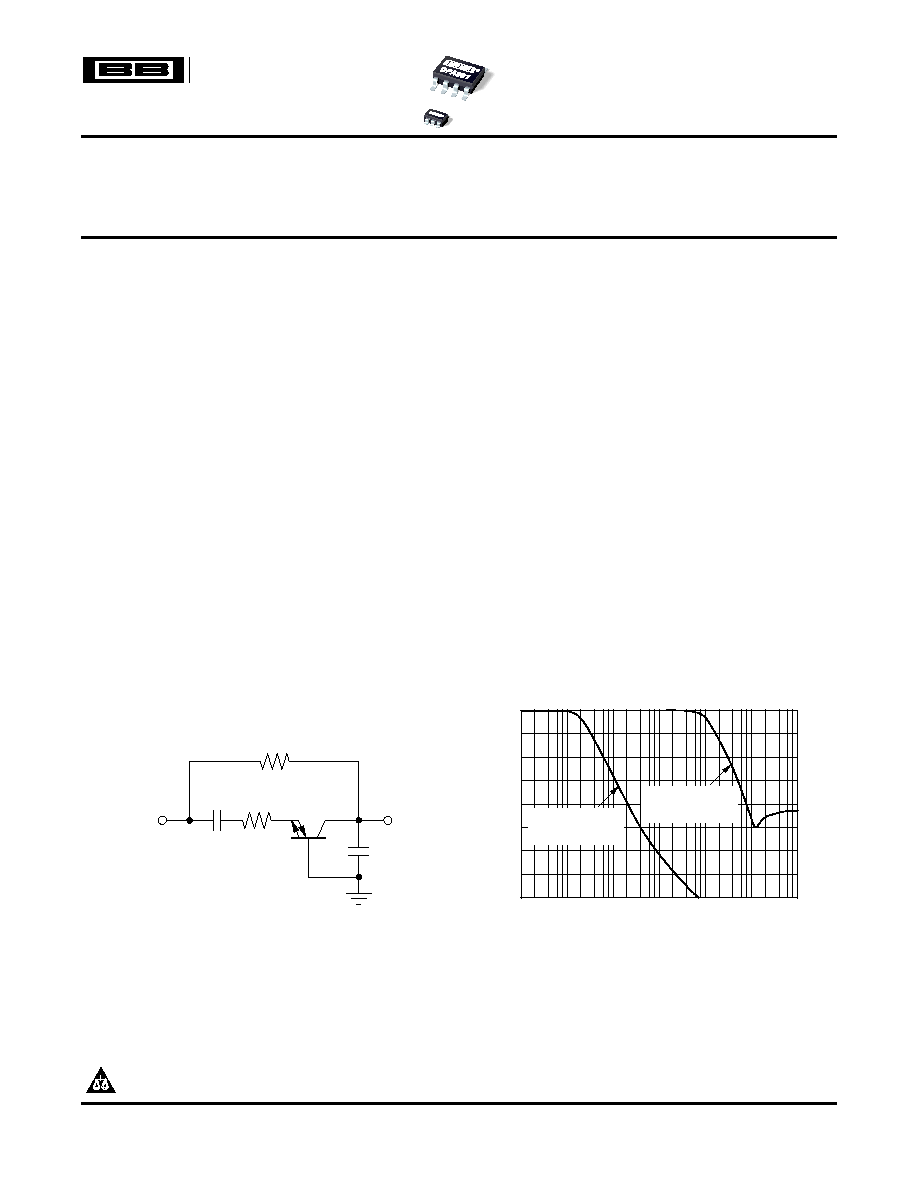
Low-Pass Negative Impedance Converter (NIC) Filter
Frequency Response of 20kHz and 10MHz
Low-Pass NIC Filters
20kHz
Low-Pass Filter
10MHz
Low-Pass Filter
OPA861
SBOS338 ≠ AUGUST 2005
Wide Bandwidth
OPERATIONAL TRANSCONDUCTANCE
AMPLIFIER (OTA)
∑
Wide Bandwidth (80MHz, Open-Loop, G = +5)
The OPA861 is a versatile monolithic component
designed for wide-bandwidth systems, including high
∑
High Slew Rate (900V/µs)
performance video, RF and IF circuitry. The OPA861
∑
High Transconductance (95mA/V)
is a wideband, bipolar operational transconductance
∑
External I
Q
-Control
amplifier (OTA).
∑
Low Quiescent Current (5.4mA)
The OTA or voltage-controlled current source can be
viewed as an ideal transistor. Like a transistor, it has
three terminals--a high impedance input (base), a
∑
Video/Broadcast Equipment
low-impedance input/output (emitter), and the current
output
(collector).
The
OPA861,
however,
is
∑
Communications Equipment
self-biased and bipolar. The output collector current is
∑
High-Speed Data Acquisition
zero for a zero base-emitter voltage. AC inputs
∑
Wideband LED Drivers
centered about zero produce an output current, which
∑
Control Loop Amplifiers
is
bipolar
and
centered
about
zero.
The
∑
Wideband Active Filters
transconductance of the OPA861 can be adjusted
with an external resistor, allowing bandwidth, quiesc-
∑
Line Drivers
ent current, and gain trade-offs to be optimized.
Used as a basic building block, the OPA861 sim-
plifies the design of AGC amplifiers, LED driver
circuits for fiber optic transmission, integrators for fast
pulses, fast control loop amplifiers and control ampli-
fiers for capacitive sensors and active filters. The
OPA861 is available in SO-8 and SOT23-6 sur-
face-mount packages.
Please be aware that an important notice concerning availability, standard warranty, and use in critical applications of Texas
Instruments semiconductor products and disclaimers thereto appears at the end of this data sheet.
PRODUCTION DATA information is current as of publication date.
Copyright © 2005, Texas Instruments Incorporated
Products conform to specifications per the terms of the Texas
Instruments standard warranty. Production processing does not
necessarily include testing of all parameters.
www.ti.com
ABSOLUTE MAXIMUM RATINGS
(1)
1
2
3
4
8
7
6
5
I
Q
Adjust
E
B
V
-
=
-
5V
C
V+ = +5V
NC
NC
SO-8
Top View
1
2
3
6
5
4
I
Q
Adjust
-
V
S
B
+V
S
C
E
SOT23-6
OPA861
SBOS338 ≠ AUGUST 2005
This integrated circuit can be damaged by ESD. Texas Instruments recommends that all integrated
circuits be handled with appropriate precautions. Failure to observe proper handling and installation
procedures can cause damage.
ESD damage can range from subtle performance degradation to complete device failure. Precision
integrated circuits may be more susceptible to damage because very small parametric changes could
cause the device not to meet its published specifications.
ORDERING INFORMATION
(1)
SPECIFIED
PACKAGE
TEMPERATURE
PACKAGE
ORDERING
TRANSPORT MEDIA,
PRODUCT
PACKAGE
DESIGNATOR
RANGE
MARKING
NUMBER
QUANTITY
OPA861ID
Rails, 75
OPA861
SO-8
D
≠45
∞
C to +85
∞
C
OPA861
OPA861IDR
Tape and Reel, 2500
OPA861IDBVT
Tape and Reel, 250
OPA861
SOT23-6
DBV
≠45
∞
C to +85
∞
C
N5R
OPA861IDBVR
Tape and Reel, 3000
(1)
For the most current package and ordering information, see the Package Option Addendum at the end of this document, or see the TI
web site at
www.ti.com
.
Power Supply
±
6.5V
DC
Internal Power Dissipation
See Thermal Information
Differential Input Voltage
±
1.2V
Input Common-Mode Voltage Range
±
V
S
Storage Temperature Range: D
≠40
∞
C to +125
∞
C
Lead Temperature (soldering, 10s)
+260
∞
C
Junction Temperature (T
J
)
+150∞C
ESD Rating:
Human Body Model (HBM)
(2)
1500V
Charge Device Model (CDM)
1000V
(1)
Stresses above these ratings may cause permanent damage. Exposure to absolute maximum conditions for extended periods may
degrade device reliability. These are stress ratings only, and functional operations of the device at these and any other conditions
beyond those specified is not supported.
(2)
Pin 2 for the SO-8 package > 500V HBM. Pin 4 for the SOT23-6 package > 500V HBM.
PIN CONFIGURATION
2

www.ti.com
ELECTRICAL CHARACTERISTICS: V
S
=
±
5V
OPA861
SBOS338 ≠ AUGUST 2005
R
L
= 500
and R
ADJ
= 250
, unless otherwise noted.
OPA861ID, IDBV
TYP
MIN/MAX OVER TEMPERATURE
0
∞
C to
≠40
∞
C to
MIN/
TEST
PARAMETER
CONDITIONS
+25
∞
C
+25
∞
C
(2)
70∞C
(3)
+85∞C
(3)
UNITS
MAX
LEVEL
(1)
OTA -- Open-Loop (see
Figure 30
)
AC PERFORMANCE
G = +5, V
O
= 200mV
PP
,
Bandwidth
80
77
75
74
MHz
min
B
R
L
= 500
G = +5, V
O
= 1V
PP
80
MHz
typ
C
G = +5, V
O
= 5V
PP
80
MHz
typ
C
Slew Rate
G = +5, V
O
= 5V Step
900
860
850
840
V/µs
min
B
Rise Time and Fall Time
V
O
= 1V Step
4.4
ns
typ
C
Harmonic Distortion
G = +5, V
O
= 2V
PP
, 5MHz
2nd-Harmonic
R
L
= 500
≠68
≠55
≠54
≠53
dB
max
B
3rd-Harmonic
R
L
= 500
≠57
≠52
≠51
≠49
dB
max
B
Base Input Voltage Noise
f > 100kHz
2.4
3.0
3.3
3.4
nV/
Hz
max
B
Base Input Current Noise
f > 100kHz
1.7
2.4
2.45
2.5
pA/
Hz
max
B
Emitter Input Current Noise
f > 100kHz
5.2
15.3
16.6
17.5
pA/
Hz
max
B
OTA DC PERFORMANCE
(4)
(see
Figure 30
)
Minimum OTA Transconductance (g
m
)
V
O
=
±
10mV, R
C
= 50
, R
E
= 0
95
80
77
75
mA/V
min
A
Maximum OTA Transconductance (g
m
)
V
O
=
±
10mV, R
C
= 50
, R
E
= 0
95
150
155
160
mA/V
max
A
B-Input Offset Voltage
V
B
= 0V, R
C
= 0
, R
E
= 100
±
3
±
12
±
15
±
20
mV
max
A
Average B-Input Offset Voltage Drift
V
B
= 0V, R
C
= 0
, R
E
= 100
±
67
±
120
µV/∞C
max
B
B-Input Bias Current
V
B
= 0V, R
C
= 0
, R
E
= 100
±
1
±
5
±
6
±
6.6
µA
max
A
Average B-Input Bias Current Drift
V
B
= 0V, R
C
= 0
, R
E
= 100
±
20
±
25
nA/∞C
max
B
E-Input Bias Current
V
B
= 0V, V
C
= 0V
±
30
±
100
±
125
±
140
µA
max
A
Average E-Input Bias Current Drift
V
B
= 0V, V
C
= 0V
±
500
±
600
nA/∞C
max
B
C-Output Bias Current
V
B
= 0V, V
C
= 0V
±
5
±
18
±
30
±
38
µA
max
A
Average C-Output Bias Current Drift
V
B
= 0V, V
C
= 0V
±
250
±
300
nA/∞C
max
B
OTA INPUT (see
Figure 30
)
B-Input Voltage Range
±
4.2
±
3.7
±
3.6
±
3.6
V
min
B
B-Input Impedance
455 || 2.1
k
|| pF
typ
C
Min E-Input Resistance
10.5
12.5
13.0
13.3
max
B
Max E-Input Resistance
10.5
6.7
6.5
6.3
min
B
OTA OUTPUT
E-Output Voltage Compliance
I
E
=
±
1mA
±
4.2
±
3.7
±
3.6
±
3.6
V
min
A
E-Output Current, Sinking/Sourcing
V
E
= 0
±
15
±
10
±
9
±
9
mA
min
A
C-Output Voltage Compliance
I
C
= ±1mA
±
4.7
±
4.0
±
3.9
±
3.9
V
min
A
C-Output Current, Sinking/Sourcing
V
C
= 0
±
15
±
10
±
9
±
9
mA
min
A
C-Output Impedance
54 || 2
k
|| pF
typ
C
(1)
Test levels: (A) 100% tested at 25∞C. Over temperature limits set by characterization and simulation. (B) Limits set by characterization
and simulation. (C) Typical value only for information.
(2)
Junction temperature = ambient for 25∞C specifications.
(3)
Junction temperature = ambient at low temperature limit; junction temperature = ambient + 7∞C at high temperature limit for over
temperature specifications.
(4)
Current is considered positive out of node.
3

www.ti.com
OPA861
SBOS338 ≠ AUGUST 2005
ELECTRICAL CHARACTERISTICS: V
S
=
±
5V (continued)
R
L
= 500
and R
ADJ
= 250
, unless otherwise noted.
OPA861ID, IDBV
TYP
MIN/MAX OVER TEMPERATURE
0
∞
C to
≠40
∞
C to
MIN/
TEST
PARAMETER
CONDITIONS
+25
∞
C
+25
∞
C
(2)
70∞C
(3)
+85∞C
(3)
UNITS
MAX
LEVEL
(1)
POWER SUPPLY
Specified Operating Voltage
±
5
V
typ
C
Maximum Operating Voltage
±
6.3
±
6.3
±
6.3
V
max
A
Minimum Operating Voltage
±
2.0
±
2.0
±
2.0
V
min
B
Maximum Quiescent Current
R
ADJ
= 250
5.4
5.9
7.0
7.4
mA
max
A
Minimum Quiescent Current
R
ADJ
= 250
5.4
4.9
4.3
3.4
mA
min
A
OTA Power-Supply Rejection Ratio (+PSRR)
I
C
/
V
S
±
20
±
50
±
60
±
65
µA/V
max
A
THERMAL CHARACTERISTICS
Specification: ID, IDBV
≠40 to +85
∞
C
typ
C
Thermal Resistance
JA
D
SO-8
Junction-to-Ambient
125
∞
C/W
typ
C
DBV
SOT23-6
Junction-to-Ambient
150
∞
C/W
typ
C
4

www.ti.com
ELECTRICAL CHARACTERISTICS: V
S
= +5V
OPA861
SBOS338 ≠ AUGUST 2005
R
L
= 500
to V
S
/2 and R
ADJ
= 250
, unless otherwise noted.
OPA861ID, IDBV
TYP
MIN/MAX OVER TEMPERATURE
0
∞
C to
≠40
∞
C to
MIN/
TEST
PARAMETER
CONDITIONS
+25
∞
C
+25
∞
C
(2)
70∞C
(3)
+85∞C
(3)
UNITS
MAX
LEVEL
(1)
OTA--Open-Loop (see
Figure 30
)
AC PERFORMANCE
G = +5, V
O
= 200mV
PP
,
Bandwidth
73
72
72
70
MHz
min
B
R
L
= 500
G = +5, V
O
= 1V
PP
73
MHz
typ
C
Slew Rate
G = +5, V
O
= 2.5V Step
410
395
390
390
V/µs
min
B
Rise Time and Fall Time
V
O
= 1V Step
4.4
ns
typ
C
Harmonic Distortion
G = +5, V
O
= 2V
PP
, 5MHz
2nd-Harmonic
R
L
= 500
≠67
≠55
≠54
≠54
dB
max
B
3rd-Harmonic
R
L
= 500
≠57
≠50
≠49
≠48
dB
max
B
Base Input Voltage Noise
f > 100kHz
2.4
3.0
3.3
3.4
nV/
Hz
max
B
Base Input Current Noise
f > 100kHz
1.7
2.4
2.45
2.5
pA/
Hz
max
B
Emitter Input Current Noise
f > 100kHz
5.2
15.3
16.6
17.5
pA/
Hz
max
B
OTA DC PERFORMANCE
(4)
(see
Figure 30
)
Minimum OTA Transconductance (g
m
)
V
O
=
±
10mV, R
C
= 50
, R
E
= 0
85
70
67
65
mA/V
min
A
Maximum OTA Transconductance (g
m
)
V
O
=
±
10mV, R
C
= 50
, R
E
= 0
85
140
145
150
mA/V
max
A
B-Input Offset Voltage
V
B
= 0V, R
C
= 0
, R
E
= 100
±
3
±
12
±
15
±
20
mV
max
A
Average B-Input Offset Voltage Drift
V
B
= 0V, R
C
= 0
, R
E
= 100
±
67
±
120
µV/∞C
max
B
B-Input Bias Current
V
B
= 0V, R
C
= 0
, R
E
= 100
±
1
±
5
±
6
±
6.6
µA
max
A
Average B-Input Bias Current Drift
V
B
= 0V, R
C
= 0
, R
E
= 100
±
20
±
25
nA/∞C
max
B
E-Input Bias Current
V
B
= 0V, V
C
= 0V
±
30
±
100
±
125
±
140
µA
max
A
Average E-Input Bias Current Drift
V
B
= 0V, V
C
= 0V
±
500
±
600
nA/∞C
max
B
C-Output Bias Current
V
B
= 0V, V
C
= 0V
±
15
µA
typ
C
OTA INPUT (see
Figure 30
)
Most Positive B-Input Voltage
4.2
3.7
3.6
3.6
V
min
B
Least Positive B-Input Voltage
0.8
1.3
1.4
1.4
V
max
B
B-Input Impedance
455 || 2.1
k
|| pF
typ
C
Min E-Input Resistance
11.8
14.4
14.9
15.4
max
B
Max E-Input Resistance
11.8
7.1
6.9
6.7
min
B
OTA OUTPUT
Maximum E-Output Voltage Compliance
I
E
=
±
1mA
4.2
3.7
3.6
3.6
V
min
A
Minimum E-Output Voltage Compliance
I
E
=
±
1mA
0.8
1.3
1.4
1.4
V
max
A
E-Output Current, Sinking/Sourcing
V
E
= 0
±
8
±
7
±
6.5
±
6.5
mA
min
A
Maximum C-Output Voltage Compliance
I
C
= ±1mA
4.7
4.0
3.9
3.9
V
min
A
Minimum C-Output Voltage Compliance
I
C
= ±1mA
0.3
1.0
1.1
1.1
V
max
A
C-Output Current, Sinking/Sourcing
V
C
= 0
±
8
±
7
±
6.5
±
6.5
mA
min
A
C-Output Impedance
54 || 2
k
|| pF
typ
C
(1)
Test levels: (A) 100% tested at 25∞C. Over temperature limits set by characterization and simulation. (B) Limits set by characterization
and simulation. (C) Typical value only for information.
(2)
Junction temperature = ambient for 25∞C specifications.
(3)
Junction temperature = ambient at low temperature limit; junction temperature = ambient + 3∞C at high temperature limit for over
temperature specifications.
(4)
Current is considered positive out of node.
5

www.ti.com
OPA861
SBOS338 ≠ AUGUST 2005
ELECTRICAL CHARACTERISTICS: V
S
= +5V (continued)
R
L
= 500
to V
S
/2 and R
ADJ
= 250
, unless otherwise noted.
OPA861ID, IDBV
TYP
MIN/MAX OVER TEMPERATURE
0
∞
C to
≠40
∞
C to
MIN/
TEST
PARAMETER
CONDITIONS
+25
∞
C
+25
∞
C
(2)
70∞C
(3)
+85∞C
(3)
UNITS
MAX
LEVEL
(1)
POWER SUPPLY
Specified Operating Voltage
5
V
typ
C
Maximum Operating Voltage
12.6
12.6
12.6
V
max
A
Minimum Operating Voltage
4
4
4
V
min
B
Maximum Quiescent Current
R
ADJ
= 250
4.7
5.2
6.0
6.4
mA
max
A
Minimum Quiescent Current
R
ADJ
= 250
4.7
4.2
3.4
3.0
mA
min
A
OTA Power-Supply Rejection Ratio (+PSRR)
I
C
/
V
S
±
20
±
50
±
60
±
65
µA/V
max
A
THERMAL CHARACTERISTICS
Specification: ID, IDBV
≠40 to +85
∞
C
typ
C
Thermal Resistance
JA
D
SO-8
Junction-to-Ambient
125
∞
C/W
typ
C
DBV
SOT23-6
Junction-to-Ambient
150
∞
C/W
typ
C
6
www.ti.com
TYPICAL CHARACTERISTICS: V
S
=
±
5V
1000
100
10
Frequency (Hz)
T
r
a
n
s
c
o
n
d
u
c
t
a
n
c
e
(
m
A
/
V
)
1M
10M
100M
1G
R
L
= 50
V
IN
= 10mV
PP
I
Q
= 6.5mA (117mA/V)
I
Q
= 5.4mA (102mA/V)
I
Q
= 3.4mA (79mA/V)
I
Q
= 1.9mA (51mA/V)
I
O UT
V
I N
50
50
150
120
90
60
30
0
Quiescent Current (mA)
T
r
a
n
s
c
o
n
d
u
c
t
a
n
c
e
(
m
A
/
V
)
6
7
8
9
10
11
12
13
I
OUT
V
IN
50
50
V
IN
= 100mV
PP
160
140
120
100
80
60
40
20
0
Input Voltage (mV)
T
r
a
n
s
c
o
n
d
u
c
t
a
n
c
e
(
m
A
/
V
)
-
40
-
30
-
20
-
10
0
10
20
30
40
I
Q
= 6.5mA
I
Q
= 5.4mA
I
Q
= 3.4mA
I
Q
= 1.9mA
Small signal around input voltage.
8
6
4
2
0
-
2
-
4
-
6
-
8
OTA Input Voltage (mV)
O
T
A
O
u
t
p
u
t
C
u
r
r
e
n
t
(
m
A
)
-
70
-
60
-
50
-
40
-
30
-
20
-
10
0
10
20
30
40
50
60
70
I
Q
= 6.5mA
I
Q
= 5.4mA
I
Q
= 3.4mA
I
Q
= 1.9mA
I
OUT
V
IN
50
50
0.8
0.6
0.4
0.2
0
-
0.2
-
0.4
-
0.6
-
0.8
Time (10ns/div)
O
u
t
p
u
t
V
o
l
t
a
g
e
(
V
)
G = +5V/V
R
L
= 500
V
IN
= 0.25V
PP
f
IN
= 20MHz
See Figure 48
3
2
1
0
-
1
-
2
-
3
Time (10ns/div)
O
u
t
p
u
t
V
o
l
t
a
g
e
(
V
)
G = +5V/V
R
L
= 500
V
IN
= 1V
PP
f
IN
= 20MHz
See Figure 48
OPA861
SBOS338 ≠ AUGUST 2005
At T
A
= +25
∞
C, I
Q
= 5.4mA, and R
L
= 500
, unless otherwise noted.
OTA TRANSCONDUCTANCE vs FREQUENCY
OTA TRANSCONDUCTANCE vs QUIESCENT CURRENT
Figure 1.
Figure 2.
OTA TRANSCONDUCTANCE vs INPUT VOLTAGE
OTA TRANSFER CHARACTERISTICS
Figure 3.
Figure 4.
OTA SMALL-SIGNAL PULSE RESPONSE
OTA LARGE-SIGNAL PULSE RESPONSE
Figure 5.
Figure 6.
7
www.ti.com
500
490
480
470
460
450
440
430
Quiescent Current (mA)
O
T
A
B
-
I
n
p
u
t
R
e
s
i
s
t
a
n
c
e
(
k
)
7
8
9
10
11
12
13
120
110
100
90
80
70
60
50
40
Quiescent Current (mA)
O
T
A
C
-
O
u
t
p
u
t
R
e
s
i
s
t
a
n
c
e
(
k
)
7
8
9
10
11
12
13
60
50
40
30
20
10
0
Quiescent Current (mA)
O
T
A
E
-
O
u
t
p
u
t
R
e
s
i
s
t
a
n
c
e
(
)
7
8
9
10
11
12
13
100
10
1
Frequency (Hz)
100
1k
10k
100k
1M
10M
I
n
p
u
t
V
o
l
t
a
g
e
N
o
i
s
e
D
e
n
s
i
t
y
(
n
V
/
H
z
)
I
n
p
u
t
C
u
r
r
e
n
t
N
o
i
s
e
D
e
n
s
i
t
y
(
p
A
/
H
z
)
E-Input Current Noise (5.2pA/
Hz)
B-Input Voltage Noise (2.4nV/
Hz)
B-Input Current Noise (1.65pA/
Hz)
16
14
12
10
8
6
4
2
0
Quiescent Current Adjust Resistor (
)
0
200
400
600
800 1000 1200 1400 1600 1800 2000
I
n
p
u
t
V
o
l
t
a
g
e
N
o
i
s
e
D
e
n
s
i
t
y
(
n
V
/
H
z
)
I
n
p
u
t
C
u
r
r
e
n
t
N
o
i
s
e
D
e
n
s
i
t
y
(
p
A
/
H
z
)
E-Input Current Noise (pA/
Hz)
B-Input Voltage Noise (nV/
Hz)
B-Input Current Noise (pA/
Hz)
8
7
6
5
4
3
2
1
0
Quiescent Current Adjust Resistor (
)
Q
u
i
e
s
c
e
n
t
C
u
r
r
e
n
t
(
m
A
)
0.1
1
10
100
1k
10k
100k
OPA861
SBOS338 ≠ AUGUST 2005
TYPICAL CHARACTERISTICS: V
S
=
±
5V (continued)
At T
A
= +25
∞
C, I
Q
= 5.4mA, and R
L
= 500
, unless otherwise noted.
B-INPUT RESISTANCE vs QUIESCENT CURRENT
C-OUTPUT RESISTANCE vs QUIESCENT CURRENT
Figure 7.
Figure 8.
E-OUTPUT RESISTANCE vs QUIESCENT CURRENT
INPUT VOLTAGE AND CURRENT NOISE DENSITY
Figure 9.
Figure 10.
1MHz OTA VOLTAGE AND CURRENT NOISE DENSITY
QUIESCENT CURRENT vs R
ADJ
vs QUIESCENT CURRENT ADJUST RESISTOR
Figure 11.
Figure 12.
8

www.ti.com
6
4
2
0
-
2
-
4
-
6
Ambient Temperature (
_
C)
O
f
f
s
e
t
V
o
l
t
a
g
e
(
m
V
)
3
2
1
0
-
1
-
2
-
3
I
n
p
u
t
B
i
a
s
C
u
r
r
e
n
t
(
µ
A
)
-
40
-
20
0
20
40
60
80
100
120
B-Input Offset Voltage
B-Input Bias Current
9
8
7
6
5
4
3
Ambient Temperature (
_
C)
Q
u
i
e
s
c
e
n
t
C
u
r
r
e
n
t
(
m
A
)
-
40
-
20
0
20
40
60
80
100
120
40
30
20
10
0
-
10
-
20
-
30
-
40
Ambient Temperature (
_
C)
O
T
A
C
-
O
u
t
p
u
t
B
i
a
s
C
u
r
r
e
n
t
(
µ
A
)
-
40
-
20
0
20
40
60
80
100
120
Five Representative Units
OPA861
SBOS338 ≠ AUGUST 2005
TYPICAL CHARACTERISTICS: V
S
=
±
5V (continued)
At T
A
= +25
∞
C, I
Q
= 5.4mA, and R
L
= 500
, unless otherwise noted.
B-INPUT OFFSET VOLTAGE AND BIAS CURRENT
vs TEMPERATURE
QUIESCENT CURRENT vs TEMPERATURE
Figure 13.
Figure 14.
C-OUTPUT BIAS CURRENT vs TEMPERATURE
Figure 15.
9
www.ti.com
TYPICAL CHARACTERISTICS: V
S
= +5V
100
10
Frequency (Hz)
O
T
A
T
r
a
n
s
c
o
n
d
u
c
t
a
n
c
e
(
m
A
/
V
)
1
10
100
1k
R
L
= 50
V
IN
= 10mV
PP
I
Q
= 5.8mA
(93mA/V)
I
Q
= 4.7mA (80mA/V)
I
Q
= 3.1mA (60mA/V)
I
Q
= 1.65mA (37mA/V)
I
OU T
V
IN
50
50
150
120
90
60
30
0
Quiescent Current (mA)
T
r
a
n
s
c
o
n
d
u
c
t
a
n
c
e
(
m
A
/
V
)
0
1
2
3
4
5
6
7
V
IN
= 100mV
PP
I
OUT
V
IN
50
50
120
100
80
60
40
20
0
Input Voltage (mV)
T
r
a
n
s
c
o
n
d
u
c
t
a
n
c
e
(
m
A
/
V
)
-
30
-
20
-
10
0
10
20
30
Small-signal around input voltage.
I
Q
= 5.8mA
I
Q
= 4.7mA
I
Q
= 3.1mA
I
Q
= 1.65mA
6
4
2
0
-
2
-
4
-
6
OTA Input Voltage (mV)
O
T
A
O
u
t
p
u
t
C
u
r
r
e
n
t
(
m
A
)
-
50
-
40
-
30
-
20
-
10
0
10
20
30
40
50
I
Q
= 5.8mA
I
Q
= 1.65mA
I
Q
= 3.1mA
I
Q
= 4.7mA
I
OUT
V
IN
50
50
0.20
0.15
0.10
0.05
0
-
0.05
-
0.10
-
0.15
-
0.20
Time (10ns/div)
O
u
t
p
u
t
V
o
l
t
a
g
e
(
V
)
G = +5V/V
R
L
= 500
V
IN
= 0.07V
PP
f
IN
= 20MHz
2.0
1.5
1.0
0.5
0
-
0.5
-
1.0
-
1.5
-
2.0
Time (10ns/div)
O
u
t
p
u
t
V
o
l
t
a
g
e
(
V
)
G = +5V/V
R
L
= 500
V
IN
= 0.7V
PP
f
IN
= 20MHz
OPA861
SBOS338 ≠ AUGUST 2005
At T
A
= +25
∞
C, I
Q
= 4.7mA, and R
L
= 500
to V
S
/2, unless otherwise noted.
OTA TRANSCONDUCTANCE vs FREQUENCY
OTA TRANSCONDUCTANCE vs I
Q
Figure 16.
Figure 17.
OTA TRANSCONDUCTANCE vs INPUT VOLTAGE
OTA TRANSFER CHARACTERISTICS
Figure 18.
Figure 19.
OTA SMALL-SIGNAL PULSE RESPONSE
OTA LARGE-SIGNAL PULSE RESPONSE
Figure 20.
Figure 21.
10

www.ti.com
120
110
100
90
80
70
60
50
40
Quiescent Current (mA)
O
T
A
C
-
O
u
t
p
u
t
R
e
s
i
s
t
a
n
c
e
(
k
)
0
1
2
3
4
5
6
7
500
490
480
470
460
450
440
430
420
Quiescent Current (mA)
O
T
A
B
-
I
n
p
u
t
R
e
s
i
s
t
a
n
c
e
(
k
)
0
1
2
3
4
5
6
7
60
50
40
30
20
10
0
Quiescent Current (mA)
O
T
A
E
-
O
u
t
p
u
t
R
e
s
i
s
t
a
n
c
e
(
)
0
1
2
3
4
5
6
7
7
6
5
4
3
2
1
0
Quiescent Current Adjust Resistor (
)
Q
u
i
e
s
c
e
n
t
C
u
r
r
e
n
t
(
m
A
)
0.1
1
10
100
1k
10k
100k
OPA861
SBOS338 ≠ AUGUST 2005
TYPICAL CHARACTERISTICS: V
S
= +5V (continued)
At T
A
= +25
∞
C, I
Q
= 4.7mA, and R
L
= 500
to V
S
/2, unless otherwise noted.
B-INPUT RESISTANCE vs QUIESCENT CURRENT
C-OUTPUT RESISTANCE vs QUIESCENT CURRENT
Figure 22.
Figure 23.
E-OUTPUT RESISTANCE vs QUIESCENT CURRENT
QUIESCENT CURRENT vs R
ADJ
Figure 24.
Figure 25.
11
www.ti.com
APPLICATION INFORMATION
TRANSCONDUCTANCE (OTA) SECTION--AN
BASIC CONNECTIONS
1
3
2
C
E
B
C
E
B
V
IN1
I
OUT
V
IN2
V
IN1
I
OUT
V
IN2
CCII+
Z
Macro Transistor
Current Conveyor II+
Voltage-Controlled
Current Source
Transconductor
(used here)
Diamond
Transistor
1
2
3
4
8
7
6
5
R
S
(25
to 200
)
R
C
0.1
µ
F
R
ADJ
250
-
5V
(1)
V
IN
+
2.2
µ
F
0.1
µ
F
Solid
Tantalum
+5V
(1)
+
2.2
µ
F
Solid Tantalum
R
Q
= 250
, roughly sets I
Q
= 5.4mA.
NOTE: (1) V
S
=
±
6.5V absolute maximum.
+V
S
-
V
S
OPA861
SBOS338 ≠ AUGUST 2005
The
OPA861
is
a
versatile
monolithic
transconductance
amplifier
designed
for
OVERVIEW
wide-bandwidth systems, including high-performance
video, RF, and IF circuitry. The operation of the
The symbol for the OTA section is similar to a
OPA861 is discussed in the OTA (Operational
transistor (see
Figure 26
). Applications circuits for the
Transconductance Amplifier) section of this data
OTA look and operate much like transistor cir-
sheet. Over the years and depending on the writer,
cuits--the transistor is also a voltage-controlled cur-
the OTA section of an op amp has been referred to
rent source. Not only does this characteristic simplify
as a Diamond Transistor, Voltage-Controlled Current
the understanding of application circuits, it aids the
source, Transconductor, Macro Transistor, or positive
circuit optimization process as well. Many of the
second-generation current conveyor (CCII+). Corre-
same intuitive techniques used with transistor designs
sponding symbols for these terms are shown in
apply to OTA circuits. The three terminals of the OTA
Figure 26
.
are labeled B, E, and C. This labeling calls attention
to its similarity to a transistor, yet draws distinction for
clarity. While the OTA is similar to a transistor, one
essential difference is the sense of the C-output
current: it flows out the C terminal for positive B-to-E
input voltage and in the C terminal for negative B-to-E
input voltage. The OTA offers many advantages over
a discrete transistor. The OTA is self-biased, simplify-
ing the design process and reducing component
count. In addition, the OTA is far more linear than a
transistor. Transconductance of the OTA is constant
over a wide range of collector currents--this feature
implies a fundamental improvement of linearity.
Figure 27
shows basic connections required for
operation. These connections are not shown in sub-
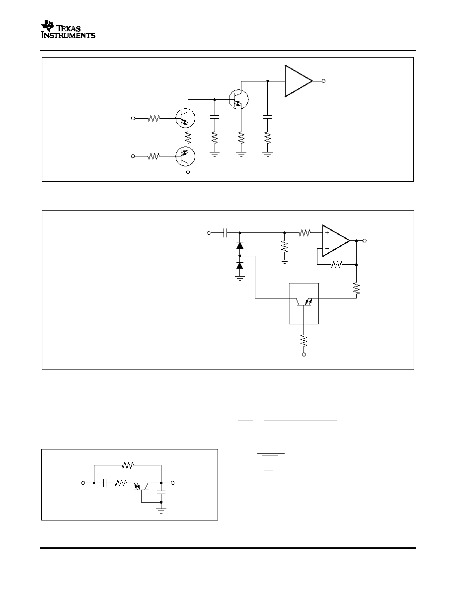
sequent circuit diagrams. Power-supply bypass ca-
pacitors should be located as close as possible to the
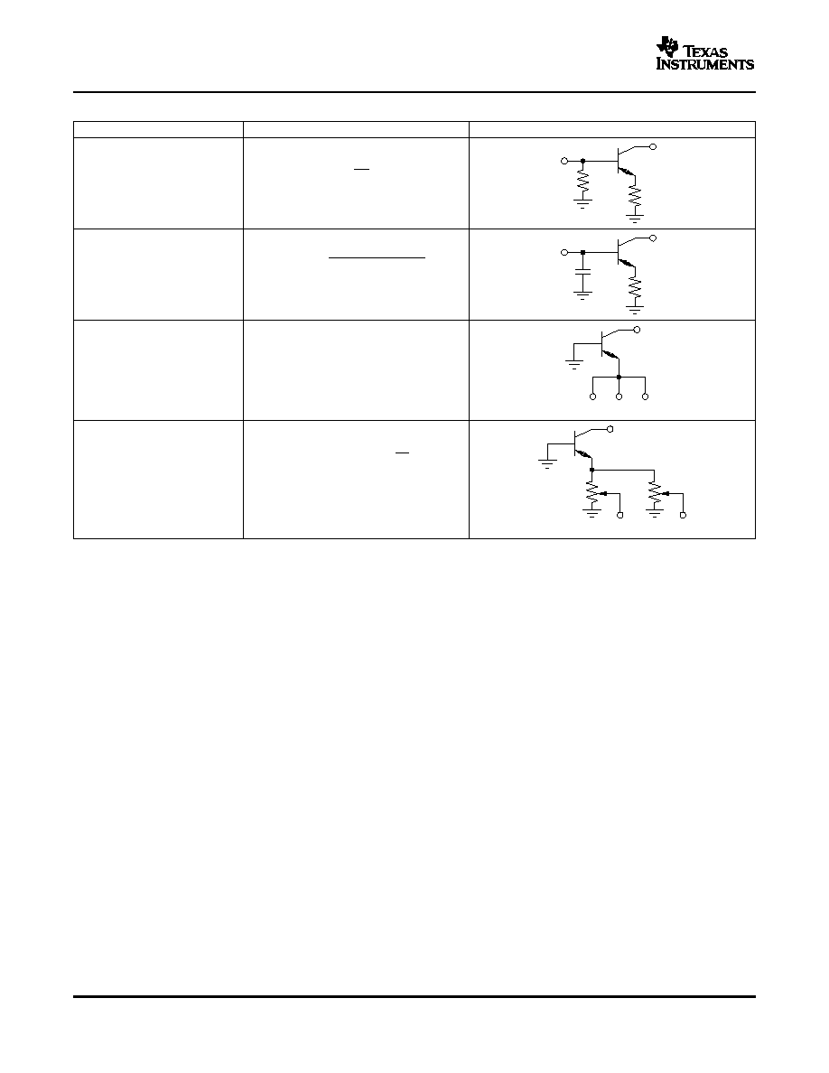
Figure 26. Symbols and Terms
device pins. Solid tantalum capacitors are generally
best.
Regardless of its depiction, the OTA section has a
high-input impedance (B-input), a low-input/output
impedance (E-input), and a high-impedance current
source output (C-output).
Figure 27. Basic Connections
12
www.ti.com
QUIESCENT CURRENT CONTROL PIN
BASIC APPLICATIONS CIRCUITS
Common-E Amplifier or Forward Amplifier
G
+
R
L
1
gm
)
R
E
(1)
R
1
1.25k
TLV2262
OPA861
1/2 REF200
100
µ
A
R
2
425
V+
I
Q
Adjust
1 I
1
OPA861
SBOS338 ≠ AUGUST 2005
With this control loop, quiescent current will be nearly
constant with temperature. Since this method differs
The
quiescent
current
of
the
transconductance
from the temperature-dependent behavior of the
portion of the OPA861 is set with a resistor, R
ADJ
,
internal current source, other temperature-dependent
connected from pin 1 to ≠V
S
. The maximum quiesc-
behavior may differ from that shown in the Typical
ent current is 6mA. R
ADJ
should be set between 50
Characteristics. The circuit of
Figure 28
will control
and 1k
for optimal performance of the OTA section.
the I
Q
of the OPA861 somewhat more accurately than
This range corresponds to the 5mA quiescent current
with a fixed external resistor, R
Q
. Otherwise, there is
for R
ADJ
= 50
, and 1mA for R
ADJ
= 1k
. If the I
Q
no fundamental advantage to using this more com-
adjust pin is connected to the negative supply, the
plex biasing circuitry. It does, however, demonstrate
quiescent current will be set by the 250
internal
the possibility of signal-controlled quiescent current.
resistor.
This capability may suggest other possibilities such
as AGC, dynamic control of AC behavior, or VCO.
Reducing or increasing the quiescent current for the
OTA section controls the bandwidth and AC behavior
as well as the transconductance. With R
ADJ
= 250
,
this sets approximately 5.4mA total quiescent current
Most applications circuits for the OTA section consist
at 25
∞
C. It may be appropriate in some applications to
of a few basic types, which are best understood by
trim this resistor to achieve the desired quiescent
analogy to a transistor. Used in voltage-mode, the
current or AC performance.
OTA section can operate in three basic operating
Applications circuits generally do not show the
states--common emitter, common base, and com-
resistor R
Q
, but it is required for proper operation.
mon collector. In the current-mode, the OTA can be
useful for analog computation such as current ampli-
With a fixed R
ADJ
resistor, quiescent current in-
fier, current differentiator, current integrator, and cur-
creases with temperature (see
Figure 11
in the
rent summer.
Typical Characteristics section). This variation of
current with temperature holds the transconductance,
g
m
, of the OTA relatively constant with temperature
(another advantage over a transistor).
Figure 29
compares the common-emitter configur-
ation for a BJT with the common-E amplifier for the
It is also possible to vary the quiescent current with a
OTA section. There are several advantages in using
control signal. The control loop in
Figure 28
shows
the OTA section in place of a BJT in this configur-
1/2 of a REF200 current source used to develop
ation. Notably, the OTA does not require any biasing,
100mV on R
1
. The loop forces 125mV to appear on
and the transconductance gain remains constant over
R
2
. Total quiescent current of the OPA861 is approxi-
temperature. The output offset voltage is close to 0,
mately 37
◊
I
1
, where I
1
is the current made to flow
compared with several volts for the common-emitter
out of pin 1.
amplifier.
The gain is set in a similar manner as for the BJT
equivalent with
Equation 1
:
Just as transistor circuits often use emitter degener-
ation, OTA circuits may also use degeneration. This
option can be used to reduce the effects that offset
voltage and offset current might otherwise have on
the
DC
operating
point
of
the
OTA.
The
E-degeneration resistor may be bypassed with a
large capacitor to maintain high AC gain. Other
circumstances may suggest a smaller value capacitor
used to extend or optimize high-frequency perform-
ance.
Figure 28. Optional Control Loop for Setting
Quiescent Current
13
www.ti.com
R
1
160
V
I
V
O
3 B
2
E
C
8
R
E
78
R
C
500
G = 5V/V
I
Q
= 5.4mA
OPA861
100
V
I
V+
V
-
V
I
V
O
3 B
2
E
C
8
R
S
R
S
R
L
R
E
V
O
R
E
R
L
Inverting Gain
V
OS
= Several Volts
Noninverting Gain
V
OS
= 0V
(a) Transistor Common-Emitter Amplifier
Transconductance varies over temperature.
(b) OTA Common-E Amplifier
Transconductance remains constant over temperature.
OPA861
g
m_deg
+
1
1
gm
)
R
E
(2)
V
I
V
O
3
2
8
R
E
r
E
R
L2
R
1
100
R
IN
50
R
L
= R
L1
+ R
L2
|| R
IN
OPA861
R
L1
Network
Analyzer
G
+
R
L
R
E
)
r
E
r
E
+
1
g
m
At I
Q
+
5.4mA
r
E
+
1
95mA V
+
10.5
W
G
+
R
L
R
E
)
10.5
W
at I
Q
+
5.4mA
OPA861
SBOS338 ≠ AUGUST 2005
The forward amplifier shown in
Figure 30
and
Fig-
ure 31
corresponds to one of the basic circuits used
to
characterize
the
OPA861.
Extended
characterization of this topology appears in the Typi-
cal Characteristics section of this datasheet.
Figure 30. Forward Amplifier Configuration and
Test Circuit
Figure 29. Common-Emitter vs Common-E
Amplifier
The transconductance of the OTA with degeneration
can be calculated by
Equation 2
:
A positive voltage at the B-input, pin 3, causes a
positive current to flow out of the C-input, pin 8. This
gives a noninverting gain where the circuit of
Fig-
ure 29
a is inverting.
Figure 29
b shows an amplifier
connection of the OPA861, the equivalent of a
common-emitter transistor amplifier. Input and output
can be ground-referenced without any biasing. The
amplifier is non-inverting because of the sense of the
output current.
Figure 31. Forward Amplifier Design Equations
14

www.ti.com
Common-C Amplifier
Current-Mode Analog Computations
G
+
1
1
)
1
gm
R
E
[
1
(3)
G
+
1
1
)
1
gm
R
E
+
1
R
O
+
1
g
m
¯
R
E
100
V
I
3 B
2
E
C
8
G = 1
V
OS
= 0V
G = 1
V
OS
= 0.7V
OPA861
R
E
V
O
(b) OTA Common-C Amplifier
(Buffer)
(a) Transistor Common-Collector Amplifier
(Emitter Follower)
V
O
V
I
R
E
V
-
V+
G
+
R
L
R
E
)
1
gm
+ *
R
L
R
E
(b) OTA Common-B Amplifier
(a) Transistor Common-Base Amplifier
Noninverting Gain
V
OS
= Several Volts
R
E
V
-
V+
V
O
R
L
100
3 B
2
E
C
8
OPA861
R
E
V
-
R
L
Inverting Gain
V
OS
= 0V
V
O
Common-B Amplifier
G
+
R
L
R
E
)
1
gm
[ *
R
L
R
E
(4)
OPA861
SBOS338 ≠ AUGUST 2005
Figure 32
b shows the OPA861 connected as an
As mentioned earlier, the OPA861 can be used
E-follower--a voltage buffer. It is interesting to notice
advantageously for analog computation. Among the
that the larger the R
E
resistor, the closer to unity gain
application possibilities are functionality as a current
the buffer will be. If the OPA861 is to be used as a
amplifier, current differentiator, current integrator, cur-
buffer, use R
E
500
for best results. For the
rent summer, and weighted current summer.
Table 1
OPA861 used as a buffer, the gain is given by
lists these different uses with the associated transfer
Equation 3
:
functions.
These functions can easily be combined to form
active filters. Some examples using these cur-
rent-mode functions are shown later in this document.
Figure 32. Common-Collector vs Common-C
Amplifier
A low value resistor in series with the B-input is
recommended. This resistor helps isolate trace para-
sitic from the inputs, reduces any tendency to oscil-
Figure 33. Common-Base Transistor vs
late, and controls frequency response peaking. Typi-
Common-B OTA
cal resistor values are from 25
to 200
.
Figure 33
shows the Common-B amplifier. This con-
figuration produces an inverting gain and a low
impedance input.
Equation 4
shows the gain for this
configuration.
This low impedance can be converted to a high
impedance by inserting the buffer amplifier in series.
15
www.ti.com
I
OUT
+
R
1
R
2
I
IN
I
OUT
I
IN
R
1
R
2
I
OUT
+
1
C
R
I
IN
dt
I
OUT
I
IN
C
R
I
OUT
+
1
S
n
j
+
1
I
j
I
OUT
I
2
I
n
I
1
I
OUT
+
1
S
n
j
+
1
I
j
R
j
R
I
OUT
I
1
R
R
1
I
n
R
R
n
OPA861 APPLICATIONS
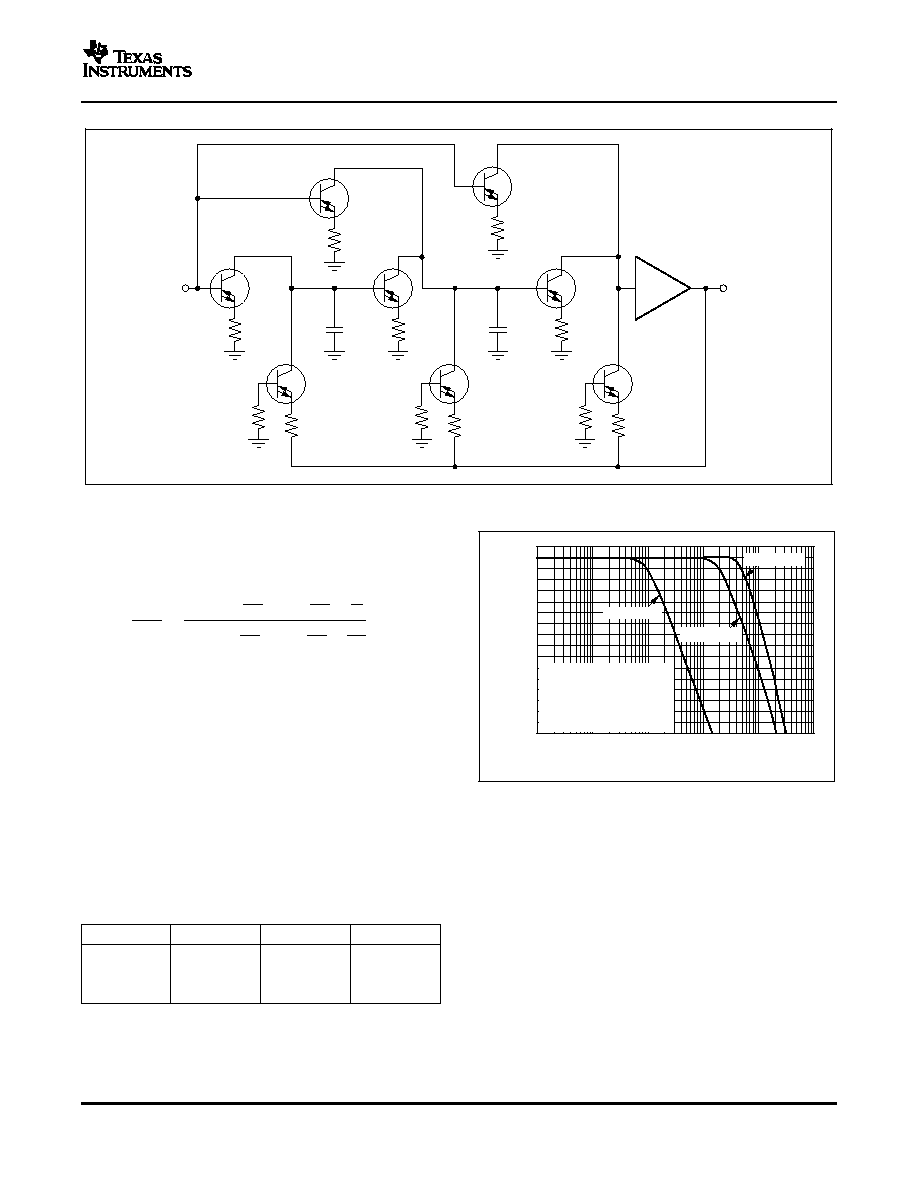
Control-Loop Amplifier
DC-Restore Circuit
OPA861
SBOS338 ≠ AUGUST 2005
Table 1. Current-Mode Analog Computation Using the OTA Section
FUNCTIONAL ELEMENT
TRANSFER FUNCTION
IMPLEMENTATION WITH THE OTA SECTION
Current Amplifier
Current Integrator
Current Summer
Weighted Current Summer
A new type of control loop amplifier for fast and
The OPA861 can be used advantageously with an
precise control circuits can be designed with the
operational
amplifier,
here
the
OPA656,
as
a
OPA861. The circuit of
Figure 34
illustrates a series
DC-restore circuit.
Figure 35
illustrates this design.
connection of two voltage control current sources that
Depending
on
the
collector
current
of
the
have an integral (and at higher frequencies, a pro-
transconductance amplifier (OTA) of the OPA861, a
portional) behavior versus frequency. The control
switching function is realized with the diodes D
1
and
loop amplifiers show an integrator behavior from DC
D
2
.
to the frequency represented by the RC time constant
When the C-output is sourcing current, the capacitor
of the network from the C-output to GND. Above this
C
1
is being charged. When the C-output is sinking
frequency, they operate as an amp with constant
current, D
1
is turned off and D
2
is turned on, letting
gain. The series connection increases the overall gain
the voltage across C
1
be discharged through R
2
.
to about 110dB and thus minimizes the control loop
deviation. The differential configuration at the inputs
The condition to charge C
1
is set by the voltage
enables one to apply the measured output signal and
difference between V
REF
and V
OUT
. For the OTA
the reference voltage to two identical high-impedance
C-output to source current, V
REF
has to be greater
inputs. The output buffer decouples the C-output of
than V
OUT
. The rate of charge of C
1
is set by both R
1
the second OTA in order to insure the AC perform-
and C
1
. The discharge rate is given by R
2
and C
1
.
ance and to drive subsequent output stages.
16
www.ti.com
V
OUT
5
BUF602
6
2
3
33
10pF
10
2
8
10
8
33
10pF
V
IN
180
6
V
REF
180
3
20
20
R
2
100k
V
IN
R
2
100
R
1
40.2
CCII
B
3
2
E
C
8
V
OUT
V
REF
C
1
100pF
D
1
D
2
OPA656
The OTA amplifier works as a current conveyor (CCII) in this circuit, with a current gain of 1.
R
1
and C
1
set the DC restoration time constant.
D
1
adds a propagation delay to the DC restoration.
R
2
and C
1
set the decay time constant.
D
1
, D
2
= 1N4148
R
Q
= 1k
JFET-Input, Wideband
Negative Impedance Converter Filter: Low-Pass
V
OUT
V
IN
+
1
1
)
sC
2
R
)
s
2
C
1
C
2
R
2
(5)
w
0
+
1
C
1
C
2
R
Q
+
C
1
C
2
C
1
C
2
V
IN
R
R
V
OUT
OPA861
SBOS338 ≠ AUGUST 2005
Figure 34. Control-Loop Amplifier Using Three OPA861s
Figure 35. DC Restorer Circuit
The transfer function is shown in
Equation 5
:
Filter
The OPA861 can be used as a negative impedance
converter to realize the low-pass filer shown in
Figure 36
.
with:
Figure 36. Low-Pass Negative Impedance
Converter Filter
17
www.ti.com
Differential Line Driver/Receiver
Z
IN
+
1
2sC
)
R
1
)
sRC
1
)
2sRC
(6)
C
1
+
1
2
C
2
+
5.6
m
F
. For the 10MHz filter, the
0
-
10
-
20
-
30
-
40
-
50
-
60
-
70
-
80
-
90
-
100
Frequency (MHz)
C
o
m
m
o
n
-
M
o
d
e
R
e
j
e
c
t
i
o
n
R
a
t
i
o
(
d
B
c
)
0.001
0.01
0.1
1
10
100
0
-
10
-
20
-
30
-
40
-
50
-
60
-
70
-
80
Frequency (Hz)
G
a
i
n
(
d
B
)
1k
10k
100k
1M
10M
100M
1G
50
50
50
50
V
IN
50
10
100
10
To 50
Load
OPA861
SBOS338 ≠ AUGUST 2005
The input impedance is shown in
Equation 6
:
The wide bandwidth and high slew rate of the
OPA861 current-mode amplifier make it an ideal line
driver. The circuit in
Figure 39
makes use of two
Figure
37
shows
the
frequency
responses
for
OPA861s to realize a single-ended to differential
low-pass, Butterworth filters set at 20kHz and 10MHz.
conversion. The high-impedance current source out-
For
the
20kHz
filter,
set
R
to
1K
and
put of the OPA861 allows it to drive low-impedance or
capacitive loads without series resistances and
avoids any attenuation that would have otherwise
parasitic capacitance at the output pin needs to be
occured in the resistive network.
taken into consideration. In the example of
Figure 37
,
The OPA861 used as a differential receiver exhibits
the parasitic is 3pF, which gives us the settings of R
excellent common-mode rejection ratio, as can be
= 1.13k
, C
1
= 10pF, and C
2
= 17pF.
seen in
Figure 38
.
Figure 38. Differential Driver Common-Mode
Figure 37. Small-Signal Frequency Response for a
Rejection Ratio for 2V
PP
Input Signals
Low-Pass Negative Impedance Converter Filter
Figure 39. Twisted-Pair Differential Driver and Receiver with the OPA861
18
www.ti.com
ACTIVE FILTERS USING THE OPA861 IN
R
V
OUT
C/2
R
+1
C
V
IN
R
I
OUT
C/2
R
CCII
-
C
E
B
C
I
IN
V
OUT
T(s) =
=
=
I
OUT
V
IN
I
IN
s
2
+ 2/RC[2Q(1
-
K) + 1]s + 4KQ
2
/R
2
C
2
4KQ
2
/R
2
C
2
OPA861
SBOS338 ≠ AUGUST 2005
output becomes the input, which is excitated by a
CURRENT CONVEYOR STRUCTURE
current source. The following equation describes the
interreciprocal features of the circuit: V
OUT
/V
IN
=
One further example of the versatility of the Diamond
I
OUT
/I
IN
. Resistances and capacitances remain un-
Transistor
and
Buffer
is
the
construction
of
changed. In the final step, the operational amplifier
high-frequency (> 10MHz) active filters. Here, the
with infinite input impedance and 0
output im-
Current Conveyor structure, shown in
Figure 40
, is
pedance is transformed into a current amplifier with
used with the Diamond Transistor as a Current
0
input impedance and infinite output impedance. A
Conveyor.
Diamond Transistor with the base at ground comes
quite
close
to
an
ideal
current
amplifier.
The
The method of converting RC circuit loops with
well-known Sallen-Key low-pass filter with positive
operational amplifiers in Current Conveyor structures
feedback, is an example of conversion into Cur-
is based upon the adjoint network concept. A network
rent-Conveyor structure, see
Figure 43
. The positive
is reversible or reciprocal when the transfer function
gain of the operational amplifier becomes a negative
does not change even when the input and output
second type of Current Conveyor (CCII), as shown in
have been exchanged. Most networks, of course, are
Figure 40
. Both arrangements have identical transfer
nonreciprocal. The networks of
Figure 41
, perform
functions and the same level of sensitivity to devi-
interreciprocally when the input and output are
ations. The most recent implementation of active
exchanged,
while
the
original
network,
N,
is
filters in a Current-Conveyor structure produced a
exchanged for a new network N
A
. In this case, the
second-order Bi-Quad filter. The value of the resist-
transfer function remains the same, and N
A
is the
ance in the emitter of the Diamond Transistor controls
adjoing network. It is easy to construct an adjoint
the filter characteristic. For more information, refer to
network for any given circuit, and these networks are
application note
SBOS047
, New Ultra High-Speed
the base for circuits in Current-Conveyor structure.
Circuit Techniques with Analog ICs.
Individual elements can be interchanged according to
the list in
Figure 42
. Voltage sources at the input
become short circuits, and the current flowing there
becomes the output variable. In contrast, the voltage
Figure 40. Current Conveyor
19

www.ti.com
N
V
OUT
+
-
N
I
OUT
I
IN
Reciprocal Networks
N
V
OUT
+
-
N
A
I
OUT
I
IN
Interreciprocal Networks
I
IN
V
IN
I
OUT
V
OUT
=
V
IN
V
IN
+
-
µ
V
µ
I
I
C
C
R
R
+
-
V
OUT
V
2
2
2
2
3
4
1
1
1
1
2
2
2
2
3
4
1
1
1
1
1
1
Controlled
Sources
Passive
Elements
Signal
Sources
Element
Adjoint
I
OUT
V
IN
I
IN
OPA861
SBOS338 ≠ AUGUST 2005
Figure 41. Networks
Figure 42. Individual Elements in the Current Conveyor
20
www.ti.com
C
2
R
2M
V
OUT
R
3
R
2S
R
2
R
1S
C
1
V
IN
R
1
R
1M
R
3S
R
B1
R
B2
R
B3
BUF602
Transfer Function
F(p)
+
V
OUT
V
IN
+
s
2
C
1
R
1M
R
2M
R
3
)
sC
1
R
1M
R
2
)
1
R
1
s
2
C
1
R
1M
R
2M
R
3S
)
sC
1
R
1M
R
2S
)
1
R
1S
(7)
Filter Characteristics
3
0
-
3
-
6
-
9
-
12
-
15
-
18
-
21
-
24
-
27
-
30
-
33
-
36
-
39
-
42
-
45
-
48
Frequency (Hz)
G
a
i
n
(
d
B
)
10k
100k
1M
10M
100M
1G
50MHz Filter
20MHz Filter
1MHz Filter
For All Filters:
R
2
= R
3
=
R
1
= R
15
= R
25
= 1/2 R
35
= R
R
1M
= R
2M
= R
0
C
1
= C
2
= C
0
OPA861
SBOS338 ≠ AUGUST 2005
Figure 43. Universal Active Filter
The transfer function of the universal active filter of
Figure 43
is shown in
Equation 7
.
Five filter types can be made with this structure:
∑
For a low-pass filter, set R
2
= R
3
=
,
∑
For a high-pass filter, set R
1
= R
2
=
,
∑
For a bandpass filter, set R
1
= R
3
=
,
∑
For a band rejection filter, set R
2
=
; R
1
= R
3
,
Figure 44. Butterworth Low-Pass Filter with the
∑
For an all-pass filter, set R
1
= R
15
; R
2
= R
25
; and
Universal Active Filter
R
3
= R
35
.
A few designs for a low-pass filter are shown in
The advantages of building active filters using a
Figure 44
and
Table 2
.
Current Conveyor structure are:
∑
The increase in output resistance of operational
Table 2. Component Values for Filters Shown In
amplifiers at high frequencies makes it difficult to
Figure 44
construct feedback filter structures (decrease in
f
O
R
R
O
C
O
stop-band attenuation).
1MHz
150
100
2nF
∑
All filter coefficients are represented by resist-
20MHz
150
100
112.5pF
ances, making it possible to adjust the filter
50MHz
150
100
55pF
frequency response without affecting the filter
coefficients.
21
www.ti.com
High-CMRR, Moderate Precision, Differential
6
3
0
-
3
-
6
-
9
Frequency (Hz)
G
a
i
n
(
d
B
)
1M
10M
100M
1G
5.6dB
75
70
65
60
55
50
45
40
35
30
25
20
Frequency (Hz)
C
o
m
m
o
n
-
M
o
d
e
R
e
j
e
c
t
i
o
n
R
a
t
i
o
(
d
B
)
1k
10k
100k
1M
10M
100M
1G
Input-Referred
600
600
V
IN1
V
CM
V
IN2
R
E
600
ADS5272
OPA861
OPA861
OPA861
SBOS338 ≠ AUGUST 2005
∑
The capacitors which determine the frequency
are located between the ground and the current
source outputs and are thus grounded on one
side. Therefore, all parasitic capacitances can be
viewed as part of these capacitors, making them
easier to comprehend.
∑
The features which determine the frequency
characteristics are currents, which charge the
integration capacitors. This situation is similar to
the transfer characteristic of the Diamond Tran-
sistor.
I/O ADC Driver
The circuit shown in
Figure 45
depicts an ADC driver
implemented with two OPA861s. Since the gain is set
here by the ratio of the internal 600
resistors and
Figure 46. ADC Driver, Small-Signal Frequency
R
E
, its accuracy will only be as good as the input
Response
resistor of the ADS5272. The small-signal frequency
response for this circuit has 150MHz at ≠3dB
bandwidth for a gain of approximately 5.6dB, as
shown in
Figure 46
. The advantage of this circuit lies
in its high CMRR to 100kHz, as shown in
Figure 47
.
This circuit also has more than 10 bits of linearity.
Figure 47. CMRR of the ADC Driver
Figure 45. High CMRR, Moderate Precision, Differ-
ential I/O ADC Driver
22
www.ti.com
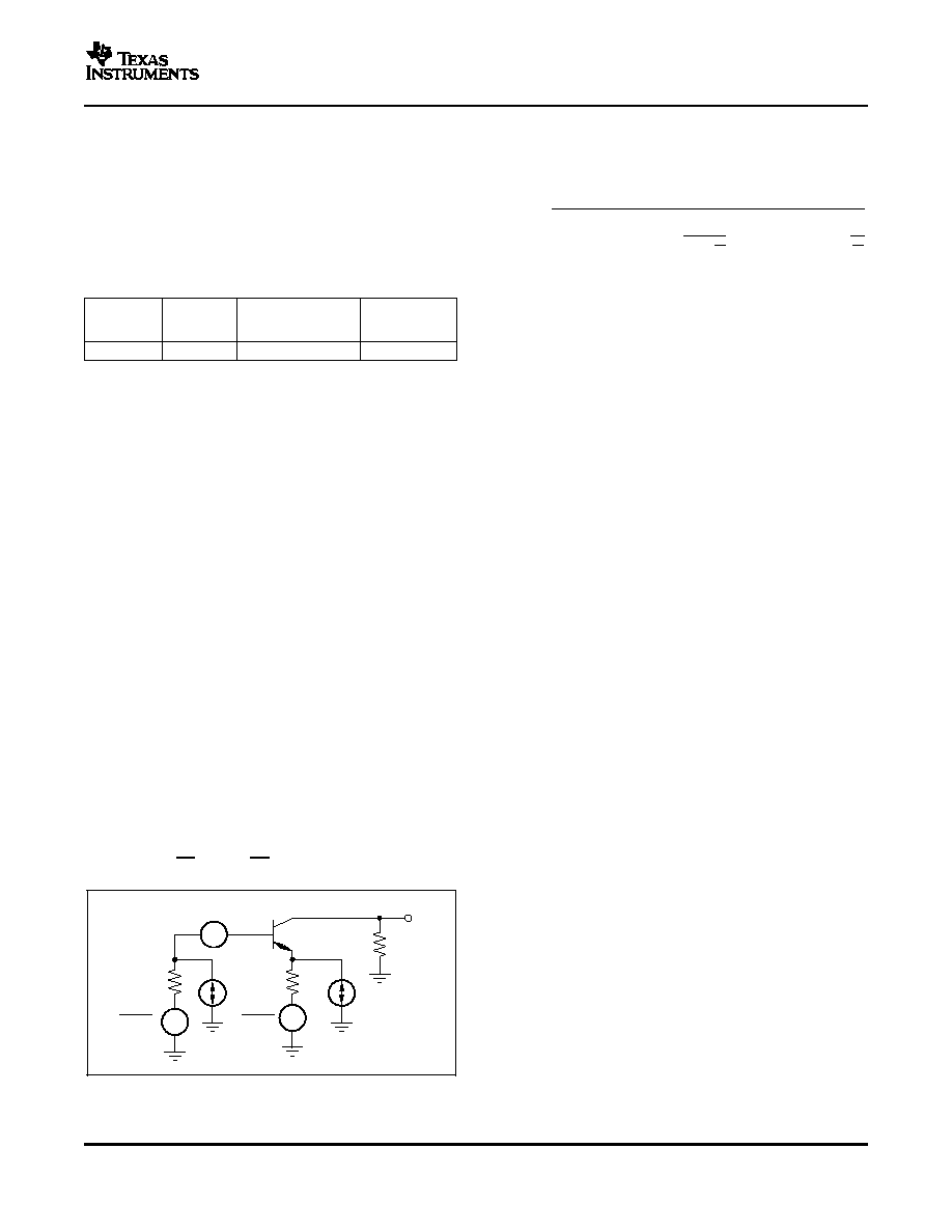
DESIGN-IN TOOLS
DEMONSTRATION BOARDS
e
O
+
e
2
n
)
R
S
i
bn
2
)
4kTR
S
R
L
R
G
)
1
gm
2
)
R
G
i
bi
2
)
4kTR
G
R
L
1
gm
THERMAL ANALYSIS
MACROMODELS AND APPLICATIONS
NOISE PERFORMANCE
BOARD LAYOUT GUIDELINES
e
n
i
bn
i
bi
R
S
R
G
4kTR
S
4kTR
S
R
L
V
O
OPA861
SBOS338 ≠ AUGUST 2005
The total output spot noise voltage can be computed
as the square root of the sum of all squared output
noise voltage contributors.
Equation 8
shows the
general form for the output noise voltage using the
terms shown in
Figure 48
.
A printed circuit board (PCB) is available to assist in
the initial evaluation of circuit performance using the
OPA861. This module is available free, as an
unpopulated PCB delivered with descriptive docu-
mentation. The summary information for the board is
(8)
shown below:
LITERATURE
BOARD PART
REQUEST
PRODUCT
PACKAGE
NUMBER
NUMBER
Maximum desired junction temperature will set the
OPA861ID
SO-8
DEM-OPA86xD
SBOU035
maximum allowed internal power dissipation as de-
scribed below. In no case should the maximum
The board can be requested on Texas Instruments
junction temperature be allowed to exceed 150
∞
C.
web site (
www.ti.com
).
Operating junction temperature (T
J
) is given by
T
A
+ P
D
◊
JA
. The total internal power dissipation
(P
D
) is the sum of quiescent power (P
DQ
) and
SUPPORT
additional power dissipated in the output stage (P
DL
)
Computer simulation of circuit performance using
to deliver output current. Quiescent power is simply
SPICE is often useful when analyzing the perform-
the specified no-load supply current times the total
ance of analog circuits and systems. This principle is
supply voltage across the part. P
DL
will depend on the
particularly true for Video and RF amplifier circuits
required output signal and load but would, for the
where parasitic capacitance and inductance can have
OPA861 be at a maximum when the maximum I
O
is
a major effect on circuit performance. A SPICE model
being driven into a voltage source that puts the
for the OPA861 is available through the Texas
maximum voltage across the output stage. Maximum
Instruments web page (
www.ti.com
). These models
I
O
is 15mA times a 9V maximum across the output.
do a good job of predicting small-signal AC and
Note that it is the power in the output stage and not
transient
performance
under
a
wide
variety
of
into the load that determines internal power dissi-
operating conditions. They do not do as well in
pation.
predicting the harmonic distortion. These models do
not attempt to distinguish between the package types
As a worst-case example, compute the maximum T
J
in their small-signal AC performance.
using an OPA861IDBV in the circuit of
Figure 29
b
operating at the maximum specified ambient tem-
perature of +85
∞
C and driving a ≠1V voltage refer-
ence.
The OTA noise model consists of three elements: a
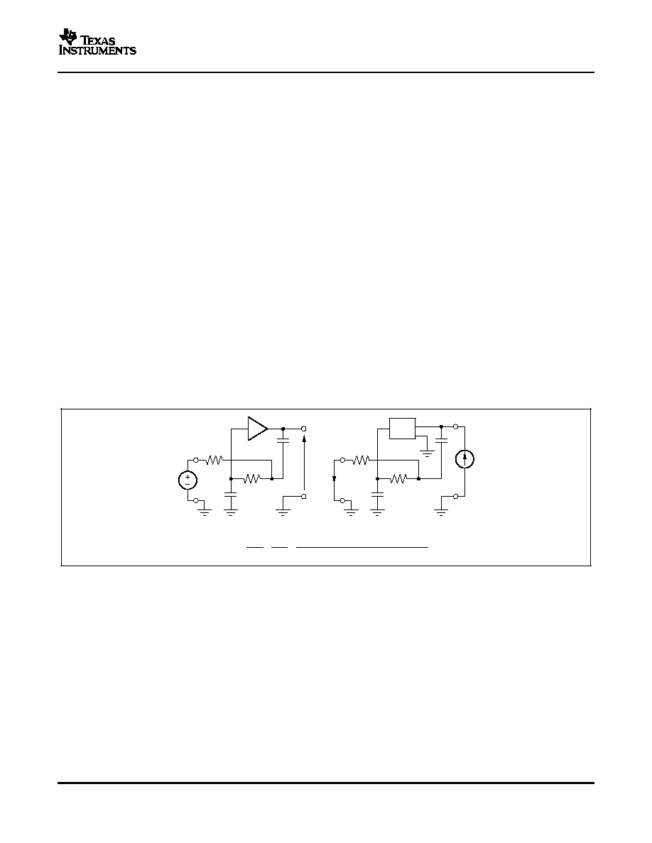
voltage noise on the B-input; a current noise on the
P
D
= 10V
◊
5.4mA + (15mA
◊
9V) = 185mW
B-input; and a current noise on the E-input.
Figure 48
Maximum T
J
= +85
∞
C + (0.19W
◊
150
∞
C/W) = 114
∞
C.
shows the OTA noise analysis model with all the
noise terms included. In this model, all noise terms
Although this is still well below the specified maxi-
are taken to be noise voltage or current density terms
mum junction temperature, system reliability con-
in either nV/
Hz or pA/
Hz.
siderations may require lower tested junction tem-
peratures. The highest possible internal dissipation
will occur if the load requires current to be forced into
the output for positive output voltages or sourced
from the output for negative output voltages. This
puts a high current through a large internal voltage
drop in the output transistors.
Achieving
optimum
performance
with
a
high-frequency amplifier like the OPA861 requires
careful attention to board layout parasitics and exter-
Figure 48. OTA Noise Analysis Model
nal component types. Recommendations that will
optimize performance include:
23
www.ti.com
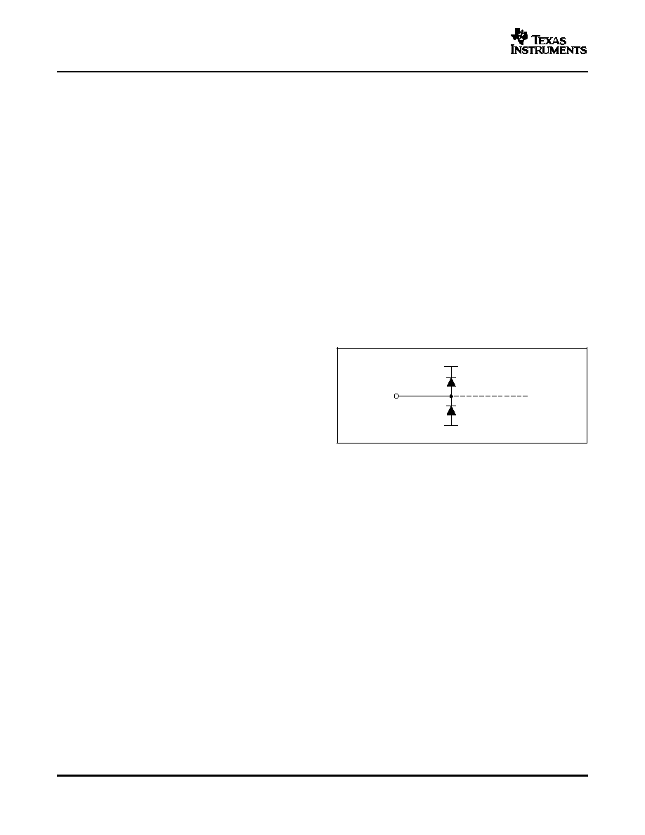
INPUT AND ESD PROTECTION
External
Pin
+V
CC
-
V
CC
Internal
Circuitry
OPA861
SBOS338 ≠ AUGUST 2005
a) Minimize parasitic capacitance to any AC ground
nections, consider the trace and the input to the next
for all of the signal I/O pins. Parasitic capacitance on
device as a lumped capacitive load. Relatively wide
the inverting input pin can cause instability: on the
traces (50mils to 100mils) should be used, preferably
noninverting input, it can react with the source im-
with ground and power planes opened up around
pedance to cause unintentional bandlimiting. To re-
them.
duce unwanted capacitance, a window around the
e) Socketing a high-speed part like the OPA861 is
signal I/O pins should be opened in all of the ground
not recommended. The additional lead length and
and power planes around those pins. Otherwise,
pin-to-pin capacitance introduced by the socket can
ground and power planes should be unbroken else-
create an extremely troublesome parasitic network
where on the board.
that makes it almost impossible to achieve a smooth,
b) Minimize the distance (< 0.25") from the
stable frequency response. Best results are obtained
power-supply pins to high-frequency 0.1µF decoup-
by soldering the OPA861 onto the board.
ling capacitors. At the device pins, the ground and
power-plane layout should not be in close proximity to
the signal I/O pins. Avoid narrow power and ground
The OPA861 is built using a very high-speed comp-
traces to minimize inductance between the pins and
lementary bipolar process. The internal junction
the decoupling capacitors. The power-supply connec-
breakdown voltages are relatively low for these very
tions should always be decoupled with these capaci-
small geometry devices. These breakdowns are re-
tors. An optional supply decoupling capacitor (0.1µF)
flected in the Absolute Maximum Ratings table. All
across the two power supplies (for bipolar operation)
device pins are protected with internal ESD protection
will improve 2nd-harmonic distortion performance.
diodes to the power supplies as shown in
Figure 49
.
Larger (2.2µF to 6.8µF) decoupling capacitors, effec-
tive at lower frequency, should also be used on the
main supply pins. These may be placed somewhat
farther from the device and may be shared among
several devices in the same area of the PC board.
c) Careful selection and placement of external
components will preserve the high-frequency per-
formance of the OPA861. Resistors should be a
very low reactance type. Surface-mount resistors
work best and allow a tighter overall layout. Metal film
or carbon composition, axially-leaded resistors can
Figure 49. Internal ESD Protection
also
provide
good
high-frequency
performance.
Again, keep their leads and PC board traces as short
These diodes provide moderate protection to input
as possible. Never use wirewound type resistors in a
overdrive voltages above the supplies as well. The
high-frequency application.
protection diodes can typically support 30mA continu-
ous current. Where higher currents are possible (for
d) Connections to other wideband devices on the
example, in systems with
±
15V supply parts driving
board may be made with short, direct traces or
into the OPA861), current-limiting series resistors
through onboard transmission lines. For short con-
should be added into the two inputs. Keep these
resistor values as low as possible since high values
degrade both noise performance and frequency re-
sponse.
24

PACKAGING INFORMATION
Orderable Device
Status
(1)
Package
Type
Package
Drawing
Pins Package
Qty
Eco Plan
(2)
Lead/Ball Finish
MSL Peak Temp
(3)
OPA861ID
ACTIVE
SOIC
D
8
75
TBD
Call TI
Call TI
OPA861IDBVR
ACTIVE
SOT-23
DBV
6
3000
TBD
Call TI
Call TI
OPA861IDBVT
ACTIVE
SOT-23
DBV
6
250
TBD
Call TI
Call TI
OPA861IDR
ACTIVE
SOIC
D
8
2500
TBD
Call TI
Call TI
(1)
The marketing status values are defined as follows:
ACTIVE: Product device recommended for new designs.
LIFEBUY: TI has announced that the device will be discontinued, and a lifetime-buy period is in effect.
NRND: Not recommended for new designs. Device is in production to support existing customers, but TI does not recommend using this part in
a new design.
PREVIEW: Device has been announced but is not in production. Samples may or may not be available.
OBSOLETE: TI has discontinued the production of the device.
(2)
Eco
Plan
-
The
planned
eco-friendly
classification:
Pb-Free
(RoHS)
or
Green
(RoHS
&
no
Sb/Br)
-
please
check
http://www.ti.com/productcontent
for the latest availability information and additional product content details.
TBD: The Pb-Free/Green conversion plan has not been defined.
Pb-Free (RoHS): TI's terms "Lead-Free" or "Pb-Free" mean semiconductor products that are compatible with the current RoHS requirements
for all 6 substances, including the requirement that lead not exceed 0.1% by weight in homogeneous materials. Where designed to be soldered
at high temperatures, TI Pb-Free products are suitable for use in specified lead-free processes.
Green (RoHS & no Sb/Br): TI defines "Green" to mean Pb-Free (RoHS compatible), and free of Bromine (Br) and Antimony (Sb) based flame
retardants (Br or Sb do not exceed 0.1% by weight in homogeneous material)
(3)
MSL, Peak Temp. -- The Moisture Sensitivity Level rating according to the JEDEC industry standard classifications, and peak solder
temperature.
Important Information and Disclaimer:The information provided on this page represents TI's knowledge and belief as of the date that it is
provided. TI bases its knowledge and belief on information provided by third parties, and makes no representation or warranty as to the
accuracy of such information. Efforts are underway to better integrate information from third parties. TI has taken and continues to take
reasonable steps to provide representative and accurate information but may not have conducted destructive testing or chemical analysis on
incoming materials and chemicals. TI and TI suppliers consider certain information to be proprietary, and thus CAS numbers and other limited
information may not be available for release.
In no event shall TI's liability arising out of such information exceed the total purchase price of the TI part(s) at issue in this document sold by TI
to Customer on an annual basis.
PACKAGE OPTION ADDENDUM
www.ti.com
27-Sep-2005
Addendum-Page 1
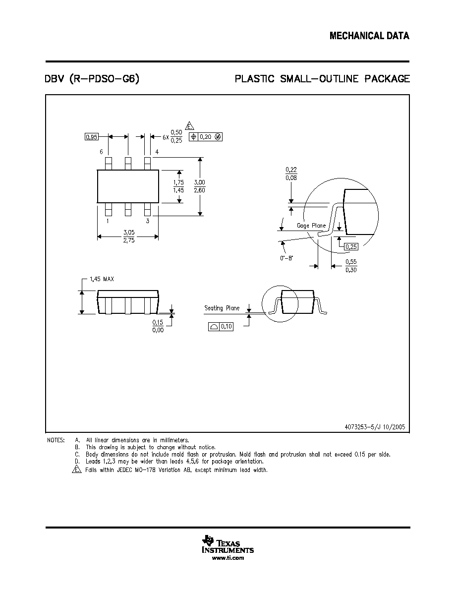
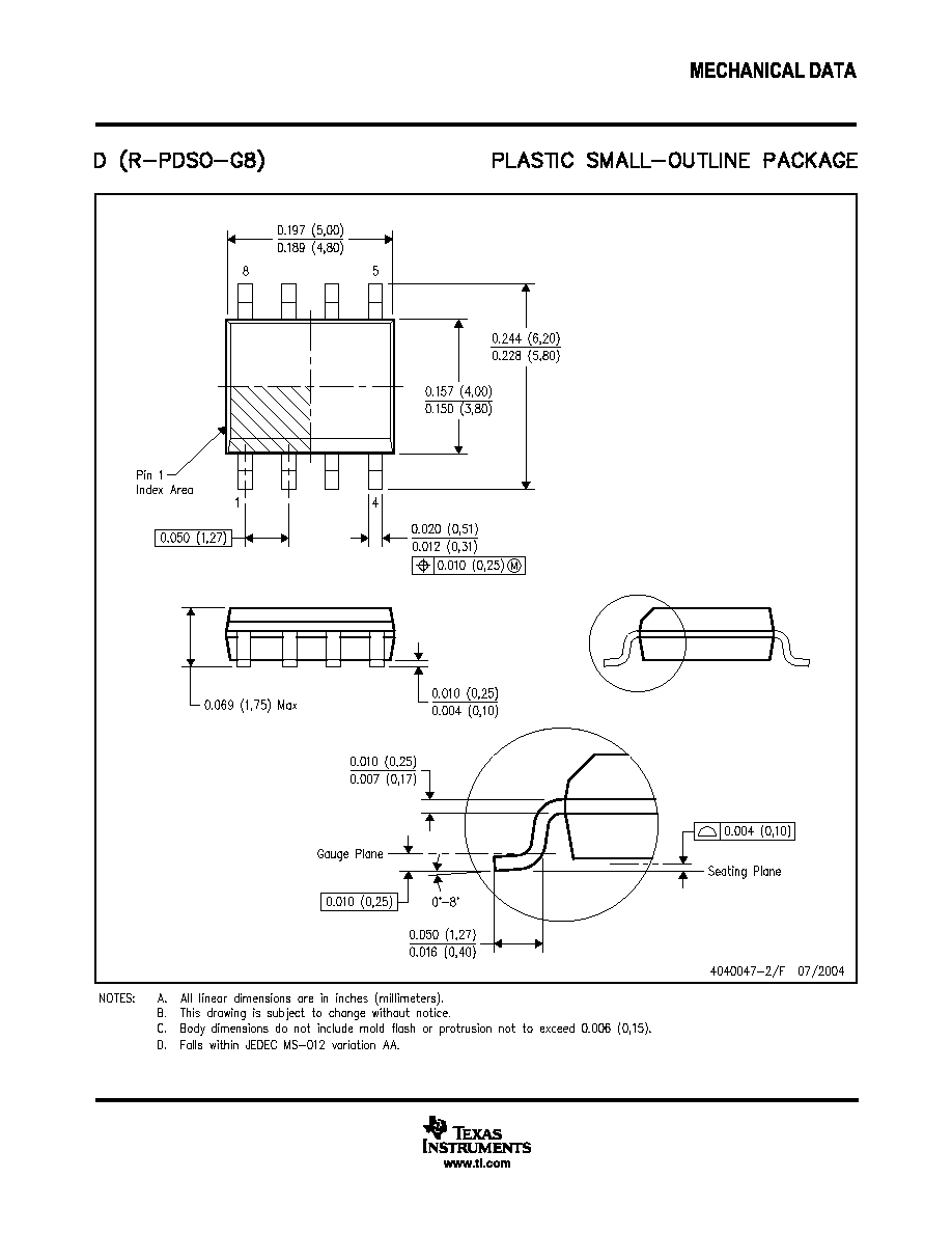

IMPORTANT NOTICE
Texas Instruments Incorporated and its subsidiaries (TI) reserve the right to make corrections, modifications,
enhancements, improvements, and other changes to its products and services at any time and to discontinue
any product or service without notice. Customers should obtain the latest relevant information before placing
orders and should verify that such information is current and complete. All products are sold subject to TI's terms
and conditions of sale supplied at the time of order acknowledgment.
TI warrants performance of its hardware products to the specifications applicable at the time of sale in
accordance with TI's standard warranty. Testing and other quality control techniques are used to the extent TI
deems necessary to support this warranty. Except where mandated by government requirements, testing of all
parameters of each product is not necessarily performed.
TI assumes no liability for applications assistance or customer product design. Customers are responsible for
their products and applications using TI components. To minimize the risks associated with customer products
and applications, customers should provide adequate design and operating safeguards.
TI does not warrant or represent that any license, either express or implied, is granted under any TI patent right,
copyright, mask work right, or other TI intellectual property right relating to any combination, machine, or process
in which TI products or services are used. Information published by TI regarding third-party products or services
does not constitute a license from TI to use such products or services or a warranty or endorsement thereof.
Use of such information may require a license from a third party under the patents or other intellectual property
of the third party, or a license from TI under the patents or other intellectual property of TI.
Reproduction of information in TI data books or data sheets is permissible only if reproduction is without
alteration and is accompanied by all associated warranties, conditions, limitations, and notices. Reproduction
of this information with alteration is an unfair and deceptive business practice. TI is not responsible or liable for
such altered documentation.
Resale of TI products or services with statements different from or beyond the parameters stated by TI for that
product or service voids all express and any implied warranties for the associated TI product or service and
is an unfair and deceptive business practice. TI is not responsible or liable for any such statements.
Following are URLs where you can obtain information on other Texas Instruments products and application
solutions:
Products
Applications
Amplifiers
amplifier.ti.com
Audio
www.ti.com/audio
Data Converters
dataconverter.ti.com
Automotive
www.ti.com/automotive
DSP
dsp.ti.com
Broadband
www.ti.com/broadband
Interface
interface.ti.com
Digital Control
www.ti.com/digitalcontrol
Logic
logic.ti.com
Military
www.ti.com/military
Power Mgmt
power.ti.com
Optical Networking
www.ti.com/opticalnetwork
Microcontrollers
microcontroller.ti.com
Security
www.ti.com/security
Telephony
www.ti.com/telephony
Video & Imaging
www.ti.com/video
Wireless
www.ti.com/wireless
Mailing Address:
Texas Instruments
Post Office Box 655303 Dallas, Texas 75265
Copyright
2005, Texas Instruments Incorporated