 | –≠–ª–µ–∫—Ç—Ä–æ–Ω–Ω—ã–π –∫–æ–º–ø–æ–Ω–µ–Ω—Ç: OPT101P-J | –°–∫–∞—á–∞—Ç—å:  PDF PDF  ZIP ZIP |
Document Outline
- FEATURES
- APPLICATIONS
- DESCRIPTION
- SPECIFICATIONS
- PHOTODIODE SPECIFICATIONS
- OP AMP SPECIFICATIONS
- PACKAGE/ORDERING INFORMATION(
- PIN CONFIGURATIONS
- ABSOLUTE MAXIMUM RATINGS(
- TYPICAL PERFORMANCE CURVES
- APPLICATIONS INFORMATION
- CAPACITIVE LOADING
- NOISE PERFORMANCE
- DARK ERRORS
- CHANGING RESPONSIVITY
- LIGHT SOURCE POSITIONING
- DYNAMIC RESPONSE
- LINEARITY PERFORMANCE
SPECTRAL RESPONSIVITY
Wavelength (nm)
200
300
400
500
600
700
800
900
1000 1100
Voltage Output (V/µW)
Using Internal
1M
Resistor
Infrared
Ultraviolet
Blue
Green
Yellow
Red
0.7
0.6
0.5
0.4
0.3
0.2
0.1
0
0.7
0.6
0.5
0.4
0.3
0.2
0.1
0
Photodiode Responsivity (A/W)
OPT101
FEATURES
q
SINGLE SUPPLY: +2.7 to +36V
q
PHOTODIODE SIZE: 0.090 x 0.090 inch
q
INTERNAL 1M
FEEDBACK RESISTOR
q
HIGH RESPONSIVITY: 0.45A/W
(650nm)
q
BANDWIDTH: 14kHz at R
F
= 1M
q
LOW QUIESCENT CURRENT: 120
µ
A
q
AVAILABLE IN 8-PIN DIP AND 8-LEAD
SURFACE-MOUNT PACKAGES
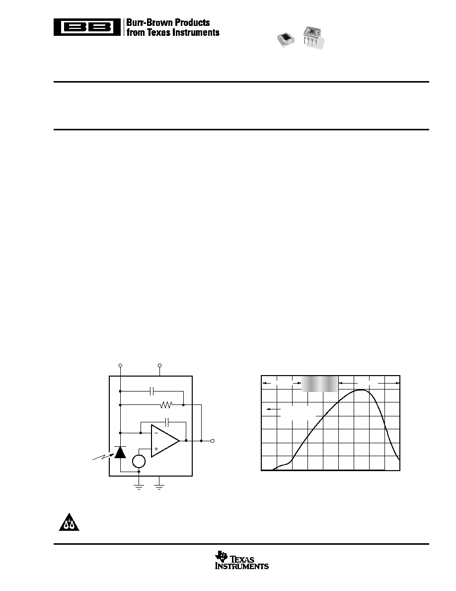
MONOLITHIC PHOTODIODE AND
SINGLE-SUPPLY TRANSIMPEDANCE AMPLIFIER
1M
OPT101
3pF
8pF
2
5
4
V+
3
8
V
B
7.5mV
1
DESCRIPTION
The OPT101 is a monolithic photodiode with on-chip
transimpedance amplifier. Output voltage increases linearly
with light intensity. The amplifier is designed for single or
dual power-supply operation, making it ideal for battery-
operated equipment.
The integrated combination of photodiode and
transimpedance amplifier on a single chip eliminates the
problems commonly encountered in discrete designs such as
leakage current errors, noise pick-up, and gain peaking due
to stray capacitance. The 0.09 x 0.09 inch photodiode is
operated in the photoconductive mode for excellent linearity
and low dark current.
The OPT101 operates from +2.7V to +36V supplies and
quiescent current is only 120
µ
A. It is available in clear
plastic 8-pin DIP, and J-formed DIP for surface mounting.
Temperature range is 0
∞
C to +70
∞
C.
APPLICATIONS
q
MEDICAL INSTRUMENTATION
q
LABORATORY INSTRUMENTATION
q
POSITION AND PROXIMITY SENSORS
q
PHOTOGRAPHIC ANALYZERS
q
BARCODE SCANNERS
q
SMOKE DETECTORS
q
CURRENCY CHANGERS
SBBS002A ≠ JANUARY 1994 ≠ REVISED OCTOBER 2003
www.ti.com
PRODUCTION DATA information is current as of publication date.
Products conform to specifications per the terms of Texas Instruments
standard warranty. Production processing does not necessarily include
testing of all parameters.
Copyright © 1994-2003, Texas Instruments Incorporated
Please be aware that an important notice concerning availability, standard warranty, and use in critical applications of
Texas Instruments semiconductor products and disclaimers thereto appears at the end of this data sheet.
All trademarks are the property of their respective owners.
OPT101
2
SBBS002A
www.ti.com
SPECIFICATIONS
At T
A
= +25
∞
C, V
S
= +2.7V to +36V,
= 650nm, internal 1M
feedback resistor, and R
L
= 10k
,
unless otherwise noted.
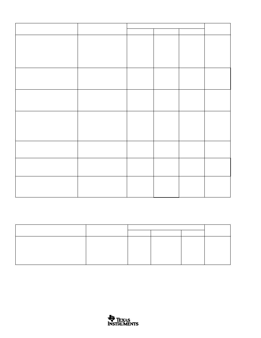
PHOTODIODE SPECIFICATIONS
T
A
= +25
∞
C, V
S
= +2.7V to +36V unless otherwise noted.
Photodiode of OPT101P
PARAMETER
CONDITIONS
MIN
TYP
MAX
UNITS
Photodiode Area
(0.090
x
0.090in)
0.008
in
2
(2.29
x
2.29mm)
5.2
mm
2
Current Responsivity
650nm
0.45
A/W
650nm
865
µ
A/W/cm
2
Dark Current
V
DIODE
= 7.5mV
2.5
pA
vs Temperature
Doubles every 7
∞
C
Capacitance
1200
pF
OPT101P
PARAMETER
CONDITIONS
MIN
TYP
MAX
UNITS
RESPONSIVITY
Photodiode Current
650nm
0.45
A/W
Voltage Output
650nm
0.45
V/
µ
W
vs Temperature
100
ppm/
∞
C
Unit to Unit Variation
650nm
±
5
%
Nonlinearity
(1)
FS Output = 24V
±
0.01
% of FS
Photodiode Area
(0.090 x 0.090in)
0.008
in
2
(2.29 x 2.29mm)
5.2
mm
2
DARK ERRORS, RTO
(2)
Offset Voltage, Output
+5
+7.5
+10
mV
vs Temperature
±
10
µ
V/
∞
C
vs Power Supply
V
S
= +2.7V to +36V
10
100
µ
V/V
Voltage Noise, Dark, f
B
= 0.1Hz to 20kHz
V
S
= +15V, V
PIN3
= ≠15V
300
µ
Vrms
TRANSIMPEDANCE GAIN
Resistor
1
M
Tolerance, P
±
0.5
±
2
%
W
±
0.5
%
vs Temperature
±
50
ppm/
∞
C
FREQUENCY RESPONSE
Bandwidth
V
OUT
= 10Vp-p
14
kHz
Rise Fall Time, 10% to 90%
V
OUT
= 10V Step
28
µ
s
Settling Time, 0.05%
V
OUT
= 10V Step
160
µ
s
0.1%
80
µ
s
1%
70
µ
s
Overload Recovery
100%, Return to Linear Operation
50
µ
s
OUTPUT
Voltage Output, High
(V
S
) ≠ 1.3
(V
S
) ≠ 1.15
V
Capacitive Load, Stable Operation
10
nF
Short-Circuit Current
V
S
= 36V
15
mA
POWER SUPPLY
Operating Voltage Range
+2.7
+36
V
Quiescent Current
Dark, V
PIN3
= 0V
120
240
µ
A
R
L
=
, V
OUT
= 10V
220
µ
A
TEMPERATURE RANGE
Specification
0
+70
∞
C
Operating
0
+70
∞
C
Storage
≠25
+85
∞
C
Thermal Resistance,
JA
100
∞
C/W
NOTES: (1) Deviation in percent of full scale from best-fit straight line. (2) Referred to Output. Includes all error sources.
OPT101
3
SBBS002A
www.ti.com
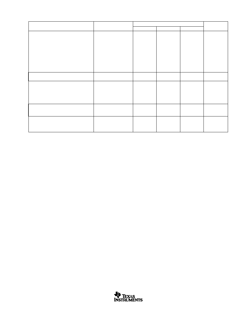
OP AMP SPECIFICATIONS
At T
A
= +25
∞
C, V
S
= +2.7V to +36V,
= 650nm, internal 1M
feedback resistor, and R
L
= 10k
,
unless otherwise noted.
OPT101 Op Amp
(1)
PARAMETER
CONDITIONS
MIN
TYP
MAX
UNITS
INPUT
Offset Voltage
±
0.5
mV
vs Temperature
±
2.5
µ
V/
∞
C
vs Power Supply
10
µ
V/V
Input Bias Current
(≠) Input
165
pA
vs Temperature
(≠) Input
Doubles every 10
∞
C
Input Impedance
Differential
400 || 5
M
|| pF
Common-Mode
250 || 35
G
|| pF
Common-Mode Input Voltage Range
Linear Operation
0 to [(V
S
) ≠ 1]
V
Common-Mode Rejection
90
dB
OPEN-LOOP GAIN
Open-loop Voltage Gain
90
dB
FREQUENCY RESPONSE
Gain-Bandwidth Product
(2)
2
MHz
Slew Rate
1
V/
µ
s
Settling Time 1%
5.8
µ
s
0.1%
7.7
µ
s
0.05%
8.0
µ
s
OUTPUT
Voltage Output, High
(V
S
)
≠ 1.3
(V
S
) ≠ 1.15
V
Short-Circuit Current
V
S
= +36V
15
mA
POWER SUPPLY
Operating Voltage Range
+2.7
+36
V
Quiescent Current
Dark, V
PIN3
= 0V
120
240
µ
A
R
L
=
, V
OUT
= 10V
220
µ
A
NOTES: (1) Op amp specifications provided for information and comparison only. (2) Stable gains
10V/V.
OPT101
4
SBBS002A
www.ti.com
MOISTURE SENSITIVITY
AND SOLDERING
Clear plastic does not contain the structural-enhancing fillers
used in black plastic molding compound. As a result, clear
plastic is more sensitive to environmental stress than black
plastic. This can cause difficulties if devices have been stored
in high humidity prior to soldering. The rapid heating during
soldering can stress wire bonds and cause failures. Prior to
soldering, it is recommended that plastic devices be baked-out
at +85
∞
C for 24 hours.
The fire-retardant fillers used in black plastic are not compat-
ible with clear molding compound. The OPT101 plastic
packages cannot meet flammability test, UL-94.
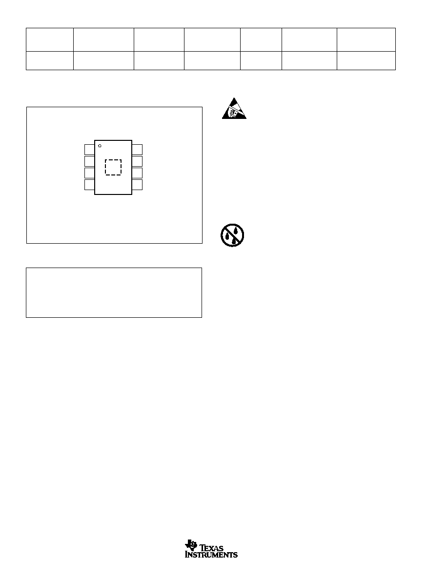
PIN CONFIGURATIONS
Top View
DIP
V
S
≠In
≠V
1M
Feedback
Common
NC
NC
Output
1
2
3
4
8
7
6
5
(1)
NOTE: (1) Photodiode location.
ABSOLUTE MAXIMUM RATINGS
(1)
Supply Voltage (V
S
to
"Common" or pin 3) ................................ 0 to +36V
Output Short-Circuit (to ground) ............................................... Continuous
Operating Temperature .................................................... ≠25
∞
C to +85
∞
C
Storage Temperature ........................................................ ≠25
∞
C to +85
∞
C
Junction Temperature ...................................................................... +85
∞
C
Lead Temperature (soldering, 10s) ............................................... +300
∞
C
(Vapor-Phase Soldering Not Recommended)
NOTE: (1) Stresses above these ratings may cause permanent damage.
Exposure to absolute maximum conditions for extended periods may degrade
device reliability. These are stress ratings only, and functional operation of the
device at these or any other conditions beyond those specified is not implied.
ELECTROSTATIC
DISCHARGE SENSITIVITY
This integrated circuit can be damaged by ESD. Texas
Instruments recommends that all integrated circuits be handled
with appropriate precautions. Failure to observe proper han-
dling and installation procedures can cause damage.
ESD damage can range from subtle performance degradation
to complete device failure. Precision integrated circuits may
be more susceptible to damage because very small parametric
changes could cause the device not to meet its published
specifications.
SPECIFIED
PACKAGE
TEMPERATURE
PACKAGE
ORDERING
TRANSPORT
PRODUCT
PACKAGE-LEAD
DESIGNATOR
RANGE
MARKING
NUMBER
MEDIA, QUANTITY
OPT101P
DIP-8
NTC
≠25
∞
C to +85
∞
C
OPT101
OPT101P
Rail, 50
OPT101P-J
DIP-8, Surface Mount
(2)
DTL
≠25
∞
C to +85
∞
C
OPT101
OPT101P-J
Rail, 50
NOTES: (1) For the most current package and ordering information, see the Package Option Addendum at the end of this data sheet. (2) 8-pin DIP with J-formed
leads for surface mounting.
PACKAGE/ORDERING INFORMATION
(1)
OPT101
5
SBBS002A
www.ti.com
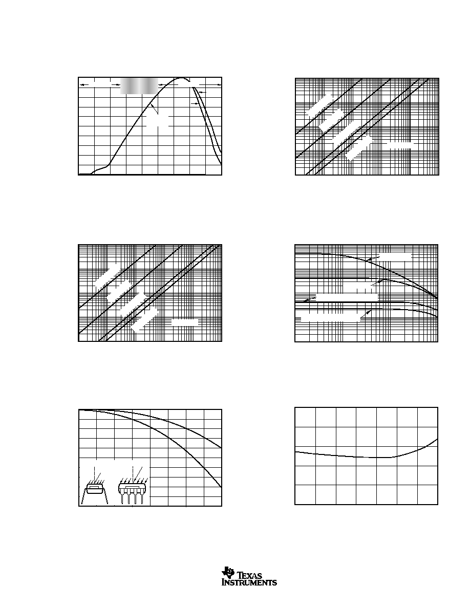
TYPICAL PERFORMANCE CURVES
At T
A
= +25
∞
C, V
S
= +2.7V to +36V,
= 650nm, internal 1M
feedback resistor, and R
L
= 10k
,
unless otherwise noted.
VOLTAGE RESPONSIVITY vs RADIANT POWER
Radiant Power (µW)
Output Voltage (V)
0.01
0.1
10
100
1k
1
10
1
0.1
0.01
0.001
R
F
= 1M
R
F
= 100k
R
F
= 10M
= 650nm
R
F
= 50k
RESPONSE vs INCIDENT ANGLE
Relative Response
Incident Angle (
∞
)
0
1.0
0.8
0.6
0.4
0.2
0
±
20
±
40
±
60
±
80
Y
X
1.0
0.8
0.6
0.4
0.2
0
Y
X
Plastic
DIP Package
DARK V
OUT
vs TEMPERATURE
Temperature (
∞
C)
0
10
20
30
40
50
60
70
8
7.8
7.6
7.4
7.2
7
Output Voltage (mV)
VOLTAGE RESPONSIVITY vs IRRADIANCE
Irradiance (W/m
2
)
Output Voltage (V)
0.001
0.01
1
10
100
0.1
10
1
0.1
0.01
0.001
R
F
= 1M
R
F
= 100k
R
F
= 10M
= 650nm
R
F
= 50k
VOLTAGE RESPONSIVITY vs FREQUENCY
Frequency (Hz)
100
1k
10k
100k
10
1
0.1
0.01
0.001
Responsivity (V/µW)
R
F
= 50k
, C
EXT
= 56pF
R
F
= 10M
R
F
= 1M
R
F
= 100k
, C
EXT
= 33pF
NORMALIZED SPECTRAL RESPONSIVITY
Wavelength (nm)
200
300
400
500
600
700
800
900
1000 1100
1.0
0.9
0.8
0.7
0.6
0.5
0.4
0.3
0.2
0.1
0
Normalized Current or Voltage Output
Ultraviolet
Blue
Green
Yellow
Red
70∞C
25∞C
Infrared
650nm
(0.45A/W)