 | –≠–ª–µ–∫—Ç—Ä–æ–Ω–Ω—ã–π –∫–æ–º–ø–æ–Ω–µ–Ω—Ç: PCA8550D | –°–∫–∞—á–∞—Ç—å:  PDF PDF  ZIP ZIP |

PCA8550
NONVOLATILE 5-BIT REGISTER
WITH I
2
C INTERFACE
SCPS050A ≠ MARCH 1999 ≠ REVISED APRIL 1999
1
POST OFFICE BOX 655303
∑
DALLAS, TEXAS 75265
D
EPIC
TM
(Enhanced-Performance Implanted
CMOS) Submicron Process
D
Useful for Jumperless Configuration of PC
Motherboard
D
Inputs Accept Voltages to 5.5 V
D
MUX OUT Signals are 2.5-V Outputs
D
NON-MUXED OUT Signal is a 3.3-V Output
D
Minimum of 1000 Write Cycles
D
Minimum of 10 Years Data Retention
D
Package Options Include Plastic
Small-Outline (D), Shrink Small-Outline
(DB), and Thin Shrink Small-Outline (PW)
Packages
description
This 4-bit 1-of-2 multiplexer with I
2
C input interface is designed for 3-V to 3.6-V V
CC
operation.
The PCA8550 is designed to multiplex four bits of data from parallel inputs or from I
2
C input data stored in a
nonvolatile register. An additional bit of register output also is provided, which is latched to prevent changes in
the output value during the write cycle. The factory default for the contents of the register is all low. These stored
values can be read from, or written to, using the I
2
C bus. The ability to control writing to the register is provided
by the write protect (WP) input. The override (OVERRIDE) input forces all the register outputs to a low.
This device provides a fast-mode (400 kbit/s) or standard-mode (100 kbit/s) I
2
C serial interface for data input
and output. The implementation is as a slave. The device address is specified in the I
2
C interface definition table.
Both of the I
2
C Schmitt-trigger inputs (SCL and SDA) provide integrated pullup resistors and are 5-V tolerant.
The PCA8550 is characterized for operation from 0
∞
C to 70
∞
C.
FUNCTION TABLE
INPUTS
OUTPUTS
MUX SELECT
OVERRIDE
MUX OUT
NON-MUXED
OUT
L
L
L
L
L
H
Nonvolatile
register
Nonvolatile
register
H
X
MUX IN
Latched
NON-MUXED
OUT
The latched NON-MUXED OUT state is the value present on the
NON-MUXED OUT output at the time the MUX SELECT input
transitions from the low to the high state.
Copyright
©
1999, Texas Instruments Incorporated
PRODUCTION DATA information is current as of publication date.
Products conform to specifications per the terms of Texas Instruments
standard warranty. Production processing does not necessarily include
testing of all parameters.
Please be aware that an important notice concerning availability, standard warranty, and use in critical applications of
Texas Instruments semiconductor products and disclaimers thereto appears at the end of this data sheet.
EPIC is a trademark of Texas Instruments Incorporated.
1
2
3
4
5
6
7
8
16
15
14
13
12
11
10
9
I
2
C SCL
I
2
C SDA
OVERRIDE
MUX IN A
MUX IN B
MUX IN C
MUX IN D
GND
V
CC
WP
NON-MUXED OUT
MUX SELECT
MUX OUT A
MUX OUT B
MUX OUT C
MUX OUT D
D, DB, OR PW PACKAGE
(TOP VIEW)
PCA8550
NONVOLATILE 5-BIT REGISTER
WITH I
2
C INTERFACE
SCPS050A ≠ MARCH 1999 ≠ REVISED APRIL 1999
2
POST OFFICE BOX 655303
∑
DALLAS, TEXAS 75265
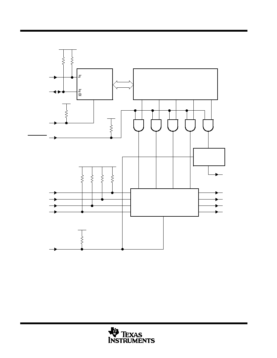
logic diagram (positive logic)
5-Bit Nonvolatile Register
I2C
Interface
Logic
Address:
1001110
1-Bit
Transparent
Latch
4-Bit 1-of-2 Multiplexer
NON-MUXED
OUT
MUX OUT A
MUX OUT B
MUX OUT C
MUX OUT D
MUX IN A
SCL
SDA
OVERRIDE
WP
MUX IN B
MUX IN C
MUX IN D
MUX SELECT
VCC
VCC
VCC
VCC
VCC
1
2
15
3
4
5
6
7
13
14
12
11
10
9
PCA8550
NONVOLATILE 5-BIT REGISTER
WITH I
2
C INTERFACE
SCPS050A ≠ MARCH 1999 ≠ REVISED APRIL 1999
3
POST OFFICE BOX 655303
∑
DALLAS, TEXAS 75265
I
2
C interface
I
2
C communication with this device is initiated by a master sending a start condition, a high-to-low transition on
the serial data (SDA) input/output while the serial clock (SCL) input is high. After the start condition, the device
address byte is sent, MSB first, including the data-direction bit (R/W). This device does not respond to the
general call address. After receiving the valid address byte, this device responds with an acknowledge, a low
on the SDA input/output during the high of the acknowledge-related clock pulse.
The data byte follows the address acknowledge. If the R/W bit is high, the data from this device are the values
read from the nonvolatile register. If the R/W bit is low, the data are from the master, to be written into the register.
A valid data byte is one in which the three high-order bits are low. The first valid data byte that is received is
written into the register, following the stop condition. If an invalid data byte is received, it is acknowledged, but
is not written into the register. The data byte is followed by an acknowledge sent from this device. If other data
bytes are sent from the master following the acknowledge, they are ignored by this device.
A stop condition, a low-to-high transition on the SDA input/output while the SCL input is high, is sent by the
master. If the WP input is low during the falling edge of the first valid data byte acknowledge on the SCL input
and the R/W bit is low, the stop condition causes the I
2
C interface logic to write the data byte value into the
nonvolatile register. Data are written only if complete bytes are received and acknowledged. Writing to the
register takes time (t
wr
), during which the device does not respond to its slave address. If the WP input is high,
the I
2
C interface logic does not write to the register.
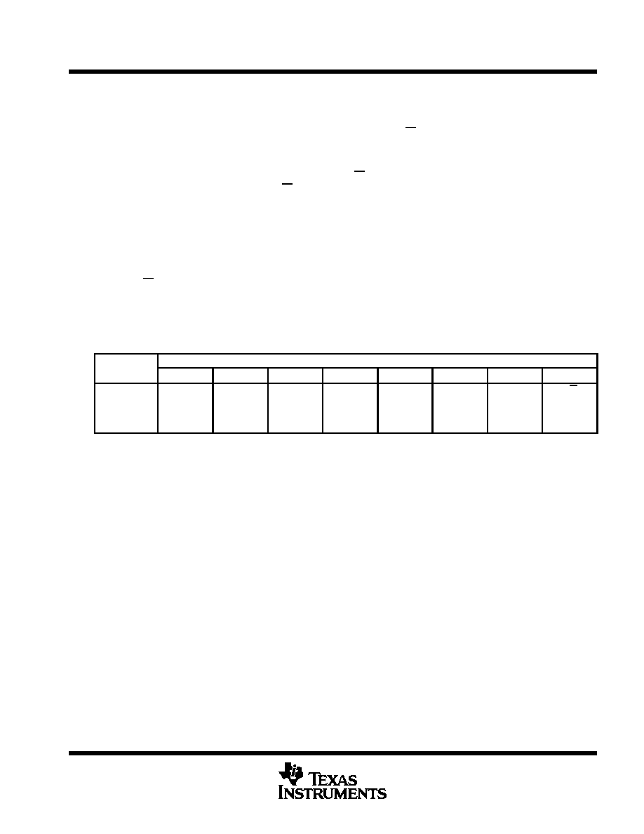
I2C INTERFACE DEFINITION TABLE
BYTE
BIT
BYTE
7 (MSB)
6
5
4
3
2
1
0 (LSB)
Address
H
L
L
H
H
H
L
R/W
Data
L
L
L
NON-
MUXED
OUT
MUX OUT
D
MUX OUT
C
MUX OUT
B
MUX OUT
A
absolute maximum ratings over operating free-air temperature range (unless otherwise noted)
Supply voltage range, V
CC
≠0.5 V to 6.5 V
. . . . . . . . . . . . . . . . . . . . . . . . . . . . . . . . . . . . . . . . . . . . . . . . . . . . . . . . .
Input voltage range, V
I
(see Note 1)
≠0.5 V to 6.5 V
. . . . . . . . . . . . . . . . . . . . . . . . . . . . . . . . . . . . . . . . . . . . . . . . .
Output voltage range, V
O
(SDA) (see Note 1)
≠0.5 V to 6.5 V
. . . . . . . . . . . . . . . . . . . . . . . . . . . . . . . . . . . . . . . .
Output voltage range, V
O
(MUX OUT outputs) (see Note 1)
≠0.5 V to 2.9 V
. . . . . . . . . . . . . . . . . . . . . . . . . . . .
Output voltage range, V
O
(NON-MUXED OUT output) (see Notes 1 and 2)
≠0.5 V to V
CC
+ 0.5 V
. . . . . . . . .
Input clamp current, I
IK
(V
I
< 0 )
≠50 mA
. . . . . . . . . . . . . . . . . . . . . . . . . . . . . . . . . . . . . . . . . . . . . . . . . . . . . . . . . .
Output clamp current, I
OK
(V
O
< 0 or V
O
> V
CC
) (see Note 2)
≠50 mA, +10 mA
. . . . . . . . . . . . . . . . . . . . . . . .
Input/output clamp current, I
OK
(V
O
< 0)
≠50 mA
. . . . . . . . . . . . . . . . . . . . . . . . . . . . . . . . . . . . . . . . . . . . . . . . . . .
Continuous output current, I
O
(V
O
= 0 to V
CC
) (see Note 2)
±
15 mA
. . . . . . . . . . . . . . . . . . . . . . . . . . . . . . . . . .
Continuous current through V
CC
or GND
±
30 mA
. . . . . . . . . . . . . . . . . . . . . . . . . . . . . . . . . . . . . . . . . . . . . . . . . . .
Package thermal impedance,
JA
(see Note 3): D package
113
∞
C/W
. . . . . . . . . . . . . . . . . . . . . . . . . . . . . . . . . .
DB package
131
∞
C/W
. . . . . . . . . . . . . . . . . . . . . . . . . . . . . . . .
PW package
149
∞
C/W
. . . . . . . . . . . . . . . . . . . . . . . . . . . . . . . .
Storage temperature range, T
stg
≠65
∞
C to 85
∞
C
. . . . . . . . . . . . . . . . . . . . . . . . . . . . . . . . . . . . . . . . . . . . . . . . . . . .
Stresses beyond those listed under "absolute maximum ratings" may cause permanent damage to the device. These are stress ratings only, and
functional operation of the device at these or any other conditions beyond those indicated under "recommended operating conditions" is not
implied. Exposure to absolute-maximum-rated conditions for extended periods may affect device reliability.
NOTES:
1. The input negative-voltage and output voltage ratings may be exceeded if the input and output current ratings are observed.
2. The value of VCC is provided in the recommended operating conditions table.
3. The package thermal impedance is calculated in accordance with JESD 51.

PCA8550
NONVOLATILE 5-BIT REGISTER
WITH I
2
C INTERFACE
SCPS050A ≠ MARCH 1999 ≠ REVISED APRIL 1999
4
POST OFFICE BOX 655303
∑
DALLAS, TEXAS 75265
recommended operating conditions
MIN
MAX
UNIT
VCC
Supply voltage
3
3.6
V
SCL, SDA
2.7
4
VIH
High-level input voltage
OVERRIDE, MUX IN,
MUX SELECT, WP
2
4
V
SCL, SDA
≠0.5
0.9
VIL
Low-level input voltage
OVERRIDE, MUX IN,
MUX SELECT, WP
≠0.5
0.8
V
IOH
High-level output current
MUX OUT,
NON-MUXED OUT
≠2
mA
SDA
6
IOL
Low-level output current
MUX OUT,
NON-MUXED OUT
2
mA
t/
v
Input transition rise or fall rate
OVERRIDE, MUX IN,
MUX SELECT, WP
10
ns/V
TA
Operating free-air temperature
0
70
∞
C
electrical characteristics over recommended operating free-air temperature range,
V
CC
= 3.3 V
±
0.3 V (unless otherwise noted)
PARAMETER
TEST CONDITIONS
MIN
MAX
UNIT
VIK
Input diode clamp voltage
II = ≠18 mA
≠1.5
V
Vhys
SCL, SDA
0.19
V
MUX OUT
IOH = ≠100
µ
A
2
2.625
VOH
MUX OUT
IOH = ≠1 mA
1.7
2.625
V
VOH
NON MUXED OUT
IOH = ≠100
µ
A
2.4
3.6
V
NON-MUXED OUT
IOH = ≠2 mA
2
3.6
MUX OUT
IOL = 100
µ
A
≠0.3
0.4
MUX OUT
IOL = 2 mA
≠0.3
0.7
VOL
NON MUXED OUT
IOL = 100
µ
A
≠0.5
0.4
V
VOL
NON-MUXED OUT
IOL = 2 mA
≠0.5
0.7
V
SDA
IOL = 3 mA
0.4
SDA
IOL = 6 mA
0.6
SCL, SDA
≠1.5
≠12
µ
A
IIH
OVERRIDE, MUX SELECT, WP
VIH = 2.4 V
≠20
≠100
µ
A
MUX IN
≠0.166
≠0.75
mA
SCL, SDA
≠7
≠32
µ
A
IIL
OVERRIDE, MUX SELECT, WP
VIL = 0.4 V
≠86
≠267
µ
A
MUX IN
≠0.72
≠2
mA
ICC
During read or write cycle
VI = 0 to VCC,
IO = 0,
VCC = 3.3 V
10
mA
ICC
Not during read or write cycle
VI = VCC,
IO = 0
500
µ
A
Ci
VI = VCC or GND
10
pF
Vhys is the hysteresis of Schmitt-trigger inputs.

PCA8550
NONVOLATILE 5-BIT REGISTER
WITH I
2
C INTERFACE
SCPS050A ≠ MARCH 1999 ≠ REVISED APRIL 1999
5
POST OFFICE BOX 655303
∑
DALLAS, TEXAS 75265
nonvolatile storage specifications
PARAMETER
SPECIFICATIONS
Write time (twr)
10 ms, typical
Memory-cell data retention
10 years, minimum
Maximum number of memory-cell write cycles
1000 cycles, minimum
I
2
C interface timing requirements over recommended operating free-air temperature range (unless
otherwise noted) (see Figure 1)
VCC = 3.3 V
±
0.3 V
UNIT
MIN
MAX
UNIT
fscl
I2C clock frequency
10
400
kHz
Tsch
I2C clock high time
600
ns
Tscl
I2C clock low time
1.3
µ
s
Tsp
I2C spike time
0
50
ns
Tsds
I2C serial data setup time
100
ns
Tsdh
I2C serial data hold time
0
900
ns
Ticr
I2C input rise time
20
300
ns
Ticf
I2C input fall time
20
300
ns
Tocf
I2C output fall time (10-pF to 400-pF bus)
20 + 0.1 Cb
250
ns
Tbuf
I2C bus free time between stop and start
1.3
µ
s
Tsts
I2C start or repeated start condition setup
600
ns
Tsth
I2C start or repeated start condition hold
600
ns
Tsps
I2C stop condition setup
600
ns
Cb
I2C bus capacitive load
400
pF
Cb = capacitance of one bus line in pF.
switching characteristics over recommended operating free-air temperature range (unless
otherwise noted) (see Figure 2)
PARAMETER
FROM
(INPUT)
TO
(OUTPUT)
VCC = 3.3 V
±
0.3 V
UNIT
(INPUT)
(OUTPUT)
MIN
MAX
tmpd
Mux input to output
propagation delay
MUX IN
MUX OUT
20
ns
tsov
MUX SELECT to output valid
MUX SELECT
Output valid
22
ns
tovn
OVERRIDE to NON-MUXED
OUT output delay
OVERRIDE
NON-MUXED OUT
15
ns
tovm
OVERRIDE to MUX OUT
output delay
OVERRIDE
MUX OUT
25
ns
tsu
Setup time
WP
Falling edge of first valid data byte
acknowledge on the SCL input
30
ns
th
Hold time
WP
Falling edge of first valid data byte
acknowledge on the SCL input
120
ns
tr
Output rise time
1
3
ns/V
tf
Output fall time
1
3
ns/V