www.ti.com
FEATURES
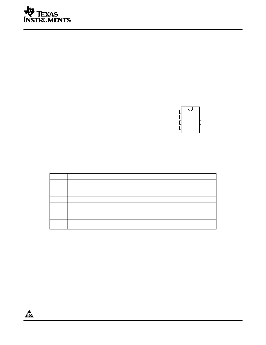
DCT OR DCU PACKAGE
(TOP VIEW)
1
2
3
4
8
7
6
5
GND
V
REF1
SCL1
SDA1
EN
V
REF2
SCL2
SDA2
PCA9306
DUAL BIDIRECTIONAL I2C BUS AND SMBus VOLTAGE-LEVEL TRANSLATOR
SCPS113 ≠ OCTOBER 2004 ≠ REVISED APRIL 2005
∑
Lock-Up-Free Operation for Isolation When
EN = Low
∑
2-Bit Bidirectional Translator for SDA and SCL
Lines in Mixed-Mode I
2
C Applications
∑
Flow-Through Pinout for Ease of Printed
Circuit Board Trace Routing
∑
I
2
C and SMBus Compatible
∑
Latch-Up Performance Exceeds 100 mA Per
∑
Less Than 1.5-ns Maximum Propagation Delay
JESD 78, Class II
to Accommodate Standard-Mode and
Fast-Mode I
2
C Devices and Multiple Masters
∑
ESD Protection Exceeds JESD 22
∑
Allows Voltage-Level Translator Between
≠ 2000-V Human-Body Model (A114-A)
≠ 1.2-V V
REF1
and 2.5-V, 3.3-V, or 5-V V
REF2
≠ 200-V Machine Model (A115-A)
≠ 1.8-V V
REF1
and 3.3-V or 5-V V
REF2
≠ 1000-V Charged-Device Model (C101)
≠ 2.5-V V
REF1
and 5-V V
REF2
≠ 3.3-V V
REF1
and 5-V V
REF2
∑
Provides Bidirectional Voltage Translation
With No Direction Pin
∑
Low 3.5-
ON-State Connection Between
Input and Output Ports Provides Less Signal
Distortion
∑
Open-Drain I
2
C I/O Ports (SCL1, SDA1, SCL2,
and SDA2)
∑
5-V Tolerant I
2
C I/O Ports to Support
Mixed-Mode Signal Operation
∑
High-Impedance SCL1, SDA1, SCL2, and
SDA2 Pins for EN = Low
PIN
SYMBOL
FUNCTION
1
GND
Ground, 0 V
2
V
REF1
Low-voltage-side reference supply voltage for SCL1 and SDA1
3
SCL1
Serial clock, low-voltage side. Connect to V
REF1
through a pullup resistor.
4
SDA1
Serial data, low-voltage side. Connect to V
REF1
through a pullup resistor.
5
SDA2
Serial data, high-voltage side. Connect to V
REF2
through a pullup resistor.
6
SCL2
Serial clock, high-voltage side. Connect to V
REF2
through a pullup resistor.
7
V
REF2
High-voltage-side reference supply voltage for SCL2 and SDA2
Switch enable input. Connected to V
REF2
and pulled up through a high
8
EN
resistor.
Please be aware that an important notice concerning availability, standard warranty, and use in critical applications of Texas
Instruments semiconductor products and disclaimers thereto appears at the end of this data sheet.
PRODUCTION DATA information is current as of publication date.
Copyright © 2004≠2005, Texas Instruments Incorporated
Products conform to specifications per the terms of the Texas
Instruments standard warranty. Production processing does not
necessarily include testing of all parameters.
www.ti.com
DESCRIPTION/ORDERING INFORMATION
PCA9306
DUAL BIDIRECTIONAL I2C BUS AND SMBus VOLTAGE-LEVEL TRANSLATOR
SCPS113 ≠ OCTOBER 2004 ≠ REVISED APRIL 2005
This dual bidirectional I
2
C and SMBus voltage-level translator, with an enable (EN) input, is operational from
1.2-V to 3.3-V V
REF1
and 2.5-V to 5.5-V V
REF2
.
The PCA9306 allows bidirectional voltage translations between 1.2 V and 5 V, without the use of a direction pin.
The low ON-state resistance (r
on
) of the switch allows connections to be made with minimal propagation delay.
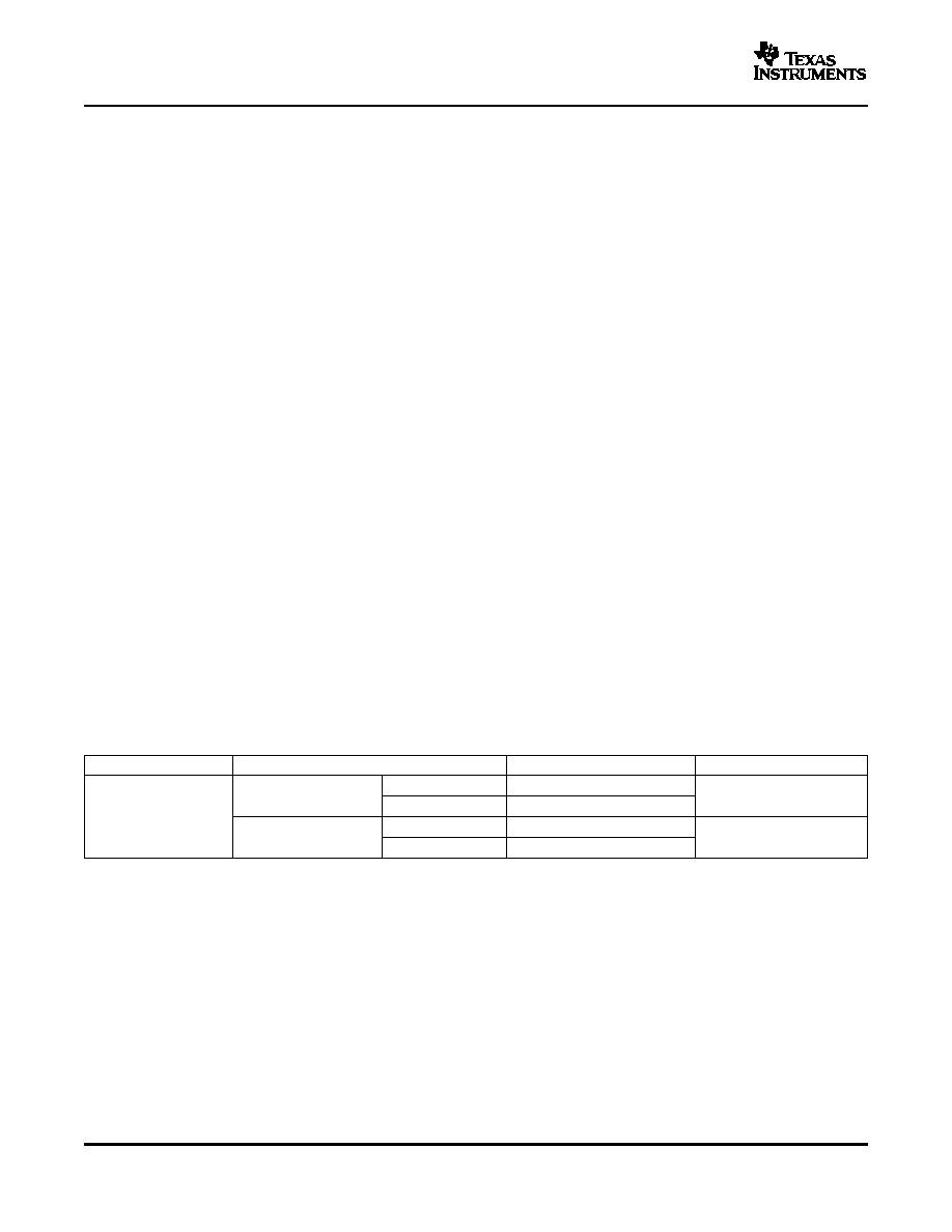
When EN is high, the translator switch is ON, and the SCL1 and SDA1 I/O are connected to the SCL2 and SDA2
I/O, respectively, allowing bidirectional data flow between ports. When EN is low, the translator switch is off, and
a high-impedance state exists between ports.
In I
2
C applications, the bus capacitance limit of 400 pF restricts the number of devices and bus length. Using the
PCA9306 enables the system designer to isolate two halves of a bus; thus, more I
2
C devices or longer trace
length can be accommodated.
The PCA9306 also can be used to run two buses, one at 400-kHz operating frequency and the other at 100-kHz
operating frequency. If the two buses are operating at different frequencies, the 100-kHz bus must be isolated
when the 400-kHz operation of the other bus is required. If the master is running at 400 kHz, the maximum
system operating frequency may be less than 400 kHz because of the delays added by the repeater.
As with the standard I
2
C system, pullup resistors are required to provide the logic high levels on the translator's
bus. The PCA9306 has a standard open-collector configuration of the I
2
C bus. The size of these pullup resistors
depends on the system, but each side of the repeater must have a pullup resistor. The device is designed to
work with standard-mode and fast-mode I
2
C devices, in addition to SMBus devices. Standard-mode I
2
C devices
only specify 3 mA in a generic I
2
C system where standard-mode devices and multiple masters are possible.
Under certain conditions, high termination currents can be used.
When the SDA1 or SDA2 port is low, the clamp is in the ON state, and a low resistance connection exists
between the SDA1 and SDA2 ports. Assuming the higher voltage is on the SDA2 port when the SDA2 port is
high, the voltage on the SDA1 port is limited to the voltage set by V
REF1
. When the SDA1 port is high, the SDA2
port is pulled to the drain pullup supply voltage (V
DPU
) by the pullup resistors. This functionality allows a
seamless translation between higher and lower voltages selected by the user, without the need for directional
control. The SCL1/SCL2 channel also functions as the SDA1/SDA2 channel.
All channels have the same electrical characteristics, and there is minimal deviation from one output to another in
voltage or propagation delay. This is a benefit over discrete transistor voltage translation solutions, since the
fabrication of the switch is symmetrical. The translator provides excellent ESD protection to lower-voltage devices
and at the same time protects less ESD-resistant devices.
ORDERING INFORMATION
T
A
PACKAGE
(1)
ORDERABLE PART NUMBER
TOP-SIDE MARKING
(2)
Reel of 3000
PCA9306DCTR
SSOP ≠ DCT
7BD_ _ _
Reel of 250
PCA9306DCTT
≠40∞C to 85∞C
Reel of 3000
PCA9306DCUR
VSSOP ≠ DCU
7BD_
Reel of 250
PCA9306DCUT
(1)
Package drawings, standard packing quantities, thermal data, symbolization, and PCB design guidelines are available at
www.ti.com/sc/package.
(2)
DCT: The actual top-side marking has three additional characters that designate the year, month, and assembly/test site.
DCU: The actual top-side marking has one additional character that designates the assembly/test site.
2

www.ti.com
SCL2
SDA2
SCL1
SDA1
V
REF1
GND
V
REF2
8
7
6
5
1
2
3
4
SW
SW
EN
PCA9306
DUAL BIDIRECTIONAL I2C BUS AND SMBus VOLTAGE-LEVEL TRANSLATOR
SCPS113 ≠ OCTOBER 2004 ≠ REVISED APRIL 2005
FUNCTION TABLE
INPUT
TRANSLATOR FUNCTION
EN
(1)
H
SCL1 = SCL2, SDA1 = SDA2
L
Disconnect
(1)
EN is controlled by the V
REF2
logic levels and should be at least 1 V higher than V
REF1
for best
translator operation.
LOGIC DIAGRAM (POSITIVE LOGIC)
3
www.ti.com
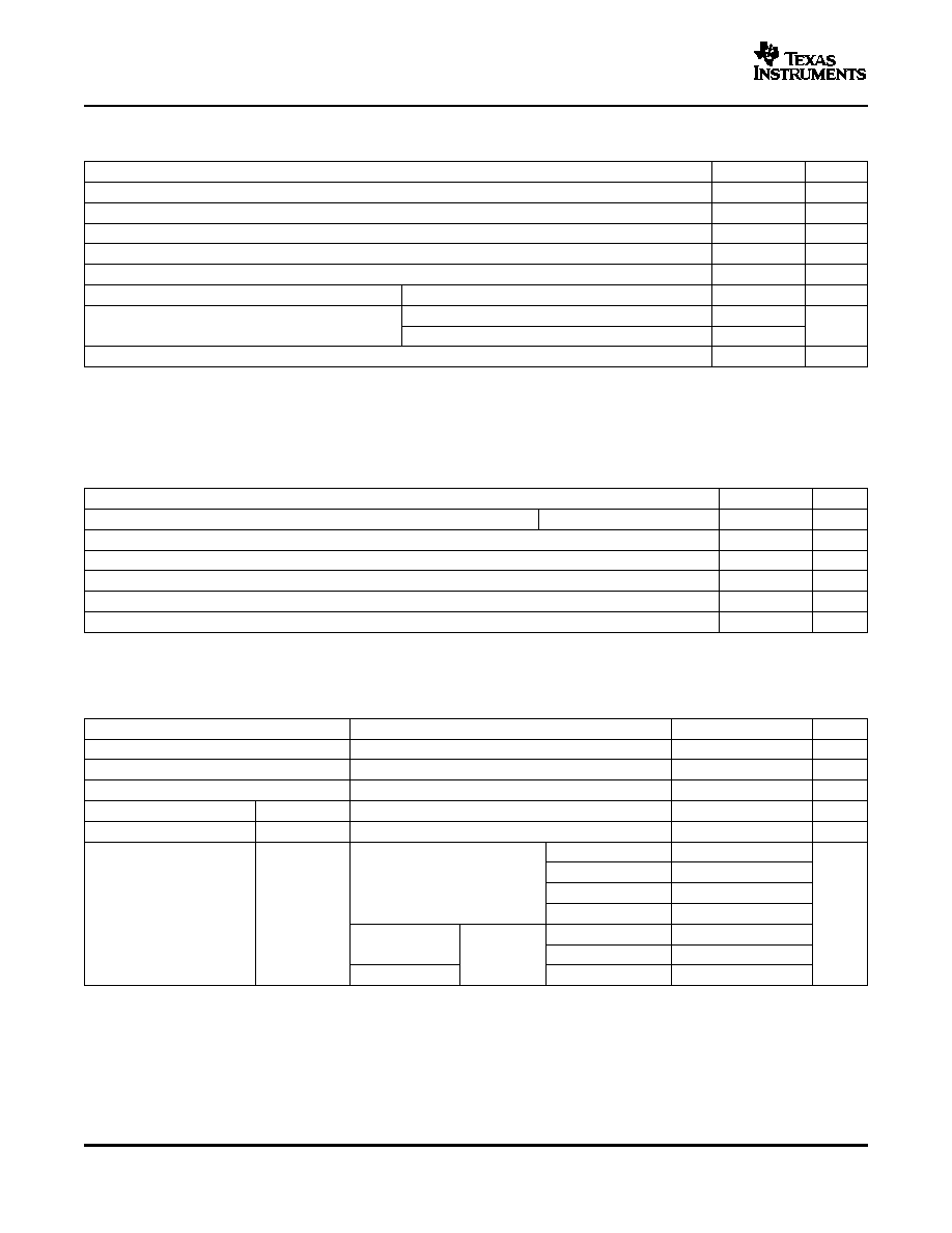
Absolute Maximum Ratings
(1)
Recommended Operating Conditions
Electrical Characteristics
PCA9306
DUAL BIDIRECTIONAL I2C BUS AND SMBus VOLTAGE-LEVEL TRANSLATOR
SCPS113 ≠ OCTOBER 2004 ≠ REVISED APRIL 2005
over operating free-air temperature range (unless otherwise noted)
MIN
MAX
UNIT
V
REF1
DC reference voltage range
≠0.5
7
V
V
REF2
DC reference bias voltage range
≠0.5
7
V
V
I
Input voltage range
(2)
≠0.5
7
V
V
I/O
Input/output voltage range
(2)
≠0.5
7
V
Continuous channel current
128
mA
I
IK
Input clamp current
V
I
< 0
≠50
mA
DCT package
220
JA
Package thermal impedance
(3)
∞C/W
DCU package
227
T
stg
Storage temperature range
≠65
150
∞C
(1)
Stresses beyond those listed under "absolute maximum ratings" may cause permanent damage to the device. These are stress ratings
only, and functional operation of the device at these or any other conditions beyond those indicated under "recommended operating
conditions" is not implied. Exposure to absolute-maximum-rated conditions for extended periods may affect device reliability.
(2)
The input and input/output negative voltage ratings may be exceeded if the input and output current ratings are observed.
(3)
The package thermal impedance is calculated in accordance with JESD 51-7.
MIN
MAX
UNIT
V
I/O
Input/output voltage
SCL1, SDA1, SCL2, SDA2
0
5
V
V
REF1
(1)
Reference voltage
0
5
V
V
REF2
(1)
Reference voltage
0
5
V
EN
Enable input voltage
0
5
V
I
PASS
Pass switch current
64
mA
T
A
Operating free-air temperature
≠40
85
∞
C
(1)
V
REF1
V
REF2
≠ 1 V for best results in level-shifting applications
over recommended operating free-air temperature range (unless otherwise noted)
PARAMETER
TEST CONDITIONS
MIN TYP
(1)
MAX
UNIT
V
IK
Input clamp voltage
I
I
= ≠18 mA,
EN = 0 V
≠1.2
V
I
IH
Input leakage current
V
I
= 5 V,
EN = 0 V
5
µA
C
i
(EN)
Input capacitance
V
I
= 3 V or 0
11
pF
C
io(off)
Off capacitance
SCLn, SDAn
V
O
= 3 V or 0,
EN = 0 V
4
6
pF
C
io(on)
On capacitance
SCLn, SDAn
V
O
= 3 V or 0,
EN = 3 V
10.5
12.5
pF
EN = 4.5 V
3.5
5.5
EN = 3 V
4.7
7
V
I
= 0,
I
O
= 64 mA
EN = 2.3 V
6.3
9.5
r
on
(2)
On resistance
SCLn, SDAn
EN = 1.5 V
25.5
32
EN = 4.5 V
4.8
7.5
V
I
= 2.4 V
I
O
= 15 mA
EN = 3 V
14.7
23
V
I
= 1.7 V
EN = 2.3 V
11.3
16.5
(1)
All typical values are at T
A
= 25∞C.
(2)
Measured by the voltage drop between the SCL1 and SCL2, or SDA1 and SDA2 terminals, at the indicated current through the switch.
On-state resistance is determined by the lowest voltage of the two terminals.
4

www.ti.com
AC PERFORMANCE (TRANSLATING DOWN)
Switching Characteristics
Switching Characteristics
AC PERFORMANCE (TRANSLATING UP)
Switching Characteristics
Switching Characteristics
PCA9306
DUAL BIDIRECTIONAL I2C BUS AND SMBus VOLTAGE-LEVEL TRANSLATOR
SCPS113 ≠ OCTOBER 2004 ≠ REVISED APRIL 2005
over recommended operating free-air temperature range, EN = 3.3 V, V
IH
= 3.3 V, V
IL
= 0, and V
M
= 1.15 V (unless otherwise
noted) (see
Figure 1
)
C
L
= 50 pF
C
L
= 30 pF
C
L
= 15 pF
FROM
TO
PARAMETER
UNIT
(INPUT)
(OUTPUT)
MIN
MAX
MIN
MAX
MIN
MAX
t
PLH
0
0.8
0
0.6
0
0.3
SCL2 or SDA2
SCL1 or SDA1
ns
t
PHL
0
1.2
0
1
0
0.5
over recommended operating free-air temperature range, EN = 2.5 V, V
IH
= 2.5 V, V
IL
= 0, and V
M
= 0.75 V (unless otherwise
noted) (see
Figure 1
)
C
L
= 50 pF
C
L
= 30 pF
C
L
= 15 pF
FROM
TO
PARAMETER
UNIT
(INPUT)
(OUTPUT)
MIN
MAX
MIN
MAX
MIN
MAX
t
PLH
0
1
0
0.7
0
0.4
SCL2 or SDA2
SCL1 or SDA1
ns
t
PHL
0
1.3
0
1
0
0.6
over recommended operating free-air temperature range, EN = 3.3 V, V
IH
= 2.3 V, V
IL
= 0, V
T
= 3.3 V, V
M
= 1.15 V, and
R
L
= 300
(unless otherwise noted) (see
Figure 1
)
C
L
= 50 pF
C
L
= 30 pF
C
L
= 15 pF
FROM
TO
PARAMETER
UNIT
(INPUT)
(OUTPUT)
MIN
MAX
MIN
MAX
MIN
MAX
t
PLH
0
0.9
0
0.6
0
0.4
SCL1 or SDA1
SCL2 or SDA2
ns
t
PHL
0
1.4
0
1.1
0
0.7
over recommended operating free-air temperature range, EN = 2.5 V, V
IH
= 1.5 V, V
IL
= 0, V
T
= 2.5 V, V
M
= 0.75 V, and
R
L
= 300
(unless otherwise noted) (see
Figure 1
)
C
L
= 50 pF
C
L
= 30 pF
C
L
= 15 pF
FROM
TO
PARAMETER
UNIT
(INPUT)
(OUTPUT)
MIN
MAX
MIN
MAX
MIN
MAX
t
PLH
0
1
0
0.6
0
0.4
SCL1 or SDA1
SCL2 or SDA2
ns
t
PHL
0
1.3
0
1.3
0
0.8
5