PCI1031
PCI-TO-PC CARD16 CONTROLLER UNIT
SCPS008B ≠ FEBRUARY 1996 ≠ REVISED DECEMBER 1997
1
POST OFFICE BOX 655303
∑
DALLAS, TEXAS 75265
D
3.3-V Core Logic With Universal PCI
Interface Compatible and 3.3-V or 5-V PCI
Signaling Environments
D
Supports PCI Local Bus Specification 2.1
D
Mix-and-Match 5-V/3.3-V PC Card16 Cards
D
Supports Two PC Card
TM
Slots With Hot
Insertion and Removal
D
1995 PC Card Standard Compliant
D
Low-Power Advanced Submicron CMOS
Technology
D
Uses Serial Interface to Texas Instruments
(TI
TM
) TPS2206 Dual Power Switch
D
System Interrupts Can Be Programmed as
PCI-Style or ISA IRQ-Style Interrupts
D
ISA IRQ Interrupts Can Be Serialized Onto a
Single IRQSER Pin
D
Independent Read and Write Buffers for
Each Direction
D
Multifunction PCI Device With Separate
Configuration Spaces for Each Socket
D
Five PCI Memory Windows and Two I/O
Windows Available to Each PC Card16
Socket
D
Exchangeable Card Architecture
(ExCA)-Compatible Registers Are Mapped
in Memory and I/O Space
D
TI Extension Registers Are Mapped in the
PCI Configuration Space
D
Intel
TM
82365SL-DF Register Compatible
D
Supports 16-Bit Distributed Direct Memory
Access (DMA) on Both PC Card Sockets
D
Supports PC/PCI DMA on Both PC Card
Sockets
D
Supports Zoom Video Mode
D
Supports Ring Indicate
D
Packaged in a 208-Pin Thin Plastic Quad
Flatpack
Description
2
. . . . . . . . . . . . . . . . . . . . . . . . . . . . . . . . . . . . . . . . . . . .
System Block Diagram ≠ 16-Bit PC Card Interface
3
. . . . . . . . . .
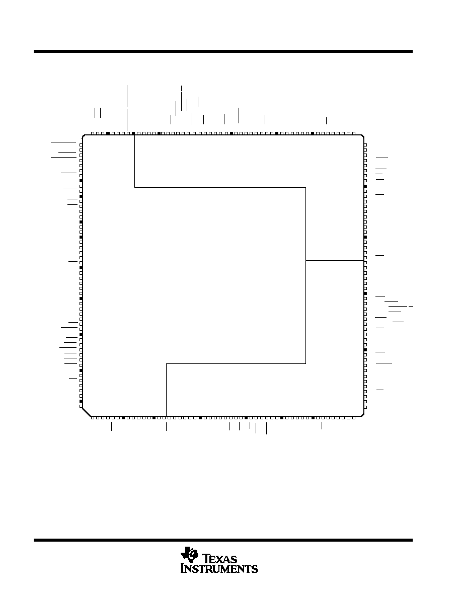
Terminal Assignments ≠ PCI-to-PC Card (16 Bit)
4
. . . . . . . . . . . .
Signal Names/Pin Number Sort Tables
5
. . . . . . . . . . . . . . . . . . . .
Terminal Functions
7
. . . . . . . . . . . . . . . . . . . . . . . . . . . . . . . . . . . . .
Architecture
13
. . . . . . . . . . . . . . . . . . . . . . . . . . . . . . . . . . . . . . . . . .
PC Card DMA and Distributed DMA
28
. . . . . . . . . . . . . . . . . . . . . .
Ring Indicate
31
. . . . . . . . . . . . . . . . . . . . . . . . . . . . . . . . . . . . . . . . .
Zoom Video
32
. . . . . . . . . . . . . . . . . . . . . . . . . . . . . . . . . . . . . . . . . .
Power Management
33
. . . . . . . . . . . . . . . . . . . . . . . . . . . . . . . . . . .
PCI Configuration Header Registers
35
. . . . . . . . . . . . . . . . . . . . .
ExCA Registers
54
. . . . . . . . . . . . . . . . . . . . . . . . . . . . . . . . . . . . . . .
CardBus Socket Registers
75
. . . . . . . . . . . . . . . . . . . . . . . . . . . . . .
DMA Registers
83
. . . . . . . . . . . . . . . . . . . . . . . . . . . . . . . . . . . . . . . .
Absolute Maximum Ratings
89
. . . . . . . . . . . . . . . . . . . . . . . . . . . . . . . .
Recommended Operating Conditions
89
. . . . . . . . . . . . . . . . . . . . . . .
Recommended Operating Conditions for PCI Interface
89
. . . . . . . .
Recommended Operating Conditions for PC Cards A and B
90
. . . .
Electrical Characteristics
91
. . . . . . . . . . . . . . . . . . . . . . . . . . . . . . . . . .
PCI Clock/Reset Timing Requirements
92
. . . . . . . . . . . . . . . . . . . . . .
PCI Timing Requirements
92
. . . . . . . . . . . . . . . . . . . . . . . . . . . . . . . . .
Parameter Measurement Information
93
. . . . . . . . . . . . . . . . . . . . . . . .
PCI Bus Parameter Measurement Information
94
. . . . . . . . . . . . . . . .
PC Card Cycle Timing
95
. . . . . . . . . . . . . . . . . . . . . . . . . . . . . . . . . . . .
Timing Requirements
96
. . . . . . . . . . . . . . . . . . . . . . . . . . . . . . . . . . . . .
Switching Characteristics
97
. . . . . . . . . . . . . . . . . . . . . . . . . . . . . . . . . .
PC Card Parameter Measurement Information
97
. . . . . . . . . . . . . . . .
Mechanical Data
99
. . . . . . . . . . . . . . . . . . . . . . . . . . . . . . . . . . . . . . . . .
Table of Contents
Copyright
©
1997, Texas Instruments Incorporated
Please be aware that an important notice concerning availability, standard warranty, and use in critical applications of
Texas Instruments semiconductor products and disclaimers thereto appears at the end of this data sheet.
Intel and MPIIX are trademarks of Intel Corp.
PC Card is a trademark of Personal Computer Memory Card International Association (PCMCIA).
TI is a trademark of Texas Instruments Incorporated.
PRODUCTION DATA information is current as of publication date.
Products conform to specifications per the terms of Texas Instruments
standard warranty. Production processing does not necessarily include
testing of all parameters.
PCI1031
PCI-TO-PC CARD16 CONTROLLER UNIT
SCPS008B ≠ FEBRUARY 1996 ≠ REVISED DECEMBER 1997
3
POST OFFICE BOX 655303
∑
DALLAS, TEXAS 75265
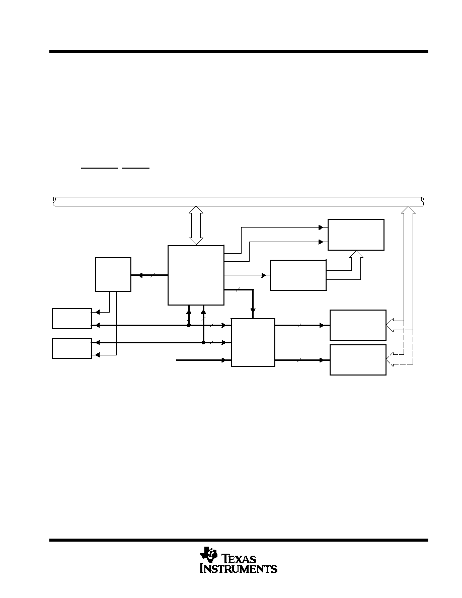
system block diagram ≠ 16-bit PC Card interface
A simplified system block diagram using the PCI1031 is provided below. The PCI950 IRQ deseralizer and the
PCI930 zoomed video (ZV) switch are optional functions that can be used when the system requires that
capability.
The PCI interface includes all address/data and control signals for PCI protocol. The 68-pin PC Card interface
includes all address/data and control signals for 16-bit (R2) protocols. When zoomed video (ZV) is enabled (in
16-bit PC Card mode) 23 of the 68 signals are redefined to support the ZV protocol.
The interrupt interface includes terminals for parallel PCI, parallel ISA, and serialized PCI and ISA signaling.
Other miscellaneous system interface terminals are available on the PCI1031 that include:
D
Multifunction IRQ terminals
D
SUSPEND, RI_OUT (power management control signals)
D
SPKROUT.
PCI Bus
PCI1031
PCI950
IRQSER
Deserializer
IRQSER
3
Interrupt
Controller
INTA
INTB
IRQ2≠15
PCI930
ZV Switch
23
23
PC Card
Socket A
TPS22xx
Power
Switch
3
PC Card
Socket B
External ZV Port
VGA
Controller
Audio
Sub-System
Zoom Video
19
4
Zoom Video
68
68
NOTE: The PC Card interface is 68 pins for CardBus and 16-bit PC Cards. In zoomed-video mode 23 pins are used for routing the zoomed
video signals too the VGA controller.
PCI1031
PCI-TO-PC CARD16 CONTROLLER UNIT
SCPS008B ≠ FEBRUARY 1996 ≠ REVISED DECEMBER 1997
5
POST OFFICE BOX 655303
∑
DALLAS, TEXAS 75265
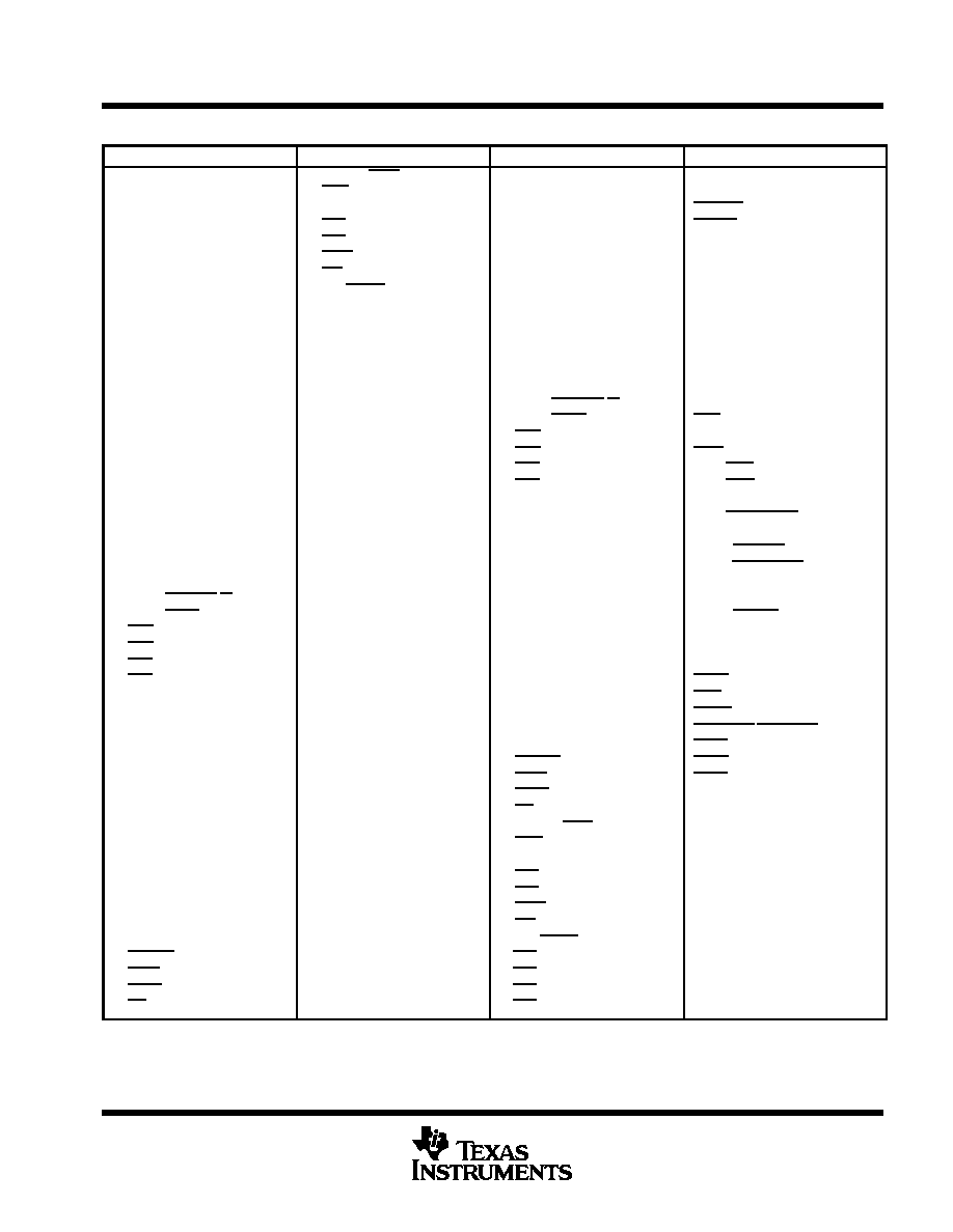
Table 1. Signal Names Sorted Alphabetically ≠ 16-Bit PC Card
SIGNAL NAME
NO.
SIGNAL NAME
NO.
SIGNAL NAME
NO.
SIGNAL NAME
NO.
A_A0
A_A1
A_A2
A_A3
A_A4
A_A5
A_A6
A_A7
A_A8
A_A9
A_A10
A_A11
A_A12
A_A13
A_A14
A_A15
A_A16
A_A17
A_A18
A_A19
A_A20
A_A21
A_A22
A_A23
A_A24
A_A25
A_BVD1(STSCHG/RI)
A_BVD2(SPKR)
A_CD1
A_CD2
A_CE1
A_CE2
A_D0
A_D1
A_D2
A_D3
A_D4
A_D5
A_D6
A_D7
A_D8
A_D9
A_D10
A_D11
A_D12
A_D13
A_D14
A_D15
A_INPACK
A_IORD
A_IOWR
A_OE
133
132
131
128
126
125
123
119
104
102
95
100
117
106
108
115
112
103
105
107
109
111
114
116
118
121
138
137
82
140
94
97
141
144
146
83
85
88
90
92
142
145
147
84
87
89
91
93
127
99
101
98
A_READY(IREQ)
A_REG
A_RESET
A_VS1
A_VS2
A_WAIT
A_WE
A_WP(IOSI16)
AD0
AD1
AD2
AD3
AD4
AD5
AD6
AD7
AD8
AD9
AD10
AD11
AD12
AD13
AD14
AD15
AD16
AD17
AD18
AD19
AD20
AD21
AD22
AD23
AD24
AD25
AD26
AD27
AD28
AD29
AD30
AD31
B_A0
B_A1
B_A2
B_A3
B_A4
B_A5
B_A6
B_A7
B_A8
B_A9
B_A10
B_A11
135
130
124
134
122
136
110
139
15
14
12
11
10
9
8
6
4
3
2
1
208
206
205
204
191
190
189
188
186
185
184
183
179
178
177
176
174
173
171
170
67
66
65
62
60
59
57
54
39
36
29
34
B_A12
B_A13
B_A14
B_A15
B_A16
B_A17
B_A18
B_A19
B_A20
B_A21
B_A22
B_A23
B_A24
B_A25
B_BVD1(STSCHG/RI)
B_BVD2(SPKR)
B_CD1
B_CD2
B_CE1
B_CE2
B_D0
B_D1
B_D2
B_D3
B_D4
B_D5
B_D6
B_D7
B_D8
B_D9
B_D10
B_D11
B_D12
B_D13
B_D14
B_D15
B_INPACK
B_IORD
B_IOWR
B_OE
B_READY(IREQ)
B_REG
B_RESET
B_VS1
B_VS2
B_WAIT
B_WE
B_WP(IOSI16)
C/BE0
C/BE1
C/BE2
C/BE3
52
41
43
50
48
37
40
42
45
47
49
51
53
55
72
71
16
74
28
30
76
78
80
17
19
21
24
26
77
79
81
18
20
23
25
27
61
33
35
32
69
63
58
68
56
70
46
73
5
203
192
180
CLOCK
DATA
DEVSEL
FRAME
GND
GND
GND
GND
GND
GND
GND
GND
GND
GND
GND
GNT
IDSEL
IRDY
IRQ3/INTA
IRQ4/INTB
IRQ5
IRQ7/PCDMAREQ
IRQ9/IRQSER
IRQ10/CLKRUN
IRQ11/PCDMAGNT
IRQ12
IRQ14
IRQ15/RI_OUT
LATCH
PAR
PCLK
PERR
REQ
RSTIN
SPKROUT/SUSPEND
STOP
SERR
TRDY
VCC
VCC
VCC
VCC
VCC
VCC
VCC
VCC
VCC
VCC
VCCA
VCCB
VCCP
VCCP
151
152
197
193
13
22
44
75
96
129
153
167
181
194
207
168
182
195
154
155
156
157
158
159
160
161
162
163
150
202
165
199
169
166
149
198
200
196
7
31
64
86
113
143
164
175
187
201
120
38
148
172