 | –≠–ª–µ–∫—Ç—Ä–æ–Ω–Ω—ã–π –∫–æ–º–ø–æ–Ω–µ–Ω—Ç: PCI7420 | –°–∫–∞—á–∞—Ç—å:  PDF PDF  ZIP ZIP |

PCI7620/PCI7420
Dual Socket CardBus and Smart Card Controller
With Integrated 1394a 2000 OHCI Two Port
PHY/Link Layer Controller and Dedicated
SD/MS Pro Sockets
July 2003
Connectivity Solutions
Data Manual
SCPS077A

iii
Contents
Section
Title
Page
1
Introduction
1≠1
. . . . . . . . . . . . . . . . . . . . . . . . . . . . . . . . . . . . . . . . . . . . . . . . . . . . . .
1.1
Description
1≠1
. . . . . . . . . . . . . . . . . . . . . . . . . . . . . . . . . . . . . . . . . . . . . . . . .
1.2
Features
1≠2
. . . . . . . . . . . . . . . . . . . . . . . . . . . . . . . . . . . . . . . . . . . . . . . . . . .
1.3
Related Documents
1≠3
. . . . . . . . . . . . . . . . . . . . . . . . . . . . . . . . . . . . . . . . . .
1.4
Trademarks
1≠4
. . . . . . . . . . . . . . . . . . . . . . . . . . . . . . . . . . . . . . . . . . . . . . . . .
1.5
Terms and Definitions
1≠5
. . . . . . . . . . . . . . . . . . . . . . . . . . . . . . . . . . . . . . . .
1.6
Ordering Information
1≠5
. . . . . . . . . . . . . . . . . . . . . . . . . . . . . . . . . . . . . . . . .
2
Terminal Descriptions
2≠1
. . . . . . . . . . . . . . . . . . . . . . . . . . . . . . . . . . . . . . . . . . . . .
3
Feature/Protocol Descriptions
3≠1
. . . . . . . . . . . . . . . . . . . . . . . . . . . . . . . . . . . . .
3.1
Power Supply Sequencing
3≠2
. . . . . . . . . . . . . . . . . . . . . . . . . . . . . . . . . . . .
3.2
I/O Characteristics
3≠2
. . . . . . . . . . . . . . . . . . . . . . . . . . . . . . . . . . . . . . . . . . .
3.3
Clamping Voltages
3≠2
. . . . . . . . . . . . . . . . . . . . . . . . . . . . . . . . . . . . . . . . . . .
3.4
Peripheral Component Interconnect (PCI) Interface
3≠2
. . . . . . . . . . . . . .
3.4.1
1394 PCI Bus Master
3≠3
. . . . . . . . . . . . . . . . . . . . . . . . . . . . . . .
3.4.2
Device Resets
3≠3
. . . . . . . . . . . . . . . . . . . . . . . . . . . . . . . . . . . . . .
3.4.3
PCI Bus Lock (LOCK)
3≠3
. . . . . . . . . . . . . . . . . . . . . . . . . . . . . . .
3.4.4
Serial EEPROM I
2
C Bus
3≠3
. . . . . . . . . . . . . . . . . . . . . . . . . . . . .
3.4.5
Functions 0 and 1 (CardBus) Subsystem Identification
3≠4
. . .
3.4.6
Function 2 (OHCI 1394) Subsystem Identification
3≠5
. . . . . . .
3.4.7
Function 3 (Flash Media) Subsystem Identification
3≠5
. . . . . .
3.5
Summary of UltraMedia
t
Cards
3≠5
. . . . . . . . . . . . . . . . . . . . . . . . . . . . . . .
3.5.1
MultiMediaCard (MMC)
3≠5
. . . . . . . . . . . . . . . . . . . . . . . . . . . . . .
3.5.2
Secure Digital (SD)
3≠6
. . . . . . . . . . . . . . . . . . . . . . . . . . . . . . . . .
3.5.3
Memory Stick/MS-Pro
3≠6
. . . . . . . . . . . . . . . . . . . . . . . . . . . . . . .
3.5.4
Smart Card
3≠6
. . . . . . . . . . . . . . . . . . . . . . . . . . . . . . . . . . . . . . . .
3.6
PC Card Applications
3≠6
. . . . . . . . . . . . . . . . . . . . . . . . . . . . . . . . . . . . . . . .
3.6.1
PC Card Insertion/Removal and Recognition
3≠7
. . . . . . . . . . .
3.6.2
Low Voltage CardBus Card Detection
3≠7
. . . . . . . . . . . . . . . . .
3.6.3
UltraMedia Card Detection
3≠7
. . . . . . . . . . . . . . . . . . . . . . . . . . .
3.6.4
Flash Media Card Detection
3≠8
. . . . . . . . . . . . . . . . . . . . . . . . . .
3.6.5
Power Switch Interface
3≠8
. . . . . . . . . . . . . . . . . . . . . . . . . . . . . .
3.6.6
Internal Ring Oscillator
3≠9
. . . . . . . . . . . . . . . . . . . . . . . . . . . . . .
3.6.7
Integrated Pullup Resistors for PC Card Interface
3≠10
. . . . . . .
3.6.8
SPKROUT and CAUDPWM Usage
3≠10
. . . . . . . . . . . . . . . . . . .
3.6.9
LED Socket Activity Indicators
3≠10
. . . . . . . . . . . . . . . . . . . . . . . .
3.6.10
CardBus Socket Registers
3≠11
. . . . . . . . . . . . . . . . . . . . . . . . . . .
3.6.11
48-MHz Clock Requirements
3≠11
. . . . . . . . . . . . . . . . . . . . . . . . .

iv
3.7
Serial EEPROM Interface
3≠12
. . . . . . . . . . . . . . . . . . . . . . . . . . . . . . . . . . . . .
3.7.1
Serial-Bus Interface Implementation
3≠12
. . . . . . . . . . . . . . . . . . .
3.7.2
Accessing Serial-Bus Devices Through Software
3≠12
. . . . . . .
3.7.3
Serial-Bus Interface Protocol
3≠12
. . . . . . . . . . . . . . . . . . . . . . . . .
3.7.4
Serial-Bus EEPROM Application
3≠14
. . . . . . . . . . . . . . . . . . . . . .
3.8
Programmable Interrupt Subsystem
3≠16
. . . . . . . . . . . . . . . . . . . . . . . . . . . .
3.8.1
PC Card Functional and Card Status Change Interrupts
3≠17
.
3.8.2
Interrupt Masks and Flags
3≠18
. . . . . . . . . . . . . . . . . . . . . . . . . . .
3.8.3
Using Parallel IRQ Interrupts
3≠19
. . . . . . . . . . . . . . . . . . . . . . . . .
3.8.4
Using Parallel PCI Interrupts
3≠19
. . . . . . . . . . . . . . . . . . . . . . . . .
3.8.5
Using Serialized IRQSER Interrupts
3≠20
. . . . . . . . . . . . . . . . . . .
3.8.6
SMI Support in the PCI7x20 Device
3≠20
. . . . . . . . . . . . . . . . . . .
3.9
Power Management Overview
3≠20
. . . . . . . . . . . . . . . . . . . . . . . . . . . . . . . .
3.9.1
1394 Power Management (Function 2)
3≠21
. . . . . . . . . . . . . . . .
3.9.2
Integrated Low-Dropout Voltage Regulator (LDO-VR)
3≠21
. . . .
3.9.3
CardBus (Functions 0 and 1) Clock Run Protocol
3≠22
. . . . . . .
3.9.4
CardBus PC Card Power Management
3≠22
. . . . . . . . . . . . . . . .
3.9.5
16-Bit PC Card Power Management
3≠22
. . . . . . . . . . . . . . . . . . .
3.9.6
Suspend Mode
3≠23
. . . . . . . . . . . . . . . . . . . . . . . . . . . . . . . . . . . . .
3.9.7
Requirements for Suspend Mode
3≠23
. . . . . . . . . . . . . . . . . . . . .
3.9.8
Ring Indicate
3≠24
. . . . . . . . . . . . . . . . . . . . . . . . . . . . . . . . . . . . . . .
3.9.9
PCI Power Management
3≠24
. . . . . . . . . . . . . . . . . . . . . . . . . . . . .
3.9.9.1
CardBus Power Management
(Functions 0 and 1)
3≠24
. . . . . . . . . . . . . . . . . . . . . .
3.9.9.2
OHCI 1394 (Function 2) Power
Management
3≠25
. . . . . . . . . . . . . . . . . . . . . . . . . . . .
3.9.9.3
Flash Media (Function 3) Power
Management
3≠26
. . . . . . . . . . . . . . . . . . . . . . . . . . . .
3.9.10
CardBus Bridge Power Management
3≠26
. . . . . . . . . . . . . . . . . .
3.9.11
ACPI Support
3≠26
. . . . . . . . . . . . . . . . . . . . . . . . . . . . . . . . . . . . . .
3.9.12
Master List of PME Context Bits and Global Reset-Only
Bits
3≠27
. . . . . . . . . . . . . . . . . . . . . . . . . . . . . . . . . . . . . . . . . . . . . . .
3.10
IEEE 1394 Application Information
3≠29
. . . . . . . . . . . . . . . . . . . . . . . . . . . . .
3.10.1
PHY Port Cable Connection
3≠29
. . . . . . . . . . . . . . . . . . . . . . . . . .
3.10.2
Crystal Selection
3≠30
. . . . . . . . . . . . . . . . . . . . . . . . . . . . . . . . . . .
3.10.3
Bus Reset
3≠31
. . . . . . . . . . . . . . . . . . . . . . . . . . . . . . . . . . . . . . . . .
4
PC Card Controller Programming Model
4≠1
. . . . . . . . . . . . . . . . . . . . . . . . . . . .
4.1
PCI Configuration Register Map (Functions 0 and 1)
4≠1
. . . . . . . . . . . . .
4.2
Vendor ID Register
4≠2
. . . . . . . . . . . . . . . . . . . . . . . . . . . . . . . . . . . . . . . . . .
4.3
Device ID Register Functions 0 and 1
4≠3
. . . . . . . . . . . . . . . . . . . . . . . . . .
4.4
Command Register
4≠4
. . . . . . . . . . . . . . . . . . . . . . . . . . . . . . . . . . . . . . . . . .
4.5
Status Register
4≠5
. . . . . . . . . . . . . . . . . . . . . . . . . . . . . . . . . . . . . . . . . . . . . .
4.6
Revision ID Register
4≠6
. . . . . . . . . . . . . . . . . . . . . . . . . . . . . . . . . . . . . . . . .
4.7
Class Code Register
4≠6
. . . . . . . . . . . . . . . . . . . . . . . . . . . . . . . . . . . . . . . . .
4.8
Cache Line Size Register
4≠6
. . . . . . . . . . . . . . . . . . . . . . . . . . . . . . . . . . . . .

v
4.9
Latency Timer Register
4≠7
. . . . . . . . . . . . . . . . . . . . . . . . . . . . . . . . . . . . . . .
4.10
Header Type Register
4≠7
. . . . . . . . . . . . . . . . . . . . . . . . . . . . . . . . . . . . . . . .
4.11
BIST Register
4≠7
. . . . . . . . . . . . . . . . . . . . . . . . . . . . . . . . . . . . . . . . . . . . . . .
4.12
CardBus Socket Registers/ExCA Base Address Register
4≠8
. . . . . . . . .
4.13
Capability Pointer Register
4≠8
. . . . . . . . . . . . . . . . . . . . . . . . . . . . . . . . . . . .
4.14
Secondary Status Register
4≠9
. . . . . . . . . . . . . . . . . . . . . . . . . . . . . . . . . . .
4.15
PCI Bus Number Register
4≠10
. . . . . . . . . . . . . . . . . . . . . . . . . . . . . . . . . . . .
4.16
CardBus Bus Number Register
4≠10
. . . . . . . . . . . . . . . . . . . . . . . . . . . . . . . .
4.17
Subordinate Bus Number Register
4≠10
. . . . . . . . . . . . . . . . . . . . . . . . . . . . .
4.18
CardBus Latency Timer Register
4≠11
. . . . . . . . . . . . . . . . . . . . . . . . . . . . . .
4.19
CardBus Memory Base Registers 0, 1
4≠11
. . . . . . . . . . . . . . . . . . . . . . . . . .
4.20
CardBus Memory Limit Registers 0, 1
4≠12
. . . . . . . . . . . . . . . . . . . . . . . . . .
4.21
CardBus I/O Base Registers 0, 1
4≠12
. . . . . . . . . . . . . . . . . . . . . . . . . . . . . .
4.22
CardBus I/O Limit Registers 0, 1
4≠13
. . . . . . . . . . . . . . . . . . . . . . . . . . . . . .
4.23
Interrupt Line Register
4≠13
. . . . . . . . . . . . . . . . . . . . . . . . . . . . . . . . . . . . . . .
4.24
Interrupt Pin Register
4≠14
. . . . . . . . . . . . . . . . . . . . . . . . . . . . . . . . . . . . . . . .
4.25
Bridge Control Register
4≠15
. . . . . . . . . . . . . . . . . . . . . . . . . . . . . . . . . . . . . .
4.26
Subsystem Vendor ID Register
4≠16
. . . . . . . . . . . . . . . . . . . . . . . . . . . . . . . .
4.27
Subsystem ID Register
4≠16
. . . . . . . . . . . . . . . . . . . . . . . . . . . . . . . . . . . . . . .
4.28
PC Card 16-Bit I/F Legacy-Mode Base-Address Register
4≠17
. . . . . . . . .
4.29
System Control Register
4≠18
. . . . . . . . . . . . . . . . . . . . . . . . . . . . . . . . . . . . . .
4.30
MC_CD Debounce Register
4≠20
. . . . . . . . . . . . . . . . . . . . . . . . . . . . . . . . . .
4.31
General Control Register
4≠21
. . . . . . . . . . . . . . . . . . . . . . . . . . . . . . . . . . . . .
4.32
General-Purpose Event Status Register
4≠22
. . . . . . . . . . . . . . . . . . . . . . . .
4.33
General-Purpose Event Enable Register
4≠23
. . . . . . . . . . . . . . . . . . . . . . .
4.34
General-Purpose Input Register
4≠23
. . . . . . . . . . . . . . . . . . . . . . . . . . . . . . .
4.35
General-Purpose Output Register
4≠24
. . . . . . . . . . . . . . . . . . . . . . . . . . . . .
4.36
Multifunction Routing Status Register
4≠25
. . . . . . . . . . . . . . . . . . . . . . . . . .
4.37
Retry Status Register
4≠26
. . . . . . . . . . . . . . . . . . . . . . . . . . . . . . . . . . . . . . . .
4.38
Card Control Register
4≠27
. . . . . . . . . . . . . . . . . . . . . . . . . . . . . . . . . . . . . . . .
4.39
Device Control Register
4≠28
. . . . . . . . . . . . . . . . . . . . . . . . . . . . . . . . . . . . . .
4.40
Diagnostic Register
4≠29
. . . . . . . . . . . . . . . . . . . . . . . . . . . . . . . . . . . . . . . . . .
4.41
Capability ID Register
4≠30
. . . . . . . . . . . . . . . . . . . . . . . . . . . . . . . . . . . . . . . .
4.42
Next Item Pointer Register
4≠30
. . . . . . . . . . . . . . . . . . . . . . . . . . . . . . . . . . . .
4.43
Power Management Capabilities Register
4≠31
. . . . . . . . . . . . . . . . . . . . . .
4.44
Power Management Control/Status Register
4≠32
. . . . . . . . . . . . . . . . . . . .
4.45
Power Management Control/Status Bridge Support Extensions
Register
4≠33
. . . . . . . . . . . . . . . . . . . . . . . . . . . . . . . . . . . . . . . . . . . . . . . . . . . .
4.46
Power-Management Data Register
4≠33
. . . . . . . . . . . . . . . . . . . . . . . . . . . .
4.47
Serial Bus Data Register
4≠34
. . . . . . . . . . . . . . . . . . . . . . . . . . . . . . . . . . . . .
4.48
Serial Bus Index Register
4≠34
. . . . . . . . . . . . . . . . . . . . . . . . . . . . . . . . . . . . .
4.49
Serial Bus Slave Address Register
4≠35
. . . . . . . . . . . . . . . . . . . . . . . . . . . . .
4.50
Serial Bus Control/Status Register
4≠36
. . . . . . . . . . . . . . . . . . . . . . . . . . . . .

vi
5
ExCA Compatibility Registers (Functions 0 and 1)
5≠1
. . . . . . . . . . . . . . . . . .
5.1
ExCA Identification and Revision Register
5≠5
. . . . . . . . . . . . . . . . . . . . . .
5.2
ExCA Interface Status Register
5≠6
. . . . . . . . . . . . . . . . . . . . . . . . . . . . . . . .
5.3
ExCA Power Control Register
5≠7
. . . . . . . . . . . . . . . . . . . . . . . . . . . . . . . . .
5.4
ExCA Interrupt and General Control Register
5≠8
. . . . . . . . . . . . . . . . . . .
5.5
ExCA Card Status-Change Register
5≠9
. . . . . . . . . . . . . . . . . . . . . . . . . . .
5.6
ExCA Card Status-Change Interrupt Configuration Register
5≠10
. . . . . . .
5.7
ExCA Address Window Enable Register
5≠11
. . . . . . . . . . . . . . . . . . . . . . . .
5.8
ExCA I/O Window Control Register
5≠12
. . . . . . . . . . . . . . . . . . . . . . . . . . . .
5.9
ExCA I/O Windows 0 and 1 Start-Address Low-Byte Registers
5≠13
. . . .
5.10
ExCA I/O Windows 0 and 1 Start-Address High-Byte Registers
5≠13
. . . .
5.11
ExCA I/O Windows 0 and 1 End-Address Low-Byte Registers
5≠14
. . . . .
5.12
ExCA I/O Windows 0 and 1 End-Address High-Byte Registers
5≠14
. . . .
5.13
ExCA Memory Windows 0≠4 Start-Address Low-Byte Registers
5≠15
. . .
5.14
ExCA Memory Windows 0≠4 Start-Address High-Byte Registers
5≠16
. . .
5.15
ExCA Memory Windows 0≠4 End-Address Low-Byte Registers
5≠17
. . . .
5.16
ExCA Memory Windows 0≠4 End-Address High-Byte Registers
5≠18
. . .
5.17
ExCA Memory Windows 0≠4 Offset-Address Low-Byte Registers
5≠19
. .
5.18
ExCA Memory Windows 0≠4 Offset-Address High-Byte Registers
5≠20
.
5.19
ExCA Card Detect and General Control Register
5≠21
. . . . . . . . . . . . . . . .
5.20
ExCA Global Control Register
5≠22
. . . . . . . . . . . . . . . . . . . . . . . . . . . . . . . . .
5.21
ExCA I/O Windows 0 and 1 Offset-Address Low-Byte Registers
5≠23
. . .
5.22
ExCA I/O Windows 0 and 1 Offset-Address High-Byte Registers
5≠23
. . .
5.23
ExCA Memory Windows 0≠4 Page Registers
5≠24
. . . . . . . . . . . . . . . . . . .
6
CardBus Socket Registers (Functions 0 and 1)
6≠1
. . . . . . . . . . . . . . . . . . . . . .
6.1
Socket Event Register
6≠2
. . . . . . . . . . . . . . . . . . . . . . . . . . . . . . . . . . . . . . .
6.2
Socket Mask Register
6≠3
. . . . . . . . . . . . . . . . . . . . . . . . . . . . . . . . . . . . . . . .
6.3
Socket Present State Register
6≠4
. . . . . . . . . . . . . . . . . . . . . . . . . . . . . . . .
6.4
Socket Force Event Register
6≠5
. . . . . . . . . . . . . . . . . . . . . . . . . . . . . . . . . .
6.5
Socket Control Register
6≠7
. . . . . . . . . . . . . . . . . . . . . . . . . . . . . . . . . . . . . .
6.6
Socket Power Management Register
6≠8
. . . . . . . . . . . . . . . . . . . . . . . . . . .
7
OHCI Controller Programming Model
7≠1
. . . . . . . . . . . . . . . . . . . . . . . . . . . . . . .
7.1
Vendor ID Register
7≠2
. . . . . . . . . . . . . . . . . . . . . . . . . . . . . . . . . . . . . . . . . .
7.2
Device ID Register
7≠2
. . . . . . . . . . . . . . . . . . . . . . . . . . . . . . . . . . . . . . . . . . .
7.3
Command Register
7≠3
. . . . . . . . . . . . . . . . . . . . . . . . . . . . . . . . . . . . . . . . . .
7.4
Status Register
7≠4
. . . . . . . . . . . . . . . . . . . . . . . . . . . . . . . . . . . . . . . . . . . . . .
7.5
Class Code and Revision ID Register
7≠5
. . . . . . . . . . . . . . . . . . . . . . . . . .
7.6
Latency Timer and Class Cache Line Size Register
7≠5
. . . . . . . . . . . . . .
7.7
Header Type and BIST Register
7≠6
. . . . . . . . . . . . . . . . . . . . . . . . . . . . . . .
7.8
OHCI Base Address Register
7≠6
. . . . . . . . . . . . . . . . . . . . . . . . . . . . . . . . .
7.9
TI Extension Base Address Register
7≠7
. . . . . . . . . . . . . . . . . . . . . . . . . . .
7.10
CardBus CIS Base Address Register
7≠8
. . . . . . . . . . . . . . . . . . . . . . . . . . .
7.11
CardBus CIS Pointer Register
7≠8
. . . . . . . . . . . . . . . . . . . . . . . . . . . . . . . . .
7.12
Subsystem Identification Register
7≠9
. . . . . . . . . . . . . . . . . . . . . . . . . . . . .

vii
7.13
Power Management Capabilities Pointer Register
7≠9
. . . . . . . . . . . . . . .
7.14
Interrupt Line Register
7≠10
. . . . . . . . . . . . . . . . . . . . . . . . . . . . . . . . . . . . . . .
7.15
Interrupt Pin Register
7≠10
. . . . . . . . . . . . . . . . . . . . . . . . . . . . . . . . . . . . . . . .
7.16
Minimum Grant and Maximum Latency Register
7≠11
. . . . . . . . . . . . . . . . .
7.17
OHCI Control Register
7≠11
. . . . . . . . . . . . . . . . . . . . . . . . . . . . . . . . . . . . . . .
7.18
Capability ID and Next Item Pointer Registers
7≠12
. . . . . . . . . . . . . . . . . . .
7.19
Power Management Capabilities Register
7≠13
. . . . . . . . . . . . . . . . . . . . . .
7.20
Power Management Control and Status Register
7≠14
. . . . . . . . . . . . . . . .
7.21
Power Management Extension Registers
7≠14
. . . . . . . . . . . . . . . . . . . . . . .
7.22
PCI Miscellaneous Configuration Register
7≠15
. . . . . . . . . . . . . . . . . . . . . .
7.23
Link Enhancement Control Register
7≠16
. . . . . . . . . . . . . . . . . . . . . . . . . . . .
7.24
Subsystem Access Register
7≠17
. . . . . . . . . . . . . . . . . . . . . . . . . . . . . . . . . .
7.25
GPIO Control Register
7≠18
. . . . . . . . . . . . . . . . . . . . . . . . . . . . . . . . . . . . . . .
8
OHCI Registers
8≠1
. . . . . . . . . . . . . . . . . . . . . . . . . . . . . . . . . . . . . . . . . . . . . . . . . . .
8.1
OHCI Version Register
8≠4
. . . . . . . . . . . . . . . . . . . . . . . . . . . . . . . . . . . . . . .
8.2
GUID ROM Register
8≠5
. . . . . . . . . . . . . . . . . . . . . . . . . . . . . . . . . . . . . . . . .
8.3
Asynchronous Transmit Retries Register
8≠6
. . . . . . . . . . . . . . . . . . . . . . .
8.4
CSR Data Register
8≠6
. . . . . . . . . . . . . . . . . . . . . . . . . . . . . . . . . . . . . . . . . .
8.5
CSR Compare Register
8≠7
. . . . . . . . . . . . . . . . . . . . . . . . . . . . . . . . . . . . . .
8.6
CSR Control Register
8≠7
. . . . . . . . . . . . . . . . . . . . . . . . . . . . . . . . . . . . . . . .
8.7
Configuration ROM Header Register
8≠8
. . . . . . . . . . . . . . . . . . . . . . . . . . .
8.8
Bus Identification Register
8≠8
. . . . . . . . . . . . . . . . . . . . . . . . . . . . . . . . . . . .
8.9
Bus Options Register
8≠9
. . . . . . . . . . . . . . . . . . . . . . . . . . . . . . . . . . . . . . . .
8.10
GUID High Register
8≠10
. . . . . . . . . . . . . . . . . . . . . . . . . . . . . . . . . . . . . . . . . .
8.11
GUID Low Register
8≠10
. . . . . . . . . . . . . . . . . . . . . . . . . . . . . . . . . . . . . . . . . .
8.12
Configuration ROM Mapping Register
8≠11
. . . . . . . . . . . . . . . . . . . . . . . . . .
8.13
Posted Write Address Low Register
8≠11
. . . . . . . . . . . . . . . . . . . . . . . . . . . .
8.14
Posted Write Address High Register
8≠12
. . . . . . . . . . . . . . . . . . . . . . . . . . .
8.15
Vendor ID Register
8≠12
. . . . . . . . . . . . . . . . . . . . . . . . . . . . . . . . . . . . . . . . . .
8.16
Host Controller Control Register
8≠13
. . . . . . . . . . . . . . . . . . . . . . . . . . . . . . .
8.17
Self-ID Buffer Pointer Register
8≠14
. . . . . . . . . . . . . . . . . . . . . . . . . . . . . . . .
8.18
Self-ID Count Register
8≠15
. . . . . . . . . . . . . . . . . . . . . . . . . . . . . . . . . . . . . . .
8.19
Isochronous Receive Channel Mask High Register
8≠16
. . . . . . . . . . . . . .
8.20
Isochronous Receive Channel Mask Low Register
8≠17
. . . . . . . . . . . . . . .
8.21
Interrupt Event Register
8≠18
. . . . . . . . . . . . . . . . . . . . . . . . . . . . . . . . . . . . . .
8.22
Interrupt Mask Register
8≠20
. . . . . . . . . . . . . . . . . . . . . . . . . . . . . . . . . . . . . .
8.23
Isochronous Transmit Interrupt Event Register
8≠22
. . . . . . . . . . . . . . . . . .
8.24
Isochronous Transmit Interrupt Mask Register
8≠23
. . . . . . . . . . . . . . . . . . .
8.25
Isochronous Receive Interrupt Event Register
8≠24
. . . . . . . . . . . . . . . . . . .
8.26
Isochronous Receive Interrupt Mask Register
8≠25
. . . . . . . . . . . . . . . . . . .
8.27
Initial Bandwidth Available Register
8≠25
. . . . . . . . . . . . . . . . . . . . . . . . . . . .
8.28
Initial Channels Available High Register
8≠26
. . . . . . . . . . . . . . . . . . . . . . . .
8.29
Initial Channels Available Low Register
8≠26
. . . . . . . . . . . . . . . . . . . . . . . . .
8.30
Fairness Control Register
8≠27
. . . . . . . . . . . . . . . . . . . . . . . . . . . . . . . . . . . .

viii
8.31
Link Control Register
8≠28
. . . . . . . . . . . . . . . . . . . . . . . . . . . . . . . . . . . . . . . . .
8.32
Node Identification Register
8≠29
. . . . . . . . . . . . . . . . . . . . . . . . . . . . . . . . . . .
8.33
PHY Layer Control Register
8≠30
. . . . . . . . . . . . . . . . . . . . . . . . . . . . . . . . . . .
8.34
Isochronous Cycle Timer Register
8≠31
. . . . . . . . . . . . . . . . . . . . . . . . . . . . .
8.35
Asynchronous Request Filter High Register
8≠32
. . . . . . . . . . . . . . . . . . . . .
8.36
Asynchronous Request Filter Low Register
8≠34
. . . . . . . . . . . . . . . . . . . . .
8.37
Physical Request Filter High Register
8≠35
. . . . . . . . . . . . . . . . . . . . . . . . . .
8.38
Physical Request Filter Low Register
8≠37
. . . . . . . . . . . . . . . . . . . . . . . . . .
8.39
Physical Upper Bound Register (Optional Register)
8≠37
. . . . . . . . . . . . . .
8.40
Asynchronous Context Control Register
8≠38
. . . . . . . . . . . . . . . . . . . . . . . .
8.41
Asynchronous Context Command Pointer Register
8≠39
. . . . . . . . . . . . . .
8.42
Isochronous Transmit Context Control Register
8≠40
. . . . . . . . . . . . . . . . . .
8.43
Isochronous Transmit Context Command Pointer Register
8≠41
. . . . . . . .
8.44
Isochronous Receive Context Control Register
8≠41
. . . . . . . . . . . . . . . . . .
8.45
Isochronous Receive Context Command Pointer Register
8≠43
. . . . . . . .
8.46
Isochronous Receive Context Match Register
8≠44
. . . . . . . . . . . . . . . . . . .
9
TI Extension Registers
9≠1
. . . . . . . . . . . . . . . . . . . . . . . . . . . . . . . . . . . . . . . . . . . .
9.1
DV and MPEG2 Timestamp Enhancements
9≠1
. . . . . . . . . . . . . . . . . . . . .
9.2
Isochronous Receive Digital Video Enhancements
9≠2
. . . . . . . . . . . . . . .
9.3
Isochronous Receive Digital Video Enhancements Register
9≠2
. . . . . . .
9.4
Link Enhancement Register
9≠4
. . . . . . . . . . . . . . . . . . . . . . . . . . . . . . . . . . .
9.5
Timestamp Offset Register
9≠5
. . . . . . . . . . . . . . . . . . . . . . . . . . . . . . . . . . .
10 PHY Register Configuration
10≠1
. . . . . . . . . . . . . . . . . . . . . . . . . . . . . . . . . . . . . . .
10.1
Base Registers
10≠1
. . . . . . . . . . . . . . . . . . . . . . . . . . . . . . . . . . . . . . . . . . . . . .
10.2
Port Status Register
10≠4
. . . . . . . . . . . . . . . . . . . . . . . . . . . . . . . . . . . . . . . . .
10.3
Vendor Identification Register
10≠5
. . . . . . . . . . . . . . . . . . . . . . . . . . . . . . . . .
10.4
Vendor-Dependent Register
10≠6
. . . . . . . . . . . . . . . . . . . . . . . . . . . . . . . . . .
10.5
Power-Class Programming
10≠7
. . . . . . . . . . . . . . . . . . . . . . . . . . . . . . . . . . .
11 Flash Media Controller Programming Model
11≠1
. . . . . . . . . . . . . . . . . . . . . . . .
11.1
Vendor ID Register
11≠2
. . . . . . . . . . . . . . . . . . . . . . . . . . . . . . . . . . . . . . . . . .
11.2
Device ID Register
11≠2
. . . . . . . . . . . . . . . . . . . . . . . . . . . . . . . . . . . . . . . . . . .
11.3
Command Register
11≠3
. . . . . . . . . . . . . . . . . . . . . . . . . . . . . . . . . . . . . . . . . .
11.4
Status Register
11≠4
. . . . . . . . . . . . . . . . . . . . . . . . . . . . . . . . . . . . . . . . . . . . . .
11.5
Class Code and Revision ID Register
11≠5
. . . . . . . . . . . . . . . . . . . . . . . . . .
11.6
Latency Timer and Class Cache Line Size Register
11≠5
. . . . . . . . . . . . . .
11.7
Header Type and BIST Register
11≠6
. . . . . . . . . . . . . . . . . . . . . . . . . . . . . . .
11.8
Flash Media Base Address Register
11≠6
. . . . . . . . . . . . . . . . . . . . . . . . . . .
11.9
Subsystem Vendor Identification Register
11≠7
. . . . . . . . . . . . . . . . . . . . . . .
11.10 Subsystem Identification Register
11≠7
. . . . . . . . . . . . . . . . . . . . . . . . . . . . .
11.11 Capabilities Pointer Register
11≠7
. . . . . . . . . . . . . . . . . . . . . . . . . . . . . . . . . .
11.12 Interrupt Line Register
11≠8
. . . . . . . . . . . . . . . . . . . . . . . . . . . . . . . . . . . . . . .
11.13 Interrupt Pin Register
11≠8
. . . . . . . . . . . . . . . . . . . . . . . . . . . . . . . . . . . . . . . .
11.14 Minimum Grant Register
11≠9
. . . . . . . . . . . . . . . . . . . . . . . . . . . . . . . . . . . . .
11.15 Maximum Latency Register
11≠9
. . . . . . . . . . . . . . . . . . . . . . . . . . . . . . . . . . .

ix
11.16 Capability ID and Next Item Pointer Registers
11≠10
. . . . . . . . . . . . . . . . .
11.17 Power Management Capabilities Register
11≠11
. . . . . . . . . . . . . . . . . . . .
11.18 Power Management Control and Status Register
11≠12
. . . . . . . . . . . . . .
11.19 Power Management Bridge Support Extension Register
11≠12
. . . . . . . .
11.20 Power Management Data Register
11≠13
. . . . . . . . . . . . . . . . . . . . . . . . . .
11.21 General Control Register
11≠13
. . . . . . . . . . . . . . . . . . . . . . . . . . . . . . . . . . .
11.22 Subsystem Access Register
11≠14
. . . . . . . . . . . . . . . . . . . . . . . . . . . . . . . .
11.23 Diagnostic Register
11≠15
. . . . . . . . . . . . . . . . . . . . . . . . . . . . . . . . . . . . . . . .
12 Electrical Characteristics
12≠1
. . . . . . . . . . . . . . . . . . . . . . . . . . . . . . . . . . . . . . . . .
12.1
Absolute Maximum Ratings Over Operating Temperature Ranges
12≠1
.
12.2
Recommended Operating Conditions
12≠1
. . . . . . . . . . . . . . . . . . . . . . . . . .
12.3
Electrical Characteristics Over Recommended Operating
Conditions
12≠3
. . . . . . . . . . . . . . . . . . . . . . . . . . . . . . . . . . . . . . . . . . . . . . . . . .
12.4
Electrical Characteristics Over Recommended Ranges of
Operating Conditions
12≠3
. . . . . . . . . . . . . . . . . . . . . . . . . . . . . . . . . . . . . . . .
12.4.1
Device
12≠3
. . . . . . . . . . . . . . . . . . . . . . . . . . . . . . . . . . . . . . . . . . . .
12.4.2
Driver
12≠4
. . . . . . . . . . . . . . . . . . . . . . . . . . . . . . . . . . . . . . . . . . . . .
12.4.3
Receiver
12≠4
. . . . . . . . . . . . . . . . . . . . . . . . . . . . . . . . . . . . . . . . . . .
12.5
PCI Clock/Reset Timing Requirements Over Recommended
Ranges of Supply Voltage and Operating Free-Air Temperature
12≠4
. . .
12.6
Switching Characteristics for PHY Port Interface
12≠5
. . . . . . . . . . . . . . . . .
12.7
Operating, Timing, and Switching Characteristics of XI
12≠5
. . . . . . . . . . .
12.8
PCI Timing Requirements Over Recommended Ranges of
Supply Voltage and Operating Free-Air Temperature
12≠5
. . . . . . . . . . . . .
13 Mechanical Information
13≠1
. . . . . . . . . . . . . . . . . . . . . . . . . . . . . . . . . . . . . . . . . . .

x
List of Illustrations
Figure
Title
Page
2≠1
PCI7420 and PCI7620 GHK-Package Terminal Diagram
2≠1
. . . . . . . . . . . . .
3≠1
PCI7x20 System Block Diagram
3≠1
. . . . . . . . . . . . . . . . . . . . . . . . . . . . . . . . . .
3≠2
3-State Bidirectional Buffer
3≠2
. . . . . . . . . . . . . . . . . . . . . . . . . . . . . . . . . . . . . . .
3≠3
Serial ROM Application
3≠4
. . . . . . . . . . . . . . . . . . . . . . . . . . . . . . . . . . . . . . . . . .
3≠4
SPKROUT Connection to Speaker Driver
3≠10
. . . . . . . . . . . . . . . . . . . . . . . . . .
3≠5
Two Sample LED Circuits
3≠11
. . . . . . . . . . . . . . . . . . . . . . . . . . . . . . . . . . . . . . . .
3≠6
Serial-Bus Start/Stop Conditions and Bit Transfers
3≠13
. . . . . . . . . . . . . . . . . .
3≠7
Serial-Bus Protocol Acknowledge
3≠13
. . . . . . . . . . . . . . . . . . . . . . . . . . . . . . . . .
3≠8
Serial-Bus Protocol--Byte Write
3≠13
. . . . . . . . . . . . . . . . . . . . . . . . . . . . . . . . . .
3≠9
Serial-Bus Protocol--Byte Read
3≠14
. . . . . . . . . . . . . . . . . . . . . . . . . . . . . . . . . .
3≠10
EEPROM Interface Doubleword Data Collection
3≠14
. . . . . . . . . . . . . . . . . . . .
3≠11
IRQ Implementation
3≠19
. . . . . . . . . . . . . . . . . . . . . . . . . . . . . . . . . . . . . . . . . . . . .
3≠12
System Diagram Implementing CardBus Device Class
Power Management
3≠21
. . . . . . . . . . . . . . . . . . . . . . . . . . . . . . . . . . . . . . . . . . . . .
3≠13
Signal Diagram of Suspend Function
3≠23
. . . . . . . . . . . . . . . . . . . . . . . . . . . . . .
3≠14
RI_OUT Functional Diagram
3≠24
. . . . . . . . . . . . . . . . . . . . . . . . . . . . . . . . . . . . .
3≠15
Block Diagram of a Status/Enable Cell
3≠27
. . . . . . . . . . . . . . . . . . . . . . . . . . . . .
3≠16
TP Cable Connections
3≠29
. . . . . . . . . . . . . . . . . . . . . . . . . . . . . . . . . . . . . . . . . .
3≠17
Typical Compliant DC Isolated Outer Shield Termination
3≠29
. . . . . . . . . . . . .
3≠18
Non-DC Isolated Outer Shield Termination
3≠30
. . . . . . . . . . . . . . . . . . . . . . . . .
3≠19
Load Capacitance for the PCI7x20 PHY
3≠31
. . . . . . . . . . . . . . . . . . . . . . . . . . .
3≠20
Recommended Crystal and Capacitor Layout
3≠31
. . . . . . . . . . . . . . . . . . . . . . .
5≠1
ExCA Register Access Through I/O
5≠2
. . . . . . . . . . . . . . . . . . . . . . . . . . . . . . .
5≠2
ExCA Register Access Through Memory
5≠2
. . . . . . . . . . . . . . . . . . . . . . . . . . .
6≠1
Accessing CardBus Socket Registers Through PCI Memory
6≠1
. . . . . . . . . .
12≠1
Test Load Diagram
12≠4
. . . . . . . . . . . . . . . . . . . . . . . . . . . . . . . . . . . . . . . . . . . . . .

xi
List of Tables
Table
Title
Page
1≠1
Terms and Definitions
1≠5
. . . . . . . . . . . . . . . . . . . . . . . . . . . . . . . . . . . . . . . . . . .
2≠1
Signal Names by GHK Terminal Number
2≠2
. . . . . . . . . . . . . . . . . . . . . . . . . . .
2≠2
CardBus PC Card Signal Names Sorted Alphabetically
2≠6
. . . . . . . . . . . . . .
2≠3
16-Bit PC Card Signal Names Sorted Alphabetically
2≠8
. . . . . . . . . . . . . . . . .
2≠4
Power Supply Terminals
2≠10
. . . . . . . . . . . . . . . . . . . . . . . . . . . . . . . . . . . . . . . . .
2≠5
PC Card Power Switch Terminals
2≠10
. . . . . . . . . . . . . . . . . . . . . . . . . . . . . . . . .
2≠6
PCI System Terminals
2≠11
. . . . . . . . . . . . . . . . . . . . . . . . . . . . . . . . . . . . . . . . . . .
2≠7
PCI Address and Data Terminals
2≠12
. . . . . . . . . . . . . . . . . . . . . . . . . . . . . . . . .
2≠8
PCI Interface Control Terminals
2≠13
. . . . . . . . . . . . . . . . . . . . . . . . . . . . . . . . . . .
2≠9
Multifunction and Miscellaneous Terminals
2≠14
. . . . . . . . . . . . . . . . . . . . . . . . .
2≠10
16-Bit PC Card Address and Data Terminals
2≠15
. . . . . . . . . . . . . . . . . . . . . . .
2≠11
16-Bit PC Card Interface Control Terminals
2≠16
. . . . . . . . . . . . . . . . . . . . . . . . .
2≠12
CardBus PC Card Interface System Terminals
2≠17
. . . . . . . . . . . . . . . . . . . . . .
2≠13
CardBus PC Card Address and Data Terminals
2≠18
. . . . . . . . . . . . . . . . . . . . .
2≠14
CardBus PC Card Interface Control Terminals
2≠19
. . . . . . . . . . . . . . . . . . . . . .
2≠15
IEEE 1394 Physical Layer Terminals
2≠20
. . . . . . . . . . . . . . . . . . . . . . . . . . . . . .
2≠16
MMC/SD Terminals
2≠20
. . . . . . . . . . . . . . . . . . . . . . . . . . . . . . . . . . . . . . . . . . . . .
2≠17
Memory Stick Terminals
2≠21
. . . . . . . . . . . . . . . . . . . . . . . . . . . . . . . . . . . . . . . . .
2≠18
Smart Card Mapping to the PCMCIA 68-Terminal Connector
2≠22
. . . . . . . . .
2≠19
Smart Card Terminals (Sockets A and B)
2≠23
. . . . . . . . . . . . . . . . . . . . . . . . . .
3≠1
PCI Bus Support
3≠3
. . . . . . . . . . . . . . . . . . . . . . . . . . . . . . . . . . . . . . . . . . . . . . . .
3≠2
PC Card--Card Detect and Voltage Sense Connections
3≠8
. . . . . . . . . . . . .
3≠3
TPS2228 Control Logic--xVPP/VCORE
3≠9
. . . . . . . . . . . . . . . . . . . . . . . . . . .
3≠4
TPS2228 Control Logic--xVCC
3≠9
. . . . . . . . . . . . . . . . . . . . . . . . . . . . . . . . . . .
3≠5
TPS2226 Control Logic--xVPP
3≠9
. . . . . . . . . . . . . . . . . . . . . . . . . . . . . . . . . . .
3≠6
TPS2226 Control Logic--xVCC
3≠9
. . . . . . . . . . . . . . . . . . . . . . . . . . . . . . . . . . .
3≠7
CardBus Socket Registers
3≠11
. . . . . . . . . . . . . . . . . . . . . . . . . . . . . . . . . . . . . . .
3≠8
PCI7x20 Registers Used to Program Serial-Bus Devices
3≠12
. . . . . . . . . . . . .
3≠9
EEPROM Loading Map
3≠15
. . . . . . . . . . . . . . . . . . . . . . . . . . . . . . . . . . . . . . . . . .
3≠10
Interrupt Mask and Flag Registers
3≠17
. . . . . . . . . . . . . . . . . . . . . . . . . . . . . . . .
3≠11
PC Card Interrupt Events and Description
3≠18
. . . . . . . . . . . . . . . . . . . . . . . . . .
3≠12
Interrupt Pin Register Cross Reference
3≠20
. . . . . . . . . . . . . . . . . . . . . . . . . . . .
3≠13
SMI Control
3≠20
. . . . . . . . . . . . . . . . . . . . . . . . . . . . . . . . . . . . . . . . . . . . . . . . . . . .
3≠14
Requirements for Internal/External 1.8-V Core Power Supply
3≠22
. . . . . . . . .
3≠15
Power-Management Registers
3≠25
. . . . . . . . . . . . . . . . . . . . . . . . . . . . . . . . . . .
3≠16
Function 2 Power-Management Registers
3≠25
. . . . . . . . . . . . . . . . . . . . . . . . . .
3≠17
Function 3 Power-Management Registers
3≠26
. . . . . . . . . . . . . . . . . . . . . . . . . .

xii
4≠1
Bit Field Access Tag Descriptions
4≠1
. . . . . . . . . . . . . . . . . . . . . . . . . . . . . . . . .
4≠2
Functions 0 and 1 PCI Configuration Register Map
4≠1
. . . . . . . . . . . . . . . . . .
4≠3
Command Register Description
4≠4
. . . . . . . . . . . . . . . . . . . . . . . . . . . . . . . . . . .
4≠4
Status Register Description
4≠5
. . . . . . . . . . . . . . . . . . . . . . . . . . . . . . . . . . . . . .
4≠5
Secondary Status Register Description
4≠9
. . . . . . . . . . . . . . . . . . . . . . . . . . . .
4≠6
Interrupt Pin Register Cross Reference
4≠14
. . . . . . . . . . . . . . . . . . . . . . . . . . . .
4≠7
Bridge Control Register Description
4≠15
. . . . . . . . . . . . . . . . . . . . . . . . . . . . . . .
4≠8
System Control Register Description
4≠18
. . . . . . . . . . . . . . . . . . . . . . . . . . . . . .
4≠9
General Control Register Description
4≠21
. . . . . . . . . . . . . . . . . . . . . . . . . . . . . .
4≠10
General-Purpose Event Status Register Description
4≠22
. . . . . . . . . . . . . . . . .
4≠11
General-Purpose Event Enable Register Description
4≠23
. . . . . . . . . . . . . . . .
4≠12
General-Purpose Input Register Description
4≠23
. . . . . . . . . . . . . . . . . . . . . . . .
4≠13
General-Purpose Output Register Description
4≠24
. . . . . . . . . . . . . . . . . . . . . .
4≠14
Multifunction Routing Status Register Description
4≠25
. . . . . . . . . . . . . . . . . . .
4≠15
Retry Status Register Description
4≠26
. . . . . . . . . . . . . . . . . . . . . . . . . . . . . . . . .
4≠16
Card Control Register Description
4≠27
. . . . . . . . . . . . . . . . . . . . . . . . . . . . . . . . .
4≠17
Device Control Register Description
4≠28
. . . . . . . . . . . . . . . . . . . . . . . . . . . . . . .
4≠18
Diagnostic Register Description
4≠29
. . . . . . . . . . . . . . . . . . . . . . . . . . . . . . . . . . .
4≠19
Power Management Capabilities Register Description
4≠31
. . . . . . . . . . . . . . .
4≠20
Power Management Control/Status Register Description
4≠32
. . . . . . . . . . . . .
4≠21
Power Management Control/Status Bridge Support Extensions
Register Description
4≠33
. . . . . . . . . . . . . . . . . . . . . . . . . . . . . . . . . . . . . . . . . . . .
4≠22
Serial Bus Data Register Description
4≠34
. . . . . . . . . . . . . . . . . . . . . . . . . . . . . .
4≠23
Serial Bus Index Register Description
4≠34
. . . . . . . . . . . . . . . . . . . . . . . . . . . . .
4≠24
Serial Bus Slave Address Register Description
4≠35
. . . . . . . . . . . . . . . . . . . . .
4≠25
Serial Bus Control/Status Register Description
4≠36
. . . . . . . . . . . . . . . . . . . . . .
5≠1
ExCA Registers and Offsets
5≠3
. . . . . . . . . . . . . . . . . . . . . . . . . . . . . . . . . . . . . .
5≠2
ExCA Identification and Revision Register Description
5≠5
. . . . . . . . . . . . . . .
5≠3
ExCA Interface Status Register Description
5≠6
. . . . . . . . . . . . . . . . . . . . . . . .
5≠4
ExCA Power Control Register Description--82365SL Support
5≠7
. . . . . . . .
5≠5
ExCA Power Control Register Description--82365SL-DF Support
5≠7
. . . . .
5≠6
ExCA Interrupt and General Control Register Description
5≠8
. . . . . . . . . . . .
5≠7
ExCA Card Status-Change Register Description
5≠9
. . . . . . . . . . . . . . . . . . . .
5≠8
ExCA Card Status-Change Interrupt Configuration
Register Description
5≠10
. . . . . . . . . . . . . . . . . . . . . . . . . . . . . . . . . . . . . . . . . . . .
5≠9
ExCA Address Window Enable Register Description
5≠11
. . . . . . . . . . . . . . . .
5≠10
ExCA I/O Window Control Register Description
5≠12
. . . . . . . . . . . . . . . . . . . . .
5≠11
ExCA Memory Windows 0≠4 Start-Address High-Byte
Registers Description
5≠16
. . . . . . . . . . . . . . . . . . . . . . . . . . . . . . . . . . . . . . . . . . .
5≠12
ExCA Memory Windows 0≠4 End-Address High-Byte
Registers Description
5≠18
. . . . . . . . . . . . . . . . . . . . . . . . . . . . . . . . . . . . . . . . . . .
5≠13
ExCA Memory Windows 0≠4 Offset-Address High-Byte
Registers Description
5≠20
. . . . . . . . . . . . . . . . . . . . . . . . . . . . . . . . . . . . . . . . . . .
5≠14
ExCA Card Detect and General Control Register Description
5≠21
. . . . . . . . .
5≠15
ExCA Global Control Register Description
5≠22
. . . . . . . . . . . . . . . . . . . . . . . . .

xiii
6≠1
CardBus Socket Registers
6≠1
. . . . . . . . . . . . . . . . . . . . . . . . . . . . . . . . . . . . . . .
6≠2
Socket Event Register Description
6≠2
. . . . . . . . . . . . . . . . . . . . . . . . . . . . . . . .
6≠3
Socket Mask Register Description
6≠3
. . . . . . . . . . . . . . . . . . . . . . . . . . . . . . . .
6≠4
Socket Present State Register Description
6≠4
. . . . . . . . . . . . . . . . . . . . . . . . .
6≠5
Socket Force Event Register Description
6≠6
. . . . . . . . . . . . . . . . . . . . . . . . . .
6≠6
Socket Control Register Description
6≠7
. . . . . . . . . . . . . . . . . . . . . . . . . . . . . . .
6≠7
Socket Power Management Register Description
6≠8
. . . . . . . . . . . . . . . . . . .
7≠1
Function 2 Configuration Register Map
7≠1
. . . . . . . . . . . . . . . . . . . . . . . . . . . .
7≠2
Command Register Description
7≠3
. . . . . . . . . . . . . . . . . . . . . . . . . . . . . . . . . . .
7≠3
Status Register Description
7≠4
. . . . . . . . . . . . . . . . . . . . . . . . . . . . . . . . . . . . . .
7≠4
Class Code and Revision ID Register Description
7≠5
. . . . . . . . . . . . . . . . . . .
7≠5
Latency Timer and Class Cache Line Size Register Description
7≠5
. . . . . . .
7≠6
Header Type and BIST Register Description
7≠6
. . . . . . . . . . . . . . . . . . . . . . . .
7≠7
OHCI Base Address Register Description
7≠6
. . . . . . . . . . . . . . . . . . . . . . . . . .
7≠8
TI Base Address Register Description
7≠7
. . . . . . . . . . . . . . . . . . . . . . . . . . . . .
7≠9
CardBus CIS Base Address Register Description
7≠8
. . . . . . . . . . . . . . . . . . .
7≠10
Subsystem Identification Register Description
7≠9
. . . . . . . . . . . . . . . . . . . . . .
7≠11
Interrupt Line Register Description
7≠10
. . . . . . . . . . . . . . . . . . . . . . . . . . . . . . . .
7≠12
PCI Interrupt Pin Register--Read-Only INTPIN Per Function
7≠10
. . . . . . . . .
7≠13
Minimum Grant and Maximum Latency Register Description
7≠11
. . . . . . . . .
7≠14
OHCI Control Register Description
7≠11
. . . . . . . . . . . . . . . . . . . . . . . . . . . . . . . .
7≠15
Capability ID and Next Item Pointer Registers Description
7≠12
. . . . . . . . . . . .
7≠16
Power Management Capabilities Register Description
7≠13
. . . . . . . . . . . . . . .
7≠17
Power Management Control and Status Register Description
7≠14
. . . . . . . . .
7≠18
Power Management Extension Registers Description
7≠14
. . . . . . . . . . . . . . . .
7≠19
PCI Miscellaneous Configuration Register
7≠15
. . . . . . . . . . . . . . . . . . . . . . . . .
7≠20
Link Enhancement Control Register Description
7≠16
. . . . . . . . . . . . . . . . . . . .
7≠21
Subsystem Access Register Description
7≠17
. . . . . . . . . . . . . . . . . . . . . . . . . . .
7≠22
GPIO Control Register Description
7≠18
. . . . . . . . . . . . . . . . . . . . . . . . . . . . . . . .
8≠1
OHCI Register Map
8≠1
. . . . . . . . . . . . . . . . . . . . . . . . . . . . . . . . . . . . . . . . . . . . .
8≠2
OHCI Version Register Description
8≠4
. . . . . . . . . . . . . . . . . . . . . . . . . . . . . . . .
8≠3
GUID ROM Register Description
8≠5
. . . . . . . . . . . . . . . . . . . . . . . . . . . . . . . . . .
8≠4
Asynchronous Transmit Retries Register Description
8≠6
. . . . . . . . . . . . . . . .
8≠5
CSR Control Register Description
8≠7
. . . . . . . . . . . . . . . . . . . . . . . . . . . . . . . . .
8≠6
Configuration ROM Header Register Description
8≠8
. . . . . . . . . . . . . . . . . . . .
8≠7
Bus Options Register Description
8≠9
. . . . . . . . . . . . . . . . . . . . . . . . . . . . . . . . .
8≠8
Configuration ROM Mapping Register Description
8≠11
. . . . . . . . . . . . . . . . . . .
8≠9
Posted Write Address Low Register Description
8≠11
. . . . . . . . . . . . . . . . . . . .
8≠10
Posted Write Address High Register Description
8≠12
. . . . . . . . . . . . . . . . . . . .
8≠11
Host Controller Control Register Description
8≠13
. . . . . . . . . . . . . . . . . . . . . . . .
8≠12
Self-ID Count Register Description
8≠15
. . . . . . . . . . . . . . . . . . . . . . . . . . . . . . . .
8≠13
Isochronous Receive Channel Mask High Register Description
8≠16
. . . . . . .
8≠14
Isochronous Receive Channel Mask Low Register Description
8≠17
. . . . . . . .
8≠15
Interrupt Event Register Description
8≠18
. . . . . . . . . . . . . . . . . . . . . . . . . . . . . . .

xiv
8≠16
Interrupt Mask Register Description
8≠20
. . . . . . . . . . . . . . . . . . . . . . . . . . . . . . .
8≠17
Isochronous Transmit Interrupt Event Register Description
8≠22
. . . . . . . . . . .
8≠18
Isochronous Receive Interrupt Event Register Description
8≠24
. . . . . . . . . . .
8≠19
Initial Bandwidth Available Register Description
8≠25
. . . . . . . . . . . . . . . . . . . . .
8≠20
Initial Channels Available High Register Description
8≠26
. . . . . . . . . . . . . . . . .
8≠21
Initial Channels Available Low Register Description
8≠26
. . . . . . . . . . . . . . . . .
8≠22
Fairness Control Register Description
8≠27
. . . . . . . . . . . . . . . . . . . . . . . . . . . . .
8≠23
Link Control Register Description
8≠28
. . . . . . . . . . . . . . . . . . . . . . . . . . . . . . . . .
8≠24
Node Identification Register Description
8≠29
. . . . . . . . . . . . . . . . . . . . . . . . . . .
8≠25
PHY Control Register Description
8≠30
. . . . . . . . . . . . . . . . . . . . . . . . . . . . . . . . .
8≠26
Isochronous Cycle Timer Register Description
8≠31
. . . . . . . . . . . . . . . . . . . . . .
8≠27
Asynchronous Request Filter High Register Description
8≠32
. . . . . . . . . . . . .
8≠28
Asynchronous Request Filter Low Register Description
8≠34
. . . . . . . . . . . . . .
8≠29
Physical Request Filter High Register Description
8≠35
. . . . . . . . . . . . . . . . . . .
8≠30
Physical Request Filter Low Register Description
8≠37
. . . . . . . . . . . . . . . . . . .
8≠31
Asynchronous Context Control Register Description
8≠38
. . . . . . . . . . . . . . . . .
8≠32
Asynchronous Context Command Pointer Register Description
8≠39
. . . . . . .
8≠33
Isochronous Transmit Context Control Register Description
8≠40
. . . . . . . . . .
8≠34
Isochronous Receive Context Control Register Description
8≠41
. . . . . . . . . . .
8≠35
Isochronous Receive Context Match Register Description
8≠44
. . . . . . . . . . . .
9≠1
TI Extension Register Map
9≠1
. . . . . . . . . . . . . . . . . . . . . . . . . . . . . . . . . . . . . . .
9≠2
Isochronous Receive Digital Video Enhancements
Register Description
9≠2
. . . . . . . . . . . . . . . . . . . . . . . . . . . . . . . . . . . . . . . . . . . .
9≠3
Link Enhancement Register Description
9≠4
. . . . . . . . . . . . . . . . . . . . . . . . . . .
9≠4
Timestamp Offset Register Description
9≠5
. . . . . . . . . . . . . . . . . . . . . . . . . . . .
10≠1
Base Register Configuration
10≠1
. . . . . . . . . . . . . . . . . . . . . . . . . . . . . . . . . . . . .
10≠2
Base Register Field Descriptions
10≠2
. . . . . . . . . . . . . . . . . . . . . . . . . . . . . . . . .
10≠3
Page 0 (Port Status) Register Configuration
10≠4
. . . . . . . . . . . . . . . . . . . . . . . .
10≠4
Page 0 (Port Status) Register Field Descriptions
10≠4
. . . . . . . . . . . . . . . . . . . .
10≠5
Page 1 (Vendor ID) Register Configuration
10≠5
. . . . . . . . . . . . . . . . . . . . . . . . .
10≠6
Page 1 (Vendor ID) Register Field Descriptions
10≠5
. . . . . . . . . . . . . . . . . . . . .
10≠7
Page 7 (Vendor-Dependent) Register Configuration
10≠6
. . . . . . . . . . . . . . . . .
10≠8
Page 7 (Vendor-Dependent) Register Field Descriptions
10≠6
. . . . . . . . . . . . .
10≠9
Power Class Descriptions
10≠7
. . . . . . . . . . . . . . . . . . . . . . . . . . . . . . . . . . . . . . . .
11≠1
Function 3 Configuration Register Map
11≠1
. . . . . . . . . . . . . . . . . . . . . . . . . . . .
11≠2
Command Register Description
11≠3
. . . . . . . . . . . . . . . . . . . . . . . . . . . . . . . . . . .
11≠3
Status Register Description
11≠4
. . . . . . . . . . . . . . . . . . . . . . . . . . . . . . . . . . . . . .
11≠4
Class Code and Revision ID Register Description
11≠5
. . . . . . . . . . . . . . . . . . .
11≠5
Latency Timer and Class Cache Line Size Register Description
11≠5
. . . . . . .
11≠6
Header Type and BIST Register Description
11≠6
. . . . . . . . . . . . . . . . . . . . . . . .
11≠7
Flash Media Base Address Register Description
11≠6
. . . . . . . . . . . . . . . . . . . .
11≠8
PCI Interrupt Pin Register
11≠8
. . . . . . . . . . . . . . . . . . . . . . . . . . . . . . . . . . . . . . . .
11≠9
Minimum Grant Register Description
11≠9
. . . . . . . . . . . . . . . . . . . . . . . . . . . . . .
11≠10 Maximum Latency Register Description
11≠9
. . . . . . . . . . . . . . . . . . . . . . . . . . . .

xv
11≠11 Capability ID and Next Item Pointer Registers Description
11≠10
. . . . . . . . . . .
11≠12 Power Management Capabilities Register Description
11≠11
. . . . . . . . . . . . . .
11≠13 Power Management Control and Status Register Description
11≠12
. . . . . . . .
11≠14 General Control Register
11≠13
. . . . . . . . . . . . . . . . . . . . . . . . . . . . . . . . . . . . . . .
11≠15 Subsystem Access Register Description
11≠14
. . . . . . . . . . . . . . . . . . . . . . . . . .
11≠16 Diagnostic Register Description
11≠15
. . . . . . . . . . . . . . . . . . . . . . . . . . . . . . . . . .

xvi

1≠1
1 Introduction
The Texas Instruments PCI7620 device is an integrated dual-socket PC Card controller, Smart Card controller, IEEE
1394 open HCI host controller, and PHY, Secure Digital (SD)/MultiMediaCard (MMC), and Memory Stick
(MS)/MS-Pro controller. This high-performance integrated solution provides the latest in PC Card, Smart Card, IEEE
1394, SD, MMC, and Memory Stick technology.
The Texas Instruments PCI7420 device is an integrated dual-socket PC Card controller, IEEE 1394 Open HCI host
controller, and PHY, SD/MMC MS/MS-Pro controller. This high-performance integrated solution provides the latest
in PC Card, IEEE 1394, SD, MMC, and Memory Stick technology.
For the remainder of this document, the PCI7x20 device refers to both devices: PCI7620 and PCI7420.
1.1
Description
The PCI7620 and PCI7420 are four-function PCI devices compliant with PCI Local Bus Specification, Revision 2.3.
Functions 0 and 1 provide the independent PC Card socket controllers compliant with the PC Card Standard
(Release 8.0). The PCI7x20 device provides features that make it the best choice for bridging between the PCI bus,
PC Cards, and Smart Cards and supports any combination of 16-bit, CardBus PC Cards, or Smart Card adapter in
the socket powered at 5 V or 3.3 V, as required.
There are no PCMCIA card and socket service software changes required to move systems from the existing
CardBus socket controller to the PCI7x20 device. The PCI7x20 device is register compatible with the Intel
82365SL-DF ExCA controller and implements the host interface defined in the PC Card Standard. The PCI7x20
internal data path logic allows the host to access 8-, 16-, and 32-bit cards using full 32-bit PCI cycles for maximum
performance. Independent buffering and the pipeline architecture provides an unsurpassed performance level with
sustained bursting. The PCI7x20 device can be programmed to accept posted writes to improve bus utilization. All
card signals are internally buffered to allow hot insertion and removal without external buffering.
Function 2 of the PCI7x20 device is an integrated IEEE 1394a-2000 open host controller interface (OHCI)
PHY/link-layer controller (LLC) device that is fully compliant with the PCI Local Bus Specification, the PCI Bus Power
Management Interface Specification, IEEE Std 1394-1995, IEEE Std 1394a-2000, and the 1394 Open Host
Controller Interface Specification. It is capable of transferring data between the 33-MHz PCI bus and the 1394 bus
at 100M bits/s, 200M bits/s, and 400M bits/s. The PCI7x20 device provides two 1394 ports that have separate cable
bias (TPBIAS). The PCI7x20 device also supports the IEEE Std 1394a-2000 power-down features for
battery-operated applications and arbitration enhancements.
As required by the 1394 Open Host Controller Interface Specification and IEEE Std 1394a-2000, internal control
registers are memory-mapped and nonprefetchable. The PCI configuration header is accessed through configuration
cycles specified by PCI, and it provides plug-and-play (PnP) compatibility. Furthermore, the PCI7x20 device is
compliant with the PCI Bus Power Management Interface Specification. The PCI7x20 device supports the D0, D1,
D2, and D3 power states.
The PCI7x20 design provides PCI bus master bursting, and is capable of transferring a cacheline of data at
132M bytes/s after connection to the memory controller. Because PCI latency can be large, deep FIFOs are provided
to buffer the IEEE 1394 data.
The PCI7x20 device provides physical write posting buffers and a highly-tuned physical data path for SBP-2
performance. The PCI7x20 device also provides multiple isochronous contexts, multiple cacheline burst transfers,
advanced internal arbitration, and bus-holding buffers.
The PCI7x20 PHY-layer provides the digital and analog transceiver functions needed to implement a two-port node
in a cable-based 1394 network. Each cable port incorporates two differential line transceivers. The transceivers
include circuitry to monitor the line conditions as needed for determining connection status, for initialization and
arbitration, and for packet reception and transmission.

1≠2
The PCI7x20 PHY-layer requires only an external 24.576-MHz crystal as a reference for the cable ports. An external
clock may be provided instead of a crystal. An internal oscillator drives an internal phase-locked loop (PLL), which
generates the required 393.216-MHz reference signal. This reference signal is internally divided to provide the clock
signals that control transmission of the outbound encoded strobe and data information. A 49.152-MHz clock signal
is supplied to the integrated LLC for synchronization and is used for resynchronization of the received data. Data bits
to be transmitted through the cable ports are received from the integrated LLC and are latched internally in
synchronization with the 49.152-MHz system clock. These bits are combined serially, encoded, and transmitted at
98.304M, 196.608M, or 393.216M bits/s (referred to as S100, S200, or S400 speeds, respectively) as the outbound
data-strobe information stream. During transmission, the encoded data information is transmitted differentially on the
twisted-pair B (TPB) cable pair(s), and the encoded strobe information is transmitted differentially on the twisted-pair
A (TPA) cable pair(s).
Function 3 of the PCI7620 and PCI7420 devices is a dedicated socket that supports SD, MMC, Memory Stick, and
Memory Stick-Pro cards. The Flash Media dedicated socket provides separate terminals for SD/MMC and Memory
Stick signals so that both an SD/MMC card and a Memory Stick/Memory Stick-Pro card can be used concurrently.
Various implementation specific functions and general-purpose inputs and outputs are provided through eight
multifunction terminals. These terminals present a system with options in PCI LOCK, serial and parallel interrupts,
PC Card activity indicator LEDs, and other platform specific signals. PCI-compliant general-purpose events may be
programmed and controlled through the multifunction terminals, and an ACPI-compliant programming interface is
included for the general-purpose inputs and outputs.
The PCI7x20 device is compliant with the latest PCI Bus Power Management Specification, and provides several
low-power modes, which enable the host power system to further reduce power consumption.
The PCI7x20 device also has a three-pin serial interface compatible with both the Texas Instruments TPS2226 and
TPS2228 power switches. The TPS2226 or TPS2228 power switch provides power to the two CardBus sockets on
the PCI7x20 device. The power to each dedicated socket is controlled through separate power control terminals.
Each of these power control pins can be connected to an external 3.3-V power switch.
1.2
Features
The PCI7x20 device supports the following features:
∑
PC Card Standard 8.0 compliant
∑
PCI Bus Power Management Interface Specification 1.1 compliant
∑
Advanced Configuration and Power Interface (ACPI) Specification 2.0 compliant
∑
PCI Local Bus Specification Revision 2.3 compliant
∑
PC 98/99 and PC2001 compliant
∑
Compliant with the PCI Bus Interface Specification for PCI-to-CardBus Bridges
∑
Fully compliant with provisions of IEEE Std 1394-1995 for a high-performance serial bus and IEEE Std
1394a-2000
∑
Fully compliant with 1394 Open Host Controller Interface Specification 1.1
∑
1.8-V core logic and 3.3-V I/O cells with internal voltage regulator to generate 1.8-V core V
CC
∑
Universal PCI interfaces compatible with 3.3-V and 5-V PCI signaling environments
∑
Supports PC Card or CardBus with hot insertion and removal
∑
Supports 132-MBps burst transfers to maximize data throughput on both the PCI bus and the CardBus
∑
Supports serialized IRQ with PCI interrupts
∑
Programmable multifunction terminals

1≠3
∑
Serial ROM interface for loading subsystem ID and subsystem vendor ID
∑
ExCA-compatible registers are mapped in memory or I/O space
∑
Intel 82365SL-DF register compatible
∑
Supports ring indicate, SUSPEND, and PCI CCLKRUN protocol and PCI bus Lock (LOCK)
∑
Provides VGA/palette memory and I/O, and subtractive decoding options, LED activity terminals
∑
Fully interoperable with FireWire
and i.LINK
implementations of IEEE Std 1394
∑
Full IEEE Std 1394a-2000 support includes: connection debounce, arbitrated short reset, multispeed
concatenation, arbitration acceleration, fly-by concatenation, and port disable/suspend/resume
∑
Power-down features to conserve energy in battery-powered applications include: automatic device power
down during suspend, PCI power management for link-layer, and inactive ports powered down,
ultralow-power sleep mode
∑
Two IEEE Std 1394a-2000 fully compliant cable ports at 100M bits/s, 200M bits/s, and 400M bits/s
∑
Cable ports monitor line conditions for active connection to remote node
∑
Cable power presence monitoring
∑
Separate cable bias (TPBIAS) for each port
∑
Physical write posting of up to three outstanding transactions
∑
PCI burst transfers and deep FIFOs to tolerate large host latency
∑
External cycle timer control for customized synchronization
∑
Extended resume signaling for compatibility with legacy DV components
∑
PHY-Link logic performs system initialization and arbitration functions
∑
PHY-Link encode and decode functions included for data-strobe bit level encoding
∑
PHY-Link incoming data resynchronized to local clock
∑
Node power class information signaling for system power management
∑
Register bits give software control of contender bit, power class bits, link active control bit, and IEEE Std
1394a-2000 features
∑
Isochronous receive dual-buffer mode
∑
Out-of-order pipelining for asynchronous transmit requests
∑
Register access fail interrupt when the PHY SCLK is not active
∑
PCI power-management D0, D1, D2, and D3 power states
∑
Initial bandwidth available and initial channels available registers
∑
PME support per 1394 Open Host Controller Interface Specification
∑
Advanced submicron, low-power CMOS technology
1.3
Related Documents
∑
Advanced Configuration and Power Interface (ACPI) Specification (Revision 2.0)
∑
1394 Open Host Controller Interface Specification (Release 1.1)
∑
IEEE Standard for a High Performance Serial Bus (IEEE Std 1394-1995)
∑
IEEE Standard for a High Performance Serial Bus--Amendment 1 (IEEE Std 1394a-2000)

1≠4
∑
PC Card Standard (Release 8.0)
∑
PCI Bus Power Management Interface Specification (Revision 1.1)
∑
Serial Bus Protocol 2 (SBP-2)
∑
Serialized IRQ Support for PCI Systems
∑
PCI Mobile Design Guide
∑
PCI Bus Power Management Interface Specification for PCI to CardBus Bridges
∑
PCI14xx Implementation Guide for D3 Wake-Up
∑
PCI to PCMCIA CardBus Bridge Register Description
∑
Texas Instruments TPS2226 product data sheet, SLVS317
∑
Texas Instruments TPS2228 product data sheet, SLVS419
∑
PCI Local Bus Specification (Revision 2.3)
∑
PCMCIA Proposal (262)
∑
The Multimedia Card System Specification, Version 3.2, January 2002
∑
MMC/SD/SDIO Host Controller Functional Specification WMU_020_2 Version 1.5
∑
SD Memory Card Specifications, SD Group, March 2000
∑
Memory Stick Standard, Format Specification, Version 2.0
∑
Memory Stick Format Specification, Version 2.0 (MS-Pro)
∑
Memory Stick I/F Specification
∑
ISO Standards for Identification Cards ISO/IEC 7816
1.4
Trademarks
Intel is a trademark of Intel Corporation.
TI and MicroStar BGA are trademarks of Texas Instruments.
FireWire is a trademark of Apple Computer, Inc.
i.LINK is a trademark of Sony Corporation of America.
Memory Stick is a trademark of Sony Kabushiki Kaisha TA Sony Corporation, Japan.
Other trademarks are the property of their respective owners.

1≠5
1.5
Terms and Definitions
Terms and definitions used in this document are given in Table 1≠1.
Table 1≠1. Terms and Definitions
TERM
DEFINITIONS
AT
AT (advanced technology, as in PC AT) attachment interface
ATA driver
An existing host software component that loads when any flash media adapter and card is inserted into a PC Card
socket. This driver is logically attached to a predefined CIS provided by the PCI7x20 device when the adapter and
media are both inserted.
CIS
Card information structure. Tuple list defined by the PC Card standard to communicate card information to the host
computer
CSR
Control and status register
Flash Media
Memory Stick, MMC, or SD/MMC Flash operating in an ATA compatible mode
ISO/IEC 7816
The Smart Card standard
Memory Stick
A small-form-factor flash interface that is defined, promoted, and licensed by Sony
MMC
MultiMediaCard. Specified by the MMC Association, and scope is encompassed by the SD Flash specification.
OHCI
Open host controller interface
PCMCIA
Personal Computer Memory Card International Association. Standards body that governs the PC Card standards
RSVD
Reserved for future use
SD Flash
Secure Digital Flash. Standard governed by the SD Association
Smart Card
The name applied to ID cards containing integrated circuits, as defined by ISO/IEC 7816-1
SPI
Serial peripheral interface, a general-purpose synchronous serial interface. For more information, see the
Multimedia Card System Specification, version 3.2.
TI Smart Card driver
A qualified software component provided by Texas Instruments that loads when an UltraMedia-based Smart Card
adapter is inserted into a PC Card slot. This driver is logically attached to a CIS provided by the PCI7620 when the
adapter and media are both inserted.
UltraMedia
De facto industry standard promoted by Texas Instruments that integrates CardBus, Smart Card, Memory Stick,
and MultiMediaCard/Secure Digital functionality into one controller.
1.6
Ordering Information
ORDERING NUMBER
NAME
VOLTAGE
PACKAGE
PCI7620
Dual Socket CardBus and Smart Card Controller with
Integrated 1394a-2000 OHCI Two-Port PHY/Link-Layer
Controller and Dedicated SD/MS-Pro Sockets
3.3-V, 5-V tolerant I/Os
288-ball PBGA (GHK/ZHK)
PCI7420
Dual Socket CardBus Controller with Integrated
1394a-2000 OHCI Two-Port PHY/Link-Layer Controller
and Dedicated SD/MS-Pro Sockets
3.3-V, 5-V tolerant I/Os
288-ball PBGA (GHK/ZHK)

1≠6

2≠1
2 Terminal Descriptions
The PCI7x20 device is available in two 288-terminal MicroStar BGA
packages (GHK/ZHK). The GHK and ZHK
packages are mechanically and electrically identical, but the ZHK package is a lead-free design. Throughout the
remainder of this manual, only the GHK package designator is used for either the GHK or the ZHK package. The
terminal layout for the GHK package is shown in Figure 2≠1.
W
P
D
A
R
T
U
V
M
N
K
L
H
J
F
G
E
B
C
19
15
10
5
1
14
13
12
11
16
9
8
7
6
4
3
2
17
18
A_CINT//
A_READY
(IREQ)
A_CAD25
//A_A1
VCCA
A_CAD21
//A_A5
A_CAD19
//A_A25
A_CC/BE2
//A_A12
A_CDEVSEL
//
A_A21
A_CPAR
//A_A13
VCCA
A_CAD11
//A_OE
A_CAD8
//A_D15
A_RSVD
//A_D14
A_CAD3
//A_D5
A_CAD0
//A_D3
B_CAD30
//B_D9
B_CAD27
//B_D0
B_CSTSCHG
//B_BVD1
(STSCHG/RI)
A_CAUDIO
//A_BVD2
(SPKR)
A_CSERR
//A_WAIT
A_CAD26
//A_A0
A_CC/BE3
//A_REG
A_CAD22
//A_A4
A_CAD20
//A_A6
A_CAD17
//A_A24
A_CCLK
//A_A16
A_CBLOCK
//A_A19
A_CAD16
//A_A17
A_CAD12
//A_A11
A_CC/BE0
//A_CE1
A_CAD6
//A_D13
A_CAD4
//A_D12
A_CCD1
//A_CD1
B_CAD28
//B_D8
B_CCLKRUN
//B_WP
(IOIS16)
B_CSERR
//B_WAIT
B_CINT
//B_READY
(IREQ)
A_CCD2
//A_CD2
A_CCLKRUN
//A_WP
(IOIS16)
A_CSTSCHG
//A_BVD1
(STSCHG/RI)
A_CVS1
//A_VS1
A_CAD23
//A_A3
A_CRST
//A_RESET
A_CAD18
//A_A7
A_CTRDY
//A_A22
A_CPERR
//A_A14
A_CC/BE1
//A_A8
A_CAD13
//A_IORD
A_CAD9
//A_A10
A_CAD5
//A_D6
A_CAD2
//A_D11
B_RSVD
//B_D2
B_CCD2
//B_CD2
B_CAUDIO
//B_BVD2
(SPKR)
B_CVS1
//B_VS1
B_CAD24
//B_A2
A_CAD30
//A_D9
A_CAD29
//A_D1
A_CAD28
//A_D8
B_CAD25
//B_A1
B_CC/BE3
//B_REG
VCCB
MC_CD_1
A_CAD31
//A_D10
A_CAD27
//A_D0
A_CAD24
//A_A2
A_CVS2
//A_VS2
A_CFRAME
//A_A23
A_CGNT
//A_WE
A_RSVD
//A_A18
A_CAD10
//A_CE2
A_CAD7
//A_D7
B_CAD31
//B_D10
B_CAD29
//B_D1
B_CREQ
//B_INPACK
B_CAD22
//B_A4
B_CRST
//B_RESET
MS_BS
A_RSVD
//A_D2
A_CREQ
//A_INPACK
A_CIRDY
//A_A15
A_CAD14
//A_A9
A_CAD1
//A_D4
B_CAD26
//B_A0
B_CAD23
//B_A3
B_CAD20
//B_A6
B_CVS2
//B_VS2
B_CAD18
//B_A7
MS_DATA1
MS_CLK
VCC
VCC
A_CSTOP
//A_A20
A_CAD15
//A_IOWR
VCC
VCC
VCC
B_CAD21
//B_A5
B_CC/BE2
//B_A12
B_CFRAME
//B_A23
B_CIRDY
//B_A15
SD_CLK
SD_CMD
RSVD
GND
GND
VCC
GND
VCC
B_CTRDY
//B_A22
B_CAD19
//B_A25
B_CAD17
//B_A24
B_CCLK
//B_A16
B_CDEVSEL
//B_A21
B_CGNT
//B_WE
SD_DAT2
SD_WP
RSVD
RSVD
VCC
GND
GND
GND
GND
B_CPERR
//B_A14
B_CSTOP
//B_A20
B_CBLOCK
//B_A19
B_CPAR
//B_A13
VR_
PORT
RSVD
RSVD
VR_
PORT
SCL
VCC
GND
GND
GND
VCC
B_CAD15
//B_IOWR
B_CAD14
//B_A9
B_RSVD
//B_A18
B_CC/BE1
//B_A8
B_CAD16
//B_A17
VCCB
VR_EN CLK_48
SDA
CLOCK
MFUNC1 SPKROUT
GND
GND
GND
GND
GND
B_CAD7
//B_D7
B_CAD10
//B_CE2
B_CAD13
//B_IORD
B_CAD12
//B_A11
B_CAD11
//B_OE
DATA
LATCH
MFUNC0
MFUNC5
VCC
GND
GND
GND
VCC
NC
VCC
B_CAD4
//B_D12
B_CAD3
//B_D5
B_CC/BE0
//B_CE1
B_CAD9
//B_A10
B_CAD8
//B_D15
MFUNC2
MFUNC4
MFUNC3
GRST
AD17
VCC
PAR
AD12
AD2
PC0
NC
B_CCD1
//B_CD1
B_CAD6
//B_D13
B_CAD5
//B_D6
B_RSVD
//B_D14
MFUNC6
SUSPEND
PRST
AD30
AD26
C/BE1
CPS
NC
NC
B_CAD0
//B_D3
B_CAD2
//B_D11
B_CAD1
//B_D4
PCLK
GNT
RI_OUT
//PME
AD21
C/BE2 DEVSEL
AD11
AD6
AD1
AVD2
AGN3
NC
PHY_
TEST_
MA
CNA
TEST0
REQ
AD31
AD27
VSPLL
XI
XO
AD29
AD28
AD24
AD22
AD18
IRDY
PERR
AD14
GND
C/BE0
AD3
PC1
AGN2 TPBIAS0 AVD3
NC
FILTER0 FILTER1 VDPLL
VCCP
AD25
IDSEL
AD20
AD16
TRDY
SERR
AD13
AD10
AD8
AD4
PC2
TPB0P
TPA0P
R1
TPB1P
AVD4
TPA1P TPBIAS1
C/BE3
AD23
AD19
FRAME
STOP
AD15
VCCP
AD9
AD7
AD5
AD0
TPB0N
TPA0N
R0
TPB1N
AGN4
TPA1N
MC_PWR
_CTRL_0
MS_SDIO
(DATA0)
RSVD
MC_CD_0
MC_PWR
_CTRL_1
MS_DATA2
SD_DAT0
MS_DATA3
SD_DAT3
SD_DAT1
Figure 2≠1. PCI7420 and PCI7620 GHK-Package Terminal Diagram

2≠2
Table 2≠1 lists the terminal assignments arranged in terminal-number order, with corresponding signal names for
both CardBus and 16-bit PC Cards for the PCI7420 and PCI7620 GHK packages. Table 2≠2 and Table 2≠3 list the
terminal assignments arranged in alphanumerical order by signal name, with corresponding terminal numbers for the
GHK package; Table 2≠2 is for CardBus signal names and Table 2≠3 is for 16-bit PC Card signal names.
Terminal E5 on the GHK package is an identification ball used for device orientation.
Table 2≠1. Signal Names by GHK Terminal Number
TERMINAL
SIGNAL NAME
TERMINAL
SIGNAL NAME
TERMINAL
NUMBER
CardBus PC Card
16-Bit PC Card
TERMINAL
NUMBER
CardBus PC Card
16-Bit PC Card
A02
A_CINT
A_READY(IREQ)
C04
A_CVS1
A_VS1
A03
A_CAD25
A_A1
C05
A_CAD23
A_A3
A04
VCCA
VCCA
C06
A_CRST
A_RESET
A05
A_CAD21
A_A5
C07
A_CAD18
A_A7
A06
A_CAD19
A_A25
C08
A_CTRDY
A_A22
A07
A_CC/BE2
A_A12
C09
A_CPERR
A_A14
A08
A_CDEVSEL
A_A21
C10
A_CC/BE1
A_A8
A09
A_CPAR
A_A13
C11
A_CAD13
A_IORD
A10
VCCA
VCCA
C12
A_CAD9
A_A10
A11
A_CAD11
A_OE
C13
A_CAD5
A_D6
A12
A_CAD8
A_D15
C14
A_CAD2
A_D11
A13
A_RSVD
A_D14
C15
B_RSVD
B_D2
A14
A_CAD3
A_D5
C16
B_CCD2
B_CD2
A15
A_CAD0
A_D3
C17
B_CAUDIO
B_BVD2(SPKR)
A16
B_CAD30
B_D9
C18
B_CVS1
B_VS1
A17
B_CAD27
B_D0
C19
B_CAD24
B_A2
A18
B_CSTSCHG
B_BVD1(STSCHG/RI)
D01
A_CAD30
A_D9
B01
A_CAUDIO
A_BVD2(SPKR)
D02
A_CAD29
A_D1
B02
A_CSERR
A_WAIT
D03
A_CAD28
A_D8
B03
A_CAD26
A_A0
D17
B_CAD25
B_A1
B04
A_CC/BE3
A_REG
D18
B_CC/BE3
B_REG
B05
A_CAD22
A_A4
D19
VCCB
VCCB
B06
A_CAD20
A_A6
E01
MC_CD_1
MC_CD_1
B07
A_CAD17
A_A24
E02
MC_CD_0
MC_CD_0
B08
A_CCLK
A_A16
E03
A_CAD31
A_D10
B09
A_CBLOCK
A_A19
E05
A_CAD27
A_D0
B10
A_CAD16
A_A17
E06
A_CAD24
A_A2
B11
A_CAD12
A_A11
E07
A_CVS2
A_VS2
B12
A_CC/BE0
A_CE1
E08
A_CFRAME
A_A23
B13
A_CAD6
A_D13
E09
A_CGNT
A_WE
B14
A_CAD4
A_D12
E10
A_RSVD
A_A18
B15
A_CCD1
A_CD1
E11
A_CAD10
A_CE2
B16
B_CAD28
B_D8
E12
A_CAD7
A_D7
B17
B_CCLKRUN
B_WP(IOIS16)
E13
B_CAD31
B_D10
B18
B_CSERR
B_WAIT
E14
B_CAD29
B_D1
B19
B_CINT
B_READY(IREQ)
E17
B_CREQ
B_INPACK
C01
A_CCD2
A_CD2
E18
B_CAD22
B_A4
C02
A_CCLKRUN
A_WP(IOIS16)
E19
B_CRST
B_RESET
C03
A_CSTSCHG
A_BVD1(STSCHG/RI)
F01
MC_PWR_CTRL_0
MC_PWR_CTRL_0

2≠3
Table 2≠1. Signal Names by GHK Terminal Number (Continued)
TERMINAL
SIGNAL NAME
TERMINAL
SIGNAL NAME
TERMINAL
NUMBER
CardBus PC Card
16-Bit PC Card
TERMINAL
NUMBER
CardBus PC Card
16-Bit PC Card
F02
MS_BS
MS_BS
J02
SD_DAT3
SD_DAT3
F03
MC_PWR_CTRL_1
MC_PWR_CTRL_1
J03
SD_WP
SD_WP
F05
A_RSVD
A_D2
J05
RSVD
RSVD
F06
A_CREQ
A_INPACK
J06
RSVD
RSVD
F09
A_CIRDY
A_A15
J07
SD_DAT1
SD_DAT1
F10
A_CAD14
A_A9
J08
VCC
VCC
F12
A_CAD1
A_D4
J09
GND
GND
F14
B_CAD26
B_A0
J10
GND
GND
F15
B_CAD23
B_A3
J11
GND
GND
F17
B_CAD20
B_A6
J12
GND
GND
F18
B_CVS2
B_VS2
J13
B_CPERR
B_A14
F19
B_CAD18
B_A7
J15
B_CSTOP
B_A20
G01
MS_SDIO(DATA0)
MS_SDIO(DATA0)
J17
B_CBLOCK
B_A19
G02
MS_DATA1
MS_DATA1
J18
B_CPAR
B_A13
G03
MS_DATA2
MS_DATA2
J19
VR_PORT
VR_PORT
G05
MS_CLK
MS_CLK
K01
RSVD
RSVD
G07
VCC
VCC
K02
RSVD
RSVD
G08
VCC
VCC
K03
RSVD
RSVD
G09
A_CSTOP
A_A20
K05
VR_PORT
VR_PORT
G10
A_CAD15
A_IOWR
K07
SCL
SCL
G11
VCC
VCC
K08
VCC
VCC
G12
VCC
VCC
K09
GND
GND
G13
VCC
VCC
K10
GND
GND
G15
B_CAD21
B_A5
K11
GND
GND
G17
B_CC/BE2
B_A12
K12
VCC
VCC
G18
B_CFRAME
B_A23
K13
B_CAD15
B_IOWR
G19
B_CIRDY
B_A15
K14
B_CAD14
B_A9
H01
SD_CLK
SD_CLK
K15
B_RSVD
B_A18
H02
SD_CMD
SD_CMD
K17
B_CC/BE1
B_A8
H03
SD_DAT0
SD_DAT0
K18
B_CAD16
B_A17
H05
RSVD
RSVD
K19
VCCB
VCCB
H07
MS_DATA3
MS_DATA3
L01
VR_EN
VR_EN
H08
GND
GND
L02
CLK_48
CLK_48
H09
GND
GND
L03
SDA
SDA
H10
VCC
VCC
L05
CLOCK
CLOCK
H11
GND
GND
L06
MFUNC1
MFUNC1
H12
VCC
VCC
L07
SPKROUT
SPKROUT
H13
B_CTRDY
B_A22
L08
GND
GND
H14
B_CAD19
B_A25
L09
GND
GND
H15
B_CAD17
B_A24
L10
GND
GND
H17
B_CCLK
B_A16
L11
GND
GND
H18
B_CDEVSEL
B_A21
L12
GND
GND
H19
B_CGNT
B_WE
L13
B_CAD7
B_D7
J01
SD_DAT2
SD_DAT2
L15
B_CAD10
B_CE2

2≠4
Table 2≠1. Signal Names by GHK Terminal Number (Continued)
TERMINAL
SIGNAL NAME
TERMINAL
SIGNAL NAME
TERMINAL
NUMBER
CardBus PC Card
16-Bit PC Card
TERMINAL
NUMBER
CardBus PC Card
16-Bit PC Card
L17
B_CAD13
B_IORD
P17
B_CAD0
B_D3
L18
B_CAD12
B_A11
P18
B_CAD2
B_D11
L19
B_CAD11
B_OE
P19
B_CAD1
B_D4
M01
DATA
DATA
R01
PCLK
PCLK
M02
LATCH
LATCH
R02
GNT
GNT
M03
MFUNC0
MFUNC0
R03
RI_OUT/PME
RI_OUT/PME
M05
MFUNC5
MFUNC5
R06
AD21
AD21
M07
VCC
VCC
R07
C/BE2
C/BE2
M08
GND
GND
R08
DEVSEL
DEVSEL
M09
GND
GND
R09
AD11
AD11
M10
GND
GND
R10
AD6
AD6
M11
VCC
VCC
R11
AD1
AD1
M12
NC
NC
R12
AVD2
AVD2
M13
VCC
VCC
R13
AGN3
AGN3
M14
B_CAD4
B_D12
R14
NC
NC
M15
B_CAD3
B_D5
R17
PHY_TEST_MA
PHY_TEST_MA
M17
B_CC/BE0
B_CE1
R18
CNA
CNA
M18
B_CAD9
B_A10
R19
TEST0
TEST0
M19
B_CAD8
B_D15
T01
REQ
REQ
N01
MFUNC2
MFUNC2
T02
AD31
AD31
N02
MFUNC3
MFUNC3
T03
AD27
AD27
N03
MFUNC4
MFUNC4
T17
VSPLL
VSPLL
N05
GRST
GRST
T18
XI
XI
N07
AD17
AD17
T19
XO
XO
N08
VCC
VCC
U01
AD29
AD29
N09
PAR
PAR
U02
AD28
AD28
N10
AD12
AD12
U03
AD24
AD24
N11
AD2
AD2
U04
AD22
AD22
N12
PC0(TEST1)
PC0(TEST1)
U05
AD18
AD18
N13
NC
NC
U06
IRDY
IRDY
N15
B_CCD1
B_CD1
U07
PERR
PERR
N17
B_CAD6
B_D13
U08
AD14
AD14
N18
B_CAD5
B_D6
U09
GND
GND
N19
B_RSVD
B_D14
U10
C/BE0
C/BE0
P01
MFUNC6
MFUNC6
U11
AD3
AD3
P02
SUSPEND
SUSPEND
U12
PC1(TEST2)
PC1(TEST2)
P03
PRST
PRST
U13
AGN2
AGN2
P05
AD30
AD30
U14
TPBIAS0
TPBIAS0
P06
AD26
AD26
U15
AVD3
AVD3
P09
C/BE1
C/BE1
U16
NC
NC
P12
CPS
CPS
U17
FILTER0
FILTER0
P14
NC
NC
U18
FILTER1
FILTER1
P15
NC
NC
U19
VDPLL
VDPLL

2≠5
Table 2≠1. Signal Names by GHK Terminal Number (Continued)
TERMINAL
SIGNAL NAME
TERMINAL
SIGNAL NAME
TERMINAL
NUMBER
CardBus PC Card
16-Bit PC Card
TERMINAL
NUMBER
CardBus PC Card
16-Bit PC Card
V01
VCCP
VCCP
V19
TPBIAS1
TPBIAS1
V02
AD25
AD25
W02
C/BE3
C/BE3
V03
IDSEL
IDSEL
W03
AD23
AD23
V04
AD20
AD20
W04
AD19
AD19
V05
AD16
AD16
W05
FRAME
FRAME
V06
TRDY
TRDY
W06
STOP
STOP
V07
SERR
SERR
W07
AD15
AD15
V08
AD13
AD13
W08
VCCP
VCCP
V09
AD10
AD10
W09
AD9
AD9
V10
AD8
AD8
W10
AD7
AD7
V11
AD4
AD4
W11
AD5
AD5
V12
PC2(TEST3)
PC2(TEST3)
W12
AD0
AD0
V13
TPB0P
TPB0P
W13
TPB0N
TPB0N
V14
TPA0P
TPA0P
W14
TPA0N
TPA0N
V15
R1
R1
W15
R0
R0
V16
TPB1P
TPB1P
W16
TPB1N
TPB1N
V17
AVD4
AVD4
W17
AGN4
AGN4
V18
TPA1P
TPA1P
W18
TPA1N
TPA1N

2≠6
Table 2≠2. CardBus PC Card Signal Names Sorted Alphabetically
SIGNAL NAME
TERMINAL
NUMBER
SIGNAL NAME
TERMINAL
NUMBER
SIGNAL NAME
TERMINAL
NUMBER
SIGNAL NAME
TERMINAL
NUMBER
AD0
W12
A_CAD5
C13
A_CPERR
C09
B_CAD31
E13
AD1
R11
A_CAD6
B13
A_CREQ
F06
B_CAUDIO
C17
AD2
N11
A_CAD7
E12
A_CRST
C06
B_CBLOCK
J17
AD3
U11
A_CAD8
A12
A_CSERR
B02
B_CCD1
N15
AD4
V11
A_CAD9
C12
A_CSTOP
G09
B_CCD2
C16
AD5
W11
A_CAD10
E11
A_CSTSCHG
C03
B_CCLK
H17
AD6
R10
A_CAD11
A11
A_CTRDY
C08
B_CCLKRUN
B17
AD7
W10
A_CAD12
B11
A_CVS1
C04
B_CC/BE0
M17
AD8
V10
A_CAD13
C11
A_CVS2
E07
B_CC/BE1
K17
AD9
W09
A_CAD14
F10
A_RSVD
A13
B_CC/BE2
G17
AD10
V09
A_CAD15
G10
A_RSVD
E10
B_CC/BE3
D18
AD11
R09
A_CAD16
B10
A_RSVD
F05
B_CDEVSEL
H18
AD12
N10
A_CAD17
B07
B_CAD0
P17
B_CFRAME
G18
AD13
V08
A_CAD18
C07
B_CAD1
P19
B_CGNT
H19
AD14
U08
A_CAD19
A06
B_CAD2
P18
B_CINT
B19
AD15
W07
A_CAD20
B06
B_CAD3
M15
B_CIRDY
G19
AD16
V05
A_CAD21
A05
B_CAD4
M14
B_CPAR
J18
AD17
N07
A_CAD22
B05
B_CAD5
N18
B_CPERR
J13
AD18
U05
A_CAD23
C05
B_CAD6
N17
B_CREQ
E17
AD19
W04
A_CAD24
E06
B_CAD7
L13
B_CRST
E19
AD20
V04
A_CAD25
A03
B_CAD8
M19
B_CSERR
B18
AD21
R06
A_CAD26
B03
B_CAD9
M18
B_CSTOP
J15
AD22
U04
A_CAD27
E05
B_CAD10
L15
B_CSTSCHG
A18
AD23
W03
A_CAD28
D03
B_CAD11
L19
B_CTRDY
H13
AD24
U03
A_CAD29
D02
B_CAD12
L18
B_CVS1
C18
AD25
V02
A_CAD30
D01
B_CAD13
L17
B_CVS2
F18
AD26
P06
A_CAD31
E03
B_CAD14
K14
B_RSVD
C15
AD27
T03
A_CAUDIO
B01
B_CAD15
K13
B_RSVD
K15
AD28
U02
A_CBLOCK
B09
B_CAD16
K18
B_RSVD
N19
AD29
U01
A_CCD1
B15
B_CAD17
H15
CLK_48
L02
AD30
P05
A_CCD2
C01
B_CAD18
F19
CLOCK
L05
AD31
T02
A_CCLK
B08
B_CAD19
H14
CNA
R18
AGN2
U13
A_CCLKRUN
C02
B_CAD20
F17
CPS
P12
AGN3
R13
A_CC/BE0
B12
B_CAD21
G15
C/BE0
U10
AGN4
W17
A_CC/BE1
C10
B_CAD22
E18
C/BE1
P09
AVD2
R12
A_CC/BE2
A07
B_CAD23
F15
C/BE2
R07
AVD3
U15
A_CC/BE3
B04
B_CAD24
C19
C/BE3
W02
AVD4
V17
A_CDEVSEL
A08
B_CAD25
D17
DATA
M01
A_CAD0
A15
A_CFRAME
E08
B_CAD26
F14
DEVSEL
R08
A_CAD1
F12
A_CGNT
E09
B_CAD27
A17
FILTER0
U17
A_CAD2
C14
A_CINT
A02
B_CAD28
B16
FILTER1
U18
A_CAD3
A14
A_CIRDY
F09
B_CAD29
E14
FRAME
W05
A_CAD4
B14
A_CPAR
A09
B_CAD30
A16
GND
H08

2≠7
Table 2≠2. CardBus PC Card Signal Names Sorted Alphabetically (Continued)
SIGNAL NAME
TERMINAL
NUMBER
SIGNAL NAME
TERMINAL
NUMBER
SIGNAL NAME
TERMINAL
NUMBER
GND
H09
MS_SDIO(DATA0)
G01
TPA0N
W14
GND
H11
NC
N13
TPA0P
V14
GND
J09
NC
M12
TPA1N
W18
GND
J10
NC
P14
TPA1P
V18
GND
J11
NC
P15
TPBIAS0
U14
GND
J12
NC
R14
TPBIAS1
V19
GND
K09
NC
U16
TPB0N
W13
GND
K10
PAR
N09
TPB0P
V13
GND
K11
PCLK
R01
TPB1N
W16
GND
L08
PC0(TEST1)
N12
TPB1P
V16
GND
L09
PC1(TEST2)
U12
TRDY
V06
GND
L10
PC2(TEST3)
V12
VCC
G07
GND
L11
PERR
U07
VCC
G08
GND
L12
PHY_TEST_MA
R17
VCC
G11
GND
M08
PRST
P03
VCC
G12
GND
M09
REQ
T01
VCC
G13
GND
M10
RI_OUT/PME
R03
VCC
H10
GND
U09
RSVD
H05
VCC
H12
GNT
R02
RSVD
J05
VCC
J08
GRST
N05
RSVD
J06
VCC
K08
IDSEL
V03
RSVD
K01
VCC
K12
IRDY
U06
RSVD
K02
VCC
M07
LATCH
M02
RSVD
K03
VCC
M11
MC_CD_1
E01
R0
W15
VCC
M13
MC_CD_0
E02
R1
V15
VCC
N08
MC_PWR_CTRL_0
F01
SCL
K07
VCCA
A04
MC_PWR_CTRL_1
F03
SDA
L03
VCCA
A10
MFUNC0
M03
SD_CLK
H01
VCCB
D19
MFUNC1
L06
SD_CMD
H02
VCCB
K19
MFUNC2
N01
SD_DAT0
H03
VCCP
V01
MFUNC3
N02
SD_DAT1
J07
VCCP
W08
MFUNC4
N03
SD_DAT2
J01
VDPLL
U19
MFUNC5
M05
SD_DAT3
J02
VR_EN
L01
MFUNC6
P01
SD_WP
J03
VR_PORT
J19
MS_BS
F02
SERR
V07
VR_PORT
K05
MS_CLK
G05
SPKROUT
L07
VSPLL
T17
MS_DATA1
G02
STOP
W06
XI
T18
MS_DATA2
G03
SUSPEND
P02
XO
T19
MS_DATA3
H07
TEST0
R19

2≠8
Table 2≠3. 16-Bit PC Card Signal Names Sorted Alphabetically
SIGNAL NAME
TERMINAL
NUMBER
SIGNAL NAME
TERMINAL
NUMBER
SIGNAL NAME
TERMINAL
NUMBER
AD0
W12
A_A5
A05
A_INPACK
F06
AD1
R11
A_A6
B06
A_IORD
C11
AD2
N11
A_A7
C07
A_IOWR
G10
AD3
U11
A_A8
C10
A_OE
A11
AD4
V11
A_A9
F10
A_READY(IREQ)
A02
AD5
W11
A_A10
C12
A_REG
B04
AD6
R10
A_A11
B11
A_RESET
C06
AD7
W10
A_A12
A07
A_WAIT
B02
AD8
V10
A_A13
A09
A_WE
E09
AD9
W09
A_A14
C09
A_WP(IOIS16)
C02
AD10
V09
A_A15
F09
A_VS1
C04
AD11
R09
A_A16
B08
A_VS2
E07
AD12
N10
A_A17
B10
B_A0
F14
AD13
V08
A_A18
E10
B_A1
D17
AD14
U08
A_A19
B09
B_A2
C19
AD15
W07
A_A20
G09
B_A3
F15
AD16
V05
A_A21
A08
B_A4
E18
AD17
N07
A_A22
C08
B_A5
G15
AD18
U05
A_A23
E08
B_A6
F17
AD19
W04
A_A24
B07
B_A7
F19
AD20
V04
A_A25
A06
B_A8
K17
AD21
R06
A_BVD1(STSCHG/RI)
C03
B_A9
K14
AD22
U04
A_BVD2(SPKR)
B01
B_A10
M18
AD23
W03
A_CD1
B15
B_A11
L18
AD24
U03
A_CD2
C01
B_A12
G17
AD25
V02
A_CE1
B12
B_A13
J18
AD26
P06
A_CE2
E11
B_A14
J13
AD27
T03
A_D0
E05
B_A15
G19
AD28
U02
A_D1
D02
B_A16
H17
AD29
U01
A_D2
F05
B_A17
K18
AD30
P05
A_D3
A15
B_A18
K15
AD31
T02
A_D4
F12
B_A19
J17
AGN2
U13
A_D5
A14
B_A20
J15
AGN3
R13
A_D6
C13
B_A21
H18
AGN4
W17
A_D7
E12
B_A22
H13
AVD2
R12
A_D8
D03
B_A23
G18
AVD3
U15
A_D9
D01
B_A24
H15
AVD4
V17
A_D10
E03
B_A25
H14
A_A0
B03
A_D11
C14
B_BVD1(STSCHG/RI)
A18
A_A1
A03
A_D12
B14
B_BVD2(SPKR)
C17
A_A2
E06
A_D13
B13
B_CD1
N15
A_A3
C05
A_D14
A13
B_CD2
C16
A_A4
B05
A_D15
A12
B_CE1
M17

2≠9
Table 2≠3. 16-Bit PC Card Signal Names Sorted Alphabetically (Continued)
SIGNAL NAME
TERMINAL
NUMBER
SIGNAL NAME
TERMINAL
NUMBER
SIGNAL NAME
TERMINAL
NUMBER
SIGNAL
NAME
TERMINAL
NUMBER
B_CE2
L15
FILTER0
U17
MS_DATA2
G03
TEST0
R19
B_D0
A17
FILTER1
U18
MS_DATA3
H07
TPA0N
W14
B_D1
E14
GND
H08
MS_SDIO(DATA0)
G01
TPA0P
V14
B_D2
C15
GND
H09
NC
M12
TPA1N
W18
B_D3
P17
GND
H11
NC
N13
TPA1P
V18
B_D4
P19
GND
J09
NC
P14
TPBIAS0
U14
B_D5
M15
GND
J10
NC
P15
TPBIAS1
V19
B_D6
N18
GND
J11
NC
R14
TPB0N
W13
B_D7
L13
GND
J12
NC
U16
TPB0P
V13
B_D8
B16
GND
K09
PAR
N09
TPB1N
W16
B_D9
A16
GND
K10
PCLK
R01
TPB1P
V16
B_D10
E13
GND
K11
PC0(TEST1)
N12
TRDY
V06
B_D11
P18
GND
L08
PC1(TEST2)
U12
VCC
G07
B_D12
M14
GND
L09
PC2(TEST3)
V12
VCC
G08
B_D13
N17
GND
L10
PERR
U07
VCC
G11
B_D14
N19
GND
L11
PHY_TEST_MA
R17
VCC
G12
B_D15
M19
GND
L12
PRST
P03
VCC
G13
B_INPACK
E17
GND
M08
REQ
T01
VCC
H10
B_IORD
L17
GND
M09
RI_OUT/PME
R03
VCC
H12
B_IOWR
K13
GND
M10
RSVD
H05
VCC
J08
B_OE
L19
GND
U09
RSVD
J05
VCC
K08
B_READY(IREQ)
B19
GNT
R02
RSVD
J06
VCC
K12
B_REG
D18
GRST
N05
RSVD
K01
VCC
M07
B_RESET
E19
IDSEL
V03
RSVD
K02
VCC
M11
B_WAIT
B18
IRDY
U06
RSVD
K03
VCC
M13
B_WE
H19
LATCH
M02
R0
W15
VCC
N08
B_WP(IOIS16)
B17
MC_CD_0
E02
R1
V15
VCCA
A04
B_VS1
C18
MC_CD_1
E01
SCL
K07
VCCA
A10
B_VS2
F18
MC_PWR_CTRL_0
F01
SDA
L03
VCCB
D19
CLK_48
L02
MC_PWR_CTRL_1
F03
SD_CLK
H01
VCCB
K19
CLOCK
L05
MFUNC0
M03
SD_CMD
H02
VCCP
V01
CNA
R18
MFUNC1
L06
SD_DAT0
H03
VCCP
W08
CPS
P12
MFUNC2
N01
SD_DAT1
J07
VDPLL
U19
C/BE0
U10
MFUNC3
N02
SD_DAT2
J01
VR_EN
L01
C/BE1
P09
MFUNC4
N03
SD_DAT3
J02
VR_PORT
J19
C/BE2
R07
MFUNC5
M05
SD_WP
J03
VR_PORT
K05
C/BE3
W02
MFUNC6
P01
SERR
V07
VSPLL
T17
DATA
M01
MS_BS
F02
SPKROUT
L07
XI
T18
DEVSEL
R08
MS_CLK
G05
STOP
W06
XO
T19
FRAME
W05
MS_DATA1
G02
SUSPEND
P02

2≠10
The terminals are grouped in tables by functionality, such as PCI system function, power-supply function, etc. The
terminal numbers are also listed for convenient reference.
Table 2≠4. Power Supply Terminals
TERMINAL
I/O
DESCRIPTION
NAME
NUMBER
I/O
DESCRIPTION
AGN2
AGN3
AGN4
U13
R13
W17
≠
Analog circuit ground terminals
AVD2
AVD3
AVD4
R12
U15
V17
≠
Analog circuit power terminals. A parallel combination of high frequency decoupling capacitors near
each terminal is suggested, such as 0.1
µ
F and 0.001
µ
F. Lower frequency 10-
µ
F filtering capacitors
are also recommended. These supply terminals are separated from VDPLL and VSPLL internal to
the device to provide noise isolation. They must be tied to a low-impedance point on the circuit board.
GND
H08, H09, H11,
J09, J10, J11,
J12, K9, K10,
K11, L08, L09,
L10, L11, L12,
M08, M09, M10,
U09
≠
Digital ground terminal
VCC
G07, G08, G11,
G12, G13, H10,
H12, J08, K08,
K12, M07, M11,
M13, N08
≠
Power supply terminal for I/O and internal voltage regulator
VCCA
A04, A10
≠
Clamp voltage for PC Card A interface. Matches card A signaling environment, 5 V or 3.3 V
VCCB
D19, K19
≠
Clamp voltage for PC Card B interface. Matches card B signaling environment, 5 V or 3.3 V
VCCP
W08, V01
≠
Clamp voltage for PCI and miscellaneous I/O, 5 V or 3.3 V
VDPLL
U19
≠
PLL circuit power terminal. A parallel combination of high frequency decoupling capacitors near the
terminal is suggested, such as 0.1
µ
F and 0.001
µ
F. Lower frequency 10-
µ
F filtering capacitors are
also recommended. This supply terminal is separated from AVDx internal to the device to provide
noise isolation. It must be tied to a low-impedance point on the circuit board.
VR_EN
L01
I
Internal voltage regulator enable. Active low
VR_PORT
J19, K05
I/O
1.8-V output from voltage regulator
VSPLL
T17
≠
PLL circuit ground terminal. This terminal must be tied to the low-impedance circuit board ground
plane.
Table 2≠5. PC Card Power Switch Terminals
TERMINAL
I/O
DESCRIPTION
NAME
NUMBER
I/O
DESCRIPTION
CLOCK
L05
I/O
Power switch clock. Information on the DATA line is sampled at the rising edge of CLOCK. CLOCK
defaults to an input, but can be changed to a PCI7x20 output by using bit 27 (P2CCLK) in the system
control register (offset 80h, see Section 4.29).
DATA
M01
O
Power switch data. DATA is used to communicate socket power control information serially to the power
switch.
LATCH
M02
O
Power switch latch. LATCH is asserted by the PCI7x20 device to indicate to the power switch that the
data on the DATA line is valid.

2≠11
Table 2≠6. PCI System Terminals
TERMINAL
I/O
DESCRIPTION
NAME
NUMBER
I/O
DESCRIPTION
GRST
N05
I
Global reset. When the global reset is asserted, the GRST signal causes the PCI7X20 device to place all output
buffers in a high-impedance state and reset all internal registers. When GRST is asserted, the device is
completely in its default state. For systems that require wake-up from D3, GRST is normally asserted only
during initial boot. PRST must be asserted following initial boot so that PME context is retained when
transitioning from D3 to D0. For systems that do not require wake-up from D3, GRST must be tied to PRST.
When the SUSPEND mode is enabled, the device is protected from the GRST, and the internal registers are
preserved. All outputs are placed in a high-impedance state, but the contents of the registers are preserved.
PCLK
R01
I
PCI bus clock. PCLK provides timing for all transactions on the PCI bus. All PCI signals are sampled at the rising
edge of PCLK.
PRST
P03
I
PCI bus reset. When the PCI bus reset is asserted, PRST causes the PCI7x20 device to place all output buffers
in a high-impedance state and reset some internal registers. When PRST is asserted, the device is completely
nonfunctional.
When SUSPEND is asserted, the device is protected from PRST clearing the internal registers. All outputs are
placed in a high-impedance state, but the contents of the registers are preserved.
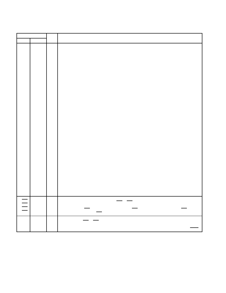
2≠12
Table 2≠7. PCI Address and Data Terminals
TERMINAL
I/O
DESCRIPTION
NAME
NUMBER
I/O
DESCRIPTION
AD31
AD30
AD29
AD28
AD27
AD26
AD25
AD24
AD23
AD22
AD21
AD20
AD19
AD18
AD17
AD16
AD15
AD14
AD13
AD12
AD11
AD10
AD9
AD8
AD7
AD6
AD5
AD4
AD3
AD2
AD1
AD0
T02
P05
U01
U02
T03
P06
V02
U03
W03
U04
R06
V04
W04
U05
N07
V05
W07
U08
V08
N10
R09
V09
W09
V10
W10
R10
W11
V11
U11
N11
R11
W12
I/O
PCI address/data bus. These signals make up the multiplexed PCI address and data bus on the primary
interface. During the address phase of a primary-bus PCI cycle, AD31≠AD0 contain a 32-bit address or other
destination information. During the data phase, AD31≠AD0 contain data.
C/BE3
C/BE2
C/BE1
C/BE0
W02
R07
P09
U10
I/O
PCI-bus commands and byte enables. These signals are multiplexed on the same PCI terminals. During the
address phase of a primary-bus PCI cycle, C/BE3≠C/BE0 define the bus command. During the data phase, this
4-bit bus is used as byte enables. The byte enables determine which byte paths of the full 32-bit data bus carry
meaningful data. C/BE0 applies to byte 0 (AD7≠AD0), C/BE1 applies to byte 1 (AD15≠AD8), C/BE2 applies to
byte 2 (AD23≠AD16), and C/BE3 applies to byte 3 (AD31≠AD24).
PAR
N09
I/O
PCI-bus parity. In all PCI-bus read and write cycles, the PCI7x20 device calculates even parity across the
AD31≠AD0 and C/BE3≠C/BE0 buses. As an initiator during PCI cycles, the PCI7x20 device outputs this parity
indicator with a one-PCLK delay. As a target during PCI cycles, the PCI7x20 device compares its calculated
parity to the parity indicator of the initiator. A compare error may result in the assertion of a parity error (PERR).
2≠13
Table 2≠8. PCI Interface Control Terminals
TERMINAL
I/O
DESCRIPTION
NAME
NUMBER
I/O
DESCRIPTION
DEVSEL
R08
I/O
PCI device select. The PCI7x20 device asserts DEVSEL to claim a PCI cycle as the target device. As a PCI
initiator on the bus, the PCI7x20 device monitors DEVSEL until a target responds. If no target responds before
timeout occurs, then the PCI7x20 device terminates the cycle with an initiator abort.
FRAME
W05
I/O
PCI cycle frame. FRAME is driven by the initiator of a bus cycle. FRAME is asserted to indicate that a bus
transaction is beginning, and data transfers continue while this signal is asserted. When FRAME is deasserted,
the PCI bus transaction is in the final data phase.
GNT
R02
I
PCI bus grant. GNT is driven by the PCI bus arbiter to grant the PCI7x20 device access to the PCI bus after
the current data transaction has completed. GNT may or may not follow a PCI bus request, depending on the
PCI bus parking algorithm.
IDSEL
V03
I
Initialization device select. IDSEL selects the PCI7x20 device during configuration space accesses. IDSEL can
be connected to one of the upper 24 PCI address lines on the PCI bus.
IRDY
U06
I/O
PCI initiator ready. IRDY indicates the ability of the PCI bus initiator to complete the current data phase of the
transaction. A data phase is completed on a rising edge of PCLK where both IRDY and TRDY are asserted. Until
IRDY and TRDY are both sampled asserted, wait states are inserted.
PERR
U07
I/O
PCI parity error indicator. PERR is driven by a PCI device to indicate that calculated parity does not match PAR
when PERR is enabled through bit 6 of the command register (PCI offset 04h, see Section 4.4).
REQ
T01
O
PCI bus request. REQ is asserted by the PCI7x20 device to request access to the PCI bus as an initiator.
SERR
V07
O
PCI system error. SERR is an output that is pulsed from the PCI7x20 device when enabled through bit 8 of the
command register (PCI offset 04h, see Section 4.4) indicating a system error has occurred. The PCI7x20 device
need not be the target of the PCI cycle to assert this signal. When SERR is enabled in the command register,
this signal also pulses, indicating that an address parity error has occurred on a CardBus interface.
STOP
W06
I/O
PCI cycle stop signal. STOP is driven by a PCI target to request the initiator to stop the current PCI bus
transaction. STOP is used for target disconnects and is commonly asserted by target devices that do not support
burst data transfers.
TRDY
V06
I/O
PCI target ready. TRDY indicates the ability of the primary bus target to complete the current data phase of the
transaction. A data phase is completed on a rising edge of PCLK when both IRDY and TRDY are asserted. Until
both IRDY and TRDY are asserted, wait states are inserted.

2≠14
Table 2≠9. Multifunction and Miscellaneous Terminals
TERMINAL
I/O
DESCRIPTION
NAME
NUMBER
I/O
DESCRIPTION
CLK_48
L02
I
Reserved for future 48-MHz clock terminal
MFUNC0
M03
I/O
Multifunction terminal 0. See Section 4.36, Multifunction Routing Status Register, for configuration
details.
MFUNC1
L06
I/O
Multifunction terminal 1. See Section 4.36, Multifunction Routing Status Register, for configuration
details.
MFUNC2
N01
I/O
Multifunction terminal 2. See Section 4.36, Multifunction Routing Status Register, for configuration
details.
MFUNC3
N02
I/O
Multifunction terminal 3. See Section 4.36, Multifunction Routing Status Register, for configuration
details.
MFUNC4
N03
I/O
Multifunction terminal 4. See Section 4.36, Multifunction Routing Status Register, for configuration
details.
MFUNC5
M05
I/O
Multifunction terminal 5. See Section 4.36, Multifunction Routing Status Register, for configuration
details.
MFUNC6
P01
I/O
Multifunction terminal 6. See Section 4.36, Multifunction Routing Status Register, for configuration
details.
PHY_TEST_MA
R17
I
PHY test pin. Not for customer use. It must be pulled high with a 4.7-k
resistor.
RI_OUT/PME
R03
O
Ring indicate out and power management event output. This terminal provides an output for
ring-indicate or PME signals.
RSVD
H05, J05,
J06, K01,
K02, K03
Reserved. These terminals have no connection anywhere within the package.
SCL
K07
I/O
Serial clock. At PRST, the SCL signal is sampled to determine if a two-wire serial ROM is present. If
the serial ROM is detected, then this terminal provides the serial clock signaling and is implemented
as open-drain. For normal operation (a ROM is implemented in the design), this terminal must be pulled
high to the ROM VDD with a 2.7-k
resistor. Otherwise, it must be pulled low to ground with a 220-
resistor.
SDA
L03
I/O
Serial data. This terminal is implemented as open-drain, and for normal operation (a ROM is
implemented in the design), this terminal must be pulled high to the ROM VDD with a 2.7-k
resistor.
Otherwise, it must be pulled low to ground with a 220-
resistor.
SPKROUT
L07
O
Speaker output. SPKROUT is the output to the host system that can carry SPKR or CAUDIO through
the PCI7x20 device from the PC Card interface. SPKROUT is driven as the exclusive-OR combination
of card SPKR//CAUDIO inputs.
SUSPEND
P02
I
Suspend. SUSPEND protects the internal registers from clearing when the GRST or PRST signal is
asserted. See Section 3.9.6, Suspend Mode, for details.
TEST0
R19
I/O
Terminal TEST0 is used for factory test of the device and must be connected to ground for normal
operation.

2≠15
Table 2≠10. 16-Bit PC Card Address and Data Terminals
SOCKET A TERMINAL
SOCKET B TERMINAL
I/O
DESCRIPTION
NAME
NUMBER
NAME
NUMBER
I/O
DESCRIPTION
A_A25
A_A24
A_A23
A_A22
A_A21
A_A20
A_A19
A_A18
A_A17
A_A16
A_A15
A_A14
A_A13
A_A12
A_A11
A_A10
A_A9
A_A8
A_A7
A_A6
A_A5
A_A4
A_A3
A_A2
A_A1
A_A0
A06
B07
E08
C08
A08
G09
B09
E10
B10
B08
F09
C09
A09
A07
B11
C12
F10
C10
C07
B06
A05
B05
C05
E06
A03
B03
B_A25
B_A24
B_A23
B_A22
B_A21
B_A20
B_A19
B_A18
B_A17
B_A16
B_A15
B_A14
B_A13
B_A12
B_A11
B_A10
B_A9
B_A8
B_A7
B_A6
B_A5
B_A4
B_A3
B_A2
B_A1
B_A0
H14
H15
G18
H13
H18
J15
J17
K15
K18
H17
G19
J13
J18
G17
L18
M18
K14
K17
F19
F17
G15
E18
F15
C19
D17
F14
O
PC Card address. 16-bit PC Card address lines. A25 is the most significant
bit.
A_D15
A_D14
A_D13
A_D12
A_D11
A_D10
A_D9
A_D8
A_D7
A_D6
A_D5
A_D4
A_D3
A_D2
A_D1
A_D0
A12
A13
B13
B14
C14
E03
D01
D03
E12
C13
A14
F12
A15
F05
D02
E05
B_D15
B_D14
B_D13
B_D12
B_D11
B_D10
B_D9
B_D8
B_D7
B_D6
B_D5
B_D4
B_D3
B_D2
B_D1
B_D0
M19
N19
N17
M14
P18
E13
A16
B16
L13
N18
M15
P19
P17
C15
E14
A17
I/O
PC Card data. 16-bit PC Card data lines. D15 is the most significant bit.
2≠16
Table 2≠11. 16-Bit PC Card Interface Control Terminals
SOCKET A TERMINAL
SOCKET B TERMINAL
I/O
DESCRIPTION
NAME
NUMBER
NAME
NUMBER
I/O
DESCRIPTION
A_BVD1
(STSCHG/RI)
C03
B_BVD1
(STSCHG/RI)
A18
I
Battery voltage detect 1. BVD1 is generated by 16-bit memory PC Cards that
include batteries. BVD1 is used with BVD2 as an indication of the condition
of the batteries on a memory PC Card. Both BVD1 and BVD2 are high when
the battery is good. When BVD2 is low and BVD1 is high, the battery is weak
and must be replaced. When BVD1 is low, the battery is no longer
serviceable and the data in the memory PC Card is lost. See Section 5.6,
ExCA Card Status-Change Interrupt Configuration Register, for enable bits.
See Section 5.5, ExCA Card Status-Change Register, and Section 5.2,
ExCA Interface Status Register, for the status bits for this signal.
Status change. STSCHG is used to alert the system to a change in the
READY, write protect, or battery voltage dead condition of a 16-bit I/O PC
Card.
Ring indicate. RI is used by 16-bit modem cards to indicate a ring detection.
A_BVD2
(SPKR)
B01
B_BVD2
(SPKR)
C17
I
Battery voltage detect 2. BVD2 is generated by 16-bit memory PC Cards that
include batteries. BVD2 is used with BVD1 as an indication of the condition
of the batteries on a memory PC Card. Both BVD1 and BVD2 are high when
the battery is good. When BVD2 is low and BVD1 is high, the battery is weak
and must be replaced. When BVD1 is low, the battery is no longer
serviceable and the data in the memory PC Card is lost. See Section 5.6,
ExCA Card Status-Change Interrupt Configuration Register, for enable bits.
See Section 5.5, ExCA Card Status-Change Register, and Section 5.2,
ExCA Interface Status Register, for the status bits for this signal.
Speaker. SPKR is an optional binary audio signal available only when the
card and socket have been configured for the 16-bit I/O interface. The audio
signals from cards A and B are combined by the PCI7x20 device and are
output on SPKROUT.
A_CD1
A_CD2
B15
C01
B_CD1
B_CD2
N15
C16
I
Card detect 1 and card detect 2. CD1 and CD2 are internally connected to
ground on the PC Card. When a PC Card is inserted into a socket, CD1 and
CD2 are pulled low. For signal status, see Section 5.2, ExCA Interface
Status Register.
A_CE1
A_CE2
B12
E11
B_CE1
B_CE2
M17
L15
O
Card enable 1 and card enable 2. CE1 and CE2 enable even- and
odd-numbered address bytes. CE1 enables even-numbered address bytes,
and CE2 enables odd-numbered address bytes.
A_INPACK
F06
B_INPACK
E17
I
Input acknowledge. INPACK is asserted by the PC Card when it can respond
to an I/O read cycle at the current address.
A_IORD
C11
B_IORD
L17
O
I/O read. IORD is asserted by the PCI7x20 device to enable 16-bit I/O PC
Card data output during host I/O read cycles.
A_IOWR
G10
B_IOWR
K13
O
I/O write. IOWR is driven low by the PCI7x20 device to strobe write data into
16-bit I/O PC Cards during host I/O write cycles.
A_OE
A11
B_OE
L19
O
Output enable. OE is driven low by the PCI7x20 device to enable 16-bit
memory PC Card data output during host memory read cycles.
A_READY
(IREQ)
A02
B_READY
(IREQ)
B19
I
Ready. The ready function is provided when the 16-bit PC Card and the host
socket are configured for the memory-only interface. READY is driven low
by 16-bit memory PC Cards to indicate that the memory card circuits are
busy processing a previous write command. READY is driven high when the
16-bit memory PC Card is ready to accept a new data transfer command.
Interrupt request. IREQ is asserted by a 16-bit I/O PC Card to indicate to the
host that a device on the 16-bit I/O PC Card requires service by the host
software. IREQ is high (deasserted) when no interrupt is requested.
2≠17
Table 2≠11. 16-Bit PC Card Interface Control Terminals (Continued)
SOCKET A TERMINAL
SOCKET B TERMINAL
I/O
DESCRIPTION
NAME
NUMBER
NAME
NUMBER
I/O
DESCRIPTION
A_REG
B04
B_REG
D18
O
Attribute memory select. REG remains high for all common memory accesses.
When REG is asserted, access is limited to attribute memory (OE or WE active)
and to the I/O space (IORD or IOWR active). Attribute memory is a separately
accessed section of card memory and is generally used to record card capacity
and other configuration and attribute information.
A_RESET
C06
B_RESET
E19
O
PC Card reset. RESET forces a hard reset to a 16-bit PC Card.
A_VS1
A_VS2
C04
E07
B_VS1
B_VS2
C18
F18
I/O
Voltage sense 1 and voltage sense 2. VS1 and VS2, when used in conjunction
with each other, determine the operating voltage of the PC Card.
A_WAIT
B02
B_WAIT
B18
I
Bus cycle wait. WAIT is driven by a 16-bit PC Card to extend the completion
of the memory or I/O cycle in progress.
A_WE
E09
B_WE
H19
O
Write enable. WE is used to strobe memory write data into 16-bit memory PC
Cards. WE is also used for memory PC Cards that employ programmable
memory technologies.
A_WP
(IOIS16)
C02
B_WP
(IOIS16)
B17
I
Write protect. WP applies to 16-bit memory PC Cards. WP reflects the status
of the write-protect switch on 16-bit memory PC Cards. For 16-bit I/O cards, WP
is used for the 16-bit port (IOIS16) function.
I/O is 16 bits. IOIS16 applies to 16-bit I/O PC Cards. IOIS16 is asserted by the
16-bit PC Card when the address on the bus corresponds to an address to
which the 16-bit PC Card responds, and the I/O port that is addressed is
capable of 16-bit accesses.
Table 2≠12. CardBus PC Card Interface System Terminals
SOCKET A TERMINAL
SOCKET B TERMINAL
I/O
DESCRIPTION
NAME
NUMBER
NAME
NUMBER
I/O
DESCRIPTION
A_CCLK
B08
B_CCLK
H17
O
CardBus clock. CCLK provides synchronous timing for all transactions on
the CardBus interface. All signals except CRST, CCLKRUN, CINT,
CSTSCHG, CAUDIO, CCD2, CCD1, CVS2, and CVS1 are sampled on the
rising edge of CCLK, and all timing parameters are defined with the rising
edge of this signal. CCLK operates at the PCI bus clock frequency, but it can
be stopped in the low state or slowed down for power savings.
A_CCLKRUN
C02
B_CCLKRUN
B17
I/O
CardBus clock run. CCLKRUN is used by a CardBus PC Card to request an
increase in the CCLK frequency, and by the PCI7x20 device to indicate that
the CCLK frequency is going to be decreased.
A_CRST
C06
B_CRST
E19
O
CardBus reset. CRST brings CardBus PC Card-specific registers,
sequencers, and signals to a known state. When CRST is asserted, all
CardBus PC Card signals are placed in a high-impedance state, and the
PCI7x20 device drives these signals to a valid logic level. Assertion can be
asynchronous to CCLK, but deassertion must be synchronous to CCLK.

2≠18
Table 2≠13. CardBus PC Card Address and Data Terminals
SOCKET A TERMINAL
SOCKET B TERMINAL
I/O
DESCRIPTION
NAME
NUMBER
NAME
NUMBER
I/O
DESCRIPTION
A_CAD31
A_CAD30
A_CAD29
A_CAD28
A_CAD27
A_CAD26
A_CAD25
A_CAD24
A_CAD23
A_CAD22
A_CAD21
A_CAD20
A_CAD19
A_CAD18
A_CAD17
A_CAD16
A_CAD15
A_CAD14
A_CAD13
A_CAD12
A_CAD11
A_CAD10
A_CAD9
A_CAD8
A_CAD7
A_CAD6
A_CAD5
A_CAD4
A_CAD3
A_CAD2
A_CAD1
A_CAD0
E03
D01
D02
D03
E05
B03
A03
E06
C05
B05
A05
B06
A06
C07
B07
B10
G10
F10
C11
B11
A11
E11
C12
A12
E12
B13
C13
B14
A14
C14
F12
A15
B_CAD31
B_CAD30
B_CAD29
B_CAD28
B_CAD27
B_CAD26
B_CAD25
B_CAD24
B_CAD23
B_CAD22
B_CAD21
B_CAD20
B_CAD19
B_CAD18
B_CAD17
B_CAD16
B_CAD15
B_CAD14
B_CAD13
B_CAD12
B_CAD11
B_CAD10
B_CAD9
B_CAD8
B_CAD7
B_CAD6
B_CAD5
B_CAD4
B_CAD3
B_CAD2
B_CAD1
B_CAD0
E13
A16
E14
B16
A17
F14
D17
C19
F15
E18
G15
F17
H14
F19
H15
K18
K13
K14
L17
L18
L19
L15
M18
M19
L13
N17
N18
M14
M15
P18
P19
P17
I/O
CardBus address and data. These signals make up the multiplexed CardBus
address and data bus on the CardBus interface. During the address phase of
a CardBus cycle, CAD31≠CAD0 contain a 32-bit address. During the data
phase of a CardBus cycle, CAD31≠CAD0 contain data. CAD31 is the most
significant bit.
A_CC/BE3
A_CC/BE2
A_CC/BE1
A_CC/BE0
B04
A07
C10
B12
B_CC/BE3
B_CC/BE2
B_CC/BE1
B_CC/BE0
D18
G17
K17
M17
I/O
CardBus bus commands and byte enables. CC/BE3≠CC/BE0 are multiplexed
on the same CardBus terminals. During the address phase of a CardBus cycle,
CC/BE3≠CC/BE0 define the bus command. During the data phase, this 4-bit
bus is used as byte enables. The byte enables determine which byte paths of
the full 32-bit data bus carry meaningful data. CC/BE0 applies to byte 0
(CAD7≠CAD0), CC/BE1 applies to byte 1 (CAD15≠CAD8), CC/BE2 applies to
byte 2 (CAD23≠CAD16), and CC/BE3 applies to byte 3 (CAD31≠CAD24).
A_CPAR
A09
B_CPAR
J18
I/O
CardBus parity. In all CardBus read and write cycles, the PCI7x20 device
calculates even parity across the CAD and CC/BE buses. As an initiator during
CardBus cycles, the PCI7x20 device outputs CPAR with a one-CCLK delay. As
a target during CardBus cycles, the PCI7x20 device compares its calculated
parity to the parity indicator of the initiator; a compare error results in a parity
error assertion.
2≠19
Table 2≠14. CardBus PC Card Interface Control Terminals
SOCKET A TERMINAL
SOCKET B TERMINAL
I/O
DESCRIPTION
NAME
NUMBER
NAME
NUMBER
I/O
DESCRIPTION
A_CAUDIO
B01
B_CAUDIO
C17
I
CardBus audio. CAUDIO is a digital input signal from a PC Card to the
system speaker. The PCI7x20 device supports the binary audio mode and
outputs a binary signal from the card to SPKROUT.
A_CBLOCK
B09
B_CBLOCK
J17
I/O
CardBus lock. CBLOCK is used to gain exclusive access to a target.
A_CCD1
B15
B_CCD1
N15
I
CardBus detect 1 and CardBus detect 2. CCD1 and CCD2 are used in
j
ti
ith CVS1
d CVS2 t id
tif
d i
ti
d i t
t
A_CCD1
A_CCD2
B15
C01
B_CCD1
B_CCD2
N15
C16
I
conjunction with CVS1 and CVS2 to identify card insertion and interrogate
cards to determine the operating voltage and card type.
A_CDEVSEL
A08
B_CDEVSEL
H18
I/O
CardBus device select. The PCI7x20 device asserts CDEVSEL to claim a
CardBus cycle as the target device. As a CardBus initiator on the bus, the
PCI7x20 device monitors CDEVSEL until a target responds. If no target
responds before timeout occurs, then the PCI7x20 device terminates the
cycle with an initiator abort.
A_CFRAME
E08
B_CFRAME
G18
I/O
CardBus cycle frame. CFRAME is driven by the initiator of a CardBus bus
cycle. CFRAME is asserted to indicate that a bus transaction is beginning,
and data transfers continue while this signal is asserted. When CFRAME is
deasserted, the CardBus bus transaction is in the final data phase.
A_CGNT
E09
B_CGNT
H19
O
CardBus bus grant. CGNT is driven by the PCI7x20 device to grant a
CardBus PC Card access to the CardBus bus after the current data
transaction has been completed.
A_CINT
A02
B_CINT
B19
I
CardBus interrupt. CINT is asserted low by a CardBus PC Card to request
interrupt servicing from the host.
A_CIRDY
F09
B_CIRDY
G19
I/O
CardBus initiator ready. CIRDY indicates the ability of the CardBus initiator
to complete the current data phase of the transaction. A data phase is
completed on a rising edge of CCLK when both CIRDY and CTRDY are
asserted. Until CIRDY and CTRDY are both sampled asserted, wait states
are inserted.
A_CPERR
C09
B_CPERR
J13
I/O
CardBus parity error. CPERR reports parity errors during CardBus
transactions, except during special cycles. It is driven low by a target two
clocks following the data cycle during which a parity error is detected.
A_CREQ
F06
B_CREQ
E17
I
CardBus request. CREQ indicates to the arbiter that the CardBus PC Card
desires use of the CardBus bus as an initiator.
A_CSERR
B02
B_CSERR
B18
I
CardBus system error. CSERR reports address parity errors and other
system errors that could lead to catastrophic results. CSERR is driven by the
card synchronous to CCLK, but deasserted by a weak pullup; deassertion
may take several CCLK periods. The PCI7x20 device can report CSERR to
the system by assertion of SERR on the PCI interface.
A_CSTOP
G09
B_CSTOP
J15
I/O
CardBus stop. CSTOP is driven by a CardBus target to request the initiator
to stop the current CardBus transaction. CSTOP is used for target
disconnects, and is commonly asserted by target devices that do not support
burst data transfers.
A_CSTSCHG
C03
B_CSTSCHG
A18
I
CardBus status change. CSTSCHG alerts the system to a change in the
card status, and is used as a wake-up mechanism.
A_CTRDY
C08
B_CTRDY
H13
I/O
CardBus target ready. CTRDY indicates the ability of the CardBus target to
complete the current data phase of the transaction. A data phase is
completed on a rising edge of CCLK, when both CIRDY and CTRDY are
asserted; until this time, wait states are inserted.
A_CVS1
A_CVS2
C04
E07
B_CVS1
B_CVS2
C18
F18
I/O
CardBus voltage sense 1 and CardBus voltage sense 2. CVS1 and CVS2
are used in conjunction with CCD1 and CCD2 to identify card insertion and
interrogate cards to determine the operating voltage and card type.

2≠20
Table 2≠15. IEEE 1394 Physical Layer Terminals
TERMINAL
I/O
DESCRIPTION
NAME
NUMBER
I/O
DESCRIPTION
CNA
R18
I/O
Cable not active. This terminal is asserted high when there are no ports receiving incoming bias voltage.
If it is not used, then this terminal must be strapped to GND through a resistor.
CPS
P12
I
Cable power status input. This terminal is normally connected to cable power through a 400-k
resistor.
This circuit drives an internal comparator that is used to detect the presence of cable power. If CPS is not
used to detect cable power, then this terminal must be pulled to AVDx.
FILTER0
FILTER1
U17
U18
I/O
PLL filter terminals. These terminals are connected to an external capacitance to form a lag-lead filter
required for stable operation of the internal frequency multiplier PLL running off of the crystal oscillator. A
0.1-
µ
F
±
10% capacitor is the only external component required to complete this filter.
PC0
PC1
PC2
N12
U12
V12
I
Power class programming inputs. On hardware reset, these inputs set the default value of the power class
indicated during self-ID. Programming is done by tying these terminals high or low.
R0
R1
W15
V15
≠
Current-setting resistor terminals. These terminals are connected to an external resistance to set the
internal operating currents and cable driver output currents. A resistance of 6.34 k
±
1% is required to meet
the IEEE Std 1394-1995 output voltage limits.
TPA0P
TPA0N
V14
W14
I/O
Twisted-pair cable A differential signal terminals. Board trace lengths from each pair of positive and negative
diff
ti l i
l i
t b
t h d
d
h t
ibl t th
t
l l
d
i t
d t th
TPA1P
TPA1N
V18
W18
I/O
differential signal pins must be matched and as short as possible to the external load resistors and to the
cable connector. For an unused port, TPA+ and TPA≠ can be left open.
TPBIAS0
TPBIAS1
U14
V19
I/O
Twisted-pair bias output. This provides the 1.86-V nominal bias voltage needed for proper operation of the
twisted-pair cable drivers and receivers and for signaling to the remote nodes that there is an active cable
connection. Each of these pins must be decoupled with a 1.0-
µ
F capacitor to ground.
TPB0P
TPB0N
V13
W13
I/O
Twisted-pair cable B differential signal terminals. Board trace lengths from each pair of positive and negative
diff
ti l i
l i
t b
t h d
d
h t
ibl t th
t
l l
d
i t
d t th
TPB1P
TPB1N
V16
W16
I/O
differential signal pins must be matched and as short as possible to the external load resistors and to the
cable connector. For an unused port, TPB+ and TPB≠ must be pulled to ground.
XI
XO
T18
T19
≠
Crystal oscillator inputs. These pins connect to a 24.576-MHz parallel resonant fundamental mode crystal.
The optimum values for the external shunt capacitors are dependent on the specifications of the crystal
used (see Section 3.10.2, Crystal Selection). Terminal 5 has an internal 10-k
(nominal value) pulldown
resistor. An external clock input can be connected to the XI terminal. When using an external clock input,
the XO terminal must be left unconnected, and the clock must be supplied before the device is taken out
of reset. Refer to Section 3.10.2 for the operating characteristics of the XI terminal.
Table 2≠16. MMC/SD Terminals
TERMINAL
I/O
DESCRIPTION
NAME
NUMBER
I/O
DESCRIPTION
MC_CD_0
E02
I
Media Card detect. This input is asserted when MMC/SD media are inserted.
MC_PWR_CTRL_0
F01
O
Media card power control for MMC/SD socket.
SD_DAT3
SD_DAT2
SD_DAT1
SD_DAT0
J02
J01
J07
H03
I/O
SD flash data [3:0]. These signals provide the SD data path per the SD Memory Card
Specifications.
SD_CMD
H02
I/O
SD flash command. This signal provides the SD command per the SD Memory Card
Specifications.
SD_CLK
H01
I/O
SD flash clock. This output provides the MMC/SD clock, which operates at 16 MHz.
SD_WP
J03
I
SD write protect data. This signal indicates that the media inserted in the socket is write
protected.

2≠21
Table 2≠17. Memory Stick Terminals
TERMINAL
I/O
DESCRIPTION
NAME
NUMBER
I/O
DESCRIPTION
MC_CD_1
E01
I
Media Card detect. This input is asserted when a Memory Stick or Memory Stick Pro media is
inserted.
MC_PWR_CTRL_1
F03
O
Media card power control for Memory Stick and Memory Stick Pro socket.
MS_DATA3
MS_DATA2
MS_DATA1
H07
G03
G02
I/O
Memory Stick data [3:1]. These signals provide the Memory Stick data path.
MS_SDIO (DATA0)
G01
I/O
Memory Stick serial data I/O. This signal provides Memory Stick data input/output. Memory
Stick data 0.
MS_CLK
G05
I/O
Memory Stick clock. This output provides the MS clock, which operates at 16 MHz.
MS_BS
F02
I/O
Memory Stick bus state. This signal provides Memory Stick bus state information.

2≠22
Smart Card defines additional functionality for the CardBus/PC Card terminals. Table 2≠18 gives the signal names
and mapping of this additional functionality to the PCI7x20 CardBus/PC Card terminals, with reference to the 68-pin
card socket. Table 2≠19 provides the signal descriptions.
Table 2≠18. Smart Card Mapping to the PCMCIA 68-Terminal Connector
TERM.
16-Bit PC Card
CardBus
Smart Card
TERM.
16-Bit PC Card
CardBus
Smart Card
1
GND
GND
GND
35
GND
GND
GND
2
D3
CAD0
RSVD
36
CD1
CCD1
CCD1
3
D4
CAD1
RSVD
37
D11
CAD2
RSVD
4
D5
CAD3
RSVD
38
D12
CAD4
RSVD
5
D6
CAD5
RSVD
39
D13
CAD6
RSVD
6
D7
CAD7
RSVD
40
D14
RFU
RSVD
7
CE1
CC/BE0
RSVD
41
D15
CAD8
RSVD
8
A10
CAD9
RSVD
42
CE2
CAD10
RSVD
9
OE
CAD11
RSVD
43
VS1
CVS1
CVS1
10
A11
CAD12
RSVD
44
IORD/RFU
CAD13
RSVD
11
A9
CAD14
RSVD
45
IOWR/RFU
CAD15
RSVD
12
A8
CC/BE1
RSVD
46
A17
CAD16
RSVD
13
A13
CPAR
RSVD
47
A18
RFU
SQRY1
14
A14
CPERR
RSVD
48
A19
CBLOCK
RSVD
15
WE
CGNT
SC_RFU
49
A20
CSTOP
RSVD
16
READY/IREQ
CINT
RSVD
50
A21
CDEVSEL
RSVD
17
VCC
VCC
VCC
51
VCC
VCC
VCC
18
VPP/VCORE
VPP/VCORE
VPP/VCORE
52
VPP/VCORE
VPP/VCORE
VPP/VCORE
19
A16
CCLK
SC_CLK
53
A22
CTRDY
MC_CD
20
A15
CIRDY
RSVD
54
A23
CFRAME
SC_FCB
21
A12
CC/BE2
SC_RST
55
A24
CAD17
SC_I/O
22
A7
CAD18
SC_GPIO0
56
A25
CAD19
SQRYDR
23
A6
CAD20
SC_GPIO1
57
VS2
CVS2
CVS2
24
A5
CAD21
SC_GPIO2
58
RESET
CRST
SQRY2
25
A4
CAD22
SC_GPIO3
59
WAIT
CSERR
SQRY3
26
A3
CAD23
SC_GPIO4
60
INPACK/RFU
CREQ
SQRY4
27
A2
CAD24
SC_GPIO5
61
REG
CC/BE3
SQRY5
28
A1
CAD25
SC_GPIO06
62
BVD2(SPKR)
CAUDIO
SQRY6
29
A0
CAD26
SC_GPIO7
63
BVD1(STSCHG/RI)
CSTSCHG
SQRY7
30
D0
CAD27
RSVD
64
D8
CAD28
SQRY8
31
D1
CAD29
RSVD
65
D9
CAD30
SQRY9
32
D2
RFU
RSVD
66
D10
CAD31
SQRY10
33
WP(IOIS16)
CCLKRUN
RSVD
67
CD2
CCD2
CCD2
34
GND
GND
GND
68
GND
GND
GND

2≠23
Table 2≠19. Smart Card Terminals (Sockets A and B)
TERMINAL
NAME
NUMBER
I/O
DESCRIPTION
NAME
SOCKET A
SOCKET B
I/O
DESCRIPTION
SC_CLK
B08
H17
O
Smart Card clock. The PCI7x20 device drives a 3-MHz clock to the Smart Card interface
when enabled.
SC_FCB
E08
G18
I
Smart Card function code. The PCI7x20 device does not support synchronous Smart
Cards as specified in ISO/IEC 7816-10, and this terminal is in a high-impedance state
when an UltraMedia Smart Card adapter has been inserted.
SC_GPIO0
C07
F19
I/O
SC_GPIO1
B06
F17
I/O
SC_GPIO2
A05
G15
I/O
SC_GPIO3
B05
E18
I/O
Smart Card general-purpose I/O terminals. These signals can be controlled by firmware
SC_GPIO4
C05
F15
I/O
Smart Card general ur ose I/O terminals. These signals can be controlled by firmware
and are used as control signals for an external Smart Card interface chip or level shifter.
SC_GPIO5
E06
C19
I/O
g
SC_GPIO6
A03
D17
I/O
SC_GPIO7
B03
F14
I/O
SC_IO
B07
H15
I/O
Smart Card input/output. This terminal is the input/output terminal for the character
exchange between the PCI7x20 device and the Smart Cards.
SC_RFU
E09
H19
I
Smart Card reserved. This terminal is in a high-impedance state when an UltraMedia
Smart Card adapter has been inserted.
SC_RST
A07
G17
O
Smart Card reset. This signal starts and stops the Smart Card reset sequence. The
PCI7x20 device asserts this reset when requested by the host.

2≠24
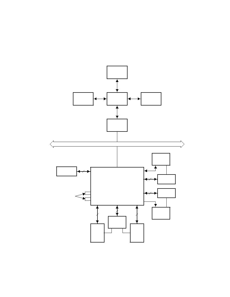
3≠1
3 Feature/Protocol Descriptions
The following sections give an overview of the PCI7x20 device. Figure 3≠1 shows the connections to the PCI7x20
device. The PCI interface includes all address/data and control signals for PCI protocol. The interrupt interface
includes terminals for parallel PCI, parallel ISA, and serialized PCI and ISA signaling.
PCI Bus
CPU
North
Bridge
Memory
South
Bridge
Graphics
Controller
PCI7x20
1394
Socket
Power
Switch
EEPROM
Power
Switch
2
8
7
MMC/
SD
MS/
MS PRO
PC
Card/
Smart
Card
Power
Switch
3
68
PC
Card/
Smart
Card
68
Figure 3≠1. PCI7x20 System Block Diagram

3≠2
3.1
Power Supply Sequencing
The PCI7x20 device contains 3.3-V I/O buffers with 5-V tolerance requiring a core power supply and clamp voltages.
The core power supply is always 1.8 V. The clamp voltages can be either 3.3 V or 5 V, depending on the interface.
The following power-up and power-down sequences are recommended.
The power-up sequence is:
1.
Apply the clamp voltage.
2.
Apply the I/O voltage.
3.
Apply the analog voltage.
4.
Power core 1.8 V.
The power-down sequence is:
1.
Remove power from the core.
2.
Remove the analog voltage.
3.
Remove the I/O voltage.
4.
Remove the clamp voltage.
NOTE: If the voltage regulator is enabled, then steps 2, 3, and 4 of the power-up sequence
and steps 1, 2, and 3 of the power-down sequence all occur simultaneously.
3.2
I/O Characteristics
The PCI7x20 device meets the ac specifications of the PC Card Standard (release 8.0) and the PCI Local Bus
Specification. Figure 3≠2 shows a 3-state bidirectional buffer. Section 12.2, Recommended Operating Conditions,
provides the electrical characteristics of the inputs and outputs.
Tied for Open Drain
OE
Pad
VCCP
Figure 3≠2. 3-State Bidirectional Buffer
3.3
Clamping Voltages
The clamping voltages are set to match whatever external environment the PCI7x20 device is interfaced with: 3.3 V
or 5 V. The I/O sites can be pulled through a clamping diode to a voltage rail that protects the core from external
signals. The core power supply is 1.8 V and is independent of the clamping voltages. For example, PCI signaling can
be either 3.3 V or 5 V, and the PCI7x20 device must reliably accommodate both voltage levels. This is accomplished
by using a 3.3-V I/O buffer that is 5-V tolerant, with the applicable clamping voltage applied. If a system designer
desires a 5-V PCI bus, then V
CCP
can be connected to a 5-V power supply.
3.4
Peripheral Component Interconnect (PCI) Interface
The PCI7x20 device is fully compliant with the PCI Local Bus Specification. The PCI7x20 device provides all required
signals for PCI master or slave operation, and may operate in either a 5-V or 3.3-V signaling environment by
connecting the V
CCP
terminals to the desired voltage level. In addition to the mandatory PCI signals, the PCI7x20
device provides the optional interrupt signals INTA, INTB, INTC, and INTD.

3≠3
3.4.1
1394 PCI Bus Master
As a bus master, the 1394 function of the PCI7x20 device supports the memory commands specified in Table 3≠1.
The PCI master supports the memory read, memory read line, and memory read multiple commands. The read
command usage for read transactions of greater than two data phases are determined by the selection in bits 9≠8
(MR_ENHANCE field) of the PCI miscellaneous configuration register (refer to Section 7.22 for details). For read
transactions of one or two data phases, a memory read command is used.
Table 3≠1. PCI Bus Support
PCI
COMMAND
C/BE3≠C/BE0
OHCI MASTER FUNCTION
Memory read
0110
DMA read from memory
Memory write
0111
DMA write to memory
Memory read multiple
1100
DMA read from memory
Memory read line
1110
DMA read from memory
Memory write and invalidate
1111
DMA write to memory
3.4.2
Device Resets
During the power-up sequence, GRST and PRST must be asserted. GRST can only be deasserted 100
µ
s after PCLK
is stable. PRST can be deasserted at the same time as GRST or any time thereafter.
3.4.3
PCI Bus Lock (LOCK)
The bus-locking protocol defined in the PCI Local Bus Specification is not highly recommended, but is provided on
the PCI7x20 device as an additional compatibility feature. The PCI LOCK signal can be routed to the MFUNC4
terminal by setting the appropriate values in bits 19≠16 of the multifunction routing status register. See Section 4.36,
Multifunction Routing Status Register,
for details. Note that the use of LOCK is only supported by PCI-to-CardBus
bridges in the downstream direction (away from the processor).
PCI LOCK indicates an atomic operation that may require multiple transactions to complete. When LOCK is asserted,
nonexclusive transactions can proceed to an address that is not currently locked. A grant to start a transaction on
the PCI bus does not assure control of LOCK; control of LOCK is obtained under its own protocol. It is possible for
different initiators to use the PCI bus while a single master retains ownership of LOCK. Note that the CardBus signal
for this protocol is CBLOCK to avoid confusion with the bus clock.
An agent may need to do an exclusive operation because a critical access to memory might be broken into several
transactions, but the master wants exclusive rights to a region of memory. The granularity of the lock is defined by
PCI to be 16 bytes, aligned. The LOCK protocol defined by the PCI Local Bus Specification allows a resource lock
without interfering with nonexclusive real-time data transfer, such as video.
The PCI bus arbiter may be designed to support only complete bus locks using the LOCK protocol. In this scenario,
the arbiter does not grant the bus to any other agent (other than the LOCK master) while LOCK is asserted. A
complete bus lock may have a significant impact on the performance of the video. The arbiter that supports complete
bus LOCK must grant the bus to the cache to perform a writeback due to a snoop to a modified line when a locked
operation is in progress.
The PCI7x20 device supports all LOCK protocols associated with PCI-to-PCI bridges, as also defined for
PCI-to-CardBus bridges. This includes disabling write posting while a locked operation is in progress, which can solve
a potential deadlock when using devices such as PCI-to-PCI bridges. The potential deadlock can occur if a CardBus
target supports delayed transactions and blocks access to the target until it completes a delayed read. This target
characteristic is prohibited by the PCI Local Bus Specification, and the issue is resolved by the PCI master using
LOCK.
3.4.4
Serial EEPROM I
2
C Bus
The PCI7x20 device offers many choices for modes of operation, and these choices are selected by programming
several configuration registers. For system board applications, these registers are normally programmed through the

3≠4
BIOS routine. For add-in card and docking-station/port-replicator applications, the PCI7x20 device provides a
two-wire inter-integrated circuit (IIC or I
2
C) serial bus for use with an external serial EEPROM.
The PCI7x20 device is always the bus master, and the EEPROM is always the slave. Either device can drive the bus
low, but neither device drives the bus high. The high level is achieved through the use of pullup resistors on the SCL
and SDA signal lines. The PCI7x20 device is always the source of the clock signal, SCL.
System designers who wish to load register values with a serial EEPROM must use pullup resistors on the SCL and
SDA terminals. If the PCI7x20 device detects a logic-high level on the SCL terminal at the end of GRST, then it initiates
incremental reads from the external EEPROM. Any size serial EEPROM up to the I
2
C limit of 16 Kbits can be used,
but only the first 67 bytes (from offset 00h to offset 42h) are required to configure the PCI7x20 device. Figure 3≠3
shows a serial EEPROM application.
In addition to loading configuration data from an EEPROM, the PCI7x20 I
2
C bus can be used to read and write from
other I
2
C serial devices. A system designer can control the I
2
C bus, using the PCI7x20 device as bus master, by
reading and writing PCI configuration registers
. Setting bit 3 (SBDETECT) in the serial bus control/status register (PCI
offset B3h, see Section 4.50) causes the PCI7x20 device to route the SDA and SCL signals to the SDA and SCL
terminals, respectively. The read/write data, slave address, and byte addresses are manipulated by accessing the
serial bus data, serial bus index, and serial bus slave address registers (PCI offsets B0h, B1h, and B2h; see Sections
4.47, 4.48, and 4.49, respectively).
EEPROM interface status information is communicated through the serial bus control and status register (PCI offset
B3h, see Section 4.50). Bit 3 (SBDETECT) in this register indicates whether or not the PCI7x20 serial ROM circuitry
detects the pullup resistor on SCL. Any undefined condition, such as a missing acknowledge, results in bit 0
(ROM_ERR) being set. Bit 4 (ROMBUSY) is set while the subsystem ID register is loading (serial ROM interface is
busy).
The subsystem vendor ID for functions 2 and 3 is also loaded through EEPROM. The EEPROM load data goes to
all four functions from the serial EEPROM loader.
SCL
SDA
VCC
A0
A1
A2
SCL
SDA
PCI7x20
Serial
ROM
Figure 3≠3. Serial ROM Application
3.4.5
Functions 0 and 1 (CardBus) Subsystem Identification
The subsystem vendor ID register (PCI offset 40h, see Section 4.26) and subsystem ID register (PCI offset 42h, see
Section 4.27) make up a doubleword of PCI configuration space for functions 0 and 1. This doubleword register is
used for system and option card (mobile dock) identification purposes and is required by some operating systems.
Implementation of this unique identifier register is a PC 99/PC 2001 requirement.
The PCI7x20 device offers two mechanisms to load a read-only value into the subsystem registers. The first
mechanism relies upon the system BIOS providing the subsystem ID value. The default access mode to the

3≠5
subsystem registers is read-only, but can be made read/write by clearing bit 5 (SUBSYSRW) in the system control
register (PCI offset 80h, see Section 4.29). Once this bit is cleared, the BIOS can write a subsystem identification
value into the registers at PCI offset 40h. The BIOS must set the SUBSYSRW bit such that the subsystem vendor
ID register and subsystem ID register are limited to read-only access. This approach saves the added cost of
implementing the serial electrically erasable programmable ROM (EEPROM).
In some conditions, such as in a docking environment, the subsystem vendor ID register and subsystem ID register
must be loaded with a unique identifier via a serial EEPROM. The PCI7x20 device loads the data from the serial
EEPROM after a reset of the primary bus. Note that the SUSPEND input gates the PCI reset from the entire PCI7x20
core, including the serial-bus state machine (see Section 3.9.6, Suspend Mode, for details on using SUSPEND).
The PCI7x20 device provides a two-line serial-bus host controller that can interface to a serial EEPROM. See
Section 3.7, Serial EEPROM Interface,
for details on the two-wire serial-bus controller and applications.
3.4.6
Function 2 (OHCI 1394) Subsystem Identification
The subsystem identification register is used for system and option card identification purposes. This register can
be initialized from the serial EEPROM or programmed via the subsystem access register at offset F8h in the PCI
configuration space (see Section 7.24, Subsystem Access Register). See Table 7≠21 for a complete description of
the register contents.
Write access to the subsystem access register updates the subsystem identification registers identically to
OHCI-Lynx
.
The contents of the subsystem access register are aliased to the subsystem vendor ID and subsystem
ID registers at Function 2 PCI offsets 2Ch and 2Eh, respectively. The system ID value written to this register may also
be read back from this register. See Table 7≠21 for a complete description of the register contents.
3.4.7
Function 3 (Flash Media) Subsystem Identification
The subsystem identification register is used for system and option card identification purposes. This register can
be initialized from the serial EEPROM or programmed via the subsystem access register at offset 50h in the PCI
configuration space (see Section 11.22, Subsystem Access Register). See Table 11≠15 for a complete description
of the register contents.
The contents of the subsystem access register are aliased to the subsystem vendor ID and subsystem ID registers
at Function 3 PCI offsets 2Ch and 2Eh, respectively. See Table 11≠15 for a complete description of the register
contents.
3.5
Summary of UltraMedia
Cards
3.5.1
MultiMediaCard (MMC)
The MultiMediaCard is a flash-memory card about the size of a postage stamp and 1,4 mm in thickness. The
specification for MMC is governed by the MultiMediaCard Association (MMCA). The interface for MMC cards is based
on a 7-terminal serial bus. The MultiMediaCard system specification defines a communication protocol for MMC
cards, referred to as MultiMediaCard mode. In addition, all MMC cards work in the alternate SPI mode. The SPI mode
allows a microcontroller to interface directly to the MMC card, but at the cost of slower performance.
The voltage range for communication with MMC cards is 2.0 to 3.6 V, and the memory-access voltage range is a
card-specific subrange of the communication voltage range. Like SmartMedia cards, MMC cards can be read-only
or read/write; however, MMC cards can also have I/O functionality.
MMC cards are designed to be used in either a stand-alone implementation or in a system with other MMC cards.
When in the MultiMediaCard mode, the bus protocol can address cards with up to 64K of memory, and up to 30 cards
on a single physical bus. However, the maximum data rate is only available with up to 10 MMC cards on the bus. In
order to accommodate such a wide variety of system implementations, the MMC clock rate can be varied from 0 to
20 MHz. UltraMedia supports one MMC card per UltraMedia socket.

3≠6
MMC cards, like SmartMedia cards, are also used in many types of consumer electronic devices. Because of their
small size, they are primarily used in portable music players and phones.
3.5.2
Secure Digital (SD)
SD cards are the same size as MMC cards, except for the thickness, which at 2,1 mm is slightly thicker than an MMC
card. SD cards are based upon MMC cards, with the addition of two terminals. The use of these two terminals and
a reserved terminal on MMC cards allows the data bus on SD cards to be up to 4 bits wide instead of the 1-bit width
of the MMC data bus. SD cards can communicate in either SD mode or SPI mode.
The voltage range for basic communication with SD cards is 2.0 to 3.6 V, and the voltage range for other commands
and memory access is 2.7 to 3.6 V. SD cards can be read-only or read/write.
SD is essentially a superset of MMC, in that MMC cards work in SD systems, but SD cards do not work in current
MMC systems. Unlike MMC, each SD card in a system must have a dedicated bus. One of the primary benefits of
SD cards is the added security that they provide. SD cards comply with the highest security of SDMI, have built-in
write-protect features, and include a mechanical write-protect switch.
SD cards are used in many of the same devices as MMC cards. The additional security features of the SD cards also
allow their use in more-secure applications or in devices where content protection is essential.
3.5.3
Memory Stick/MS-Pro
Memory Stick cards are about the size of a stick of gum and are 2,8 mm thick. Developed by Sony, Memory Stick
cards have a 10-terminal interface of which three terminals are used for serial communication, two terminals apply
power, two terminals are ground, one terminal is for insertion detection, and two terminals are reserved for future use.
Each card also includes an erasure-prevention switch to protect data stored on the card.
The voltage range for Memory Stick cards is 2.7 to 3.6 V, and the clock speed can be up to 20 MHz. Memory Stick
cards use the FAT file system to allow for easy communication with PCs.
There are two types of Memory Stick cards, the standard Memory Stick and the MagicGate Memory Stick. MagicGate
technology provides security to Memory Stick cards so that they can be used to store and protect copyrighted data.
Memory Stick cards are primarily used to store still images, moving images, voice, and music. As such, they are used
in a variety of devices, including portable music players, digital cameras, and digital picture frames.
3.5.4
Smart Card
Smart Cards, also called integrated circuit cards or ICCs, are the same size as a credit card, and they contain an
embedded microprocessor chip. Smart Cards can either have contacts or be contactless. In addition, there are both
asynchronous and synchronous versions of Smart Cards with contacts. Within this data manual, all uses of the term
Smart Card refers only to asynchronous Smart Cards with contacts.
Smart Cards contain eight contacts; however, two of the contacts are reserved for future use and are not included
in the UltraMedia interface. Smarts Cards can be either 5-V or 3-V cards; however, all 3-V cards are designed to work
also at 5 V.
The primary use of Smart Cards is in security-related applications. They are also used in credit cards, debit systems,
and identification systems.
3.6
PC Card Applications
The PCI7x20 device supports all the PC Card features and applications as described below.
∑
Card insertion/removal and recognition per the PC Card Standard (release 8.0)
∑
Speaker and audio applications
∑
LED socket activity indicators

3≠7
∑
PC Card controller programming model
∑
CardBus socket registers
3.6.1
PC Card Insertion/Removal and Recognition
The PC Card Standard (release 8.0) addresses the card-detection and recognition process through an interrogation
procedure that the socket must initiate on card insertion into a cold, nonpowered socket. Through this interrogation,
card voltage requirements and interface (16-bit versus CardBus) are determined.
The scheme uses the card-detect and voltage-sense signals. The configuration of these four terminals identifies the
card type and voltage requirements of the PC Card interface.
3.6.2
Low Voltage CardBus Card Detection
The card detection logic of the PCI7x20 device includes the detection of Cardbus cards with V
CC
= 3.3 V and
V
PP
= 1.8 V. The reporting of the 1.8-V CardBus card (V
CC
= 3.3 V, V
PP
= 1.8 V) is reported through the socket present
state register as follows based on bit 10 (12V_SW_SEL) in the general control register (PCI offset 86h, see Section
4.31):
∑
If the 12V_SW_SEL bit is 0 (TPS2228 is used), then the 1.8-V CardBus card causes the 3VCARD bit in the
socket present state register to be set.
∑
If the 12V_SW_SEL bit is 1 (TPS2226 is used), then the 1.8-V CardBus card causes the XVCARD bit in
the socket present state register to be set.
3.6.3
UltraMedia Card Detection
The PCI7x20 device is capable of detecting all the UltraMedia devices defined by the PCMCIA Proposal 0262 ≠
MultiMedia Cards, Secure Digital, Memory Stick devices, and Smart Card devices. The detection of these devices
is made possible through circuitry included in the PCI7x20 device and the adapters used to interface these devices
with the PC Card/CardBus sockets. No additional hardware requirements are placed on the system designer in order
to support these devices.
The PC Card Standard addresses the card detection and recognition process through an interrogation procedure that
the socket must initiate upon card insertion into a cold, unpowered socket. Through this interrogation, card voltage
requirements and interface type (16-bit vs. CardBus) are determined. The scheme uses the CD1, CD2, VS1, and VS2
signals (CCD1, CCD2, CVS1, CVS2 for CardBus). A PC Card designer connects these four terminals in a certain
configuration to indicate the type of card and its supply voltage requirements. The encoding scheme for this, defined
in the PC Card Standard, is shown in Table 3≠2.

3≠8
Table 3≠2. PC Card--Card Detect and Voltage Sense Connections
CD2//CCD2
CD1//CCD1
VS2//CVS2
VS1//CVS1
Key
Interface
VCC
VPP/VCORE
Ground
Ground
Open
Open
5 V
16-bit PC Card
5 V
Per CIS (VPP)
Ground
Ground
Open
Ground
5 V
16-bit PC Card
5 V and 3.3 V
Per CIS (VPP)
Ground
Ground
Ground
Ground
5 V
16-bit PC Card
5 V, 3.3 V, and
X.X V
Per CIS (VPP)
Ground
Ground
Open
Ground
LV
16-bit PC Card
3.3 V
Per CIS (VPP)
Ground
Connect to
CVS1
Open
Connect to
CCD1
LV
CardBus PC Card
3.3 V
Per CIS (VPP)
Ground
Ground
Ground
Ground
LV
16-bit PC Card
3.3 V and X.X V
Per CIS (VPP)
Connect to
CVS2
Ground
Connect to
CCD2
Ground
LV
CardBus PC Card
3.3 V and X.X V
Per CIS (VPP)
Connect to
CVS1
Ground
Ground
Connect to
CCD2
LV
CardBus PC Card
3.3 V, X.X V,
and Y.Y V
Per CIS (VPP)
Ground
Ground
Ground
Open
LV
16-bit PC Card
X.X V
Per CIS (VPP)
Connect to
CVS2
Ground
Connect to
CCD2
Open
LV
CardBus PC Card
3.3 V
1.8 V (VCORE)
Ground
Connect to
CVS2
Connect to
CCD1
Open
LV
CardBus PC Card
X.X V and Y.Y V
Per CIS (VPP)
Connect to
CVS1
Ground
Open
Connect to
CCD2
LV
CardBus PC Card
Y.Y V
Per CIS (VPP)
Ground
Connect to
CVS1
Ground
Connect to
CCD1
LV
UltraMedia
Per query terminals
Ground
Connect to
CVS2
Connect to
CCD1
Ground
Reserved
Reserved
3.6.4
Flash Media Card Detection
The PCI7x20 device detects an MMC/SD card insertion through the MC_CD_0 terminal. When this terminal is 0, an
MMC/SD card is inserted in the socket. The PCI7x20 device debounces the MC_CD_0 signal such that instability
of the signal does not cause false card insertions. The debounce time is approximately 50 ms. The MC_CD_0 signal
is not debounced on card removals. The filtered MC_CD_0 signal is used in the MMC/SD card detection and power
control logic.
The MMC/SD card detection and power control logic contains three main states:
∑
Socket empty, power off
∑
Card inserted, power off
∑
Card inserted, power on
The PCI7x20 device detects a Memory Stick card insertion through the MC_CD_1 terminal. When this terminal is
0, a Memory Stick card is inserted in the socket. The PCI7x20 device debounces the MC_CD_1 signal such that
instability of the signal does not cause false card insertions. The debounce time is approximately 50 ms. The
MC_CD_1 signal is not debounced on card removals. The filtered MC_CD_1 signal is used in the Memory Stick card
detection and power control logic.
The Memory Stick card detection and power control logic contains three main states:
∑
Socket empty, power off
∑
Card inserted, power off
∑
Card inserted, power on
3.6.5
Power Switch Interface
The power switch interface of the PCI7x20 device is a 3-pin serial interface. This 3-pin interface is implemented such
that the PCI7x20 device can connect to both the TPS2226 and TPS2228 power switches. Bit 10 (12V_SW_SEL) in

3≠9
the general control register (PCI offset 86h, see Section 4.31) selects the power switch that is implemented. The
PCI7x20 device defaults to use the control logic for the TPS2228 power switch. See Table 3≠3 and Table 3≠6 below
for the power switch control logic.
Table 3≠3. TPS2228 Control Logic--xVPP/VCORE
AVPP/VCORE CONTROL SIGNALS
OUTPUT
BVPP/VCORE CONTROL SIGNALS
OUTPUT
D8(SHDN)
D0
D1
D9
V_AVPP/VCORE
D8(SHDN)
D4
D5
D10
V_BVPP/VCORE
1
0
0
X
0 V
1
0
0
X
0 V
1
0
1
0
3.3 V
1
0
1
0
3.3 V
1
0
1
1
5 V
1
0
1
1
5 V
1
1
0
X
Hi-Z
1
1
0
X
Hi-Z
1
1
1
0
Hi-Z
1
1
1
0
Hi-Z
1
1
1
1
1.8 V
1
1
1
1
1.8 V
0
X
X
X
Hi-Z
0
X
X
X
Hi-Z
Table 3≠4. TPS2228 Control Logic--xVCC
AVCC CONTROL SIGNALS
OUTPUT
BVCC CONTROL SIGNALS
OUTPUT
D8(SHDN)
D3
D2
V_AVCC
D8(SHDN)
D6
D7
V_BVCC
1
0
0
0 V
1
0
0
0 V
1
0
1
3.3 V
1
0
1
3.3 V
1
1
0
5 V
1
1
0
5 V
1
1
1
0 V
1
1
1
0 V
0
X
X
Hi-Z
0
X
X
Hi-Z
Table 3≠5. TPS2226 Control Logic--xVPP
AVPP CONTROL SIGNALS
OUTPUT
BVPP CONTROL SIGNALS
OUTPUT
D8(SHDN)
D0
D1
D9
V_AVPP
D8(SHDN)
D4
D5
D10
V_BVPP
1
0
0
X
0 V
1
0
0
X
0 V
1
0
1
0
3.3 V
1
0
1
0
3.3 V
1
0
1
1
5 V
1
0
1
1
5 V
1
1
0
X
12 V
1
1
0
X
12 V
1
1
1
X
Hi-Z
1
1
1
X
Hi-Z
0
X
X
X
Hi-Z
0
X
X
X
Hi-Z
Table 3≠6. TPS2226 Control Logic--xVCC
AVCC CONTROL SIGNALS
OUTPUT
BVCC CONTROL SIGNALS
OUTPUT
D8(SHDN)
D3
D2
V_AVCC
D8(SHDN)
D6
D7
V_BVCC
1
0
0
0 V
1
0
0
0 V
1
0
1
3.3 V
1
0
1
3.3 V
1
1
0
5 V
1
1
0
5 V
1
1
1
0 V
1
1
1
0 V
0
X
X
Hi-Z
0
X
X
Hi-Z
3.6.6
Internal Ring Oscillator
The internal ring oscillator provides an internal clock source for the PCI7x20 device so that neither the PCI clock nor
an external clock is required in order for the PCI7x20 device to power down a socket or interrogate a PC Card. This
internal oscillator, operating nominally at 16 kHz, is always enabled.
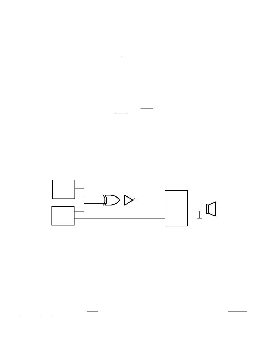
3≠10
3.6.7
Integrated Pullup Resistors for PC Card Interface
The PC Card Standard requires pullup resistors on various terminals to support both CardBus and 16-bit PC Card
configurations. The PCI7x20 device has integrated all of these pullup resistors and requires no additional external
components. The I/O buffer on the BVD1(STSCHG)/CSTSCHG terminal has the capability to switch to an internal
pullup resistor when a 16-bit PC Card is inserted, or switch to an internal pulldown resistor when a CardBus card is
inserted. This prevents inadvertent CSTSCHG events. The pullup resistor requirements for the various UltraMedia
interfaces are either included in the UltraMedia cards (or the UltraMedia adapter) or are part of the existing PCMCIA
architecture. The PCI7x20 device does not require any additional components for UltraMedia support.
3.6.8
SPKROUT and CAUDPWM Usage
The SPKROUT terminal carries the digital audio signal from the PC Card to the system. When a 16-bit PC Card is
configured for I/O mode, the BVD2 terminal becomes the SPKR input terminal from the card. This terminal, in
CardBus applications, is referred to as CAUDIO. SPKR passes a TTL-level binary audio signal to the PCI7x20 device.
The CardBus CAUDIO signal also can pass a single-amplitude binary waveform as well as a PWM signal. The binary
audio signal from each PC Card sockets is enabled by bit 1 (SPKROUTEN) of the card control register (PCI offset
91h, see Section 4.38).
Older controllers support CAUDIO in binary or PWM mode, but use the same output terminal (SPKROUT). Some
audio chips may not support both modes on one terminal and may have a separate terminal for binary and PWM.
The PCI7x20 implementation includes a signal for PWM, CAUDPWM, which can be routed to an MFUNC terminal.
Bit 2 (AUD2MUX), located in the card control register, is programmed to route a CardBus CAUDIO PWM terminal
to CAUDPWM. See Section 4.36, Multifunction Routing Register, for details on configuring the MFUNC terminals.
Figure 3≠4 illustrates the SPKROUT connection.
Speaker
Subsystem
BINARY_SPKR
System
Core Logic
PCI7x20
CAUDPWM
SPKROUT
PWM_SPKR
Figure 3≠4. SPKROUT Connection to Speaker Driver
3.6.9
LED Socket Activity Indicators
The socket activity LEDs are provided to indicate when a PC Card is being accessed. The LEDA1 and LEDA2 signals
can be routed to the multifunction terminals. When configured for LED outputs, these terminals output an active high
signal to indicate socket activity. LEDA1 indicates socket A (card A) activity, and LEDA2 indicates socket B (card B)
activity. The LED_SKT output indicates socket activity to either socket A or socket B. See Section 4.36, Multifunction
Routing Status Register,
for details on configuring the multifunction terminals.
The active-high LED signal is driven for 64 ms. When the LED is not being driven high, it is driven to a low state. Either
of the two circuits shown in Figure 3≠5 can be implemented to provide LED signaling, and the board designer must
implement the circuit that best fits the application.
The LED activity signals are valid when a card is inserted, powered, and not in reset. For PC Card-16, the LED activity
signals are pulsed when READY(IREQ) is low. For CardBus cards, the LED activity signals are pulsed if CFRAME,
IRDY, or CREQ are active.
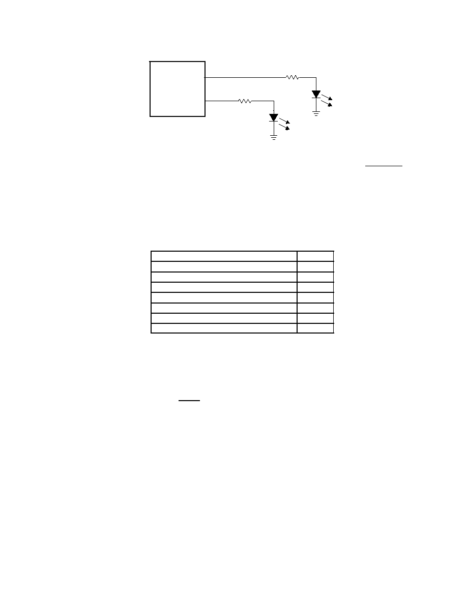
3≠11
PCI7x20
Current Limiting
R
150
Socket A
LED
MFUNCx
Current Limiting
R
150
MFUNCy
Socket B
LED
Figure 3≠5. Two Sample LED Circuits
As indicated, the LED signals are driven for a period of 64 ms by a counter circuit. To avoid the possibility of the LEDs
appearing to be stuck when the PCI clock is stopped, the LED signaling is cut off when the SUSPEND signal is
asserted, when the PCI clock is to be stopped during the clock run protocol, or when in the D2 or D1 power state.
If any additional socket activity occurs during this counter cycle, then the counter is reset and the LED signal remains
driven. If socket activity is frequent (at least once every 64 ms), then the LED signals remain driven.
3.6.10 CardBus Socket Registers
The PCI7x20 device contains all registers for compatibility with the PCI Local Bus Specification and the PC Card
Standard. These registers, which exist as the CardBus socket registers, are listed in Table 3≠7.
Table 3≠7. CardBus Socket Registers
REGISTER NAME
OFFSET
Socket event
00h
Socket mask
04h
Socket present state
08h
Socket force event
0Ch
Socket control
10h
Reserved
14h≠1Ch
Socket power management
20h
3.6.11 48-MHz Clock Requirements
The PCI7x20 device is designed to use an external 48-MHz clock connected to the CLK_48 terminal to provide the
reference for an internal oscillator circuit. This oscillator in turn drives a PLL circuit that generates the various clocks
required for the flash media function (Function 3) of the PCI7x20 device.
The 48-MHz clock must maintain a frequency of 48 MHz
±
0.8% over normal operating conditions. This clock must
maintain a duty cycle of 40% ≠ 60%. The PCI7x20 device requires that the 48-MHz clock be running and stable (a
minimum of 10 clock pulses) before a GRST deassertion.
The following are typical specifications for crystals used with the PCI7x20 device in order to achieve the required
frequency accuracy and stability.
∑
Crystal mode of operation: Fundamental
∑
Frequency tolerance @ 25
∞
C: Total frequency variation for the complete circuit is
±
100 ppm. A crystal with
±
30 ppm frequency tolerance is recommended for adequate margin.
∑
Frequency stability (over temperature and age): A crystal with
±
30 ppm frequency stability is recommended
for adequate margin.
NOTE: The total frequency variation must be kept below
±
100 ppm from nominal with some
allowance for error introduced by board and device variations. Trade-offs between frequency
tolerance and stability may be made as long as the total frequency variation is less than
±
100 ppm. For example, the frequency tolerance of the crystal may be specified at 50 ppm and
the temperature tolerance may be specified at 30 ppm to give a total of 80 ppm possible
variation due to the crystal alone. Crystal aging also contributes to the frequency variation.

3≠12
3.7
Serial EEPROM Interface
The PCI7x20 device has a dedicated serial bus interface that can be used with an EEPROM to load certain registers
in the PCI7x20 device. The EEPROM is detected by a pullup resistor on the SCL terminal. See Table 3≠9 for the
EEPROM loading map.
3.7.1
Serial-Bus Interface Implementation
The PCI7x20 device drives SCL at nearly 100 kHz during data transfers, which is the maximum specified frequency
for standard mode I
2
C. The serial EEPROM must be located at address A0h.
Some serial device applications may include PC Card power switches, card ejectors, or other devices that may
enhance the user's PC Card experience. The serial EEPROM device and PC Card power switches are discussed
in the sections that follow.
3.7.2
Accessing Serial-Bus Devices Through Software
The PCI7x20 device provides a programming mechanism to control serial bus devices through software. The
programming is accomplished through a doubleword of PCI configuration space at offset B0h. Table 3≠8 lists the
registers used to program a serial-bus device through software.
Table 3≠8. PCI7x20 Registers Used to Program Serial-Bus Devices
PCI OFFSET
REGISTER NAME
DESCRIPTION
B0h
Serial-bus data
Contains the data byte to send on write commands or the received data byte on read commands.
B1h
Serial-bus index
The content of this register is sent as the word address on byte writes or reads. This register is not used
in the quick command protocol.
B2h
Serial-bus slave
address
Write transactions to this register initiate a serial-bus transaction. The slave device address and the
R/W command selector are programmed through this register.
B3h
Serial-bus control
and status
Read data valid, general busy, and general error status are communicated through this register. In
addition, the protocol-select bit is programmed through this register.
3.7.3
Serial-Bus Interface Protocol
The SCL and SDA signals are bidirectional, open-drain signals and require pullup resistors as shown in Figure 3≠3.
The PCI7x20 device, which supports up to 100-Kb/s data-transfer rate, is compatible with standard mode I
2
C using
7-bit addressing.
All data transfers are initiated by the serial bus master. The beginning of a data transfer is indicated by a start
condition, which is signaled when the SDA line transitions to the low state while SCL is in the high state, as shown
in Figure 3≠6. The end of a requested data transfer is indicated by a stop condition, which is signaled by a low-to-high
transition of SDA while SCL is in the high state, as shown in Figure 3≠6. Data on SDA must remain stable during the
high state of the SCL signal, as changes on the SDA signal during the high state of SCL are interpreted as control
signals, that is, a start or a stop condition.
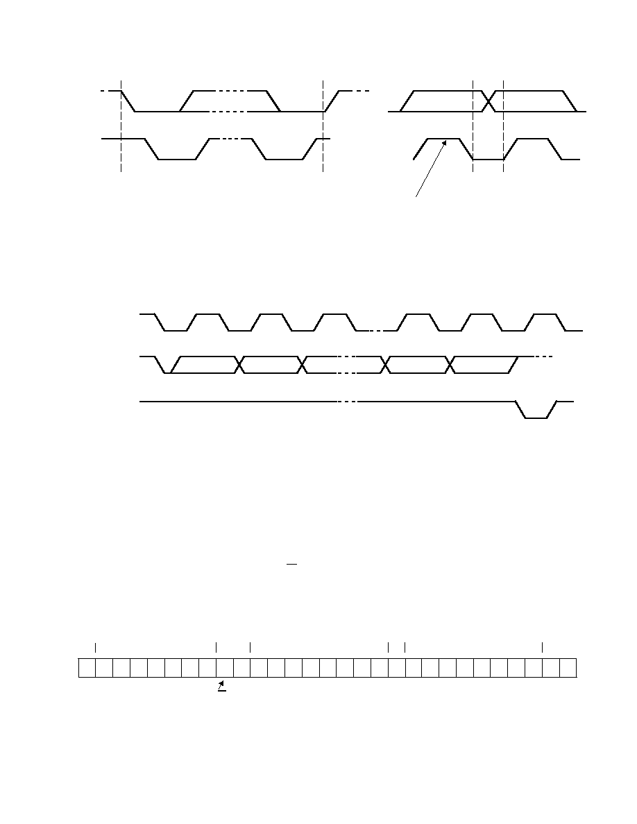
3≠13
SDA
SCL
Start
Condition
Stop
Condition
Change of
Data Allowed
Data Line Stable,
Data Valid
Figure 3≠6. Serial-Bus Start/Stop Conditions and Bit Transfers
Data is transferred serially in 8-bit bytes. The number of bytes that may be transmitted during a data transfer is
unlimited; however, each byte must be completed with an acknowledge bit. An acknowledge (ACK) is indicated by
the receiver pulling the SDA signal low, so that it remains low during the high state of the SCL signal. Figure 3≠7
illustrates the acknowledge protocol.
SCL From
Master
1
2
3
7
8
9
SDA Output
By Transmitter
SDA Output
By Receiver
Figure 3≠7. Serial-Bus Protocol Acknowledge
The PCI7x20 device is a serial bus master; all other devices connected to the serial bus external to the PCI7x20
device are slave devices. As the bus master, the PCI7x20 device drives the SCL clock at nearly 100 kHz during bus
cycles and places SCL in a high-impedance state (zero frequency) during idle states.
Typically, the PCI7x20 device masters byte reads and byte writes under software control. Doubleword reads are
performed by the serial EEPROM initialization circuitry upon a PCI reset and may not be generated under software
control. See Section 3.7.4, Serial-Bus EEPROM Application, for details on how the PCI7x20 device automatically
loads the subsystem identification and other register defaults through a serial-bus EEPROM.
Figure 3≠8 illustrates a byte write. The PCI7x20 device issues a start condition and sends the 7-bit slave device
address and the command bit zero. A 0 in the R/W command bit indicates that the data transfer is a write. The slave
device acknowledges if it recognizes the address. If no acknowledgment is received by the PCI7x20 device, then an
appropriate status bit is set in the serial-bus control/status register (PCI offset B3h, see Section 4.50). The word
address byte is then sent by the PCI7x20 device, and another slave acknowledgment is expected. Then the PCI7x20
device delivers the data byte MSB first and expects a final acknowledgment before issuing the stop condition.
S
b6
b4
b5
b3 b2 b1 b0
0
b7 b6 b5 b4 b3
b2 b1 b0
A
A
Slave Address
Word Address
R/W
S/P = Start/Stop Condition
A = Slave Acknowledgement
b7 b6
b4
b5
b3 b2 b1 b0
A
P
Data Byte
Figure 3≠8. Serial-Bus Protocol--Byte Write
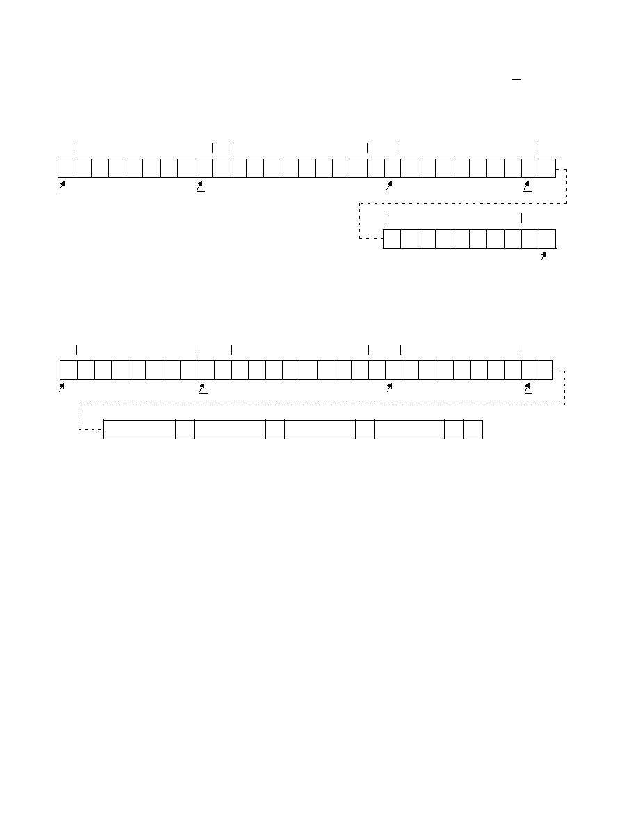
3≠14
Figure 3≠9 illustrates a byte read. The read protocol is very similar to the write protocol, except the R/W command
bit must be set to 1 to indicate a read-data transfer. In addition, the PCI7x20 master must acknowledge reception of
the read bytes from the slave transmitter. The slave transmitter drives the SDA signal during read data transfers. The
SCL signal remains driven by the PCI7x20 master.
S
b6
b4
b5
b3 b2 b1 b0
0
b7 b6 b5 b4 b3
b2 b1 b0
A
A
Slave Address
Word Address
R/W
S
b6
b4
b5
b3 b2 b1 b0
1
A
Slave Address
S/P = Start/Stop Condition
M = Master Acknowledgement
b7 b6
b4
b5
b3 b2 b1 b0
M
P
Data Byte
Start
Restart
R/W
A = Slave Acknowledgement
Stop
Figure 3≠9. Serial-Bus Protocol--Byte Read
Figure 3≠10 illustrates EEPROM interface doubleword data collection protocol.
S
1
1
0
0
0
0
0
0
b7 b6 b5 b4 b3
b2 b1 b0
A
A
Slave Address
Word Address
R/W
Data Byte 2
Data Byte 1
Data Byte 0
M
P
M
M
M = Master Acknowledgement
S/P = Start/Stop Condition
A = Slave Acknowledgement
Data Byte 3
M
S
1
1
0
0
0
0
0
1
A
Restart
R/W
Slave Address
Start
Figure 3≠10. EEPROM Interface Doubleword Data Collection
3.7.4
Serial-Bus EEPROM Application
When the PCI bus is reset and the serial-bus interface is detected, the PCI7x20 device attempts to read the
subsystem identification and other register defaults from a serial EEPROM.
This format must be followed for the PCI7x20 device to load initializations from a serial EEPROM. All bit fields must
be considered when programming the EEPROM.
The serial EEPROM is addressed at slave address 1010 000b by the PCI7x20 device. All hardware address bits for
the EEPROM must be tied to the appropriate level to achieve this address. The serial EEPROM chip in the sample
application (Figure 3≠10) assumes the 1010b high-address nibble. The lower three address bits are terminal inputs
to the chip, and the sample application shows these terminal inputs tied to GND.

3≠15
Table 3≠9. EEPROM Loading Map
SERIAL ROM
OFFSET
BYTE DESCRIPTION
00h
CardBus function indicator (00h)
01h
Number of bytes (20h)
02h
PCI 04h, command register, function 0, bits 8, 6≠5, 2≠0
02h
[7]
Command
register, bit 8
[6]
Command
register, bit 6
[5]
Command
register, bit 5
[4:3]
RSVD
[2]
Command
register, bit 2
[1]
Command
register, bit 1
[0]
Command
register, bit 0
03h
PCI 04h, command register, function 1, bits 8, 6≠5, 2≠0
03h
[7]
Command
register, bit 8
[6]
Command
register, bit 6
[5]
Command
register, bit 5
[4:3]
RSVD
[2]
Command
register, bit 2
[1]
Command
register, bit 1
[0]
Command
register, bit 0
04h
PCI 40h, subsystem vendor ID, byte 0
05h
PCI 41h, subsystem vendor ID, byte 1
06h
PCI 42h, subsystem ID, byte 0
07h
PCI 43h, subsystem ID, byte 1
08h
PCI 44h, PC Card 16-bit I/F legacy mode base address register, byte 0, bits 7≠1
09h
PCI 45h, PC Card 16-bit I/F legacy mode base address register, byte 1
0Ah
PCI 46h, PC Card 16-bit I/F legacy mode base address register, byte 2
0Bh
PCI 47h, PC Card 16-bit I/F legacy mode base address register, byte 3
0Ch
PCI 80h, system control, function 0, byte 0, bits 6≠0
0Dh
PCI 80h, system control, function 1, byte 0, bit 2
0Eh
PCI 81h, system control, byte 1
0Fh
Reserved load all 0s (PCI 82h, system control, byte 2)
10h
PCI 83h, system control, byte 3
11h
PCI 8Ch, MFUNC routing, byte 0
12h
PCI 8Dh, MFUNC routing, byte 1
13h
PCI 8Eh, MFUNC routing, byte 2
14h
PCI 8Fh, MFUNC routing, byte 3
15h
PCI 90h, retry status, bits 7, 6
16h
PCI 91h, card control, bit 7
17h
PCI 92h, device control, bits 6, 5, 3≠0
18h
PCI 93h, diagnostic, bits 7, 4≠0
19h
PCI A2h, power-management capabilities, function 0, bit 15 (bit 7 of EEPROM offset 16h corresponds to bit 15)
1Ah
PCI A2h, power-management capabilities, function 1, bit 15 (bit 7 of EEPROM offset 16h corresponds to bit 15)
1Bh
CB Socket + 0Ch, function 0 socket force event, bit 27 (bit 3 of EEPROM offset 17h corresponds to bit 27)
1Ch
CB Socket + 0Ch, function 1 socket force event, bit 27 (bit 3 of EEPROM offset 18h corresponds to bit 27)
1Dh
ExCA 00h, ExCA identification and revision, bits 7≠0
1Eh
PCI 86h, general control, byte 0, bits 5, 4, 3, 1, 0
1Fh
PCI 87h, general control, byte 1, bits 4≠2
20h
PCI 89h, GPE enable, bits 7, 6, 4≠0
21h
PCI 8Bh, general-purpose output, bits 4≠0
22h
1394 OHCI function indicator (02h)
23h
Number of bytes (17h)
24h
PCI 3Fh, maximum latency bits 7≠4
PCI 3Eh, minimum grant, bits 3≠0
25h
PCI 2Ch, subsystem vendor ID, byte 0

3≠16
Table 3≠9. EEPROM Loading Map (Continued)
SERIAL ROM
OFFSET
BYTE DESCRIPTION
26h
PCI 2Dh, subsystem vendor ID, byte 1
27h
PCI 2Eh, subsystem ID, byte 0
28h
PCI 2Fh, subsystem ID, byte 1
29h
PCI F4h, Link_Enh, byte 0, bits 7, 2, 1
OHCI 50h, host controller control, bit 23
[7]
Link_Enh.
enab_unfair
[6]
HCControl.Program Phy Enable
[5:3]
RSVD
[2]
Link_Enh, bit 2
[1]
Link_Enh.
enab_accel
[0]
RSVD
2Ah
Mini-ROM address, this byte indicates the MINI ROM offset into the EEPROM
00h = No MINI ROM
Other Values = MINI ROM offset
2Bh
OHCI 24h, GUIDHi, byte 0
2Ch
OHCI 25h, GUIDHi, byte 1
2Dh
OHCI 26h, GUIDHi, byte 2
2Eh
OHCI 27h, GUIDHi, byte 3
2Fh
OHCI 28h, GUIDLo, byte 0
30h
OHCI 29h, GUIDLo, byte 1
31h
OHCI 2Ah, GUIDLo, byte 2
32h
OHCI 2Bh, GUIDLo, byte 3
33h
Checksum (Reserved--no bit loaded)
34h
PCI F5h, Link_Enh, byte 1, bits 7, 6, 5, 4
35h
PCI F0h, PCI miscellaneous, byte 0, bits 5, 4, 2, 1, 0
36h
PCI F1h, PCI miscellaneous, byte 1, bits 7, 3, 2, 1, 0
37h
Reserved
38h
Reserved (CardBus CIS pointer)
39h
Reserved
3Ah
PCI ECh, PCI PHY control, bits 7, 3, 1
3Bh
Flash media core function indicator (03h)
3Ch
Number of bytes (05h)
3Dh
PCI 2Ch, subsystem vendor ID, byte 0
3Eh
PCI 2Dh, subsystem vendor ID, byte 1
3Fh
PCI 2Eh, subsystem ID, byte 0
40h
PCI 2Fh, subsystem ID, byte 1
41h
PCI 4Ch, general control, bits 6≠0
42h
End-of-list indicator (80h)
3.8
Programmable Interrupt Subsystem
Interrupts provide a way for I/O devices to let the microprocessor know that they require servicing. The dynamic
nature of PC Cards and the abundance of PC Card I/O applications require substantial interrupt support from the
PCI7x20 device. The PCI7x20 device provides several interrupt signaling schemes to accommodate the needs of
a variety of platforms. The different mechanisms for dealing with interrupts in this device are based on various
specifications and industry standards. The ExCA register set provides interrupt control for some 16-bit PC Card
functions, and the CardBus socket register set provides interrupt control for the CardBus PC Card functions. The
PCI7x20 device is, therefore, backward compatible with existing interrupt control register definitions, and new
registers have been defined where required.

3≠17
The PCI7x20 device detects PC Card interrupts and events at the PC Card interface and notifies the host controller
using one of several interrupt signaling protocols. To simplify the discussion of interrupts in the PCI7x20 device, PC
Card interrupts are classified either as card status change (CSC) or as functional interrupts.
The method by which any type of PCI7x20 interrupt is communicated to the host interrupt controller varies from
system to system. The PCI7x20 device offers system designers the choice of using parallel PCI interrupt signaling,
parallel ISA-type IRQ interrupt signaling, or the IRQSER serialized ISA and/or PCI interrupt protocol. It is possible
to use the parallel PCI interrupts in combination with either parallel IRQs or serialized IRQs, as detailed in the sections
that follow. All interrupt signaling is provided through the seven multifunction terminals, MFUNC0≠MFUNC6.
3.8.1
PC Card Functional and Card Status Change Interrupts
PC Card functional interrupts are defined as requests from a PC Card application for interrupt service and are
indicated by asserting specially-defined signals on the PC Card interface. Functional interrupts are generated by
16-bit I/O PC Cards and by CardBus PC Cards.
Card status change (CSC)-type interrupts are defined as events at the PC Card interface that are detected by the
PCI7x20 device and may warrant notification of host card and socket services software for service. CSC events
include both card insertion and removal from PC Card sockets, as well as transitions of certain PC Card signals.
Table 3≠10 summarizes the sources of PC Card interrupts and the type of card associated with them. CSC and
functional interrupt sources are dependent on the type of card inserted in the PC Card socket. The four types of cards
that can be inserted into any PC Card socket are:
∑
16-bit memory card
∑
16-bit I/O card
∑
CardBus cards
∑
UltraMedia card
Table 3≠10. Interrupt Mask and Flag Registers
CARD TYPE
EVENT
MASK
FLAG
16 bit memory
Battery conditions (BVD1, BVD2)
ExCA offset 05h/45h/805h bits 1 and 0
ExCA offset 04h/44h/804h bits 1 and 0
16-bit memory
Wait states (READY)
ExCA offset 05h/45h/805h bit 2
ExCA offset 04h/44h/804h bit 2
16-bit I/O
Change in card status (STSCHG)
ExCA offset 05h/45h/805h bit 0
ExCA offset 04h/44h/804h bit 0
16-bit I/O/
UltraMedia
Interrupt request (IREQ)
Always enabled
PCI configuration offset 91h bit 0
All 16-bit PC
Cards/
Smart Card
adapters/
UltraMedia/
Flash Media
Power cycle complete
ExCA offset 05h/45h/805h bit 3
ExCA offset 04h/44h/804h bit 3
Change in card status (CSTSCHG)
Socket mask bit 0
Socket event bit 0
CardBus
Interrupt request (CINT)
Always enabled
PCI configuration offset 91h bit 0
CardBus
Power cycle complete
Socket mask bit 3
Socket event bit 3
Card insertion or removal
Socket mask bits 2 and 1
Socket event bits 2 and 1
Functional interrupt events are valid only for 16-bit I/O and CardBus cards; that is, the functional interrupts are not
valid for 16-bit memory cards. Furthermore, card insertion and removal-type CSC interrupts are independent of the
card type.
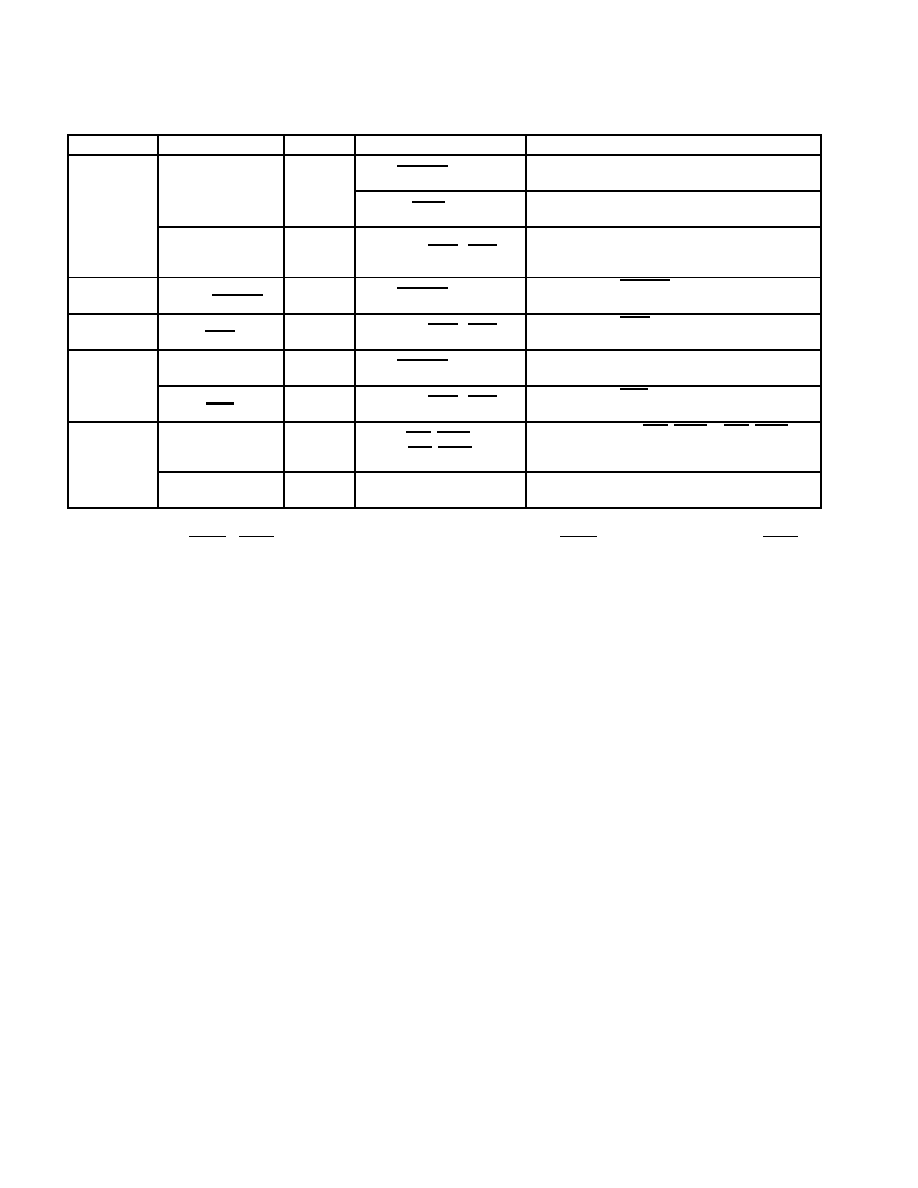
3≠18
Table 3≠11. PC Card Interrupt Events and Description
CARD TYPE
EVENT
TYPE
SIGNAL
DESCRIPTION
Battery conditions
CSC
BVD1(STSCHG)//CSTSCHG
A transition on BVD1 indicates a change in the
PC Card battery conditions.
16-bit
memory
Battery conditions
(BVD1, BVD2)
CSC
BVD2(SPKR)//CAUDIO
A transition on BVD2 indicates a change in the
PC Card battery conditions.
memory
Wait states
(READY)
CSC
READY(IREQ)//CINT
A transition on READY indicates a change in the
ability of the memory PC Card to accept or provide
data.
16-bit I/O
Change in card
status (STSCHG)
CSC
BVD1(STSCHG)//CSTSCHG
The assertion of STSCHG indicates a status change
on the PC Card.
16-bit I/O/
UltraMedia
Interrupt request
(IREQ)
Functional
READY(IREQ)//CINT
The assertion of IREQ indicates an interrupt request
from the PC Card.
CardBus
Change in card
status (CSTSCHG)
CSC
BVD1(STSCHG)//CSTSCHG
The assertion of CSTSCHG indicates a status
change on the PC Card.
CardBus
Interrupt request
(CINT)
Functional
READY(IREQ)//CINT
The assertion of CINT indicates an interrupt request
from the PC Card.
All PC Cards/
Smart Card
adapters/
Card insertion
or removal
CSC
CD1//CCD1,
CD2//CCD2
A transition on either CD1//CCD1 or CD2//CCD2
indicates an insertion or removal of a 16-bit or
CardBus PC Card.
ada ters/
UltraMedia/
Flash Media
Power cycle
complete
CSC
N/A
An interrupt is generated when a PC Card power-up
cycle has completed.
The naming convention for PC Card signals describes the function for 16-bit memory, I/O cards, and CardBus. For
example, READY(IREQ)//CINT includes READY for 16-bit memory cards, IREQ for 16-bit I/O cards, and CINT for
CardBus cards. The 16-bit memory card signal name is first, with the I/O card signal name second, enclosed in
parentheses. The CardBus signal name follows after a double slash (//).
The 1997 PC Card Standard describes the power-up sequence that must be followed by the PCI7x20 device when
an insertion event occurs and the host requests that the socket V
CC
and V
PP
be powered. Upon completion of this
power-up sequence, the PCI7x20 interrupt scheme can be used to notify the host system (see Table 3≠11), denoted
by the power cycle complete event. This interrupt source is considered a PCI7x20 internal event, because it depends
on the completion of applying power to the socket rather than on a signal change at the PC Card interface.
3.8.2
Interrupt Masks and Flags
Host software may individually mask (or disable) most of the potential interrupt sources listed in Table 3≠11 by setting
the appropriate bits in the PCI7x20 device. By individually masking the interrupt sources listed, software can control
those events that cause a PCI7x20 interrupt. Host software has some control over the system interrupt the PCI7x20
device asserts by programming the appropriate routing registers. The PCI7x20 device allows host software to route
PC Card CSC and PC Card functional interrupts to separate system interrupts. Interrupt routing somewhat specific
to the interrupt signaling method used is discussed in more detail in the following sections.
When an interrupt is signaled by the PCI7x20 device, the interrupt service routine must determine which of the events
listed in Table 3≠10 caused the interrupt. Internal registers in the PCI7x20 device provide flags that report the source
of an interrupt. By reading these status bits, the interrupt service routine can determine the action to be taken.
Table 3≠10 details the registers and bits associated with masking and reporting potential interrupts. All interrupts can
be masked except the functional PC Card interrupts, and an interrupt status flag is available for all types of interrupts.
Notice that there is not a mask bit to stop the PCI7x20 device from passing PC Card functional interrupts through to
the appropriate interrupt scheme. These interrupts are not valid until the card is properly powered, and there must
never be a card interrupt that does not require service after proper initialization.
Table 3≠10 lists the various methods of clearing the interrupt flag bits. The flag bits in the ExCA registers (16-bit PC
Card-related interrupt flags) can be cleared using two different methods. One method is an explicit write of 1 to the
flag bit to clear and the other is by reading the flag bit register. The selection of flag bit clearing methods is made by

3≠19
bit 2 (IFCMODE) in the ExCA global control register (ExCA offset 1Eh/5Eh/81Eh, see Section 5.20), and defaults to
the flag-cleared-on-read method.
The CardBus-related interrupt flags can be cleared by an explicit write of 1 to the interrupt flag in the socket event
register (see Section 6.1). Although some of the functionality is shared between the CardBus registers and the ExCA
registers, software must not program the chip through both register sets when a CardBus card is functioning.
3.8.3
Using Parallel IRQ Interrupts
The seven multifunction terminals, MFUNC6≠MFUNC0, implemented in the PCI7x20 device can be routed to obtain
a subset of the ISA IRQs. The IRQ choices provide ultimate flexibility in PC Card host interruptions. To use the parallel
ISA-type IRQ interrupt signaling, software must program the device control register (PCI offset 92h, see
Section 4.39), to select the parallel IRQ signaling scheme. See Section 4.36, Multifunction Routing Status Register,
for details on configuring the multifunction terminals.
A system using parallel IRQs requires (at a minimum) one PCI terminal, INTA, to signal CSC events. This requirement
is dictated by certain card and socket-services software. The INTA requirement calls for routing the MFUNC0 terminal
for INTA signaling. The INTRTIE bit is used, in this case, to route socket interrupt events to INTA. This leaves (at a
maximum) six different IRQs to support legacy 16-bit PC Card functions.
As an example, suppose the six IRQs used by legacy PC Card applications are IRQ3, IRQ4, IRQ5, IRQ10, IRQ11,
and IRQ15. The multifunction routing status register must be programmed to a value of 0FBA 5432h. This value
routes the MFUNC0 terminal to INTA signaling and routes the remaining terminals as illustrated in Figure 3≠11. Not
shown is that INTA must also be routed to the programmable interrupt controller (PIC), or to some circuitry that
provides parallel PCI interrupts to the host.
PCI7x20
PIC
MFUNC1
MFUNC2
MFUNC3
MFUNC4
MFUNC5
MFUNC6
IRQ3
IRQ4
IRQ5
IRQ11
IRQ10
IRQ15
Figure 3≠11. IRQ Implementation
Power-on software is responsible for programming the multifunction routing status register to reflect the IRQ
configuration of a system implementing the PCI7x20 device. The multifunction routing status register is a global
register that is shared between the four PCI7x20 functions. See Section 4.36, Multifunction Routing Status Register,
for details on configuring the multifunction terminals.
The parallel ISA-type IRQ signaling from the MFUNC6≠MFUNC0 terminals is compatible with the input signal
requirements of the 8259 PIC. The parallel IRQ option is provided for system designs that require legacy ISA IRQs.
Design constraints may demand more MFUNC6≠MFUNC0 IRQ terminals than the PCI7x20 device makes available.
3.8.4
Using Parallel PCI Interrupts
Parallel PCI interrupts are available when exclusively in parallel PCI interrupt/parallel ISA IRQ signaling mode, and
when only IRQs are serialized with the IRQSER protocol. The INTA, INTB, INTC, and INTD can be routed to MFUNC
terminals (MFUNC0, MFUNC1, MFUNC2, and MFUNC4). If bit 29 (INTRTIE) is set in the system control register (PCI
offset 80h, see Section 4.29), then INTA and INTB are tied internally. When the TIEALL bit is set, all four functions
return a value of 01h on reads from the interrupt pin register for both parallel and serial PCI interrupts.
The INTRTIE and TIEALL bits affect the read-only value provided through accesses to the interrupt pin register (PCI
offset 3Dh, see Section 4.24). Table 3≠12 summarizes the interrupt signaling modes.

3≠20
Table 3≠12. Interrupt Pin Register Cross Reference
INTRTIE Bit
TIEALL Bit
INTPIN
Function 0
(CardBus)
INTPIN
Function 1
(CardBus)
INTPIN
Function 2
(1394 OHCI)
INTPIN
Function 3
(Flash Media)
0
0
0x01 (INTA)
0x02 (INTB)
0x03 (INTC)
Determined by bits 6≠5 (INT_SEL
field) in flash media general control
1
0
0x01 (INTA)
0x01 (INTA)
0x03 (INTC)
field) in flash media general control
register (see Section 11.21)
X
1
0x01 (INTA)
0x01 (INTA)
0x01 (INTA)
0x01 (INTA)
3.8.5
Using Serialized IRQSER Interrupts
The serialized interrupt protocol implemented in the PCI7x20 device uses a single terminal to communicate all
interrupt status information to the host controller. The protocol defines a serial packet consisting of a start cycle,
multiple interrupt indication cycles, and a stop cycle. All data in the packet is synchronous with the PCI clock. The
packet data describes 16 parallel ISA IRQ signals and the optional 4 PCI interrupts INTA, INTB, INTC, and INTD. For
details on the IRQSER protocol, refer to the document Serialized IRQ Support for PCI Systems.
3.8.6
SMI Support in the PCI7x20 Device
The PCI7x20 device provides a mechanism for interrupting the system when power changes have been made to the
PC Card socket interfaces. The interrupt mechanism is designed to fit into a system maintenance interrupt (SMI)
scheme. SMI interrupts are generated by the PCI7x20 device, when enabled, after a write cycle to either the socket
control register (CB offset 10h, see Section 6.5) of the CardBus register set, or the ExCA power control register (ExCA
offset 02h/42h/802h, see Section 5.3) causes a power cycle change sequence to be sent on the power switch
interface.
The SMI control is programmed through three bits in the system control register (PCI offset 80h, see Section 4.29).
These bits are SMIROUTE (bit 26), SMISTATUS (bit 25), and SMIENB (bit 24). Table 3≠13 describes the SMI control
bits function.
Table 3≠13. SMI Control
BIT NAME
FUNCTION
SMIROUTE
This shared bit controls whether the SMI interrupts are sent as a CSC interrupt or as IRQ2.
SMISTAT
This socket-dependent bit is set when an SMI interrupt is pending. This status flag is cleared by writing back a 1.
SMIENB
When set, SMI interrupt generation is enabled. This bit is shared by functions 0 and 1.
If CSC SMI interrupts are selected, then the SMI interrupt is sent as the CSC on a per-socket basis. The CSC interrupt
can be either level or edge mode, depending upon the CSCMODE bit in the ExCA global control register (ExCA offset
1Eh/5Eh/81Eh, see Section 5.20).
If IRQ2 is selected by SMIROUTE, then the IRQSER signaling protocol supports SMI signaling in the IRQ2 IRQ/Data
slot. In a parallel ISA IRQ system, the support for an active low IRQ2 is provided only if IRQ2 is routed to either
MFUNC3 or MFUNC6 through the multifunction routing status register (PCI offset 8Ch, see Section 4.36).
3.9
Power Management Overview
In addition to the low-power CMOS technology process used for the PCI7x20 device, various features are designed
into the device to allow implementation of popular power-saving techniques. These features and techniques are as
follows:
∑
Clock run protocol
∑
Cardbus PC Card power management
∑
16-bit PC Card power management
∑
Suspend mode
∑
Ring indicate
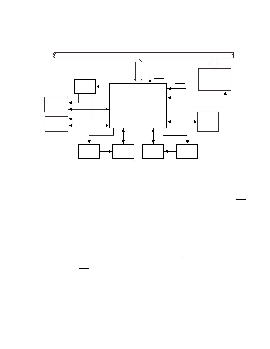
3≠21
∑
PCI power management
∑
Cardbus bridge power management
∑
ACPI support
PC Card/
Smart Card
Socket A
PCI Bus
PRST
GRST
Core Logic/
Embedded
Controller
1394
Sockets
PCI7x20
Power
Switch
MMC/SD
Power
Switch
MS/
MS PRO
Power
Switch
PC Card/
Smart Card
Socket B
The system connection to GRST is implementation-specific. GRST must be asserted on initial power up of the PCI7x20 device. PRST must be
asserted for subsequent warm resets.
Figure 3≠12. System Diagram Implementing CardBus Device Class Power Management
3.9.1
1394 Power Management (Function 2)
The PCI7x20 device complies with PCI Bus Power Management Interface Specification. The device supports the D0
(uninitialized), D0 (active), D1, D2, and D3 power states as defined by the power-management definition in the 1394
Open Host Controller Interface Specification, Appendix A.4 and PCI Bus Power Management Specification. PME is
supported to provide notification of wake events. Per Section A.4.2, the 1394 OHCI sets PMCSR.PME_STS in the
D0 state due to unmasked interrupt events. In previous OHCI implementations, unmasked interrupt events were
interpreted as (IntEvent.n && IntMask.n && IntMask.masterIntEnable), where n represents a specific interrupt event.
Based on feedback from Microsoft this implementation may cause problems with the existing Windows
power-management arcitecture as a PME and an interrupt could be simultaneously signaled on a transition from the
D1 to D0 state where interrupts were enabled to generate wake events. If bit 10 (ignore_mstrIntEna_for_pme) in the
PCI miscellaneous configuration register (OHCI offset F0h, see Section 7.22) is set, then the PCI7x20 device
implements the preferred behavior as (IntEvent.n && IntMask.n). Otherwise, the PCI7x20 device implements the
preferred behavior as (IntEvent.n && IntMask.n && IntMask.masterIntEnable). In addition, when the
ignore_mstrIntEna_for_pme bit is set, it causes bit 26 of the OHCI vendor ID register (OHCI offset 40h, see
Section 8.15) to read 1, otherwise, bit 26 reads 0. An open drain buffer is used for PME. If PME is enabled in the power
management control/status register (PCI offset A4h, see Section 4.44), then insertion of a PC Card causes the
PCI7x20 device to assert PME, which wakes the system from a low power state (D3, D2, or D1). The OS services
PME and takes the PCI7x20 device to the D0 state.
3.9.2
Integrated Low-Dropout Voltage Regulator (LDO-VR)
The PCI7x20 device requires 1.8-V core voltage. The core power can be supplied by the PCI7x20 device itself using
the internal
LDO-VR. The core power can alternatively be supplied by an external power supply through the
VR_PORT terminal. Table 3≠14 lists the requirements for both the internal core power supply and the external core
power supply.

3≠22
Table 3≠14. Requirements for Internal/External 1.8-V Core Power Supply
SUPPLY
VCC
VR_EN
VR_PORT
NOTE
Internal
3.3 V
GND
1.8-V output
Internal 1.8-V LDO-VR is enabled. A 1.0-
µ
F bypass capacitor is required on the VR_PORT
terminal for decoupling. This output is not for external use.
External
3.3 V
VCC
1.8-V input
Internal 1.8-V LDO-VR is disabled. An external 1.8-V power supply, of minimum 50-mA
capacity, is required. A 0.1-
µ
F bypass capacitor on the VR_PORT terminal is required.
3.9.3
CardBus (Functions 0 and 1) Clock Run Protocol
The PCI CLKRUN feature is the primary method of power management on the PCI interface of the PCI7x20 device.
CLKRUN signaling is provided through the MFUNC6 terminal. Since some chip sets do not implement CLKRUN, this
is not always available to the system designer, and alternate power-saving features are provided. For details on the
CLKRUN protocol see the PCI Mobile Design Guide.
The PCI7x20 device does not permit the central resource to stop the PCI clock under any of the following conditions:
∑
Bit 1 (KEEPCLK) in the system control register (PCI offset 80h, see Section 4.29) is set.
∑
The 16-bit PC Card resource manager is busy.
∑
The PCI7x20 CardBus master state machine is busy. A cycle may be in progress on CardBus.
∑
The PCI7x20 master is busy. There may be posted data from CardBus to PCI in the PCI7x20 device.
∑
Interrupts are pending.
∑
The CardBus CCLK for the socket has not been stopped by the PCI7x20 CCLKRUN manager.
∑
Bit 0 (KEEP_PCLK) in the miscellaneous configuration register (PCI offset F0h, see Section 7.22) is set.
∑
The 1394 resource manager is busy.
∑
The PCI7x20 1394 master state machine is busy. A cycle may be in progress on 1394.
∑
The PCI7x20 master is busy. There may be posted data from the 1394 bus to PCI in the PCI7x20 device.
∑
Interrupts are pending.
∑
The 1394 bus is not idle.
The PCI7x20 device restarts the PCI clock using the CLKRUN protocol under any of the following conditions:
∑
A 16-bit PC Card IREQ or a CardBus CINT has been asserted by either card.
∑
A CardBus CBWAKE (CSTSCHG) or 16-bit PC Card STSCHG/RI event occurs in the socket.
∑
A CardBus attempts to start the CCLK using CCLKRUN.
∑
A CardBus card arbitrates for the CardBus bus using CREQ.
∑
A 1394 device changes the status of the twisted pair lines from idle to active.
∑
Bit 1 (KEEPCLK) in the system control register (PCI offset 80h, see Section 4.29) is set.
∑
Data is in any of the FIFOs (receive or transmit).
∑
The master state machine is busy.
∑
There are pending interrupts.
3.9.4
CardBus PC Card Power Management
The PCI7x20 device implements its own card power-management engine that can turn off the CCLK to a socket when
there is no activity to the CardBus PC Card. The PCI clock-run protocol is followed on the CardBus CCLKRUN
interface to control this clock management.
3.9.5
16-Bit PC Card Power Management
The COE bit (bit 7) of the ExCA power control register (ExCA offset 02h/42h/802h, see Section 5.3) and PWRDWN
bit (bit 0) of the ExCA global control register (ExCA offset 1Eh/5Eh/81Eh, see Section 5.20) are provided for 16-bit
PC Card power management. The COE bit places the card interface in a high-impedance state to save power. The
power savings when using this feature are minimal. The COE bit resets the PC Card when used, and the PWRDWN
bit does not. Furthermore, the PWRDWN bit is an automatic COE, that is, the PWRDWN performs the COE function
when there is no card activity.
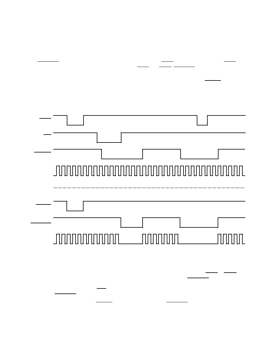
3≠23
NOTE: The 16-bit PC Card must implement the proper pullup resistors for the COE and
PWRDWN modes.
3.9.6
Suspend Mode
The SUSPEND signal, provided for backward compatibility, gates the PRST (PCI reset) signal and the GRST (global
reset) signal from the PCI7x20 device. Besides gating PRST and GRST, SUSPEND also gates PCLK inside the
PCI7x20 device in order to minimize power consumption.
It should also be noted that asynchronous signals, such as card status change interrupts and RI_OUT, can be passed
to the host system without a PCI clock. However, if card status change interrupts are routed over the serial interrupt
stream, then the PCI clock must be restarted in order to pass the interrupt, because neither the internal oscillator nor
an external clock is routed to the serial-interrupt state machine. Figure 3≠13 is a signal diagram of the suspend
function.
RESET
GNT
SUSPEND
PCLK
RESETIN
SUSPENDIN
PCLKIN
External Terminals
Internal Signals
Figure 3≠13. Signal Diagram of Suspend Function
3.9.7
Requirements for Suspend Mode
The suspend mode prevents the clearing of all register contents on the assertion of reset (PRST or GRST) which
would require the reconfiguration of the PCI7x20 device by software. Asserting the SUSPEND signal places the PCI
outputs of the controller in a high-impedance state and gates the PCLK signal internally to the controller unless a PCI
transaction is currently in process (GNT is asserted). It is important that the PCI bus not be parked on the PCI7x20
device when SUSPEND is asserted because the outputs are in a high-impedance state.
The GPIOs, MFUNC signals, and RI_OUT signal are all active during SUSPEND, unless they are disabled in the
appropriate PCI7x20 registers.
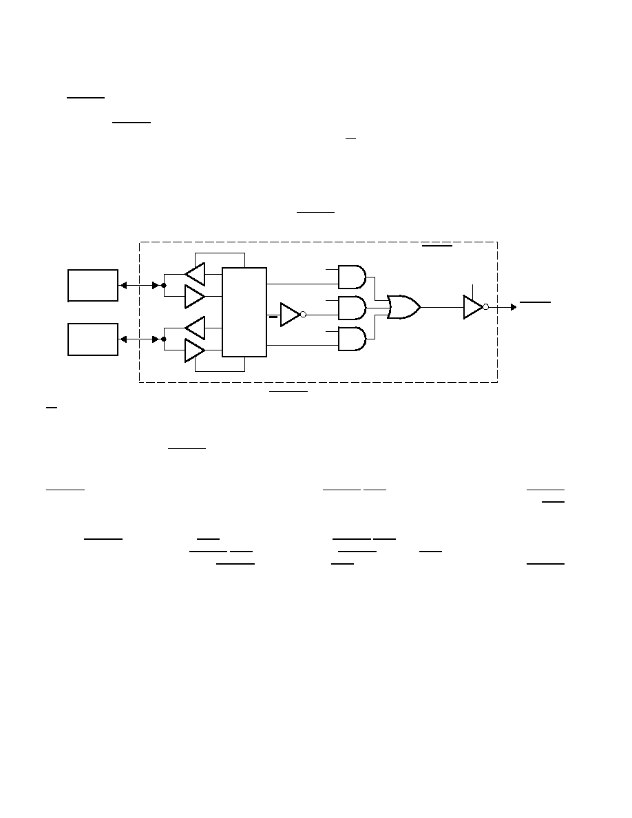
3≠24
3.9.8
Ring Indicate
The RI_OUT output is an important feature in power management, allowing a system to go into a suspended mode
and wake-up on modem rings and other card events. TI-designed flexibility permits this signal to fit wide platform
requirements. RI_OUT on the PCI7x20 device can be asserted under any of the following conditions:
∑
A 16-bit PC Card modem in a powered socket asserts RI to indicate to the system the presence of an
incoming call.
∑
A powered down CardBus card asserts CSTSCHG (CBWAKE) requesting system and interface wake-up.
∑
A powered CardBus card asserts CSTSCHG from the insertion/removal of cards or change in battery
voltage levels.
Figure 3≠14 shows various enable bits for the PCI7x20 RI_OUT function; however, it does not show the masking of
CSC events. See Table 3≠10 for a detailed description of CSC interrupt masks and flags.
Card
I/F
PC Card
Socket A
CSC
CSTSMASK
RIENB
RI_OUT
RI_OUT Function
RINGEN
CDRESUME
CSC
RI
PC Card
Socket B
Figure 3≠14. RI_OUT Functional Diagram
RI from the 16-bit PC Card interface is masked by bit 7 (RINGEN) in the ExCA interrupt and general control register
(ExCA offset 03h/43h/803h, see Section 5.4). This is programmed on a per-socket basis and is only applicable when
a 16-bit card is powered in the socket.
The CBWAKE signaling to RI_OUT is enabled through the same mask as the CSC event for CSTSCHG. The mask
bit (bit 0, CSTSMASK) is programmed through the socket mask register (CB offset 04h, see Section 6.2) in the
CardBus socket registers.
RI_OUT can be routed through any of three different pins, RI_OUT/PME, MFUNC2, or MFUNC4. The RI_OUT
function is enabled by setting bit 7 (RIENB) in the card control register (PCI offset 91h, see Section 4.38). The PME
function is enabled by setting bit 8 (PME_ENABLE) in the power-management control/status register (PCI offset A4h,
see Section 4.44). When bit 0 (RIMUX) in the system control register (PCI offset 80h, see Section 4.29) is set to 0,
both the RI_OUT function and the PME function are routed to the RI_OUT/PME terminal. If both functions are enabled
and RIMUX is set to 0, then the RI_OUT/PME terminal becomes RI_OUT only and PME assertions are never seen.
Therefore, in a system using both the RI_OUT function and the PME function, RIMUX must be set to 1 and RI_OUT
must be routed to either MFUNC2 or MFUNC4.
3.9.9
PCI Power Management
3.9.9.1 CardBus Power Management (Functions 0 and 1)
The PCI Bus Power Management Interface Specification for PCI to CardBus Bridges establishes the infrastructure
required to let the operating system control the power of PCI functions. This is done by defining a standard PCI
interface and operations to manage the power of PCI functions on the bus. The PCI bus and the PCI functions can
be assigned one of seven power-management states, resulting in varying levels of power savings.
The seven power-management states of PCI functions are:
∑
D0-uninitialized ≠ Before device configuration, device not fully functional
∑
D0-active ≠ Fully functional state

3≠25
∑
D1 ≠ Low-power state
∑
D2 ≠ Low-power state
∑
D3
hot
≠ Low-power state. Transition state before D3
cold
∑
D3
cold
≠ PME signal-generation capable. Main power is removed and VAUX is available.
∑
D3
off
≠ No power and completely nonfunctional
NOTE 1: In the D0-uninitialized state, the PCI7x20 device does not generate PME and/or interrupts. When bits 0 (IO_EN) and 1 (MEM_EN) of
the command register (PCI offset 04h, see Section 4.4) are both set, the PCI7x20 device switches the state to D0-active. Transition
from D3cold to the D0-uninitialized state happens at the deassertion of PRST. The assertion of GRST forces the controller to the
D0-uninitialized state immediately.
NOTE 2: The PWR_STATE bits (bits 1≠0) of the power-management control/status register (PCI offset A4h, see Section 4.44) only code for four
power states, D0, D1, D2, and D3hot. The differences between the three D3 states is invisible to the software because the controller
is not accessible in the D3cold or D3off state.
Similarly, bus power states of the PCI bus are B0≠B3. The bus power states B0≠B3 are derived from the device power
state of the originating bridge device.
For the operating system (OS) to manage the device power states on the PCI bus, the PCI function must support four
power-management operations. These operations are:
∑
Capabilities reporting
∑
Power status reporting
∑
Setting the power state
∑
System wake-up
The OS identifies the capabilities of the PCI function by traversing the new capabilities list. The presence of
capabilities in addition to the standard PCI capabilities is indicated by a 1 in bit 4 (CAPLIST) of the status register (PCI
offset 06h, see Section 4.5).
The capabilities pointer provides access to the first item in the linked list of capabilities. For the PCI7x20 device, a
CardBus bridge with PCI configuration space header type 2, the capabilities pointer is mapped to an offset of 14h.
The first byte of each capability register block is required to be a unique ID of that capability. PCI power management
has been assigned an ID of 01h. The next byte is a pointer to the next pointer item in the list of capabilities. If there
are no more items in the list, then the next item pointer must be set to 0. The registers following the next item pointer
are specific to the capability of the function. The PCI power-management capability implements the register block
outlined in Table 3≠15.
Table 3≠15. Power-Management Registers
REGISTER NAME
OFFSET
Power-management capabilities
Next item pointer
Capability ID
A0h
Data
Power-management control/status register bridge support extensions
Power-management control/status (CSR)
A4h
The power-management capabilities register (PCI offset A2h, see Section 4.43) provides information on the
capabilities of the function related to power management. The power-management control/status register (PCI offset
A4h, see Section 4.44) enables control of power-management states and enables/monitors power-management
events. The data register is an optional register that can provide dynamic data.
For more information on PCI power management, see the PCI Bus Power Management Interface Specification for
PCI to CardBus Bridges.
3.9.9.2 OHCI 1394 (Function 2) Power Management
The PCI7x20 device complies with the PCI Bus Power Management Interface Specification. The device supports the
D0 (unitialized), D0 (active), D1, D2, and D3 power states as defined by the power management definition in the 1394
Open Host Controller Interface Specification, Appendix A4.
Table 3≠16. Function 2 Power-Management Registers
REGISTER NAME
OFFSET
Power-management capabilities
Next item pointer
Capability ID
44h
Data
Power-management control/status register bridge support extensions
Power-management control/status (CSR)
48h

3≠26
3.9.9.3 Flash Media (Function 3) Power Management
The PCI Bus Power Management Interface Specification is applicable for the flash media dedicated sockets. This
function supports the D0 and D3 power states.
Table 3≠17. Function 3 Power-Management Registers
REGISTER NAME
OFFSET
Power-management capabilities
Next item pointer
Capability ID
44h
Data
Power-management control/status register bridge support extensions
Power-management control/status (CSR)
48h
3.9.10 CardBus Bridge Power Management
The PCI Bus Power Management Interface Specification for PCI to CardBus Bridges was approved by PCMCIA in
December of 1997. This specification follows the device and bus state definitions provided in the PCI Bus Power
Management Interface Specification published by the PCI Special Interest Group (SIG). The main issue addressed
in the PCI Bus Power Management Interface Specification for PCI to CardBus Bridges is wake-up from D3
hot
or D3
cold
without losing wake-up context (also called PME context).
The specific issues addressed by the PCI Bus Power Management Interface Specification for PCI to CardBus Bridges
for D3 wake-up are as follows:
∑
Preservation of device context. The specification states that a reset must occur during the transition from
D3 to D0. Some method to preserve wake-up context must be implemented so that the reset does not clear
the PME context registers.
∑
Power source in D3
cold
if wake-up support is required from this state.
The Texas Instruments PCI7x20 device addresses these D3 wake-up issues in the following manner:
∑
Two resets are provided to handle preservation of PME context bits:
≠
Global reset (GRST) is used only on the initial boot up of the system after power up. It places the
PCI7x20 device in its default state and requires BIOS to configure the device before becoming fully
functional.
≠
PCI reset (PRST) has dual functionality based on whether PME is enabled or not. If PME is enabled,
then PME context is preserved. If PME is not enabled, then PRST acts the same as a normal PCI reset.
Please see the master list of PME context bits in Section 3.9.12.
∑
Power source in D3
cold
if wake-up support is required from this state. Since V
CC
is removed in D3
cold
, an
auxiliary power source must be supplied to the PCI7x20 V
CC
terminals. Consult the PCI14xx
Implementation Guide for D3 Wake-Up or the PCI Power Management Interface Specification for PCI to
CardBus Bridges for further information.
3.9.11 ACPI Support
The Advanced Configuration and Power Interface (ACPI) Specification provides a mechanism that allows unique
pieces of hardware to be described to the ACPI driver. The PCI7x20 device offers a generic interface that is compliant
with ACPI design rules.
Two doublewords of general-purpose ACPI programming bits reside in PCI7x20 PCI configuration space at offset
88h. The programming model is broken into status and control functions. In compliance with ACPI, the top level event
status and enable bits reside in the general-purpose event status register (PCI offset 88h, see Section 4.32) and
general-purpose event enable register (PCI offset 89h, see Section 4.33). The status and enable bits are
implemented as defined by ACPI and illustrated in Figure 3≠15.

3≠27
Event Output
Event Input
Enable Bit
Status Bit
Figure 3≠15. Block Diagram of a Status/Enable Cell
The status and enable bits generate an event that allows the ACPI driver to call a control method associated with the
pending status bit. The control method can then control the hardware by manipulating the hardware control bits or
by investigating child status bits and calling their respective control methods. A hierarchical implementation would
be somewhat limiting, however, as upstream devices would have to remain in some level of power state to report
events.
For more information of ACPI, see the Advanced Configuration and Power Interface (ACPI) Specification.
3.9.12 Master List of PME Context Bits and Global Reset-Only Bits
PME context bit means that the bit is cleared only by the assertion of GRST when the PME enable bit, bit 8 of the
power management control/status register (PCI offset A4h, see Section 4.44) is set. If PME is not enabled, then these
bits are cleared when either PRST or GRST is asserted.
The PME context bits (functions 0 and 1) are:
∑
Bridge control register (PCI offset 3Eh, see Section 4.25): bit 6
∑
System control register (PCI offset 80h, see Section 4.29): bits 10≠8
∑
Power management control/status register (PCI offset A4h, see Section 4.44): bit 15
∑
ExCA power control register (ExCA 802h/842h, see Section 5.3): bits 7, 5 (82365SL mode only), 4, 3, 1,
0
∑
ExCA interrupt and general control (ExCA 803h/843h, see Section 5.4): bits 6, 5
∑
ExCA card status-change register (ExCA 804h/844h, see Section 5.5): bits 3≠0
∑
ExCA card status-change interrupt configuration register (ExCA 805h/845h, see Section 5.6): bits 3≠0
∑
ExCA card detect and general control register (ExCA 816h/856h, see Section 5.19): bits 7, 6
∑
Socket event register (CardBus offset 00h, see Section 6.1): bits 3≠0
∑
Socket mask register (CardBus offset 04h, see Section 6.2): bits 3≠0
∑
Socket present state register (CardBus offset 08h, see Section 6.3): bits 13≠7, 5≠1
∑
Socket control register (CardBus offset 10h, see Section 6.5): bits 6≠4, 2≠0
Global reset-only bits, as the name implies, are cleared only by GRST. These bits are never cleared by PRST,
regardless of the setting of the PME enable bit. The GRST signal is gated only by the SUSPEND signal. This means
that assertion of SUSPEND blocks the GRST signal internally, thus preserving all register contents. Figure 3≠12 is
a diagram showing the application of GRST and PRST.
The global reset-only bits (functions 0 and 1) are:
∑
Status register (PCI offset 06h, see Section 4.5): bits 15≠11, 8
∑
Secondary status register (PCI offset 16h, see Section 4.14): bits 15≠11, 8
∑
Subsystem vendor ID register (PCI offset 40h, see Section 4.26): bits 15≠0
∑
Subsystem ID register (PCI offset 42h, see Section 4.27): bits 15≠0
∑
PC Card 16-bit I/F legacy-mode base-address register (PCI offset 44h, see Section 4.28): bits 31≠0
∑
System control register (PCI offset 80h, see Section 4.29): bits 31≠24, 22≠13, 11, 6≠0
∑
MC_CD debounce register (PCI offset 84h, see Section 4.30): bits 7≠0
∑
General control register (PCI offset 86h, see Section 4.31): bits 13≠10, 7, 5≠3, 1, 0
∑
General-purpose event status register (PCI offset 88h, see Section 4.32): bits 7, 6, 4≠0
∑
General-purpose event enable register (PCI offset 89h, see Section 4.33): bits 7, 6, 4≠0
∑
General-purpose output register (PCI offset 8Bh, see Section 4.35): bits 4≠0
∑
Multifunction routing register (PCI offset 8Ch, see Section 4.36): bits 31≠0
∑
Retry status register (PCI offset 90h, see Section 4.37): bits 7≠5, 3, 1

3≠28
∑
Card control register (PCI offset 91h, see Section 4.38): bits 7, 2≠0
∑
Device control register (PCI offset 92h, see Section 4.39): bits 7≠5, 3≠0
∑
Diagnostic register (PCI offset 93h, see Section 4.40): bits 7≠0
∑
Power management capabilities register (PCI offset A2h, see Section 4.43): bit 15
∑
Power management CSR register (PCI offset A4h, see Section 4.44): bits 15, 8
∑
Serial bus data register (PCI offset B0h, see Section 4.47): bits 7≠0
∑
Serial bus index register (PCI offset B1h, see Section 4.48): bits 7≠0
∑
Serial bus slave address register (PCI offset B2h, see Section 4.49): bits 7≠0
∑
Serial bus control/status register (PCI offset B3h, see Section 4.50): bits 7, 3≠0
∑
ExCA identification and revision register (ExCA 800h/840h, see Section 5.1): bits 7≠0
∑
ExCA global control register (ExCA 81Eh/85Eh, see Section 5.20): bits 2≠0
∑
CardBus socket power management register (CardBus 20h, see Section 6.6): bits 25, 24
The global reset-only bit (function 2) is:
∑
Subsystem vendor ID register (PCI offset 2Ch, see Section 7.12): bits 15≠0
∑
Subsystem ID register (PCI offset 2Eh, see Section 7.12): bits 31≠16
∑
Minimum grant and maximum latency register (PCI offset 3Eh, see Section 7.16): bits 15≠0
∑
Power management control and status register (PCI offset 48h, see Section 7.20): bits 15, 8, 1, 0
∑
Miscellaneous configuration register (PCI offset F0h, see Section 7.22): bits 15, 11≠8, 5≠0
∑
Link enhancement control register (PCI offset F4h, see Section 7.23): bits 15≠12, 10, 8, 7, 2, 1
∑
Bus options register (OHCI offset 20h, see Section 8.9): bits 15≠12
∑
GUID high register (OHCI offset 24h, see Section 8.10): bits 31≠0
∑
GUID low register (OHCI offset 28h, see Section 8.11): bits 31≠0
∑
Host controller control register (OHCI offset 50h/54h, see Section 8.16): bit 23
∑
Link control register (OHCI offset E0h/E4h, see Section 8.31): bit 6
∑
PHY-link loopback test register (Local offset C14h): bits 6≠4, 0
∑
Link test control register (Local offset C00h): bits 12≠8
The global reset-only (function 3) register bits:
∑
Subsystem vendor ID register (PCI offset 2Ch, see Section 11.9): bits 15≠0
∑
Subsystem ID register (PCI offset 2Eh, see Section 11.10): bits 15≠0
∑
Power management control and status register (PCI offset 48h, see Section 11.18): bits 15, 8, 1, 0
∑
General control register (PCI offset 4Ch, see Section 11.21): bits 6≠4, 2≠0
∑
Diagnostic register (PCI offset 54h, see Section 11.23): bits 31≠0
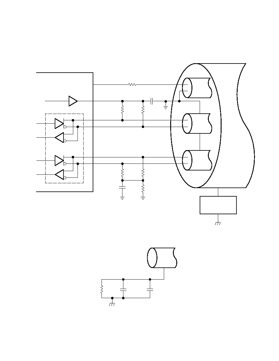
3≠29
3.10 IEEE 1394 Application Information
3.10.1 PHY Port Cable Connection
TPA+
TPA≠
TPB+
TPB≠
Cable Port
CPS
TPBIAS
56
56
56
56
5 k
1
µ
F
400 k
220 pF
(see Note A)
PCI7x20
Cable
Power
Pair
Cable
Pair
A
Cable
Pair
B
Outer Shield
Termination
NOTE A: IEEE Std 1394-1995 calls for a 250-pF capacitor, which is a nonstandard component value. A 220-pF capacitor is recommended.
Figure 3≠16. TP Cable Connections
1 M
0.001
µ
F
0.01
µ
F
Outer Cable Shield
Chassis Ground
Figure 3≠17. Typical Compliant DC Isolated Outer Shield Termination

3≠30
Outer Cable Shield
Chassis Ground
Figure 3≠18. Non-DC Isolated Outer Shield Termination
3.10.2 Crystal Selection
The PCI7x20 device is designed to use an external 24.576-MHz crystal connected between the XI and XO terminals
to provide the reference for an internal oscillator circuit. This oscillator in turn drives a PLL circuit that generates the
various clocks required for transmission and resynchronization of data at the S100 through S400 media data rates.
A variation of less than
±
100 ppm from nominal for the media data rates is required by IEEE Std 1394-1995. Adjacent
PHYs may therefore have a difference of up to 200 ppm from each other in their internal clocks, and PHY devices
must be able to compensate for this difference over the maximum packet length. Large clock variations may cause
resynchronization overflows or underflows, resulting in corrupted packet data.
The following are some typical specifications for crystals used with the PHYs from TI in order to achieve the required
frequency accuracy and stability:
∑
Crystal mode of operation: Fundamental
∑
Frequency tolerance @ 25
∞
C: Total frequency variation for the complete circuit is
±
100 ppm. A crystal with
±
30 ppm frequency tolerance is recommended for adequate margin.
∑
Frequency stability (over temperature and age): A crystal with
±
30 ppm frequency stability is recommended
for adequate margin.
NOTE: The total frequency variation must be kept below
±
100 ppm from nominal with some
allowance for error introduced by board and device variations. Trade-offs between frequency
tolerance and stability may be made as long as the total frequency variation is less than
±
100 ppm. For example, the frequency tolerance of the crystal may be specified at 50 ppm and
the temperature tolerance may be specified at 30 ppm to give a total of 80 ppm possible
variation due to the crystal alone. Crystal aging also contributes to the frequency variation.
∑
Load capacitance: For parallel resonant mode crystal circuits, the frequency of oscillation is dependent
upon the load capacitance specified for the crystal. Total load capacitance (C
L
) is a function of not only the
discrete load capacitors, but also board layout and circuit. It is recommended that load capacitors with a
maximum of
±
5% tolerance be used.
For example, load capacitors (C9 and C10 in Figure 3≠19) of 16 pF each were appropriate for the layout of the
PCI7x20 evaluation module (EVM), which uses a crystal specified for 12-pF loading. The load specified for the crystal
includes the load capacitors (C9 and C10), the loading of the PHY pins (C
PHY
), and the loading of the board itself
(C
BD
). The value of C
PHY
is typically about 1 pF, and C
BD
is typically 0.8 pF per centimeter of board etch; a typical
board can have 3 pF to 6 pF or more. The load capacitors C9 and C10 combine as capacitors in series so that the
total load capacitance is:
C
L
+
C9
C10
C9
)
C10
)
C
PHY
)
C
BD

3≠31
X1
24.576 MHz
IS
X1
CPHY + CBD
X0
C10
C9
Figure 3≠19. Load Capacitance for the PCI7x20 PHY
The layout of the crystal portion of the PHY circuit is important for obtaining the correct frequency, minimizing noise
introduced into the PHY phase-lock loop, and minimizing any emissions from the circuit. The crystal and two load
capacitors must be considered as a unit during layout. The crystal and the load capacitors must be placed as close
as possible to one another while minimizing the loop area created by the combination of the three components.
Varying the size of the capacitors may help in this. Minimizing the loop area minimizes the effect of the resonant
current (Is) that flows in this resonant circuit. This layout unit (crystal and load capacitors) must then be placed as
close as possible to the PHY X1 and X0 terminals to minimize etch lengths, as shown in Figure 3≠20.
C9
C10
X1
For more details on crystal selection, see application report SLLA051 available from the TI website:
http://www.ti.com/sc/1394.
Figure 3≠20. Recommended Crystal and Capacitor Layout
3.10.3 Bus Reset
In the PCI7x20 device, the initiate bus reset (IBR) bit may be set to 1 in order to initiate a bus reset and initialization
sequence. The IBR bit is located in PHY register 1, along with the root-holdoff bit (RHB) and Gap_Count field, as
required by IEEE Std 1394a-2000. Therefore, whenever the IBR bit is written, the RHB and Gap_Count are also
written.
The RHB and Gap_Count may also be updated by PHY-config packets. The PCI7x20 device is IEEE 1394a-2000
compliant, and therefore both the reception and transmission of PHY-config packets cause the RHB and Gap_Count
to be loaded, unlike older IEEE 1394-1995 compliant PHY devices which decode only received PHY-config packets.
The gap-count is set to the maximum value of 63 after 2 consecutive bus resets without an intervening write to the
Gap_Count, either by a write to PHY register 1 or by a PHY-config packet. This mechanism allows a PHY-config
packet to be transmitted and then a bus reset initiated so as to verify that all nodes on the bus have updated their
RHBs and Gap_Count values, without having the Gap_Count set back to 63 by the bus reset. The subsequent
connection of a new node to the bus, which initiates a bus reset, then causes the Gap_Count of each node to be set
to 63. Note, however, that if a subsequent bus reset is instead initiated by a write to register 1 to set the IBR bit, all
other nodes on the bus have their Gap_Count values set to 63, while this node Gap_Count remains set to the value
just loaded by the write to PHY register 1.

3≠32
Therefore, in order to maintain consistent gap-counts throughout the bus, the following rules apply to the use of the
IBR bit, RHB, and Gap_Count in PHY register 1:
∑
Following the transmission of a PHY-config packet, a bus reset must be initiated in order to verify that all
nodes have correctly updated their RHBs and Gap_Count values and to ensure that a subsequent new
connection to the bus causes the Gap_Count to be set to 63 on all nodes in the bus. If this bus reset is
initiated by setting the IBR bit to 1, then the RHB and Gap_Count field must also be loaded with the correct
values consistent with the just transmitted PHY-config packet. In the PCI7x20 device, the RHB and
Gap_Count are updated to their correct values upon the transmission of the PHY-config packet, so these
values may first be read from register 1 and then rewritten.
∑
Other than to initiate the bus reset, which must follow the transmission of a PHY-config packet, whenever
the IBR bit is set to 1 in order to initiate a bus reset, the Gap_Count value must also be set to 63 so as to
be consistent with other nodes on the bus, and the RHB must be maintained with its current value.
∑
The PHY register 1 must not be written to except to set the IBR bit. The RHB and Gap_Count must not be
written without also setting the IBR bit to 1.

4≠1
4 PC Card Controller Programming Model
This chapter describes the PCI7x20 PCI configuration registers that make up the 256-byte PCI configuration header
for each PCI7x20 function. There are some bits which affect both CardBus functions, but which, in order to work
properly, must be accessed only through function 0. These are called global bits. Registers containing one or more
global bits are denoted by ß in Table 4≠2.
Any bit followed by a is not cleared by the assertion of PRST (see CardBus Bridge Power Management,
Section 3.9.10, for more details) if PME is enabled (PCI offset A4h, bit 8). In this case, these bits are cleared only by
GRST. If PME is not enabled, then these bits are cleared by GRST or PRST. These bits are sometimes referred to
as PME context bits and are implemented to allow PME context to be preserved during the transition from D3
hot
or
D3
cold
to D0.
If a bit is followed by a , then this bit is cleared only by GRST in all cases (not conditional on PME being enabled).
These bits are intended to maintain device context such as interrupt routing and MFUNC programming during warm
resets.
A bit description table, typically included when the register contains bits of more than one type or purpose, indicates
bit field names, a detailed field description, and field access tags which appear in the type column. Table 4≠1
describes the field access tags.
Table 4≠1. Bit Field Access Tag Descriptions
ACCESS TAG
NAME
MEANING
R
Read
Field can be read by software.
W
Write
Field can be written by software to any value.
S
Set
Field can be set by a write of 1. Writes of 0 have no effect.
C
Clear
Field can be cleared by a write of 1. Writes of 0 have no effect.
U
Update
Field can be autonomously updated by the PCI7x20 device.
4.1
PCI Configuration Register Map (Functions 0 and 1)
The PCI7x20 is a multifunction PCI device, and the PC Card controller is integrated as PCI functions 0 and 1. The
configuration header, compliant with the PCI Local Bus Specification as a CardBus bridge header, is PC99/PC2001
compliant as well. Table 4≠2 illustrates the PCI configuration register map, which includes both the predefined portion
of the configuration space and the user-definable registers.
Table 4≠2. Functions 0 and 1 PCI Configuration Register Map
REGISTER NAME
OFFSET
Device ID
Vendor ID
00h
Status
Command
04h
Class code
Revision ID
08h
BIST
Header type
Latency timer
Cache line size
0Ch
CardBus socket registers/ExCA base address register
10h
Secondary status
Reserved
Capability pointer
14h
CardBus latency timer
Subordinate bus number
CardBus bus number
PCI bus number
18h
CardBus memory base register 0
1Ch
CardBus memory limit register 0
20h
CardBus memory base register 1
24h
CardBus memory limit register 1
28h
One or more bits in this register are cleared only by the assertion of GRST.

4≠2
Table 4≠2. Functions 0 and 1 PCI Configuration Register Map (Continued)
REGISTER NAME
OFFSET
CardBus I/O base register 0
2Ch
CardBus I/O limit register 0
30h
CardBus I/O base register 1
34h
CardBus I/O limit register 1
38h
Bridge control
Interrupt pin
Interrupt line
3Ch
Subsystem ID
Subsystem vendor ID
40h
PC Card 16-bit I/F legacy-mode base-address
44h
Reserved
48h≠7Ch
System control ß
80h
General control ß
Reserved
MC_CD debounce
84h
General-purpose output
General-purpose input
General-purpose event
enable
General-purpose event
status
88h
Multifunction routing status
8Ch
Diagnostic ß
Device control ß
Card control ß
Retry status ß
90h
Reserved
94h≠9Ch
Power management capabilities
Next item pointer
Capability ID
A0h
Power management data
(Reserved)
Power management
control/status bridge support
extensions
Power management control/status
A4h
Reserved
A8h≠ACh
Serial bus control/status
Serial bus slave address
Serial bus index
Serial bus data
B0h
Reserved
B4h≠FCh
One or more bits in this register are PME context bits and can be cleared only by the assertion of GRST when PME is enabled. If PME is not
enabled, then this bit is cleared by the assertion of PRST or GRST.
One or more bits in this register are cleared only by the assertion of GRST.
ß One or more bits in this register are global in nature and must be accessed only through function 0.
4.2
Vendor ID Register
The vendor ID register contains a value allocated by the PCI SIG that identifies the manufacturer of the PCI device.
The vendor ID assigned to Texas Instruments is 104Ch.
Bit
15
14
13
12
11
10
9
8
7
6
5
4
3
2
1
0
Name
Vendor ID
Type
R
R
R
R
R
R
R
R
R
R
R
R
R
R
R
R
Default
0
0
0
1
0
0
0
0
0
1
0
0
1
1
0
0
Register:
Vendor ID
Offset:
00h (Functions 0, 1)
Type:
Read-only
Default:
104Ch

4≠3
4.3
Device ID Register Functions 0 and 1
This read-only register contains the device ID assigned by TI to the PCI7x20 CardBus controller functions (PCI
functions 0 and 1). When Smart Card is enabled (PCI7620), the device ID is AC8Dh. When Smart Card is disabled
(PCI7420), the device ID is AC8Eh.
Bit
15
14
13
12
11
10
9
8
7
6
5
4
3
2
1
0
Name
Device ID--Smart Card enabled
Type
R
R
R
R
R
R
R
R
R
R
R
R
R
R
R
R
Default
1
0
1
0
1
1
0
0
1
0
0
0
1
1
0
1
Register:
Device ID (PCI7620)
Offset:
02h (Functions 0 and 1)
Type:
Read-only
Default:
AC8Dh
Bit
15
14
13
12
11
10
9
8
7
6
5
4
3
2
1
0
Name
Device ID--Smart Card disabled
Type
R
R
R
R
R
R
R
R
R
R
R
R
R
R
R
R
Default
1
0
1
0
1
1
0
0
1
0
0
0
1
1
1
0
Register:
Device ID (PCI7420)
Offset:
02h (Functions 0 and 1)
Type:
Read-only
Default:
AC8Eh
4≠4
4.4
Command Register
The PCI command register provides control over the PCI7x20 interface to the PCI bus. All bit functions adhere to the
definitions in the PCI Local Bus Specification (see Table 4≠3). None of the bit functions in this register are shared
among the PCI7x20 PCI functions. Three command registers exist in the PCI7x20 device, one for each function.
Software manipulates the PCI7x20 functions as separate entities when enabling functionality through the command
register. The SERR_EN and PERR_EN enable bits in this register are internally wired OR between the three
functions, and these control bits appear to software to be separate for each function.
Bit
15
14
13
12
11
10
9
8
7
6
5
4
3
2
1
0
Name
Command
Type
R
R
R
R
R
RW
R
RW
R
RW
RW
R
R
RW
RW
RW
Default
0
0
0
0
0
0
0
0
0
0
0
0
0
0
0
0
Register:
Command
Offset:
04h
Type:
Read-only, Read/Write
Default:
0000h
Table 4≠3. Command Register Description
BIT
SIGNAL
TYPE
FUNCTION
15≠11
RSVD
R
Reserved. Bits 15≠11 return 0s when read.
10
INT_DISABLE
RW
INTx disable. When set to 1, this bit disables the function from asserting interrupts on the INTx signals.
0 = INTx assertion is enabled (default)
1 = INTx assertion is disabled
9
FBB_EN
R
Fast back-to-back enable. The PCI7x20 device does not generate fast back-to-back transactions;
therefore, this bit is read-only. This bit returns a 0 when read.
8
SERR_EN
RW
System error (SERR) enable. This bit controls the enable for the SERR driver on the PCI interface. SERR
can be asserted after detecting an address parity error on the PCI bus. Both this bit and bit 6 must be set
for the PCI7x20 device to report address parity errors.
0 = Disables the SERR output driver (default)
1 = Enables the SERR output driver
7
RSVD
R
Reserved. Bit 7 returns 0 when read.
6
PERR_EN
RW
Parity error response enable. This bit controls the PCI7x20 response to parity errors through the PERR
signal. Data parity errors are indicated by asserting PERR, while address parity errors are indicated by
asserting SERR.
0 = PCI7x20 device ignores detected parity errors (default).
1 = PCI7x20 device responds to detected parity errors.
5
VGA_EN
RW
VGA palette snoop. When set to 1, palette snooping is enabled (i.e., the PCI7x20 device does not respond
to palette register writes and snoops the data). When the bit is 0, the PCI7x20 device treats all palette
accesses like all other accesses.
4
MWI_EN
R
Memory write-and-invalidate enable. This bit controls whether a PCI initiator device can generate memory
write-and-invalidate commands. The PCI7x20 controller does not support memory write-and-invalidate
commands, it uses memory write commands instead; therefore, this bit is hardwired to 0. This bit returns
0 when read. Writes to this bit have no effect.
3
SPECIAL
R
Special cycles. This bit controls whether or not a PCI device ignores PCI special cycles. The PCI7x20
device does not respond to special cycle operations; therefore, this bit is hardwired to 0. This bit returns
0 when read. Writes to this bit have no effect.
2
MAST_EN
RW
Bus master control. This bit controls whether or not the PCI7x20 device can act as a PCI bus initiator
(master). The PCI7x20 device can take control of the PCI bus only when this bit is set.
0 = Disables the PCI7x20 ability to generate PCI bus accesses (default)
1 = Enables the PCI7x20 ability to generate PCI bus accesses

4≠5
Table 4≠3. Command Register Description (continued)
BIT
SIGNAL
TYPE
FUNCTION
1
MEM_EN
RW
Memory space enable. This bit controls whether or not the PCI7x20 device can claim cycles in PCI memory
space.
0 = Disables the PCI7x20 response to memory space accesses (default)
1 = Enables the PCI7x20 response to memory space accesses
0
IO_EN
RW
I/O space control. This bit controls whether or not the PCI7x20 device can claim cycles in PCI I/O space.
0 = Disables the PCI7x20 device from responding to I/O space accesses (default)
1 = Enables the PCI7x20 device to respond to I/O space accesses
4.5
Status Register
The status register provides device information to the host system. Bits in this register can be read normally. A bit
in the status register is reset when a 1 is written to that bit location; a 0 written to a bit location has no effect. All bit
functions adhere to the definitions in the PCI Bus Specification, as seen in the bit descriptions. PCI bus status is shown
through each function. See Table 4≠4 for a complete description of the register contents.
Bit
15
14
13
12
11
10
9
8
7
6
5
4
3
2
1
0
Name
Status
Type
RW
RW
RW
RW
RW
R
R
RW
R
R
R
R
RU
R
R
R
Default
0
0
0
0
0
0
1
0
0
0
0
1
0
0
0
0
Register:
Status
Offset:
06h (Functions 0, 1)
Type:
Read-only, Read/Write
Default:
0210h
Table 4≠4. Status Register Description
BIT
SIGNAL
TYPE
FUNCTION
15
PAR_ERR
RW
Detected parity error. This bit is set when a parity error is detected, either an address or data parity error.
Write a 1 to clear this bit.
14
SYS_ERR
RW
Signaled system error. This bit is set when SERR is enabled and the PCI7x20 device signaled a system error
to the host. Write a 1 to clear this bit.
13
MABORT
RW
Received master abort. This bit is set when a cycle initiated by the PCI7x20 device on the PCI bus has been
terminated by a master abort. Write a 1 to clear this bit.
12
TABT_REC
RW
Received target abort. This bit is set when a cycle initiated by the PCI7x20 device on the PCI bus was
terminated by a target abort. Write a 1 to clear this bit.
11
TABT_SIG
RW
Signaled target abort. This bit is set by the PCI7x20 device when it terminates a transaction on the PCI bus
with a target abort. Write a 1 to clear this bit.
10≠9
PCI_SPEED
R
DEVSEL timing. These bits encode the timing of DEVSEL and are hardwired to 01b indicating that the
PCI7x20 device asserts this signal at a medium speed on nonconfiguration cycle accesses.
8
DATAPAR
RW
Data parity error detected. Write a 1 to clear this bit.
0 = The conditions for setting this bit have not been met.
1 = A data parity error occurred and the following conditions were met:
a. PERR was asserted by any PCI device including the PCI7x20.
b. The PCI7x20 device was the bus master during the data parity error.
c. The parity error response bit is set in the command register.
7
FBB_CAP
R
Fast back-to-back capable. The PCI7x20 device cannot accept fast back-to-back transactions; thus, this bit
is hardwired to 0.
6
UDF
R
UDF supported. The PCI7x20 device does not support user-definable features; therefore, this bit is
hardwired to 0.
5
66MHZ
R
66-MHz capable. The PCI7x20 device operates at a maximum PCLK frequency of 33 MHz; therefore, this
bit is hardwired to 0.
One or more bits in this register are cleared only by the assertion of GRST.

4≠6
Table 4≠4. Status Register Description (continued)
BIT
SIGNAL
TYPE
FUNCTION
4
CAPLIST
R
Capabilities list. This bit returns 1 when read. This bit indicates that capabilities in addition to standard PCI
capabilities are implemented. The linked list of PCI power-management capabilities is implemented in this
function.
3
INT_STATUS
RU
Interrupt status. This bit reflects the interrupt status of the function. Only when bit 10 (INT_DISABLE) in the
command register (PCI offset 04h, see Section 4.4) is a 0 and this bit is a 1, is the function's INTx signal
asserted. Setting the INT_DISABLE bit to a 1 has no effect on the state of this bit.
2≠0
RSVD
R
Reserved. These bits return 0s when read.
4.6
Revision ID Register
The revision ID register indicates the silicon revision of the PCI7x20 device.
Bit
7
6
5
4
3
2
1
0
Name
Revision ID
Type
R
R
R
R
R
R
R
R
Default
0
0
0
0
0
0
0
0
Register:
Revision ID
Offset:
08h (functions 0, 1)
Type:
Read-only
Default:
00h
4.7
Class Code Register
The class code register recognizes PCI7x20 functions 0 and 1 as a bridge device (06h) and a CardBus bridge device
(07h), with a 00h programming interface.
Bit
23
22
21
20
19
18
17
16
15
14
13
12
11
10
9
8
7
6
5
4
3
2
1
0
Name
PCI class code
Base class
Subclass
Programming interface
Type
R
R
R
R
R
R
R
R
R
R
R
R
R
R
R
R
R
R
R
R
R
R
R
R
Default
0
0
0
0
0
1
1
0
0
0
0
0
0
1
1
1
0
0
0
0
0
0
0
0
Register:
PCI class code
Offset:
09h (functions 0, 1)
Type:
Read-only
Default:
06 0700h
4.8
Cache Line Size Register
The cache line size register is programmed by host software to indicate the system cache line size.
Bit
7
6
5
4
3
2
1
0
Name
Cache line size
Type
RW
RW
RW
RW
RW
RW
RW
RW
Default
0
0
0
0
0
0
0
0
Register:
Cache line size
Offset:
0Ch (Functions 0, 1)
Type:
Read/Write
Default: 00h

4≠7
4.9
Latency Timer Register
The latency timer register specifies the latency timer for the PCI7x20 device, in units of PCI clock cycles. When the
PCI7x20 device is a PCI bus initiator and asserts FRAME, the latency timer begins counting from zero. If the latency
timer expires before the PCI7x20 transaction has terminated, then the PCI7x20 device terminates the transaction
when its GNT is deasserted.
Bit
7
6
5
4
3
2
1
0
Name
Latency timer
Type
RW
RW
RW
RW
RW
RW
RW
RW
Default
0
0
0
0
0
0
0
0
Register:
Latency timer
Offset:
0Dh
Type:
Read/Write
Default: 00h
4.10 Header Type Register
The header type register returns 82h when read, indicating that the PCI7x20 functions 0 and 1 configuration spaces
adhere to the CardBus bridge PCI header. The CardBus bridge PCI header ranges from PCI registers 00h≠7Fh, and
80h≠FFh is user-definable extension registers.
Bit
7
6
5
4
3
2
1
0
Name
Header type
Type
R
R
R
R
R
R
R
R
Default
1
0
0
0
0
0
1
0
Register:
Header type
Offset:
0Eh (Functions 0, 1)
Type:
Read-only
Default: 82h
4.11 BIST Register
Because the PCI7x20 device does not support a built-in self-test (BIST), this register returns the value of 00h when
read.
Bit
7
6
5
4
3
2
1
0
Name
BIST
Type
R
R
R
R
R
R
R
R
Default
0
0
0
0
0
0
0
0
Register:
BIST
Offset:
0Fh (Functions 0, 1)
Type:
Read-only
Default: 00h

4≠8
4.12 CardBus Socket Registers/ExCA Base Address Register
This register is programmed with a base address referencing the CardBus socket registers and the memory-mapped
ExCA register set. Bits 31≠12 are read/write, and allow the base address to be located anywhere in the 32-bit PCI
memory address space on a 4-Kbyte boundary. Bits 11≠0 are read-only, returning 0s when read. When software
writes all 1s to this register, the value read back is FFFF F000h, indicating that at least 4K bytes of memory address
space are required. The CardBus registers start at offset 000h, and the memory-mapped ExCA registers begin at
offset 800h. This register is not shared by functions 0 and 1, so the system maps each socket control register
separately.
Bit
31
30
29
28
27
26
25
24
23
22
21
20
19
18
17
16
Name
CardBus socket registers/ExCA base address
Type
RW
RW
RW
RW
RW
RW
RW
RW
RW
RW
RW
RW
RW
RW
RW
RW
Default
0
0
0
0
0
0
0
0
0
0
0
0
0
0
0
0
Bit
15
14
13
12
11
10
9
8
7
6
5
4
3
2
1
0
Name
CardBus socket registers/ExCA base address
Type
RW
RW
RW
RW
R
R
R
R
R
R
R
R
R
R
R
R
Default
0
0
0
0
0
0
0
0
0
0
0
0
0
0
0
0
Register:
CardBus socket registers/ExCA base address
Offset:
10h
Type:
Read-only, Read/Write
Default: 0000
0000h
4.13 Capability Pointer Register
The capability pointer register provides a pointer into the PCI configuration header where the PCI power management
register block resides. PCI header doublewords at A0h and A4h provide the power management (PM) registers. Each
socket has its own capability pointer register. This register is read-only and returns A0h when read.
Bit
7
6
5
4
3
2
1
0
Name
Capability pointer
Type
R
R
R
R
R
R
R
R
Default
1
0
1
0
0
0
0
0
Register:
Capability pointer
Offset:
14h
Type:
Read-only
Default: A0h

4≠9
4.14 Secondary Status Register
The secondary status register is compatible with the PCI-PCI bridge secondary status register. It indicates
CardBus-related device information to the host system. This register is very similar to the PCI status register (PCI
offset 06h, see Section 4.5), and status bits are cleared by a writing a 1. This register is not shared by the two socket
functions, but is accessed on a per-socket basis. See Table 4≠5 for a complete description of the register contents.
Bit
15
14
13
12
11
10
9
8
7
6
5
4
3
2
1
0
Name
Secondary status
Type
RC
RC
RC
RC
RC
R
R
RC
R
R
R
R
R
R
R
R
Default
0
0
0
0
0
0
1
0
0
0
0
0
0
0
0
0
Register:
Secondary status
Offset:
16h
Type:
Read-only, Read/Clear
Default:
0200h
Table 4≠5. Secondary Status Register Description
BIT
SIGNAL
TYPE
FUNCTION
15
CBPARITY
RC
Detected parity error. This bit is set when a CardBus parity error is detected, either an address or data
parity error. Write a 1 to clear this bit.
14
CBSERR
RC
Signaled system error. This bit is set when CSERR is signaled by a CardBus card. The PCI7x20 device
does not assert the CSERR signal. Write a 1 to clear this bit.
13
CBMABORT
RC
Received master abort. This bit is set when a cycle initiated by the PCI7x20 device on the CardBus bus
is terminated by a master abort. Write a 1 to clear this bit.
12
REC_CBTA
RC
Received target abort. This bit is set when a cycle initiated by the PCI7x20 device on the CardBus bus is
terminated by a target abort. Write a 1 to clear this bit.
11
SIG_CBTA
RC
Signaled target abort. This bit is set by the PCI7x20 device when it terminates a transaction on the CardBus
bus with a target abort. Write a 1 to clear this bit.
10≠9
CB_SPEED
R
CDEVSEL timing. These bits encode the timing of CDEVSEL and are hardwired to 01b indicating that the
PCI7x20 device asserts this signal at a medium speed.
8
CB_DPAR
RC
CardBus data parity error detected. Write a 1 to clear this bit.
0 = The conditions for setting this bit have not been met.
1 = A data parity error occurred and the following conditions were met:
a. CPERR was asserted on the CardBus interface.
b. The PCI7x20 device was the bus master during the data parity error.
c. The parity error response enable bit (bit 0) is set in the bridge control register (PCI offset 3Eh,
see Section 4.25).
7
CBFBB_CAP
R
Fast back-to-back capable. The PCI7x20 device cannot accept fast back-to-back transactions; therefore,
this bit is hardwired to 0.
6
CB_UDF
R
User-definable feature support. The PCI7x20 device does not support user-definable features; therefore,
this bit is hardwired to 0.
5
CB66MHZ
R
66-MHz capable. The PCI7x20 CardBus interface operates at a maximum CCLK frequency of 33 MHz;
therefore, this bit is hardwired to 0.
4≠0
RSVD
R
These bits return 0s when read.
One or more bits in this register are cleared only by the assertion of GRST.

4≠10
4.15 PCI Bus Number Register
The PCI bus number register is programmed by the host system to indicate the bus number of the PCI bus to which
the PCI7x20 device is connected. The PCI7x20 device uses this register in conjunction with the CardBus bus number
and subordinate bus number registers to determine when to forward PCI configuration cycles to its secondary buses.
Bit
7
6
5
4
3
2
1
0
Name
PCI bus number
Type
RW
RW
RW
RW
RW
RW
RW
RW
Default
0
0
0
0
0
0
0
0
Register:
PCI bus number
Offset:
18h (Functions 0, 1)
Type:
Read/Write
Default: 00h
4.16 CardBus Bus Number Register
The CardBus bus number register is programmed by the host system to indicate the bus number of the CardBus bus
to which the PCI7x20 device is connected. The PCI7x20 device uses this register in conjunction with the PCI bus
number and subordinate bus number registers to determine when to forward PCI configuration cycles to its secondary
buses. This register is separate for each PCI7x20 controller function.
Bit
7
6
5
4
3
2
1
0
Name
CardBus bus number
Type
RW
RW
RW
RW
RW
RW
RW
RW
Default
0
0
0
0
0
0
0
0
Register:
CardBus bus number
Offset:
19h
Type:
Read/Write
Default: 00h
4.17 Subordinate Bus Number Register
The subordinate bus number register is programmed by the host system to indicate the highest numbered bus below
the CardBus bus. The PCI7x20 device uses this register in conjunction with the PCI bus number and CardBus bus
number registers to determine when to forward PCI configuration cycles to its secondary buses. This register is
separate for each CardBus controller function.
Bit
7
6
5
4
3
2
1
0
Name
Subordinate bus number
Type
RW
RW
RW
RW
RW
RW
RW
RW
Default
0
0
0
0
0
0
0
0
Register:
Subordinate bus number
Offset:
1Ah
Type:
Read/Write
Default: 00h

4≠11
4.18 CardBus Latency Timer Register
The CardBus latency timer register is programmed by the host system to specify the latency timer for the PCI7x20
CardBus interface, in units of CCLK cycles. When the PCI7x20 device is a CardBus initiator and asserts CFRAME,
the CardBus latency timer begins counting. If the latency timer expires before the PCI7x20 transaction has
terminated, then the PCI7x20 device terminates the transaction at the end of the next data phase. A recommended
minimum value for this register of 20h allows most transactions to be completed.
Bit
7
6
5
4
3
2
1
0
Name
CardBus latency timer
Type
RW
RW
RW
RW
RW
RW
RW
RW
Default
0
0
0
0
0
0
0
0
Register:
CardBus latency timer
Offset:
1Bh (Functions 0, 1)
Type:
Read/Write
Default: 00h
4.19 CardBus Memory Base Registers 0, 1
These registers indicate the lower address of a PCI memory address range. They are used by the PCI7x20 device
to determine when to forward a memory transaction to the CardBus bus, and likewise, when to forward a CardBus
cycle to PCI. Bits 31≠12 of these registers are read/write and allow the memory base to be located anywhere in the
32-bit PCI memory space on 4-Kbyte boundaries. Bits 11≠0 are read-only and always return 0s. Writes to these bits
have no effect. Bits 8 and 9 of the bridge control register (PCI offset 3Eh, see Section 4.25) specify whether memory
windows 0 and 1 are prefetchable or nonprefetchable. The memory base register or the memory limit register must
be nonzero in order for the PCI7x20 device to claim any memory transactions through CardBus memory windows
(i.e., these windows by default are not enabled to pass the first 4 Kbytes of memory to CardBus).
Bit
31
30
29
28
27
26
25
24
23
22
21
20
19
18
17
16
Name
Memory base registers 0, 1
Type
RW
RW
RW
RW
RW
RW
RW
RW
RW
RW
RW
RW
RW
RW
RW
RW
Default
0
0
0
0
0
0
0
0
0
0
0
0
0
0
0
0
Bit
15
14
13
12
11
10
9
8
7
6
5
4
3
2
1
0
Name
Memory base registers 0, 1
Type
RW
RW
RW
RW
R
R
R
R
R
R
R
R
R
R
R
R
Default
0
0
0
0
0
0
0
0
0
0
0
0
0
0
0
0
Register:
Memory base registers 0, 1
Offset:
1Ch, 24h
Type:
Read-only, Read/Write
Default: 0000 0000h

4≠12
4.20 CardBus Memory Limit Registers 0, 1
These registers indicate the upper address of a PCI memory address range. They are used by the PCI7x20 device
to determine when to forward a memory transaction to the CardBus bus, and likewise, when to forward a CardBus
cycle to PCI. Bits 31≠12 of these registers are read/write and allow the memory base to be located anywhere in the
32-bit PCI memory space on 4-Kbyte boundaries. Bits 11≠0 are read-only and always return 0s. Writes to these bits
have no effect. Bits 8 and 9 of the bridge control register (PCI offset 3Eh, see Section 4.25) specify whether memory
windows 0 and 1 are prefetchable or nonprefetchable. The memory base register or the memory limit register must
be nonzero in order for the PCI7x20 device to claim any memory transactions through CardBus memory windows
(i.e., these windows by default are not enabled to pass the first 4 Kbytes of memory to CardBus).
Bit
31
30
29
28
27
26
25
24
23
22
21
20
19
18
17
16
Name
Memory limit registers 0, 1
Type
RW
RW
RW
RW
RW
RW
RW
RW
RW
RW
RW
RW
RW
RW
RW
RW
Default
0
0
0
0
0
0
0
0
0
0
0
0
0
0
0
0
Bit
15
14
13
12
11
10
9
8
7
6
5
4
3
2
1
0
Name
Memory limit registers 0, 1
Type
RW
RW
RW
RW
R
R
R
R
R
R
R
R
R
R
R
R
Default
0
0
0
0
0
0
0
0
0
0
0
0
0
0
0
0
Register:
Memory limit registers 0, 1
Offset:
20h, 28h
Type:
Read-only, Read/Write
Default: 0000 0000h
4.21 CardBus I/O Base Registers 0, 1
These registers indicate the lower address of a PCI I/O address range. They are used by the PCI7x20 device to
determine when to forward an I/O transaction to the CardBus bus, and likewise, when to forward a CardBus cycle
to the PCI bus. The lower 16 bits of this register locate the bottom of the I/O window within a 64-Kbyte page. The upper
16 bits (31≠16) are all 0s, which locates this 64-Kbyte page in the first page of the 32-bit PCI I/O address space. Bits
31≠2 are read/write and always return 0s forcing I/O windows to be aligned on a natural doubleword boundary in the
first 64-Kbyte page of PCI I/O address space. Bits 1≠0 are read-only, returning 00 or 01 when read, depending on
the value of bit 11 (IO_BASE_SEL) in the general control register (PCI offset 86h, see Section 4.31). These I/O
windows are enabled when either the I/O base register or the I/O limit register is nonzero. The I/O windows by default
are not enabled to pass the first doubleword of I/O to CardBus.
Either the I/O base register or the I/O limit register must be nonzero to enable any I/O transactions.
Bit
31
30
29
28
27
26
25
24
23
22
21
20
19
18
17
16
Name
I/O base registers 0, 1
Type
RW
RW
RW
RW
RW
RW
RW
RW
RW
RW
RW
RW
RW
RW
RW
RW
Default
0
0
0
0
0
0
0
0
0
0
0
0
0
0
0
0
Bit
15
14
13
12
11
10
9
8
7
6
5
4
3
2
1
0
Name
I/O base registers 0, 1
Type
RW
RW
RW
RW
RW
RW
RW
RW
RW
RW
RW
RW
RW
RW
R
R
Default
0
0
0
0
0
0
0
0
0
0
0
0
0
0
0
X
Register:
I/O base registers 0, 1
Offset:
2Ch, 34h
Type:
Read-only, Read/Write
Default: 0000 000Xh

4≠13
4.22 CardBus I/O Limit Registers 0, 1
These registers indicate the upper address of a PCI I/O address range. They are used by the PCI7x20 device to
determine when to forward an I/O transaction to the CardBus bus, and likewise, when to forward a CardBus cycle
to PCI. The lower 16 bits of this register locate the top of the I/O window within a 64-Kbyte page, and the upper 16
bits are a page register which locates this 64-Kbyte page in 32-bit PCI I/O address space. Bits 15≠2 are read/write
and allow the I/O limit address to be located anywhere in the 64-Kbyte page (indicated by bits 31≠16 of the appropriate
I/O base register) on doubleword boundaries.
Bits 31≠16 are read-only and always return 0s when read. The page is set in the I/O base register. Bits 15≠2 are
read/write and bits 1≠0 are read-only, returning 00 or 01 when read, depending on the value of bit 12 (IO_LIMIT_SEL)
in the general control register (PCI offset 86h, see Section 4.31). Writes to read-only bits have no effect.
These I/O windows are enabled when either the I/O base register or the I/O limit register is nonzero. By default, the
I/O windows are not enabled to pass the first doubleword of I/O to CardBus.
Either the I/O base register or the I/O limit register must be nonzero to enable any I/O transactions.
Bit
31
30
29
28
27
26
25
24
23
22
21
20
19
18
17
16
Name
I/O limit registers 0, 1
Type
R
R
R
R
R
R
R
R
R
R
R
R
R
R
R
R
Default
0
0
0
0
0
0
0
0
0
0
0
0
0
0
0
0
Bit
15
14
13
12
11
10
9
8
7
6
5
4
3
2
1
0
Name
I/O limit registers 0, 1
Type
RW
RW
RW
RW
RW
RW
RW
RW
RW
RW
RW
RW
RW
RW
R
R
Default
0
0
0
0
0
0
0
0
0
0
0
0
0
0
0
X
Register:
I/O limit registers 0, 1
Offset:
30h, 38h
Type:
Read-only, Read/Write
Default: 0000 000Xh
4.23 Interrupt Line Register
The interrupt line register is a read/write register used by the host software. As part of the interrupt routing procedure,
the host software writes this register with the value of the system IRQ assigned to the function.
Bit
7
6
5
4
3
2
1
0
Name
Interrupt line
Type
RW
RW
RW
RW
RW
RW
RW
RW
Default
1
1
1
1
1
1
1
1
Register:
Interrupt line
Offset:
3Ch
Type:
Read/Write
Default: FFh

4≠14
4.24 Interrupt Pin Register
The value read from this register is function dependent. The default value for function 0 is 01h (INTA), and the default
value for function 1 is 02h (INTB), the default value for function 2 is 03h (INTC), and the default value for function 3
is 04h (INTD). The value also depends on the values of bits 28, the tie-all bit (TIEALL), and 29, the interrupt tie bit
(INTRTIE), in the system control register (PCI offset 80h, see Section 4.29). The INTRTIE bit is compatible with
previous TI CardBus controllers, and when set to 1, ties INTB to INTA internally. The TIEALL bit ties INTA, INTB, INTC,
and INTD together internally. The internal interrupt connections set by INTRTIE and TIEALL are communicated to
host software through this standard register interface. This read-only register is described for all PCI7x20 functions
in Table 4≠6.
PCI function 0
Bit
7
6
5
4
3
2
1
0
Name
Interrupt pin ≠ PCI function 0
Type
R
R
R
R
R
R
R
R
Default
0
0
0
0
0
0
0
1
PCI function 1
Bit
7
6
5
4
3
2
1
0
Name
Interrupt pin ≠ PCI function 1
Type
R
R
R
R
R
R
R
R
Default
0
0
0
0
0
0
1
0
PCI function 2
Bit
7
6
5
4
3
2
1
0
Name
Interrupt pin ≠ PCI function 2
Type
R
R
R
R
R
R
R
R
Default
0
0
0
0
0
0
1
1
PCI function 3
Bit
7
6
5
4
3
2
1
0
Name
Interrupt pin ≠ PCI function 3
Type
R
R
R
R
R
R
R
R
Default
0
0
0
0
0
1
0
0
Register:
Interrupt pin
Offset:
3Dh
Type:
Read-only
Default:
01h (function 0), 02h (function 1), 03h (function 2), 04h (function 3)
Table 4≠6. Interrupt Pin Register Cross Reference
INTRTIE BIT
(BIT 29, OFFSET 80h)
TIEALL BIT
(BIT 28, OFFSET 80h)
INTPIN
FUNCTION 0
(CARDBUS)
INTPIN
FUNCTION 1
(CARDBUS)
INTPIN
FUNCTION 2
(1394 OHCI)
INTPIN
FUNCTION 3
(FLASH MEDIA)
0
0
01h (INTA)
02h (INTB)
03h (INTC)
Determined by bits 6≠5
(INT SEL field) in flash media
1
0
01h (INTA)
01h (INTA)
03h (INTC)
(INT_SEL field) in flash media
general control register (see
Section 11.21)
X
1
01h (INTA)
01h (INTA)
01h (INTA)
01h (INTA)
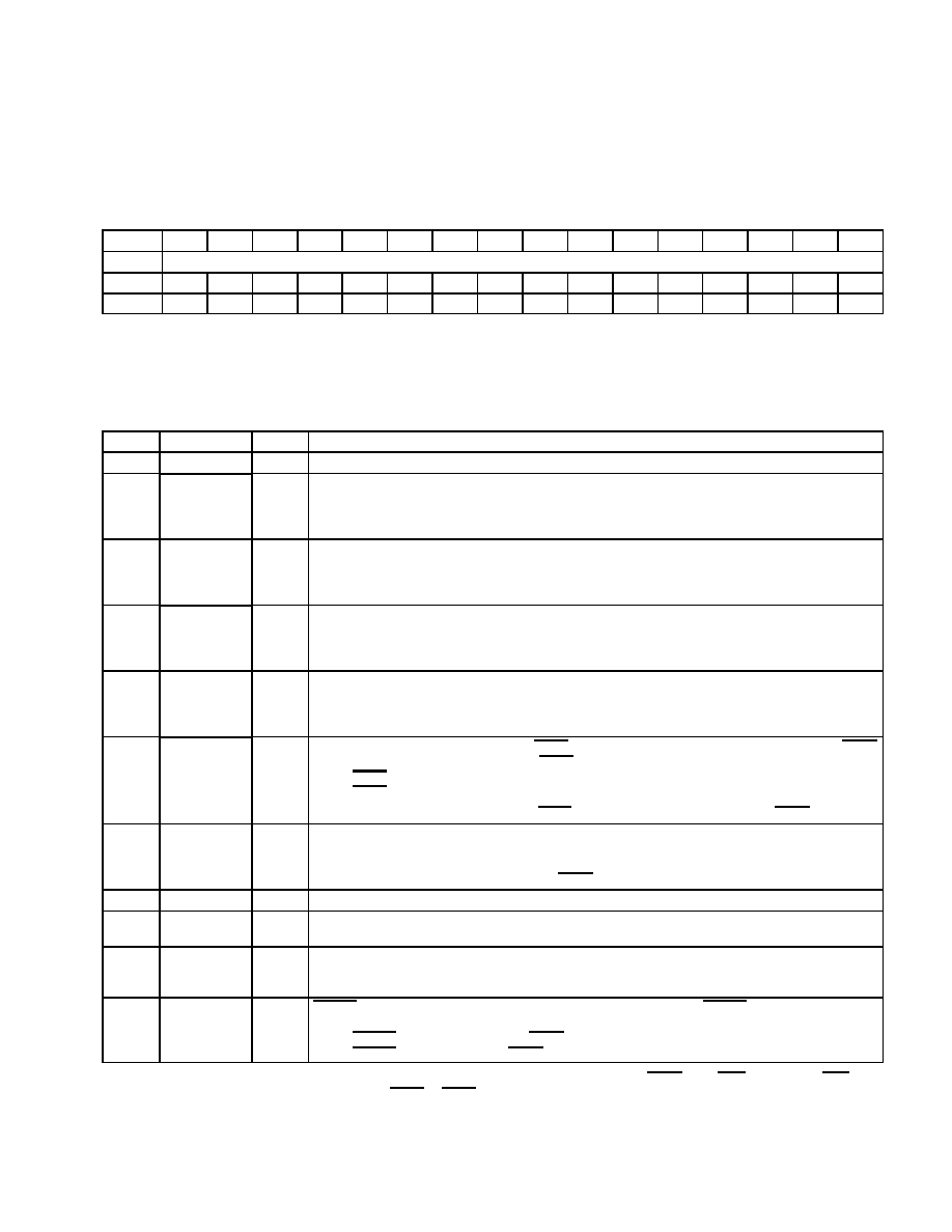
4≠15
4.25 Bridge Control Register
The bridge control register provides control over various PCI7x20 bridging functions. Some bits in this register are
global in nature and must be accessed only through function 0. See Table 4≠7 for a complete description of the
register contents.
Bit
15
14
13
12
11
10
9
8
7
6
5
4
3
2
1
0
Name
Bridge control
Type
R
R
R
R
R
RW
RW
RW
RW
RW
RW
R
RW
RW
RW
RW
Default
0
0
0
0
0
0
1
1
0
1
0
0
0
0
0
0
Register:
Bridge control
Offset:
3Eh (Function 0, 1)
Type:
Read-only, Read/Write
Default: 0340h
Table 4≠7. Bridge Control Register Description
BIT
SIGNAL
TYPE
FUNCTION
15≠11
RSVD
R
These bits return 0s when read.
10
POSTEN
RW
Write posting enable. Enables write posting to and from the CardBus sockets. Write posting enables the
posting of write data on burst cycles. Operating with write posting disabled impairs performance on burst
cycles. Note that burst write data can be posted, but various write transactions may not. This bit is socket
dependent and is not shared between functions 0 and 1.
9
PREFETCH1
RW
Memory window 1 type. This bit specifies whether or not memory window 1 is prefetchable. This bit is
socket dependent. This bit is encoded as:
0 = Memory window 1 is nonprefetchable.
1 = Memory window 1 is prefetchable (default).
8
PREFETCH0
RW
Memory window 0 type. This bit specifies whether or not memory window 0 is prefetchable. This bit is
socket dependent. This bit is encoded as:
0 = Memory window 0 is nonprefetchable.
1 = Memory window 0 is prefetchable (default).
7
INTR
RW
PCI interrupt ≠ IREQ routing enable. This bit is used to select whether PC Card functional interrupts are
routed to PCI interrupts or to the IRQ specified in the ExCA registers.
0 = Functional interrupts are routed to PCI interrupts (default).
1 = Functional interrupts are routed by ExCA registers.
6
CRST
RW
CardBus reset. When this bit is set, the CRST signal is asserted on the CardBus interface. The CRST
signal can also be asserted by passing a PRST assertion to CardBus.
0 = CRST is deasserted.
1 = CRST is asserted (default).
This bit is not cleared by the assertion of PRST. It is only cleared by the assertion of GRST.
5
MABTMODE
RW
Master abort mode. This bit controls how the PCI7x20 device responds to a master abort when the
PCI7x20 device is an initiator on the CardBus interface. This bit is common between each socket.
0 = Master aborts not reported (default).
1 = Signal target abort on PCI and signal SERR, if enabled.
4
RSVD
R
This bit returns 0 when read.
3
VGAEN
RW
VGA enable. This bit affects how the PCI7x20 device responds to VGA addresses. When this bit is set,
accesses to VGA addresses are forwarded.
2
ISAEN
RW
ISA mode enable. This bit affects how the PCI7x20 device passes I/O cycles within the 64-Kbyte ISA
range. This bit is not common between sockets. When this bit is set, the PCI7x20 device does not forward
the last 768 bytes of each 1K I/O range to CardBus.
1
CSERREN
RW
CSERR enable. This bit controls the response of the PCI7x20 device to CSERR signals on the CardBus
bus. This bit is separate for each socket.
0 = CSERR is not forwarded to PCI SERR (default)
1 = CSERR is forwarded to PCI SERR.
One or more bits in this register are PME context bits and can be cleared only by the assertion of GRST when PME is enabled. If PME is not
enabled, then this bit is cleared by the assertion of PRST or GRST.

4≠16
Table 4≠7. Bridge Control Register Description (Continued)
BIT
SIGNAL
TYPE
FUNCTION
0
CPERREN
RW
CardBus parity error response enable. This bit controls the response of the PCI7x20 to CardBus parity
errors. This bit is separate for each socket.
0 = CardBus parity errors are ignored (default).
1 = CardBus parity errors are reported using CPERR.
4.26 Subsystem Vendor ID Register
The subsystem vendor ID register, used for system and option card identification purposes, may be required for
certain operating systems. This register is read-only or read/write, depending on the setting of bit 5 (SUBSYSRW)
in the system control register (PCI offset 80h, See Section 4.29). When bit 5 is 0, this register is read/write; when bit 5
is 1, this register is read-only. The default mode is read-only. All bits in this register are reset by GRST only.
Bit
15
14
13
12
11
10
9
8
7
6
5
4
3
2
1
0
Name
Subsystem vendor ID
Type
R
R
R
R
R
R
R
R
R
R
R
R
R
R
R
R
Default
0
0
0
0
0
0
0
0
0
0
0
0
0
0
0
0
Register:
Subsystem vendor ID
Offset:
40h (Functions 0, 1)
Type:
Read-only, (Read/Write when bit 5 in the system control register is 0)
Default: 0000h
4.27 Subsystem ID Register
The subsystem ID register, used for system and option card identification purposes, may be required for certain
operating systems. This register is read-only or read/write, depending on the setting of bit 5 (SUBSYSRW) in the
system control register (PCI offset 80h, see Section 4.29). When bit 5 is 0, this register is read/write; when bit 5 is
1, this register is read-only. The default mode is read-only. All bits in this register are reset by GRST only.
If an EEPROM is present, then the subsystem ID and subsystem vendor ID is loaded from the EEPROM after a reset.
Bit
15
14
13
12
11
10
9
8
7
6
5
4
3
2
1
0
Name
Subsystem ID
Type
R
R
R
R
R
R
R
R
R
R
R
R
R
R
R
R
Default
0
0
0
0
0
0
0
0
0
0
0
0
0
0
0
0
Register:
Subsystem ID
Offset:
42h (Functions 0, 1)
Type:
Read-only, (Read/Write when bit 5 in the system control register is 0)
Default: 0000h

4≠17
4.28 PC Card 16-Bit I/F Legacy-Mode Base-Address Register
The PCI7x20 device supports the index/data scheme of accessing the ExCA registers, which is mapped by this
register. An address written to this register is the address for the index register and the address+1 is the data address.
Using this access method, applications requiring index/data ExCA access can be supported. The base address can
be mapped anywhere in 32-bit I/O space on a word boundary; hence, bit 0 is read-only, returning 1 when read. As
specified in the PCI to PCMCIA CardBus Bridge Register Description specification, this register is shared by functions
0 and 1. See the ExCA register set description in Section 5 for register offsets. All bits in this register are reset by
GRST only.
Bit
31
30
29
28
27
26
25
24
23
22
21
20
19
18
17
16
Name
PC Card 16-bit I/F legacy-mode base-address
Type
RW
RW
RW
RW
RW
RW
RW
RW
RW
RW
RW
RW
RW
RW
RW
RW
Default
0
0
0
0
0
0
0
0
0
0
0
0
0
0
0
0
Bit
15
14
13
12
11
10
9
8
7
6
5
4
3
2
1
0
Name
PC Card 16-bit I/F legacy-mode base-address
Type
RW
RW
RW
RW
RW
RW
RW
RW
RW
RW
RW
RW
RW
RW
RW
R
Default
0
0
0
0
0
0
0
0
0
0
0
0
0
0
0
1
Register:
PC Card 16-bit I/F legacy-mode base-address
Offset:
44h (Functions 0, 1)
Type:
Read-only, Read/Write
Default: 0000 0001h
4≠18
4.29 System Control Register
System-level initializations are performed through programming this doubleword register. Some of the bits are global
in nature and must be accessed only through function 0. See Table 4≠8 for a complete description of the register
contents.
Bit
31
30
29
28
27
26
25
24
23
22
21
20
19
18
17
16
Name
System control
Type
RW
RW
RW
RW
RW
RW
RW
RW
R
RW
RW
RW
R
R
R
R
Default
0
0
0
0
1
0
0
0
0
1
0
0
0
0
0
0
Bit
15
14
13
12
11
10
9
8
7
6
5
4
3
2
1
0
Name
System control
Type
RW
RW
R
R
R
R
R
R
R
RW
RW
RW
RW
R
RW
RW
Default
1
0
0
1
0
0
0
0
0
1
1
0
0
0
0
0
Register:
System control
Offset:
80h (Functions 0, 1)
Type:
Read-only, Read/Write
Default: 0840 9060h
Table 4≠8. System Control Register Description
BIT
SIGNAL
TYPE
FUNCTION
31≠30 ß
SER_STEP
RW
Serial input stepping. In serial PCI interrupt mode, these bits are used to configure the serial stream PCI
interrupt frames, and can be used to accomplish an even distribution of interrupts signaled on the four PCI
interrupt slots.
00 = INTA/INTB/INTC/INTD signal in INTA/INTB/INTC/INTD slots (default)
01 = INTA/INTB/INTC/INTD signal in INTB/INTC/INTD/INTA slots
10 = INTA/INTB/INTC/INTD signal in INTC/INTD/INTA/INTB slots
11 = INTA/INTB/INTC/INTD signal in INTD/INTA/INTB/INTC slots
29 ß
INTRTIE
RW
This bit ties INTA to INTB internally (to INTA), and reports this through the interrupt pin register (PCI offset
3Dh, see Section 4.24). This bit has no effect on INTC or INTD.
28
TIEALL
RW
This bit ties INTA, INTB, INTC, and INTD internally (to INTA), and reports this through the interrupt pin
register (PCI offset 3Dh, see Section 4.24).
27
PSCCLK
RW
P2C power switch clock. The PCI7x20 CLOCK signal clocks the serial interface power switch and the
internal state machine. The default state for this bit is 1, allowing the internal oscillator to provide the clock
signal. Bit 27 can be set to 0, requiring an external clock source provided to the CLOCK terminal.
0 = CLOCK is provided externally, input to the PCI7x20 device.
1 = CLOCK is generated by the internal oscillator and driven by the PCI7x20 device. (default)
26 ß
SMIROUTE
RW
SMI interrupt routing. This bit is shared between functions 0 and 1, and selects whether IRQ2 or CSC is
signaled when a write occurs to power a PC Card socket.
0 = PC Card power change interrupts are routed to IRQ2 (default).
1 = A CSC interrupt is generated on PC Card power changes.
25
SMISTATUS
RW
SMI interrupt status. This socket-dependent bit is set when a write occurs to set the socket power, and
the SMIENB bit is set. Writing a 1 to this bit clears the status.
0 = SMI interrupt is signaled.
1 = SMI interrupt is not signaled.
24 ß
SMIENB
RW
SMI interrupt mode enable. When this bit is set, the SMI interrupt signaling generates an interrupt when
a write to the socket power control occurs. This bit is shared and defaults to 0 (disabled).
0 = SMI interrupt mode is disabled (default).
1 = SMI interrupt mode is enabled.
23
RSVD
R
Reserved
One or more bits in this register are cleared only by the assertion of GRST.
ß These bits are global in nature and must be accessed only through function 0.

4≠19
Table 4≠8
.
System Control Register Description (continued)
BIT
SIGNAL
TYPE
FUNCTION
22
CBRSVD
RW
CardBus reserved terminals signaling. When this bit is set, the RSVD CardBus terminals are driven
low when a CardBus card has been inserted. When this bit is low, these signals are placed in a
high-impedance state.
0 = Place the CardBus RSVD terminals in a high-impedance state.
1 = Drive the CardBus RSVD terminals low (default).
21
VCCPROT
RW
VCC protection enable. This bit is socket dependent.
0 = VCC protection is enabled for 16-bit cards (default).
1 = VCC protection is disabled for 16-bit cards.
20≠16
RSVD
RW
These bits are reserved. Do not change the value of these bits.
15 ß
MRBURSTDN
RW
Memory read burst enable downstream. When this bit is set, the PCI7x20 device allows memory read
transactions to burst downstream.
0 = MRBURSTDN downstream is disabled.
1 = MRBURSTDN downstream is enabled (default).
14 ß
MRBURSTUP
RW
Memory read burst enable upstream. When this bit is set, the PCI7x20 device allows memory read
transactions to burst upstream.
0 = MRBURSTUP upstream is disabled (default).
1 = MRBURSTUP upstream is enabled.
13
SOCACTIVE
R
Socket activity status. When set, this bit indicates access has been performed to or from a PC Card.
Reading this bit causes it to be cleared. This bit is socket dependent.
0 = No socket activity (default)
1 = Socket activity
12
RSVD
R
Reserved. This bit returns 1 when read.
11
PWRSTREAM
R
Power-stream-in-progress status bit. When set, this bit indicates that a power stream to the power
switch is in progress and a powering change has been requested. When this bit is cleared, it indicates
that the power stream is complete.
0 = Power stream is complete, delay has expired (default).
1 = Power stream is in progress.
10
DELAYUP
R
Power-up delay-in-progress status bit. When set, this bit indicates that a power-up stream has been
sent to the power switch, and proper power may not yet be stable. This bit is cleared when the power-up
delay has expired.
0 = Power-up delay has expired (default).
1 = Power-up stream sent to switch. Power might not be stable.
9
DELAYDOWN
R
Power-down delay-in-progress status bit. When set, this bit indicates that a power-down stream has
been sent to the power switch, and proper power may not yet be stable. This bit is cleared when the
power-down delay has expired.
0 = Power-down delay has expired (default).
1 = Power-down stream sent to switch. Power might not be stable.
8
INTERROGATE
R
Interrogation in progress. When set, this bit indicates an interrogation is in progress, and clears when
the interrogation completes. This bit is socket-dependent.
0 = Interrogation not in progress (default)
1 = Interrogation in progress
7
RSVD
R
Reserved. This bit returns 0 when read.
6 ß
PWRSAVINGS
RW
Power savings mode enable. When this bit is set, the PCI7x20 device consumes less power with no
performance loss. This bit is shared between the two PCI7x20 CardBus functions.
0 = Power savings mode disabled
1 = Power savings mode enabled (default)
5 ß
SUBSYSRW
RW
Subsystem ID and subsystem vendor ID, ExCA ID and revision register read/write enable. This bit also
controls read/write for the function 3 subsystem ID register.
0 = Registers are read/write.
1 = Registers are read-only (default).
One or more bits in this register are PME context bits and can be cleared only by the assertion of GRST when PME is enabled. If PME is not
enabled, then this bit is cleared by the assertion of PRST or GRST.
One or more bits in this register are cleared only by the assertion of GRST.
ß These bits are global in nature and must be accessed only through function 0.
4≠20
Table 4≠8
.
System Control Register Description (continued)
BIT
SIGNAL
TYPE
FUNCTION
4 ß
CB_DPAR
RW
CardBus data parity SERR signaling enable.
0 = CardBus data parity not signaled on PCI SERR signal (default)
1 = CardBus data parity signaled on PCI SERR signal
3 ß
RSVD
R
Reserved. This bit returns 0 when read.
2
EXCAPOWER
R
ExCA power control bit.
0 = Enables 3.3 V (default)
1 = Enables 5 V
1 ß
KEEPCLK
RW
Keep clock. When this bit is set, the PCI7x20 device follows the CLKRUN protocol to maintain the
system PCLK and the CCLK (CardBus clock). This bit is global to the PCI7x20 functions.
0 = Allow system PCLK and CCLK clocks to stop (default)
1 = Never allow system PCLK or CCLK clock to stop
Note that the functionality of this bit has changed relative to that of the PCI12XX family of TI CardBus
controllers. In these CardBus controllers, setting this bit only maintains the PCI clock, not the CCLK.
In the PCI7x20 device, setting this bit maintains both the PCI clock and the CCLK.
0 ß
RIMUX
RW
PME/RI_OUT select bit. When this bit is 1, the PME signal is routed to the PME/RI_OUT terminal (R03).
When this bit is 0 and bit 7 (RIENB) of the card control register is 1, the RI_OUT signal is routed to the
PME/RI_OUT terminal. If this bit is 0 and bit 7 (RIENB) of the card control register is 0, then the output
is placed in a high-impedance state. This terminal is encoded as:
0 = RI_OUT signal is routed to the PME/RI_OUT terminal if bit 7 of the card control register is 1.
(default)
1 = PME signal is routed to the PME/RI_OUT terminal of the PCI7x20 controller.
NOTE: If this bit (bit 0) is 0 and bit 7 of the card control register (PCI offset 91h, see Section 4.38) is
0, then the output on the PME/RI_OUT terminal is placed in a high-impedance state.
One or more bits in this register are cleared only by the assertion of GRST.
ß These bits are global in nature and must be accessed only through function 0.
4.30 MC_CD Debounce Register
This register provides debounce time in units of 2 ms for the MC_CD signal on UltraMedia cards. This register defaults
to 19h, which gives a default debounce time of 50 ms. All bits in this register are reset by GRST only.
Bit
7
6
5
4
3
2
1
0
Name
MC_CD debounce
Type
RW
RW
RW
RW
RW
RW
RW
RW
Default
0
0
0
1
1
0
0
1
Register:
MC_CD debounce
Offset:
84h (Functions 0, 1)
Type:
Read/Write
Default: 19h

4≠21
4.31 General Control Register
The general control register provides top level PCI arbitration control. It also provides the ability to disable the 1394
OHCI function and provides control over miscellaneous new functionality. See Table 4≠9 for a complete description
of the register contents.
Bit
15
14
13
12
11
10
9
8
7
6
5
4
3
2
1
0
Name
General control
Type
R
R
RW
RW
RW
RW
R
R
R
R
RW
RW
RW
R
RW
RW
Default
0
0
0
0
0
0
0
0
1
0
0
0
0
0
0
0
Register:
General control
Offset:
86h
Type:
Read/Write, Read-only
Default: 0080h
Table 4≠9. General Control Register Description
BIT
SIGNAL
TYPE
FUNCTION
15≠14
RSVD
R
These bits do not affect any functionality within the CardBus core.
13
SIM_MODE
RW
When this bit is set, it reduces the query time for UltraMedia card types.
0 = Query time is unaffected (default)
1 = Query time is reduced for simulation purposes
12
IO_LIMIT_SEL
RW
When this bit is set, bit 0 in the I/O limit registers (PCI offsets 30h and 38h) for both CardBus functions
is set.
0 = Bit 0 in the I/O limit registers is 0 (default)
1 = Bit 0 in the I/O limit registers is 1
11
IO_BASE_SEL
RW
When this bit is set, bit 0 in the I/O base registers (PCI offsets 2Ch and 34h) for both CardBus functions
is set.
0 = Bit 0 in the I/O base registers is 0 (default)
1 = Bit 0 in the I/O base registers is 1
10
12V_SW_SEL
RW
Power switch select. This bit selects which power switch is implemented in the system.
0 = A 1.8-V capable power switch (TPS2228) is used (default)
1 = A 12-V capable power switch (TPS2226) is used
9≠8
RSVD
R
Reserved. These bits return 0 when read.
7
PCI2_3_EN
R
PCI 2.3 enable. The PCI7x20 CardBus functions always conform to the PCI 2.3 specification.
Therefore, this bit is tied to 1.
6
RSVD
R
Reserved. This bit returns 0 when read.
5
DISABLE_FM
RW
When this bit is set, the flash media function is completely nonaccessible and nonfunctional.
4
DISABLE_SKTB
RW
When this bit is set, CardBus socket B (function 1) is completely nonaccessible and nonfunctional.
3
DISABLE_OHCI
RW
When set, the OHCI 1394 controller function is completely nonaccessible and nonfunctional.
2
RSVD
R
Reserved. This bit returns 0 when read.
1≠0
ARB_CTRL
RW
Controls top level PCI arbitration:
00 = 1394 OHCI priority
10 = Flash media priority
01 = CardBus priority
11 = Fair round robin
One or more bits in this register are cleared only by the assertion of GRST.

4≠22
4.32 General-Purpose Event Status Register
The general-purpose event status register contains status bits that are set when general events occur, and can be
programmed to generate general-purpose event signaling through GPE. See Table 4≠10 for a complete description
of the register contents.
Bit
7
6
5
4
3
2
1
0
Name
General-purpose event status
Type
RCU
RCU
R
RCU
RCU
RCU
RCU
RCU
Default
0
0
0
0
0
0
0
0
Register:
General-purpose event status
Offset:
88h
Type:
Read/Clear/Update, Read-only
Default: 00h
Table 4≠10. General-Purpose Event Status Register Description
BIT
SIGNAL
TYPE
FUNCTION
7
PWR_STS
RCU
Power change status. This bit is set when software changes the VCC or VPP power state of either socket.
6
VPP12_STS
RCU
12-V VPP request status. This bit is set when software has changed the requested VPP level to or from 12 V
for either socket.
5
RSVD
R
Reserved. This bit returns 0 when read. A write has no effect.
4
GP4_STS
RCU
GPI4 status. This bit is set on a change in status of the MFUNC5 terminal input level if configured as a
general-purpose input, GPI4.
3
GP3_STS
RCU
GPI3 status. This bit is set on a change in status of the MFUNC4 terminal input level if configured as a
general-purpose input, GPI3.
2
GP2_STS
RCU
GPI2 status. This bit is set on a change in status of the MFUNC2 terminal input level if configured as a
general-purpose input, GPI2.
1
GP1_STS
RCU
GPI1 status. This bit is set on a change in status of the MFUNC1 terminal input level if configured as a
general-purpose input, GPI1.
0
GP0_STS
RCU
GPI0 status. This bit is set on a change in status of the MFUNC0 terminal input level if configured as a
general-purpose input, GPI0.
One or more bits in this register are cleared only by the assertion of GRST.

4≠23
4.33 General-Purpose Event Enable Register
The general-purpose event enable register contains bits that are set to enable GPE signals. See Table 4≠11 for a
complete description of the register contents.
Bit
7
6
5
4
3
2
1
0
Name
General-purpose event enable
Type
RW
RW
R
RW
RW
RW
RW
RW
Default
0
0
0
0
0
0
0
0
Register:
General-purpose event enable
Offset:
89h
Type:
Read-only, Read/Write
Default: 00h
Table 4≠11. General-Purpose Event Enable Register Description
BIT
SIGNAL
TYPE
FUNCTION
7
PWR_EN
RW
Power change GPE enable. When this bit is set, GPE is signaled on PWR_STS events.
6
VPP12_EN
RW
12-V VPP GPE enable. When this bit is set, GPE is signaled on VPP12_STS events.
5
RSVD
R
Reserved. This bit returns 0 when read. A write has no effect.
4
GP4_EN
RW
GPI4 GPE enable. When this bit is set, GPE is signaled on GP4_STS events.
3
GP3_EN
RW
GPI3 GPE enable. When this bit is set, GPE is signaled on GP3_STS events.
2
GP2_EN
RW
GPI2 GPE enable. When this bit is set, GPE is signaled on GP2_STS events.
1
GP1_EN
RW
GPI1 GPE enable. When this bit is set, GPE is signaled on GP1_STS events.
0
GP0_EN
RW
GPI0 GPE enable. When this bit is set, GPE is signaled on GP0_STS events.
One or more bits in this register are cleared only by the assertion of GRST.
4.34 General-Purpose Input Register
The general-purpose input register contains the logical value of the data input to the GPI terminals. See Table 4≠12
for a complete description of the register contents.
Bit
7
6
5
4
3
2
1
0
Name
General-purpose input
Type
R
R
R
RU
RU
RU
RU
RU
Default
0
0
0
X
X
X
X
X
Register:
General-purpose input
Offset:
8Ah
Type:
Read/Update, Read-only
Default: XXh
Table 4≠12. General-Purpose Input Register Description
BIT
SIGNAL
TYPE
FUNCTION
7≠5
RSVD
R
Reserved. These bits return 0s when read. Writes have no effect.
4
GPI4_DATA
RU
GPI4 data input. This bit represents the logical value of the data input from GPI4.
3
GPI3_DATA
RU
GPI3 data input. This bit represents the logical value of the data input from GPI3.
2
GPI2_DATA
RU
GPI2 data input. This bit represents the logical value of the data input from GPI2.
1
GPI1_DATA
RU
GPI1 data input. This bit represents the logical value of the data input from GPI1.
0
GPI0_DATA
RU
GPI0 data input. This bit represents the logical value of the data input from GPI0.

4≠24
4.35 General-Purpose Output Register
The general-purpose output register is used to drive the GPO4≠GPO0 outputs. See Table 4≠13 for a complete
description of the register contents.
Bit
7
6
5
4
3
2
1
0
Name
General-purpose output
Type
R
R
R
RW
RW
RW
RW
RW
Default
0
0
0
0
0
0
0
0
Register:
General-purpose output
Offset:
8Bh
Type:
Read-only, Read/Write
Default: 00h
Table 4≠13. General-Purpose Output Register Description
BIT
SIGNAL
TYPE
FUNCTION
7≠5
RSVD
R
Reserved. These bits return 0s when read. Writes have no effect.
4
GPO4_DATA
RW
This bit represents the logical value of the data driven to GPO4.
3
GPO3_DATA
RW
This bit represents the logical value of the data driven to GPO3.
2
GPO2_DATA
RW
This bit represents the logical value of the data driven to GPO2.
1
GPO1_DATA
RW
This bit represents the logical value of the data driven to GPO1.
0
GPO0_DATA
RW
This bit represents the logical value of the data driven to GPO0.
One or more bits in this register are cleared only by the assertion of GRST.
4≠25
4.36 Multifunction Routing Status Register
The multifunction routing status register is used to configure the MFUNC6≠MFUNC0 terminals. These terminals may
be configured for various functions. This register is intended to be programmed once at power-on initialization. The
default value for this register can also be loaded through a serial EEPROM. See Table 4≠14 for a complete description
of the register contents.
Bit
31
30
29
28
27
26
25
24
23
22
21
20
19
18
17
16
Name
Multifunction routing status
Type
R
RW
RW
RW
R
RW
RW
RW
R
RW
RW
RW
R
RW
RW
RW
Default
0
0
0
0
0
0
0
0
0
0
0
0
0
0
0
0
Bit
15
14
13
12
11
10
9
8
7
6
5
4
3
2
1
0
Name
Multifunction routing status
Type
R
RW
RW
RW
R
RW
RW
RW
R
RW
RW
RW
R
RW
RW
RW
Default
0
0
0
1
0
0
0
0
0
0
0
0
0
0
0
0
Register:
Multifunction routing status
Offset:
8Ch
Type:
Read/Write, Read-only
Default: 0000 1000h
Table 4≠14. Multifunction Routing Status Register Description
BIT
SIGNAL
TYPE
FUNCTION
31≠28
RSVD
R
Bits 31≠28 return 0s when read.
27≠24
MFUNC6
RW
Multifunction terminal 6 configuration. These bits control the internal signal mapped to the MFUNC6 terminal
as follows:
0000 = RSVD
0100 = IRQ4
1000 = IRQ8
1100 = IRQ12
0001 = CLKRUN
0101 = IRQ5
1001 = IRQ9
1101 = IRQ13
0010 = IRQ2
0110 = IRQ6
1010 = IRQ10
1110 = IRQ14
0011 = IRQ3
0111 = IRQ7
1011 = IRQ11
1111 = IRQ15
23≠20
MFUNC5
RW
Multifunction terminal 5 configuration. These bits control the internal signal mapped to the MFUNC5 terminal
as follows:
0000 = GPI4
0100 = IRQ4
1000 = CAUDPWM
1100 = LEDA1
0001 = GPO4
0101 = IRQ5
1001 = IRQ9
1101 = LED_SKT
0010 = PCGNT
0110 = RSVD
1010 = IRQ10
1110 = GPE
0011 = IRQ3
0111 = RSVD
1011 = OHCI_LED
1111 = IRQ15
19≠16
MFUNC4
RW
Multifunction terminal 4 configuration. These bits control the internal signal mapped to the MFUNC4 terminal
as follows:
0000 = GPI3
0100 = IRQ4
1000 = CAUDPWM
1100 = RI_OUT
0001 = GPO3
0101 = IRQ5
1001 = IRQ9
1101 = LED_SKT
0010 = LOCK PCI
0110 = RSVD
1010 = INTD
1110 = GPE
0011 = IRQ3
0111 = RSVD
1011 = IRQ11
1111 = IRQ15
15≠12
MFUNC3
RW
Multifunction terminal 3 configuration. These bits control the internal signal mapped to the MFUNC3 terminal
as follows:
0000 = RSVD
0100 = IRQ4
1000 = IRQ8
1100 = IRQ12
0001 = IRQSER
0101 = IRQ5
1001 = IRQ9
1101 = IRQ13
0010 = IRQ2
0110 = IRQ6
1010 = IRQ10
1110 = IRQ14
0011 = IRQ3
0111 = IRQ7
1011 = IRQ11
1111 = IRQ15
11≠8
MFUNC2
RW
Multifunction terminal 2 configuration. These bits control the internal signal mapped to the MFUNC2 terminal
as follows:
0000 = GPI2
0100 = IRQ4
1000 = CAUDPWM
1100 = RI_OUT
0001 = GPO2
0101 = IRQ5
1001 = IRQ9
1101 = TEST_MUX
0010 = PCREQ
0110 = RSVD
1010 = IRQ10
1110 = GPE
0011 = IRQ3
0111 = RSVD
1011 = INTC
1111 = IRQ7
One or more bits in this register are cleared only by the assertion of GRST.

4≠26
Table 4≠14. Multifunction Routing Status Register Description (Continued)
BIT
SIGNAL
TYPE
FUNCTION
7≠4
MFUNC1
RW
Multifunction terminal 1 configuration. These bits control the internal signal mapped to the MFUNC1 terminal
as follows:
0000 = GPI1
0100 = OHCI_LED 1000 = CAUDPWM
1100 = LEDA1
0001 = GPO1
0101 = IRQ5
1001 = IRQ9
1101 = LEDA2
0010 = INTB
0110 = RSVD
1010 = IRQ10
1110 = GPE
0011 = IRQ3
0111 = RSVD
1011 = IRQ11
1111 = IRQ15
3≠0
MFUNC0
RW
Multifunction terminal 0 configuration. These bits control the internal signal mapped to the MFUNC0 terminal
as follows:
0000 = GPI0
0100 = IRQ4
1000 = CAUDPWM
1100 = LEDA1
0001 = GPO0
0101 = IRQ5
1001 = IRQ9
1101 = LEDA2
0010 = INTA
0110 = RSVD
1010 = IRQ10
1110 = GPE
0011 = IRQ3
0111 = RSVD
1011 = IRQ11
1111 = IRQ15
One or more bits in this register are cleared only by the assertion of GRST.
4.37 Retry Status Register
The contents of the retry status register enable the retry time-out counters and display the retry expiration status. The
flags are set when the PCI7x20 device, as a master, receives a retry and does not retry the request within 2
15
clock
cycles. The flags are cleared by writing a 1 to the bit. Access this register only through function 0. See Table 4≠15
for a complete description of the register contents.
Bit
7
6
5
4
3
2
1
0
Name
Retry status
Type
RW
RW
RC
R
RC
R
RC
R
Default
1
1
0
0
0
0
0
0
Register:
Retry status
Offset:
90h (Functions 0, 1)
Type:
Read-only, Read/Write, Read/Clear
Default: C0h
Table 4≠15. Retry Status Register Description
BIT
SIGNAL
TYPE
FUNCTION
7
PCIRETRY
RW
PCI retry time-out counter enable. This bit is encoded as:
0 = PCI retry counter disabled
1 = PCI retry counter enabled (default)
6 ß
CBRETRY
RW
CardBus retry time-out counter enable. This bit is encoded as:
0 = CardBus retry counter disabled
1 = CardBus retry counter enabled (default)
5
TEXP_CBB
RC
CardBus target B retry expired. Write a 1 to clear this bit.
0 = Inactive (default)
1 = Retry has expired.
4
RSVD
R
Reserved. This bit returns 0 when read.
3 ß
TEXP_CBA
RC
CardBus target A retry expired. Write a 1 to clear this bit.
0 = Inactive (default)
1 = Retry has expired.
2
RSVD
R
Reserved. This bit returns 0 when read.
1
TEXP_PCI
RC
PCI target retry expired. Write a 1 to clear this bit.
0 = Inactive (default)
1 = Retry has expired.
0
RSVD
R
Reserved. This bit returns 0 when read.
One or more bits in this register are cleared only by the assertion of GRST.
ß These bits are global in nature and must be accessed only through function 0.

4≠27
4.38 Card Control Register
The card control register is provided for PCI1130 compatibility. RI_OUT is enabled through this register, and the
enable bit is shared between functions 0 and 1. See Table 4≠16 for a complete description of the register contents.
The RI_OUT signal is enabled through this register, and the enable bit is shared between functions 0 and 1.
Bit
7
6
5
4
3
2
1
0
Name
Card control
Type
RW
RW
RW
R
R
RW
RW
RW
Default
0
0
0
0
0
0
0
0
Register:
Card control
Offset:
91h
Type:
Read-only, Read/Write
Default: 00h
Table 4≠16. Card Control Register Description
BIT
SIGNAL
TYPE
FUNCTION
7 ß
RIENB
RW
Ring indicate enable. When this bit is 1, the RI_OUT output is enabled. This bit defaults to 0.
6≠3
RSVD
RW
These bits are reserved. Do not change the value of these bits.
2
AUD2MUX
RW
CardBus audio-to-MFUNC. When this bit is set, the CAUDIO CardBus signal must be routed through an
MFUNC terminal. If this bit is set for both functions, then function 0 is routed.
0 = CAUDIO set to CAUDPWM on MFUNC terminal (default)
1 = CAUDIO is not routed.
1
SPKROUTEN
RW
When bit 1 is set, the SPKR terminal from the PC Card is enabled and is routed to the SPKROUT terminal.
The SPKR signal from socket 0 is XORed with the SPKR signal from socket 1 and sent to SPKROUT. The
SPKROUT terminal drives data only when the SPKROUTEN bit of either function is set. This bit is encoded
as:
0 = SPKR to SPKROUT not enabled (default)
1 = SPKR to SPKROUT enabled
0
IFG
RW
Interrupt flag. This bit is the interrupt flag for 16-bit I/O PC Cards and for CardBus cards. This bit is set when
a functional interrupt is signaled from a PC Card interface, and is socket dependent (i.e., not global). Write
back a 1 to clear this bit.
0 = No PC Card functional interrupt detected (default)
1 = PC Card functional interrupt detected
One or more bits in this register are cleared only by the assertion of GRST.
ß This bit is global in nature and must be accessed only through function 0.
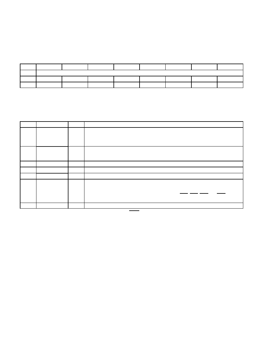
4≠28
4.39 Device Control Register
The device control register is provided for PCI1130 compatibility. It contains bits that are shared between functions
0 and 1. The interrupt mode select is programmed through this register. The socket-capable force bits are also
programmed through this register. See Table 4≠17 for a complete description of the register contents.
Bit
7
6
5
4
3
2
1
0
Name
Device control
Type
RW
RW
RW
R
RW
RW
RW
RW
Default
0
1
1
0
0
1
1
0
Register:
Device control
Offset:
92h (Functions 0, 1)
Type:
Read-only, Read/Write
Default: 66h
Table 4≠17. Device Control Register Description
BIT
SIGNAL
TYPE
FUNCTION
7
SKTPWR_LOCK
RW
Socket power lock bit. When this bit is set to 1, software cannot power down the PC Card socket while
in D3. It may be necessary to lock socket power in order to support wake on LAN or RING if the
operating system is programmed to power down a socket when the CardBus controller is placed in the
D3 state.
6 ß
3VCAPABLE
RW
3-V socket capable force bit.
0 = Not 3-V capable
1 = 3-V capable (default)
5
IO16R2
RW
Diagnostic bit. This bit defaults to 1.
4
RSVD
R
Reserved. This bit returns 0 when read. A write has no effect.
3 ß
TEST
RW
TI test bit. Write only 0 to this bit.
2≠1 ß
INTMODE
RW
Interrupt mode. These bits select the interrupt signaling mode. The interrupt mode bits are encoded:
00 = Parallel PCI interrupts only
01 = Reserved
10 = IRQ serialized interrupts and parallel PCI interrupts INTA, INTB, INTC, and INTD
11 = IRQ and PCI serialized interrupts (default)
0 ß
RSVD
RW
Reserved. Bit 0 is reserved for test purposes. Only a 0 must be written to this bit.
One or more bits in this register are cleared only by the assertion of GRST.
ß These bits are global in nature and must be accessed only through function 0.

4≠29
4.40 Diagnostic Register
The diagnostic register is provided for internal TI test purposes. It is a read/write register, but only 0s must be written
to it. See Table 4≠18 for a complete description of the register contents.
Bit
7
6
5
4
3
2
1
0
Name
Diagnostic
Type
RW
R
RW
RW
RW
RW
RW
RW
Default
0
1
1
0
0
0
0
0
Register:
Diagnostic
Offset:
93h (functions 0, 1)
Type:
Read/Write
Default:
60h
Table 4≠18. Diagnostic Register Description
BIT
SIGNAL
TYPE
FUNCTION
7 ß
TRUE_VAL
RW
This bit defaults to 0. This bit is encoded as:
0 = Reads true values in PCI vendor ID and PCI device ID registers (default)
1 = Returns all 1s to reads from the PCI vendor ID and PCI device ID registers
6
RSVD
R
Reserved. This bit is read-only and returns 1 when read.
5
CSC
RW
CSC interrupt routing control
0 = CSC interrupts routed to PCI if ExCA 803 bit 4 = 1
1 = CSC interrupts routed to PCI if ExCA 805 bits 7≠4 = 0000b (default).
In this case, the setting of ExCA 803 bit 4 is a don't care.
4 ß
DIAG4
RW
Diagnostic RETRY_DIS. Delayed transaction disable.
3 ß
DIAG3
RW
Diagnostic RETRY_EXT. Extends the latency from 16 to 64.
2 ß
DIAG2
RW
Diagnostic DISCARD_TIM_SEL_CB. Set = 210, reset = 215.
1 ß
DIAG1
RW
Diagnostic DISCARD_TIM_SEL_PCI. Set = 210, reset = 215.
0
RSVD
RW
This bit is reserved. Do not change the value of this bit.
One or more bits in this register are cleared only by the assertion of GRST.
ß This bit is global and is accessed only through function 0.

4≠30
4.41 Capability ID Register
The capability ID register identifies the linked list item as the register for PCI power management. The register returns
01h when read, which is the unique ID assigned by the PCI SIG for the PCI location of the capabilities pointer and
the value.
Bit
7
6
5
4
3
2
1
0
Name
Capability ID
Type
R
R
R
R
R
R
R
R
Default
0
0
0
0
0
0
0
1
Register:
Capability ID
Offset:
A0h
Type:
Read-only
Default: 01h
4.42 Next Item Pointer Register
The contents of this register indicate the next item in the linked list of the PCI power management capabilities.
Because the PCI7x20 functions only include one capabilities item, this register returns 0s when read.
Bit
7
6
5
4
3
2
1
0
Name
Next item pointer
Type
R
R
R
R
R
R
R
R
Default
0
0
0
0
0
0
0
0
Register:
Next item pointer
Offset:
A1h
Type:
Read-only
Default: 00h
4≠31
4.43 Power Management Capabilities Register
The power management capabilities register contains information on the capabilities of the PC Card function related
to power management. Both PCI7x20 CardBus bridge functions support D0, D1, D2, and D3 power states. Default
register value is FE12h for operation in accordance with PCI Bus Power Management Interface Specification revision
1.1. See Table 4≠19 for a complete description of the register contents.
Bit
15
14
13
12
11
10
9
8
7
6
5
4
3
2
1
0
Name
Power management capabilities
Type
RW
R
R
R
R
R
R
R
R
R
R
R
R
R
R
R
Default
1
1
1
1
1
1
1
0
0
0
0
1
0
0
1
0
Register:
Power management capabilities
Offset:
A2h (Functions 0, 1)
Type:
Read-only, Read/Write
Default: FE12h
Table 4≠19. Power Management Capabilities Register Description
BIT
SIGNAL
TYPE
FUNCTION
This 5-bit field indicates the power states from which the PCI7x20 device functions can assert PME. A 0
for any bit indicates that the function cannot assert the PME signal while in that power state. These 5 bits
return 11111b when read. Each of these bits is described below:
15
PME support
RW
Bit 15 ≠ defaults to a 1 indicating the PME signal can be asserted from the D3cold state. This bit is read/write
because wake-up support from D3cold is contingent on the system providing an auxiliary power source
to the VCC terminals. If the system designer chooses not to provide an auxiliary power source to the VCC
terminals for D3cold wake-up support, then BIOS must write a 0 to this bit.
14≠11
R
Bit 14 ≠ contains the value 1 to indicate that the PME signal can be asserted from the D3hot state.
Bit 13 ≠ contains the value 1 to indicate that the PME signal can be asserted from the D2 state.
Bit 12 ≠ contains the value 1 to indicate that the PME signal can be asserted from the D1 state.
Bit 11 ≠ contains the value 1 to indicate that the PME signal can be asserted from the D0 state.
10
D2_Support
R
This bit returns a 1 when read, indicating that the function supports the D2 device power state.
9
D1_Support
R
This bit returns a 1 when read, indicating that the function supports the D1 device power state.
8≠6
RSVD
R
Reserved. These bits return 000b when read.
5
DSI
R
Device-specific initialization. This bit returns 0 when read.
4
AUX_PWR
R
Auxiliary power source. This bit is meaningful only if bit 15 (D3cold supporting PME) is set. When this bit
is set, it indicates that support for PME in D3cold requires auxiliary power supplied by the system by way
of a proprietary delivery vehicle.
A 0 (zero) in this bit field indicates that the function supplies its own auxiliary power source.
If the function does not support PME while in the D3cold state (bit 15=0), then this field must always return
0.
3
PMECLK
R
When this bit is 1, it indicates that the function relies on the presence of the PCI clock for PME operation.
When this bit is 0, it indicates that no PCI clock is required for the function to generate PME.
Functions that do not support PME generation in any state must return 0 for this field.
2≠0
Version
R
These 3 bits return 010b when read, indicating that there are 4 bytes of general-purpose power
management (PM) registers as described in draft revision 1.1 of the PCI Bus Power Management Interface
Specification.
One or more bits in this register are cleared only by the assertion of GRST.
4≠32
4.44 Power Management Control/Status Register
The power management control/status register determines and changes the current power state of the PCI7x20
CardBus function. The contents of this register are not affected by the internally generated reset caused by the
transition from the D3
hot
to D0 state. See Table 4≠20 for a complete description of the register contents.
All PCI registers, ExCA registers, and CardBus registers are reset as a result of a D3
hot
-to-D0 state transition, with
the exception of the PME context bits (if PME is enabled) and the GRST only bits.
Bit
15
14
13
12
11
10
9
8
7
6
5
4
3
2
1
0
Name
Power management control/status
Type
RWC
R
R
R
R
R
R
RW
R
R
R
R
R
R
RW
RW
Default
0
0
0
0
0
0
0
0
0
0
0
0
0
0
0
0
Register:
Power management control/status
Offset:
A4h (Functions 0, 1)
Type:
Read-only, Read/Write, Read/Write/Clear
Default: 0000h
Table 4≠20. Power Management Control/Status Register Description
BIT
SIGNAL
TYPE
FUNCTION
15
PMESTAT
RC
PME status. This bit is set when the CardBus function would normally assert the PME signal, independent
of the state of the PME_EN bit. This bit is cleared by a writeback of 1, and this also clears the PME signal
if PME was asserted by this function. Writing a 0 to this bit has no effect.
14≠13
DATASCALE
R
This 2-bit field returns 0s when read. The CardBus function does not return any dynamic data.
12≠9
DATASEL
R
Data select. This 4-bit field returns 0s when read. The CardBus function does not return any dynamic data.
8
PME_ENABLE
RW
This bit enables the function to assert PME. If this bit is cleared, then assertion of PME is disabled. This
bit is not cleared by the assertion of PRST. It is only cleared by the assertion of GRST.
7≠2
RSVD
R
Reserved. These bits return 0s when read.
1≠0
PWRSTATE
RW
Power state. This 2-bit field is used both to determine the current power state of a function and to set the
function into a new power state. This field is encoded as:
00 = D0
01 = D1
10 = D2
11 = D3hot
One or more bits in this register are PME context bits and can be cleared only by the assertion of GRST when PME is enabled. If PME is not
enabled, then this bit is cleared by the assertion of PRST or GRST.
One or more bits in this register are cleared only by the assertion of GRST.

4≠33
4.45 Power Management Control/Status Bridge Support Extensions Register
This register supports PCI bridge-specific functionality. It is required for all PCI-to-PCI bridges. See Table 4≠21 for
a complete description of the register contents.
Bit
7
6
5
4
3
2
1
0
Name
Power management control/status bridge support extensions
Type
R
R
R
R
R
R
R
R
Default
1
1
0
0
0
0
0
0
Register:
Power management control/status bridge support extensions
Offset:
A6h (Functions 0, 1)
Type:
Read-only
Default: C0h
Table 4≠21. Power Management Control/Status Bridge Support Extensions Register Description
BIT
SIGNAL
TYPE
FUNCTION
7
BPCC_EN
R
Bus power/clock control enable. This bit returns 1 when read. This bit is encoded as:
0 = Bus power/clock control is disabled.
1 = Bus power/clock control is enabled (default).
A 0 indicates that the bus power/clock control policies defined in the PCI Bus Power Management Interface
Specification are disabled. When the bus power/clock control enable mechanism is disabled, the power
state field (bits 1≠0) of the power management control/status register (PCI offset A4h, see Section 4.44)
cannot be used by the system software to control the power or the clock of the secondary bus. A 1 indicates
that the bus power/clock control mechanism is enabled.
6
B2_B3
R
B2/B3 support for D3hot. The state of this bit determines the action that is to occur as a direct result of
programming the function to D3hot. This bit is only meaningful if bit 7 (BPCC_EN) is a 1. This bit is encoded
as:
0 = When the bridge is programmed to D3hot, its secondary bus has its power removed (B3).
1 = When the bridge function is programmed to D3hot, its secondary bus PCI clock is stopped (B2)
(default).
5≠0
RSVD
R
Reserved. These bits return 0s when read.
4.46 Power-Management Data Register
The power-management data register returns 0s when read, because the CardBus functions do not report dynamic
data.
Bit
7
6
5
4
3
2
1
0
Name
Power-management data
Type
R
R
R
R
R
R
R
R
Default
0
0
0
0
0
0
0
0
Register:
Power-management data
Offset:
A7h (functions 0, 1)
Type:
Read-only
Default:
00h

4≠34
4.47 Serial Bus Data Register
The serial bus data register is for programmable serial bus byte reads and writes. This register represents the data
when generating cycles on the serial bus interface. To write a byte, this register must be programmed with the data,
the serial bus index register must be programmed with the byte address, the serial bus slave address must be
programmed with the 7-bit slave address, and the read/write indicator bit must be reset.
On byte reads, the byte address is programmed into the serial bus index register, the serial bus slave address register
must be programmed with both the 7-bit slave address and the read/write indicator bit, and bit 5 (REQBUSY) in the
serial bus control and status register (see Section 4.50) must be polled until clear. Then the contents of this register
are valid read data from the serial bus interface. See Table 4≠22 for a complete description of the register contents.
Bit
7
6
5
4
3
2
1
0
Name
Serial bus data
Type
RW
RW
RW
RW
RW
RW
RW
RW
Default
0
0
0
0
0
0
0
0
Register:
Serial bus data
Offset:
B0h (function 0)
Type:
Read/Write
Default:
00h
Table 4≠22. Serial Bus Data Register Description
BIT
SIGNAL
TYPE
FUNCTION
7≠0
SBDATA
RW
Serial bus data. This bit field represents the data byte in a read or write transaction on the serial interface.
On reads, the REQBUSY bit must be polled to verify that the contents of this register are valid.
One or more bits in this register are cleared only by the assertion of GRST.
4.48 Serial Bus Index Register
The serial bus index register is for programmable serial bus byte reads and writes. This register represents the byte
address when generating cycles on the serial bus interface. To write a byte, the serial bus data register must be
programmed with the data, this register must be programmed with the byte address, and the serial bus slave address
must be programmed with both the 7-bit slave address and the read/write indicator.
On byte reads, the word address is programmed into this register, the serial bus slave address must be programmed
with both the 7-bit slave address and the read/write indicator bit, and bit 5 (REQBUSY) in the serial bus control and
status register (see Section 4.50) must be polled until clear. Then the contents of the serial bus data register are valid
read data from the serial bus interface. See Table 4≠23 for a complete description of the register contents.
Bit
7
6
5
4
3
2
1
0
Name
Serial bus index
Type
RW
RW
RW
RW
RW
RW
RW
RW
Default
0
0
0
0
0
0
0
0
Register:
Serial bus index
Offset:
B1h (function 0)
Type:
Read/Write
Default:
00h
Table 4≠23. Serial Bus Index Register Description
BIT
SIGNAL
TYPE
FUNCTION
7≠0
SBINDEX
RW
Serial bus index. This bit field represents the byte address in a read or write transaction on the serial interface.
One or more bits in this register are cleared only by the assertion of GRST.

4≠35
4.49 Serial Bus Slave Address Register
The serial bus slave address register is for programmable serial bus byte read and write transactions. To write a byte,
the serial bus data register must be programmed with the data, the serial bus index register must be programmed
with the byte address, and this register must be programmed with both the 7-bit slave address and the read/write
indicator bit.
On byte reads, the byte address is programmed into the serial bus index register, this register must be programmed
with both the 7-bit slave address and the read/write indicator bit, and bit 5 (REQBUSY) in the serial bus control and
status register (see Section 4.50) must be polled until clear. Then the contents of the serial bus data register are valid
read data from the serial bus interface. See Table 4≠24 for a complete description of the register contents.
Bit
7
6
5
4
3
2
1
0
Name
Serial bus slave address
Type
RW
RW
RW
RW
RW
RW
RW
RW
Default
0
0
0
0
0
0
0
0
Register:
Serial bus slave address
Offset:
B2h (function 0)
Type:
Read/Write
Default:
00h
Table 4≠24. Serial Bus Slave Address Register Description
BIT
SIGNAL
TYPE
FUNCTION
7≠1
SLAVADDR
RW
Serial bus slave address. This bit field represents the slave address of a read or write transaction on the
serial interface.
0
RWCMD
RW
Read/write command. Bit 0 indicates the read/write command bit presented to the serial bus on byte read
and write accesses.
0 = A byte write access is requested to the serial bus interface.
1 = A byte read access is requested to the serial bus interface.
One or more bits in this register are cleared only by the assertion of GRST.

4≠36
4.50 Serial Bus Control/Status Register
The serial bus control and status register communicates serial bus status information and selects the quick command
protocol. Bit 5 (REQBUSY) in this register must be polled during serial bus byte reads to indicate when data is valid
in the serial bus data register. See Table 4≠25 for a complete description of the register contents.
Bit
7
6
5
4
3
2
1
0
Name
Serial bus control/status
Type
RW
R
R
R
RW
RW
RC
RC
Default
0
0
0
0
0
0
0
0
Register:
Serial bus control/status
Offset:
B3h (function 0)
Type:
Read-only, Read/Write, Read/Clear
Default:
00h
Table 4≠25. Serial Bus Control/Status Register Description
BIT
SIGNAL
TYPE
FUNCTION
7
PROT_SEL
RW
Protocol select. When bit 7 is set, the send-byte protocol is used on write requests and the receive-byte
protocol is used on read commands. The word address byte in the serial bus index register (see
Section 4.48) is not output by the PCI7x20 device when bit 7 is set.
6
RSVD
R
Reserved. Bit 6 returns 0 when read.
5
REQBUSY
R
Requested serial bus access busy. Bit 5 indicates that a requested serial bus access (byte read or write)
is in progress. A request is made, and bit 5 is set, by writing to the serial bus slave address register (see
Section 4.49). Bit 5 must be polled on reads from the serial interface. After the byte read access has been
completed, this bit is cleared and the read data is valid in the serial bus data register.
4
ROMBUSY
R
Serial EEPROM busy status. Bit 4 indicates the status of the PCI7x20 serial EEPROM circuitry. Bit 4 is set
during the loading of the subsystem ID and other default values from the serial bus EEPROM.
0 = Serial EEPROM circuitry is not busy
1 = Serial EEPROM circuitry is busy
3
SBDETECT
RW
Serial bus detect. When the serial bus interface is detected through a pullup resistor on the SCL terminal
after reset, this bit is set to 1.
0 = Serial bus interface not detected
1 = Serial bus interface detected
2
SBTEST
RW
Serial bus test. When bit 2 is set, the serial bus clock frequency is increased for test purposes.
0 = Serial bus clock at normal operating frequency,
100 kHz (default)
1 = Serial bus clock frequency increased for test purposes
1
REQ_ERR
RC
Requested serial bus access error. Bit 1 indicates when a data error occurs on the serial interface during
a requested cycle and may be set due to a missing acknowledge. Bit 1 is cleared by a writeback of 1.
0 = No error detected during user-requested byte read or write cycle
1 = Data error detected during user-requested byte read or write cycle
0
ROM_ERR
RC
EEPROM data error status. Bit 0 indicates when a data error occurs on the serial interface during the
auto-load from the serial bus EEPROM and may be set due to a missing acknowledge. Bit 0 is also set on
invalid EEPROM data formats. See Section 3.7.4, Serial Bus EEPROM Application, for details on
EEPROM data format. Bit 0 is cleared by a writeback of 1.
0 = No error detected during autoload from serial bus EEPROM
1 = Data error detected during autoload from serial bus EEPROM
One or more bits in this register are cleared only by the assertion of GRST.

5≠1
5 ExCA Compatibility Registers (Functions 0 and 1)
The ExCA (exchangeable card architecture) registers implemented in the PCI7x20 device are register-compatible
with the Intel 82365SL-DF PCMCIA controller. ExCA registers are identified by an offset value, which is compatible
with the legacy I/O index/data scheme used on the Intel
82365 ISA controller. The ExCA registers are accessed
through this scheme by writing the register offset value into the index register (I/O base), and reading or writing the
data register (I/O base + 1). The I/O base address used in the index/data scheme is programmed in the PC Card 16-bit
I/F legacy mode base address register, which is shared by both card sockets. The offsets from this base address run
contiguously from 00h to 3Fh for socket A, and from 40h to 7Fh for socket B. See Figure 5≠1 for an ExCA I/O mapping
illustration. Table 5≠1 identifies each ExCA register and its respective ExCA offset.
The PCI7x20 device also provides a memory-mapped alias of the ExCA registers by directly mapping them into PCI
memory space. They are located through the CardBus socket registers/ExCA registers base address register (PCI
register 10h) at memory offset 800h. Each socket has a separate base address programmable by function. See
Figure 5≠2 for an ExCA memory mapping illustration. Note that memory offsets are 800h≠844h for both functions
0 and 1. This illustration also identifies the CardBus socket register mapping, which is mapped into the same 4K
window at memory offset 0h.
The interrupt registers in the ExCA register set, as defined by the 82365SL specification, control such card functions
as reset, type, interrupt routing, and interrupt enables. Special attention must be paid to the interrupt routing registers
and the host interrupt signaling method selected for the PCI7x20 device to ensure that all possible PCI7x20 interrupts
can potentially be routed to the programmable interrupt controller. The ExCA registers that are critical to the interrupt
signaling are at memory address ExCA offsets 803h and 805h.
Access to I/O mapped 16-bit PC Cards is available to the host system via two ExCA I/O windows. These are regions
of host I/O address space into which the card I/O space is mapped. These windows are defined by start, end, and
offset addresses programmed in the ExCA registers described in this chapter. I/O windows have byte granularity.
Access to memory-mapped 16-bit PC Cards is available to the host system via five ExCA memory windows. These
are regions of host memory space into which the card memory space is mapped. These windows are defined by start,
end, and offset addresses programmed in the ExCA registers described in this chapter. Memory windows have
4-Kbyte granularity.
A bit location followed by a
means that this bit is not cleared by the assertion of PRST. This bit is only cleared by
the assertion of GRST. This is necessary to retain device context during the transition from D3 to D0.
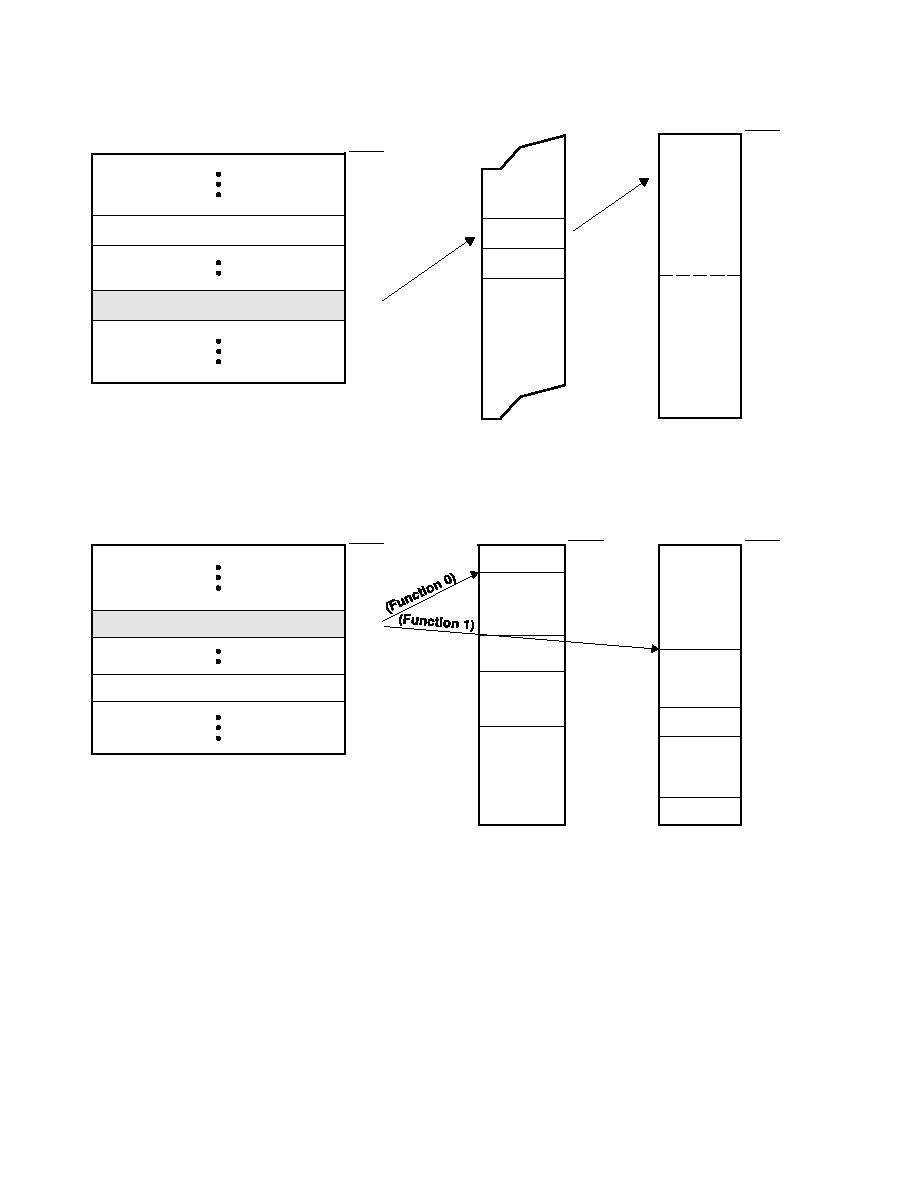
5≠2
16-Bit Legacy-Mode Base Address
PCI7x20 Configuration Registers
10h
CardBus Socket/ExCA Base Address
Note: The 16-bit legacy-mode base address
register is shared by function 0 and 1 as
indicated by the shading.
44h
Index
Data
Host I/O Space
PC Card A
ExCA
Registers
PC Card B
ExCA
Registers
00h
Offset
3Fh
40h
7Fh
Offset of desired register is placed in the index register and the
data from that location is returned in the data register.
Offset
Figure 5≠1. ExCA Register Access Through I/O
16-Bit Legacy-Mode Base Address
CardBus Socket/ExCA Base Address
10h
44h
CardBus
Socket A
Registers
ExCA
Registers
Card A
20h
800h
844h
Host
Memory Space
CardBus
Socket B
Registers
ExCA
Registers
Card B
20h
800h
844h
Host
Memory Space
Note: The CardBus socket/ExCA base
address mode register is separate for
functions 0 and 1.
address register's base address.
Offsets are from the CardBus socket/ExCA base
00h
00h
PCI7x20 Configuration Registers
Offset
Offset
Offset
Figure 5≠2. ExCA Register Access Through Memory

5≠3
Table 5≠1. ExCA Registers and Offsets
EXCA REGISTER NAME
PCI MEMORY ADDRESS
OFFSET (HEX)
EXCA OFFSET
(CARD A)
EXCA OFFSET
(CARD B)
Identification and revision
800
00
40
Interface status
801
01
41
Power control
802
02
42
Interrupt and general control
803
03
43
Card status change
804
04
44
Card status change interrupt configuration
805
05
45
Address window enable
806
06
46
I / O window control
807
07
47
I / O window 0 start-address low-byte
808
08
48
I / O window 0 start-address high-byte
809
09
49
I / O window 0 end-address low-byte
80A
0A
4A
I / O window 0 end-address high-byte
80B
0B
4B
I / O window 1 start-address low-byte
80C
0C
4C
I / O window 1 start-address high-byte
80D
0D
4D
I / O window 1 end-address low-byte
80E
0E
4E
I / O window 1 end-address high-byte
80F
0F
4F
Memory window 0 start-address low-byte
810
10
50
Memory window 0 start-address high-byte
811
11
51
Memory window 0 end-address low-byte
812
12
52
Memory window 0 end-address high-byte
813
13
53
Memory window 0 offset-address low-byte
814
14
54
Memory window 0 offset-address high-byte
815
15
55
Card detect and general control
816
16
56
Reserved
817
17
57
Memory window 1 start-address low-byte
818
18
58
Memory window 1 start-address high-byte
819
19
59
Memory window 1 end-address low-byte
81A
1A
5A
Memory window 1 end-address high-byte
81B
1B
5B
Memory window 1 offset-address low-byte
81C
1C
5C
Memory window 1 offset-address high-byte
81D
1D
5D
Global control
81E
1E
5E
Reserved
81F
1F
5F
Memory window 2 start-address low-byte
820
20
60
Memory window 2 start-address high-byte
821
21
61
Memory window 2 end-address low-byte
822
22
62
Memory window 2 end-address high-byte
823
23
63
Memory window 2 offset-address low-byte
824
24
64
Memory window 2 offset-address high-byte
825
25
65
One or more bits in this register are cleared only by the assertion of GRST when PME is enabled. If PME is not enabled, then this bit is cleared
by the assertion of PRST or GRST.
One or more bits in this register are cleared only by the assertion of GRST.

5≠4
Table 5≠1. ExCA Registers and Offsets (continued)
EXCA REGISTER NAME
PCI MEMORY ADDRESS
OFFSET (HEX)
EXCA OFFSET
(CARD A)
EXCA OFFSET
(CARD B)
Reserved
826
26
66
Reserved
827
27
67
Memory window 3 start-address low-byte
828
28
68
Memory window 3 start-address high-byte
829
29
69
Memory window 3 end-address low-byte
82A
2A
6A
Memory window 3 end-address high-byte
82B
2B
6B
Memory window 3 offset-address low-byte
82C
2C
6C
Memory window 3 offset-address high-byte
82D
2D
6D
Reserved
82E
2E
6E
Reserved
82F
2F
6F
Memory window 4 start-address low-byte
830
30
70
Memory window 4 start-address high-byte
831
31
71
Memory window 4 end-address low-byte
832
32
72
Memory window 4 end-address high-byte
833
33
73
Memory window 4 offset-address low-byte
834
34
74
Memory window 4 offset-address high-byte
835
35
75
I/O window 0 offset-address low-byte
836
36
76
I/O window 0 offset-address high-byte
837
37
77
I/O window 1 offset-address low-byte
838
38
78
I/O window 1 offset-address high-byte
839
39
79
Reserved
83A
3A
7A
Reserved
83B
3B
7B
Reserved
83C
3C
7C
Reserved
83D
3D
7D
Reserved
83E
3E
7E
Reserved
83F
3F
7F
Memory window page register 0
840
≠
≠
Memory window page register 1
841
≠
≠
Memory window page register 2
842
≠
≠
Memory window page register 3
843
≠
≠
Memory window page register 4
844
≠
≠

5≠5
5.1
ExCA Identification and Revision Register
This register provides host software with information on 16-bit PC Card support and 82365SL-DF compatibility. See
Table 5≠2 for a complete description of the register contents.
NOTE: If bit 5 (SUBSYRW) in the system control register is 1, then this register is read-only.
Bit
7
6
5
4
3
2
1
0
Name
ExCA identification and revision
Type
R
R
RW
RW
RW
RW
RW
RW
Default
1
0
0
0
0
1
0
0
Register:
ExCA identification and revision
Offset:
CardBus Socket Address + 800h:
Card A ExCA Offset 00h
Card B ExCA Offset 40h
Type:
Read/Write, Read-only
Default: 84h
Table 5≠2. ExCA Identification and Revision Register Description
BIT
SIGNAL
TYPE
FUNCTION
7≠6
IFTYPE
R
Interface type. These bits, which are hardwired as 10b, identify the 16-bit PC Card support provided by the
PCI7x20 device. The PCI7x20 device supports both I/O and memory 16-bit PC Cards.
5≠4
RSVD
RW
These bits can be used for 82365SL emulation.
3≠0
365REV
RW
82365SL-DF revision. This field stores the Intel 82365SL-DF revision supported by the PCI7x20 device. Host
software can read this field to determine compatibility to the 82365SL-DF register set. This field defaults to
0100b upon reset. Writing 0010b to this field places the controller in the 82356SL mode.
One or more bits in this register are cleared only by the assertion of GRST.
5≠6
5.2
ExCA Interface Status Register
This register provides information on current status of the PC Card interface. An X in the default bit values indicates
that the value of the bit after reset depends on the state of the PC Card interface. See Table 5≠3 for a complete
description of the register contents.
Bit
7
6
5
4
3
2
1
0
Name
ExCA interface status
Type
R
R
R
R
R
R
R
R
Default
0
0
X
X
X
X
X
X
Register:
ExCA interface status
Offset:
CardBus Socket Address + 801h:
Card A ExCA Offset 01h
Card B ExCA Offset 41h
Type:
Read-only
Default: 00XX XXXXb
Table 5≠3. ExCA Interface Status Register Description
BIT
SIGNAL
TYPE
FUNCTION
7
RSVD
R
This bit returns 0 when read. A write has no effect.
6
CARDPWR
R
CARDPWR. Card power. This bit indicates the current power status of the PC Card socket. This bit reflects
how the ExCA power control register has been programmed. The bit is encoded as:
0 = VCC and VPP to the socket are turned off (default).
1 = VCC and VPP to the socket are turned on.
5
READY
R
This bit indicates the current status of the READY signal at the PC Card interface.
0 = PC Card is not ready for a data transfer.
1 = PC Card is ready for a data transfer.
4
CARDWP
R
Card write protect. This bit indicates the current status of the WP signal at the PC Card interface. This signal
reports to the PCI7x20 device whether or not the memory card is write protected. Further, write protection
for an entire PCI7x20 16-bit memory window is available by setting the appropriate bit in the ExCA memory
window offset-address high-byte register.
0 = WP signal is 0. PC Card is R/W.
1 = WP signal is 1. PC Card is read-only.
3
CDETECT2
R
Card detect 2. This bit indicates the status of the CD2 signal at the PC Card interface. Software can use
this and CDETECT1 to determine if a PC Card is fully seated in the socket.
0 = CD2 signal is 1. No PC Card inserted.
1 = CD2 signal is 0. PC Card at least partially inserted.
2
CDETECT1
R
Card detect 1. This bit indicates the status of the CD1 signal at the PC Card interface. Software can use
this and CDETECT2 to determine if a PC Card is fully seated in the socket.
0 = CD1 signal is 1. No PC Card inserted.
1 = CD1 signal is 0. PC Card at least partially inserted.
1≠0
BVDSTAT
R
Battery voltage detect. When a 16-bit memory card is inserted, the field indicates the status of the battery
voltage detect signals (BVD1, BVD2) at the PC Card interface, where bit 0 reflects the BVD1 status, and
bit 1 reflects BVD2.
00 = Battery is dead.
01 = Battery is dead.
10 = Battery is low; warning.
11 = Battery is good.
When a 16-bit I/O card is inserted, this field indicates the status of the SPKR (bit 1) signal and the STSCHG
(bit 0) at the PC Card interface. In this case, the two bits in this field directly reflect the current state of these
card outputs.

5≠7
5.3
ExCA Power Control Register
This register provides PC Card power control. Bit 7 of this register enables the 16-bit outputs on the socket interface,
and can be used for power management in 16-bit PC Card applications. See Table 5≠5 for a complete description
of the register contents.
Bit
7
6
5
4
3
2
1
0
Name
ExCA power control
Type
RW
R
R
RW
RW
R
RW
RW
Default
0
0
0
0
0
0
0
0
Register:
ExCA power control
Offset:
CardBus Socket Address + 802h:
Card A ExCA Offset 02h
Card B ExCA Offset 42h
Type:
Read-only, Read/Write
Default: 00h
Table 5≠4. ExCA Power Control Register Description--82365SL Support
BIT
SIGNAL
TYPE
FUNCTION
7
COE
RW
Card output enable. Bit 7 controls the state of all of the 16-bit outputs on the PCI7x20 device. This bit is
encoded as:
0 = 16-bit PC Card outputs disabled (default)
1 = 16-bit PC Card outputs enabled
6
RSVD
R
Reserved. Bit 6 returns 0 when read.
5
AUTOPWRSWEN
RW
Auto power switch enable.
0 = Automatic socket power switching based on card detects is disabled.
1 = Automatic socket power switching based on card detects is enabled.
4
CAPWREN
RW
PC Card power enable.
0 = VCC = No connection
1 = VCC is enabled and controlled by bit 2 (EXCAPOWER) of the system control register
(PCI offset 80h, see Section 4.29).
3≠2
RSVD
R
Reserved. Bits 3 and 2 return 0s when read.
1≠0
EXCAVPP
RW
PC Card VPP power control. Bits 1 and 0 are used to request changes to card VPP. The PCI7x20 device
ignores this field unless VCC to the socket is enabled. This field is encoded as:
00 = No connection (default)
10 = 12 V
01 = VCC
11 = Reserved
One or more bits in this register are cleared only by the assertion of GRST when PME is enabled. If PME is not enabled, then this bit is cleared
by the assertion of PRST or GRST.
Table 5≠5. ExCA Power Control Register Description--82365SL-DF Support
BIT
SIGNAL
TYPE
FUNCTION
7
COE
RW
Card output enable. This bit controls the state of all of the 16-bit outputs on the PCI7x20 device. This bit
is encoded as:
0 = 16-bit PC Card outputs are disabled (default).
1 = 16-bit PC Card outputs are enabled.
6≠5
RSVD
R
Reserved. These bits return 0s when read. Writes have no effect.
4≠3
EXCAVCC
RW
VCC. These bits are used to request changes to card VCC. This field is encoded as:
00 = 0 V (default)
10 = 5 V
01 = 0 V reserved
11 = 3.3 V
2
RSVD
R
This bit returns 0 when read. A write has no effect.
1≠0
EXCAVPP
RW
VPP. These bits are used to request changes to card VPP. The PCI7x20 device ignores this field unless
VCC to the socket is enabled (i.e., 5 Vdc or 3.3 Vdc). This field is encoded as:
00 = 0 V (default)
10 = 12 V
01 = VCC
11 = 0 V reserved
This bit is cleared only by the assertion of GRST when PME is enabled. If PME is not enabled, then this bit is cleared by the assertion of PRST
or GRST.

5≠8
5.4
ExCA Interrupt and General Control Register
This register controls interrupt routing for I/O interrupts as well as other critical 16-bit PC Card functions. See
Table 5≠6 for a complete description of the register contents.
Bit
7
6
5
4
3
2
1
0
Name
ExCA interrupt and general control
Type
RW
RW
RW
RW
RW
RW
RW
RW
Default
0
0
0
0
0
0
0
0
Register:
ExCA interrupt and general control
Offset:
CardBus Socket Address + 803h:
Card A ExCA Offset 03h
Card B ExCA Offset 43h
Type:
Read/Write
Default: 00h
Table 5≠6. ExCA Interrupt and General Control Register Description
BIT
SIGNAL
TYPE
FUNCTION
7
RINGEN
RW
Card ring indicate enable. Enables the ring indicate function of the BVD1/RI terminals. This bit is encoded
as:
0 = Ring indicate disabled (default)
1 = Ring indicate enabled
6
RESET
RW
Card reset. This bit controls the 16-bit PC Card RESET signal, and allows host software to force a card
reset. This bit affects 16-bit cards only. This bit is encoded as:
0 = RESET signal asserted (default)
1 = RESET signal deasserted.
5
CARDTYPE
RW
Card type. This bit indicates the PC Card type. This bit is encoded as:
0 = Memory PC Card is installed (default)
1 = I/O PC Card is installed
4
CSCROUTE
RW
PCI interrupt ≠ CSC routing enable bit. This bit has meaning only if the CSC interrupt routing control bit
(PCI offset 93h, bit 5) is 0. In this case, when this bit is set (high), the card status change interrupts are
routed to PCI interrupts. When low, the card status change interrupts are routed using bits 7≠4 in the ExCA
card status-change interrupt configuration register (ExCA offset 805h, see Section 5.6). This bit is encoded
as:
0 = CSC interrupts routed by ExCA registers (default)
1 = CSC interrupts routed to PCI interrupts
If the CSC interrupt routing control bit (bit 5) of the diagnostic register (PCI offset 93h, see Section 4.40)
is set to 1, this bit has no meaning, which is the default case.
3≠0
INTSELECT
RW
Card interrupt select for I/O PC Card functional interrupts. These bits select the interrupt routing for I/O
PC Card functional interrupts. This field is encoded as:
0000 = No IRQ selected (default). CSC interrupts are routed to PCI Interrupts. This bit setting is ORed
with bit 4 (CSCROUTE) for backward compatibility.
0001 = IRQ1 enabled
0010 = SMI enabled
0011 = IRQ3 enabled
0100 = IRQ4 enabled
0101 = IRQ5 enabled
0110 = IRQ6 enabled
0111 = IRQ7 enabled
1000 = IRQ8 enabled
1001 = IRQ9 enabled
1010 = IRQ10 enabled
1011 = IRQ11 enabled
1100 = IRQ12 enabled
1101 = IRQ13 enabled
1110 = IRQ14 enabled
1111 = IRQ15 enabled
This bit is cleared only by the assertion of GRST when PME is enabled. If PME is not enabled, then this bit is cleared by the assertion of PRST
or GRST.
5≠9
5.5
ExCA Card Status-Change Register
The ExCA card status-change register controls interrupt routing for I/O interrupts as well as other critical 16-bit PC
Card functions. The register enables these interrupt sources to generate an interrupt to the host. When the interrupt
source is disabled, the corresponding bit in this register always reads 0. When an interrupt source is enabled, the
corresponding bit in this register is set to indicate that the interrupt source is active. After generating the interrupt to
the host, the interrupt service routine must read this register to determine the source of the interrupt. The interrupt
service routine is responsible for resetting the bits in this register as well. Resetting a bit is accomplished by one of
two methods: a read of this register or an explicit writeback of 1 to the status bit. The choice of these two methods
is based on bit 2 (interrupt flag clear mode select) in the ExCA global control register (CB offset 81Eh, see
Section 5.20). See Table 5≠7 for a complete description of the register contents.
Bit
7
6
5
4
3
2
1
0
Name
ExCA card status-change
Type
R
R
R
R
R
R
R
R
Default
0
0
0
0
0
0
0
0
Register:
ExCA card status-change
Type:
Read-only
Offset:
CardBus socket address + 804h; Card A ExCA offset 04h
Card B ExCA offset 44h
Default:
00h
Table 5≠7. ExCA Card Status-Change Register Description
BIT
SIGNAL
TYPE
FUNCTION
7≠4
RSVD
R
Reserved. Bits 7≠4 return 0s when read.
3
CDCHANGE
R
Card detect change. Bit 3 indicates whether a change on CD1 or CD2 occurred at the PC Card
interface. This bit is encoded as:
0 = No change detected on either CD1 or CD2
1 = Change detected on either CD1 or CD2
2
READYCHANGE
R
Ready change. When a 16-bit memory is installed in the socket, bit 2 includes whether the source of
a PCI7x20 interrupt was due to a change on READY at the PC Card interface, indicating that the
PC Card is now ready to accept new data. This bit is encoded as:
0 = No low-to-high transition detected on READY (default)
1 = Detected low-to-high transition on READY
When a 16-bit I/O card is installed, bit 2 is always 0.
1
BATWARN
R
Battery warning change. When a 16-bit memory card is installed in the socket, bit 1 indicates whether
the source of a PCI7x20 interrupt was due to a battery-low warning condition. This bit is encoded as:
0 = No battery warning condition (default)
1 = Detected battery warning condition
When a 16-bit I/O card is installed, bit 1 is always 0.
0
BATDEAD
R
Battery dead or status change. When a 16-bit memory card is installed in the socket, bit 0 indicates
whether the source of a PCI7x20 interrupt was due to a battery dead condition. This bit is encoded as:
0 = STSCHG deasserted (default)
1 = STSCHG asserted
Ring indicate. When the PCI7x20 is configured for ring indicate operation, bit 0 indicates the status of
RI.
These are PME context bits and can be cleared only by the assertion of GRST when PME is enabled. If PME is not enabled, then these bits are
cleared by the assertion of PRST or GRST.

5≠10
5.6
ExCA Card Status-Change Interrupt Configuration Register
This register controls interrupt routing for CSC interrupts, as well as masks/unmasks CSC interrupt sources. See
Table 5≠8 for a complete description of the register contents.
Bit
7
6
5
4
3
2
1
0
Name
ExCA card status-change interrupt configuration
Type
RW
RW
RW
RW
RW
RW
RW
RW
Default
0
0
0
0
0
0
0
0
Register:
ExCA card status-change interrupt configuration
Offset:
CardBus Socket Address + 805h:
Card A ExCA Offset 05h
Card B ExCA Offset 45h
Type:
Read/Write
Default: 00h
Table 5≠8. ExCA Card Status-Change Interrupt Configuration Register Description
BIT
SIGNAL
TYPE
FUNCTION
7≠4
CSCSELECT
RW
Interrupt select for card status change. These bits select the interrupt routing for card status-change
interrupts. This field is encoded as:
0000 = CSC interrupts routed to PCI interrupts if bit 5 of the diagnostic register (PCI offset 93h) is set
to 1b. In this case bit 4 of ExCA 803 is a don't care. This is the default setting.
0000 = No ISA interrupt routing if bit 5 of the diagnostic register (PCI offset 93h) is set to 0b. In this case,
CSC interrupts are routed to PCI interrupts by setting bit 4 of ExCA 803h to 1b.
0001 = IRQ1 enabled
0010 = SMI enabled
0011 = IRQ3 enabled
0100 = IRQ4 enabled
0101 = IRQ5 enabled
0110 = IRQ6 enabled
0111 = IRQ7 enabled
1000 = IRQ8 enabled
1001 = IRQ9 enabled
1010 = IRQ10 enabled
1011 = IRQ11 enabled
1100 = IRQ12 enabled
1101 = IRQ13 enabled
1110 = IRQ14 enabled
1111 = IRQ15 enabled
3
CDEN
RW
Card detect enable. Enables interrupts on CD1 or CD2 changes. This bit is encoded as:
0 = Disables interrupts on CD1 or CD2 line changes (default)
1 = Enables interrupts on CD1 or CD2 line changes
2
READYEN
RW
Ready enable. This bit enables/disables a low-to-high transition on the PC Card READY signal to generate
a host interrupt. This interrupt source is considered a card status change. This bit is encoded as:
0 = Disables host interrupt generation (default)
1 = Enables host interrupt generation
1
BATWARNEN
RW
Battery warning enable. This bit enables/disables a battery warning condition to generate a CSC interrupt.
This bit is encoded as:
0 = Disables host interrupt generation (default)
1 = Enables host interrupt generation
0
BATDEADEN
RW
Battery dead enable. This bit enables/disables a battery dead condition on a memory PC Card or assertion
of the STSCHG I/O PC Card signal to generate a CSC interrupt.
0 = Disables host interrupt generation (default)
1 = Enables host interrupt generation
This bit is cleared only by the assertion of GRST when PME is enabled. If PME is not enabled, then this bit is cleared by the assertion of PRST
or GRST.

5≠11
5.7
ExCA Address Window Enable Register
The ExCA address window enable register enables/disables the memory and I/O windows to the 16-bit PC Card. By
default, all windows to the card are disabled. The PCI7x20 device does not acknowledge PCI memory or I/O cycles
to the card if the corresponding enable bit in this register is 0, regardless of the programming of the memory or I/O
window start/end/offset address registers. See Table 5≠9 for a complete description of the register contents.
Bit
7
6
5
4
3
2
1
0
Name
ExCA address window enable
Type
RW
RW
R
RW
RW
RW
RW
RW
Default
0
0
0
0
0
0
0
0
Register:
ExCA address window enable
Type:
Read-only, Read/Write
Offset:
CardBus socket address + 806h; Card A ExCA offset 06h
Card B ExCA offset 46h
Default:
00h
Table 5≠9. ExCA Address Window Enable Register Description
BIT
SIGNAL
TYPE
FUNCTION
7
IOWIN1EN
RW
I/O window 1 enable. Bit 7 enables/disables I/O window 1 for the PC Card. This bit is encoded as:
0 = I/O window 1 disabled (default)
1 = I/O window 1 enabled
6
IOWIN0EN
RW
I/O window 0 enable. Bit 6 enables/disables I/O window 0 for the PC Card. This bit is encoded as:
0 = I/O window 0 disabled (default)
1 = I/O window 0 enabled
5
RSVD
R
Reserved. Bit 5 returns 0 when read.
4
MEMWIN4EN
RW
Memory window 4 enable. Bit 4 enables/disables memory window 4 for the PC Card. This bit is
encoded as:
0 = Memory window 4 disabled (default)
1 = Memory window 4 enabled
3
MEMWIN3EN
RW
Memory window 3 enable. Bit 3 enables/disables memory window 3 for the PC Card. This bit is
encoded as:
0 = Memory window 3 disabled (default)
1 = Memory window 3 enabled
2
MEMWIN2EN
RW
Memory window 2 enable. Bit 2 enables/disables memory window 2 for the PC Card. This bit is
encoded as:
0 = Memory window 2 disabled (default)
1 = Memory window 2 enabled
1
MEMWIN1EN
RW
Memory window 1 enable. Bit 1 enables/disables memory window 1 for the PC Card. This bit is
encoded as:
0 = Memory window 1 disabled (default)
1 = Memory window 1 enabled
0
MEMWIN0EN
RW
Memory window 0 enable. Bit 0 enables/disables memory window 0 for the PC Card. This bit is
encoded as:
0 = Memory window 0 disabled (default)
1 = Memory window 0 enabled

5≠12
5.8
ExCA I/O Window Control Register
The ExCA I/O window control register contains parameters related to I/O window sizing and cycle timing. See
Table 5≠10 for a complete description of the register contents.
Bit
7
6
5
4
3
2
1
0
Name
ExCA I/O window control
Type
RW
RW
RW
RW
RW
RW
RW
RW
Default
0
0
0
0
0
0
0
0
Register:
ExCA
I
/O window control
Type:
Read/Write
Offset:
CardBus socket address + 807h: Card A ExCA offset 07h
Card B ExCA offset 47h
Default:
00h
Table 5≠10. ExCA I/O Window Control Register Description
BIT
SIGNAL
TYPE
FUNCTION
7
WAITSTATE1
RW
I/O window 1 wait state. Bit 7 controls the I/O window 1 wait state for 16-bit I/O accesses. Bit 7 has no effect
on 8-bit accesses. This wait-state timing emulates the ISA wait state used by the Intel
82365SL-DF. This
bit is encoded as:
0 = 16-bit cycles have standard length (default).
1 = 16-bit cycles are extended by one equivalent ISA wait state.
6
ZEROWS1
RW
I/O window 1 zero wait state. Bit 6 controls the I/O window 1 wait state for 8-bit I/O accesses. Bit 6 has
no effect on 16-bit accesses. This wait-state timing emulates the ISA wait state used by the Intel
82365SL-DF. This bit is encoded as:
0 = 8-bit cycles have standard length (default).
1 = 8-bit cycles are reduced to equivalent of three ISA cycles.
5
IOSIS16W1
RW
I/O window 1 IOIS16 source. Bit 5 controls the I/O window 1 automatic data-sizing feature that uses IOIS16
from the PC Card to determine the data width of the I/O data transfer. This bit is encoded as:
0 = Window data width determined by DATASIZE1, bit 4 (default).
1 = Window data width determined by IOIS16.
4
DATASIZE1
RW
I/O window 1 data size. Bit 4 controls the I/O window 1 data size. Bit 4 is ignored if bit 5 (IOSIS16W1) is
set. This bit is encoded as:
0 = Window data width is 8 bits (default).
1 = Window data width is 16 bits.
3
WAITSTATE0
RW
I/O window 0 wait state. Bit 3 controls the I/O window 0 wait state for 16-bit I/O accesses. Bit 3 has no effect
on 8-bit accesses. This wait-state timing emulates the ISA wait state used by the Intel
82365SL-DF. This
bit is encoded as:
0 = 16-bit cycles have standard length (default).
1 = 16-bit cycles are extended by one equivalent ISA wait state.
2
ZEROWS0
RW
I/O window 0 zero wait state. Bit 2 controls the I/O window 0 wait state for 8-bit I/O accesses. Bit 2 has
no effect on 16-bit accesses. This wait-state timing emulates the ISA wait state used by the Intel
82365SL-DF. This bit is encoded as:
0 = 8-bit cycles have standard length (default).
1 = 8-bit cycles are reduced to equivalent of three ISA cycles.
1
IOSIS16W0
RW
I/O window 0 IOIS16 source. Bit 1 controls the I/O window 0 automatic data sizing feature that uses IOIS16
from the PC Card to determine the data width of the I/O data transfer. This bit is encoded as:
0 = Window data width is determined by DATASIZE0, bit 0 (default).
1 = Window data width is determined by IOIS16.
0
DATASIZE0
RW
I/O window 0 data size. Bit 0 controls the I/O window 0 data size. Bit 0 is ignored if bit 1 (IOSIS16W0) is
set. This bit is encoded as:
0 = Window data width is 8 bits (default).
1 = Window data width is 16 bits.

5≠13
5.9
ExCA I/O Windows 0 and 1 Start-Address Low-Byte Registers
These registers contain the low byte of the 16-bit I/O window start address for I/O windows 0 and 1. The 8 bits of these
registers correspond to the lower 8 bits of the start address.
Bit
7
6
5
4
3
2
1
0
Name
ExCA I/O windows 0 and 1 start-address low-byte
Type
RW
RW
RW
RW
RW
RW
RW
RW
Default
0
0
0
0
0
0
0
0
Register:
ExCA I/O window 0 start-address low-byte
Offset:
CardBus Socket Address + 808h:
Card A ExCA Offset 08h
Card B ExCA Offset 48h
Register:
ExCA I/O window 1 start-address low-byte
Offset:
CardBus Socket Address + 80Ch:
Card A ExCA Offset 0Ch
Card B ExCA Offset 4Ch
Type:
Read/Write
Default: 00h
5.10 ExCA I/O Windows 0 and 1 Start-Address High-Byte Registers
These registers contain the high byte of the 16-bit I/O window start address for I/O windows 0 and 1. The 8 bits of
these registers correspond to the upper 8 bits of the start address.
Bit
7
6
5
4
3
2
1
0
Name
ExCA I/O windows 0 and 1 start-address high-byte
Type
RW
RW
RW
RW
RW
RW
RW
RW
Default
0
0
0
0
0
0
0
0
Register:
ExCA I/O window 0 start-address high-byte
Offset:
CardBus Socket Address + 809h:
Card A ExCA Offset 09h
Card B ExCA Offset 49h
Register:
ExCA I/O window 1 start-address high-byte
Offset:
CardBus Socket Address + 80Dh:
Card A ExCA Offset 0Dh
Card B ExCA Offset 4Dh
Type:
Read/Write
Default: 00h

5≠14
5.11 ExCA I/O Windows 0 and 1 End-Address Low-Byte Registers
These registers contain the low byte of the 16-bit I/O window end address for I/O windows 0 and 1. The 8 bits of these
registers correspond to the lower 8 bits of the start address.
Bit
7
6
5
4
3
2
1
0
Name
ExCA I/O windows 0 and 1 end-address low-byte
Type
RW
RW
RW
RW
RW
RW
RW
RW
Default
0
0
0
0
0
0
0
0
Register:
ExCA I/O window 0 end-address low-byte
Offset:
CardBus Socket Address + 80Ah:
Card A ExCA Offset 0Ah
Card B ExCA Offset 4Ah
Register:
ExCA I/O window 1 end-address low-byte
Offset:
CardBus Socket Address + 80Eh:
Card A ExCA Offset 0Eh
Card B ExCA Offset 4Eh
Type:
Read/Write
Default: 00h
5.12 ExCA I/O Windows 0 and 1 End-Address High-Byte Registers
These registers contain the high byte of the 16-bit I/O window end address for I/O windows 0 and 1. The 8 bits of these
registers correspond to the upper 8 bits of the end address.
Bit
7
6
5
4
3
2
1
0
Name
ExCA I/O windows 0 and 1 end-address high-byte
Type
RW
RW
RW
RW
RW
RW
RW
RW
Default
0
0
0
0
0
0
0
0
Register:
ExCA I/O window 0 end-address high-byte
Offset:
CardBus Socket Address + 80Bh:
Card A ExCA Offset 0Bh
Card B ExCA Offset 4Bh
Register:
ExCA I/O window 1 end-address high-byte
Offset:
CardBus Socket Address + 80Fh:
Card A ExCA Offset 0Fh
Card B ExCA Offset 4Fh
Type:
Read/Write
Default:
00h

5≠15
5.13 ExCA Memory Windows 0≠4 Start-Address Low-Byte Registers
These registers contain the low byte of the 16-bit memory window start address for memory windows 0, 1, 2, 3, and 4.
The 8 bits of these registers correspond to bits A19≠A12 of the start address.
Bit
7
6
5
4
3
2
1
0
Name
ExCA memory windows 0≠4 start-address low-byte
Type
RW
RW
RW
RW
RW
RW
RW
RW
Default
0
0
0
0
0
0
0
0
Register:
ExCA memory window 0 start-address low-byte
Offset:
CardBus Socket Address + 810h:
Card A ExCA Offset 10h
Card B ExCA Offset 50h
Register:
ExCA memory window 1 start-address low-byte
Offset:
CardBus Socket Address + 818h:
Card A ExCA Offset 18h
Card B ExCA Offset 58h
Register:
ExCA memory window 2 start-address low-byte
Offset:
CardBus Socket Address + 820h:
Card A ExCA Offset 20h
Card B ExCA Offset 60h
Register:
ExCA memory window 3 start-address low-byte
Offset:
CardBus Socket Address + 828h:
Card A ExCA Offset 28h
Card B ExCA Offset 68h
Register:
ExCA memory window 4 start-address low-byte
Offset:
CardBus Socket Address + 830h:
Card A ExCA Offset 30h
Card B ExCA Offset 70h
Type:
Read/Write
Default: 00h

5≠16
5.14 ExCA Memory Windows 0≠4 Start-Address High-Byte Registers
These registers contain the high nibble of the 16-bit memory window start address for memory windows 0, 1, 2, 3,
and 4. The lower 4 bits of these registers correspond to bits A23≠A20 of the start address. In addition, the memory
window data width and wait states are set in this register. See Table 5≠11 for a complete description of the register
contents.
Bit
7
6
5
4
3
2
1
0
Name
ExCA memory windows 0≠4 start-address high-byte
Type
RW
RW
RW
RW
RW
RW
RW
RW
Default
0
0
0
0
0
0
0
0
Register:
ExCA memory window 0 start-address high-byte
Offset:
CardBus Socket Address + 811h:
Card A ExCA Offset 11h
Card B ExCA Offset 51h
Register:
ExCA memory window 1 start-address high-byte
Offset:
CardBus Socket Address + 819h:
Card A ExCA Offset 19h
Card B ExCA Offset 59h
Register:
ExCA memory window 2 start-address high-byte
Offset:
CardBus Socket Address + 821h:
Card A ExCA Offset 21h
Card B ExCA Offset 61h
Register:
ExCA memory window 3 start-address high-byte
Offset:
CardBus Socket Address + 829h:
Card A ExCA Offset 29h
Card B ExCA Offset 69h
Register:
ExCA memory window 4 start-address high-byte
Offset:
CardBus Socket Address + 831h:
Card A ExCA Offset 31h
Card B ExCA Offset 71h
Type:
Read/Write
Default: 00h
Table 5≠11. ExCA Memory Windows 0≠4 Start-Address High-Byte Registers Description
BIT
SIGNAL
TYPE
FUNCTION
7
DATASIZE
RW
This bit controls the memory window data width. This bit is encoded as:
0 = Window data width is 8 bits (default)
1 = Window data width is 16 bits
6
ZEROWAIT
RW
Zero wait-state. This bit controls the memory window wait state for 8- and 16-bit accesses. This wait-state
timing emulates the ISA wait state used by the 82365SL-DF. This bit is encoded as:
0 = 8- and 16-bit cycles have standard length (default).
1 = 8-bit cycles reduced to equivalent of three ISA cycles
16-bit cycles reduced to the equivalent of two ISA cycles
5≠4
SCRATCH
RW
Scratch pad bits. These bits have no effect on memory window operation.
3≠0
STAHN
RW
Start address high-nibble. These bits represent the upper address bits A23≠A20 of the memory window
start address.

5≠17
5.15 ExCA Memory Windows 0≠4 End-Address Low-Byte Registers
These registers contain the low byte of the 16-bit memory window end address for memory windows 0, 1, 2, 3, and 4.
The 8 bits of these registers correspond to bits A19≠A12 of the end address.
Bit
7
6
5
4
3
2
1
0
Name
ExCA memory windows 0≠4 end-address low-byte
Type
RW
RW
RW
RW
RW
RW
RW
RW
Default
0
0
0
0
0
0
0
0
Register:
ExCA memory window 0 end-address low-byte
Offset:
CardBus Socket Address + 812h:
Card A ExCA Offset 12h
Card B ExCA Offset 52h
Register:
ExCA memory window 1 end-address low-byte
Offset:
CardBus Socket Address + 81Ah:
Card A ExCA Offset 1Ah
Card B ExCA Offset 5Ah
Register:
ExCA memory window 2 end-address low-byte
Offset:
CardBus Socket Address + 822h:
Card A ExCA Offset 22h
Card B ExCA Offset 62h
Register:
ExCA memory window 3 end-address low-byte
Offset:
CardBus Socket Address + 82Ah:
Card A ExCA Offset 2Ah
Card B ExCA Offset 6Ah
Register:
ExCA memory window 4 end-address low-byte
Offset:
CardBus Socket Address + 832h:
Card A ExCA Offset 32h
Card B ExCA Offset 72h
Type:
Read/Write
Default: 00h

5≠18
5.16 ExCA Memory Windows 0≠4 End-Address High-Byte Registers
These registers contain the high nibble of the 16-bit memory window end address for memory windows 0, 1, 2, 3,
and 4. The lower 4 bits of these registers correspond to bits A23≠A20 of the end address. In addition, the memory
window wait states are set in this register. See Table 5≠12 for a complete description of the register contents.
Bit
7
6
5
4
3
2
1
0
Name
ExCA memory windows 0≠4 end-address high-byte
Type
RW
RW
R
R
RW
RW
RW
RW
Default
0
0
0
0
0
0
0
0
Register:
ExCA memory window 0 end-address high-byte
Offset:
CardBus Socket Address + 813h:
Card A ExCA Offset 13h
Card B ExCA Offset 53h
Register:
ExCA memory window 1 end-address high-byte
Offset:
CardBus Socket Address + 81Bh:
Card A ExCA Offset 1Bh
Card B ExCA Offset 5Bh
Register:
ExCA memory window 2 end-address high-byte
Offset:
CardBus Socket Address + 823h:
Card A ExCA Offset 23h
Card B ExCA Offset 63h
Register:
ExCA memory window 3 end-address high-byte
Offset:
CardBus Socket Address + 82Bh:
Card A ExCA Offset 2Bh
Card B ExCA Offset 6Bh
Register:
ExCA Memory window 4 end-address high-byte
Offset:
CardBus Socket Address + 833h:
Card A ExCA Offset 33h
Card B ExCA Offset 73h
Type:
Read/Write, Read-only
Default: 00h
Table 5≠12. ExCA Memory Windows 0≠4 End-Address High-Byte Registers Description
BIT
SIGNAL
TYPE
FUNCTION
7≠6
MEMWS
RW
Wait state. These bits specify the number of equivalent ISA wait states to be added to 16-bit memory
accesses. The number of wait states added is equal to the binary value of these 2 bits.
5≠4
RSVD
R
Reserved. These bits return 0s when read. Writes have no effect.
3≠0
ENDHN
RW
End-address high nibble. These bits represent the upper address bits A23≠A20 of the memory window end
address.

5≠19
5.17 ExCA Memory Windows 0≠4 Offset-Address Low-Byte Registers
These registers contain the low byte of the 16-bit memory window offset address for memory windows 0, 1, 2, 3,
and 4. The 8 bits of these registers correspond to bits A19≠A12 of the offset address.
Bit
7
6
5
4
3
2
1
0
Name
ExCA memory windows 0≠4 offset-address low-byte
Type
RW
RW
RW
RW
RW
RW
RW
RW
Default
0
0
0
0
0
0
0
0
Register:
ExCA memory window 0 offset-address low-byte
Offset:
CardBus Socket Address + 814h:
Card A ExCA Offset 14h
Card B ExCA Offset 54h
Register:
ExCA memory window 1 offset-address low-byte
Offset:
CardBus Socket Address + 81Ch:
Card A ExCA Offset 1Ch
Card B ExCA Offset 5Ch
Register:
ExCA memory window 2 offset-address low-byte
Offset:
CardBus Socket Address + 824h:
Card A ExCA Offset 24h
Card B ExCA Offset 64h
Register:
ExCA memory window 3 offset-address low-byte
Offset:
CardBus Socket Address + 82Ch:
Card A ExCA Offset 2Ch
Card B ExCA Offset 6Ch
Register:
ExCA memory window 4 offset-address low-byte
Offset:
CardBus Socket Address + 834h:
Card A ExCA Offset 34h
Card B ExCA Offset 74h
Type:
Read/Write
Default: 00h

5≠20
5.18 ExCA Memory Windows 0≠4 Offset-Address High-Byte Registers
These registers contain the high 6 bits of the 16-bit memory window offset address for memory windows 0, 1, 2, 3,
and 4. The lower 6 bits of these registers correspond to bits A25≠A20 of the offset address. In addition, the write
protection and common/attribute memory configurations are set in this register. See Table 5≠13 for a complete
description of the register contents.
Bit
7
6
5
4
3
2
1
0
Name
ExCA memory window 0≠4 offset-address high-byte
Type
RW
RW
RW
RW
RW
RW
RW
RW
Default
0
0
0
0
0
0
0
0
Register:
ExCA memory window 0 offset-address high-byte
Offset:
CardBus Socket Address + 815h:
Card A ExCA Offset 15h
Card B ExCA Offset 55h
Register:
ExCA memory window 1 offset-address high-byte
Offset:
CardBus Socket Address + 81Dh:
Card A ExCA Offset 1Dh
Card B ExCA Offset 5Dh
Register:
ExCA memory window 2 offset-address high-byte
Offset:
CardBus Socket Address + 825h:
Card A ExCA Offset 25h
Card B ExCA Offset 65h
Register:
ExCA memory window 3 offset-address high-byte
Offset:
CardBus Socket Address + 82Dh:
Card A ExCA Offset 2Dh
Card B ExCA Offset 6Dh
Register:
ExCA memory window 4 offset-address high-byte
Offset:
CardBus Socket Address + 835h:
Card A ExCA Offset 35h
Card B ExCA Offset 75h
Type:
Read/Write
Default: 00h
Table 5≠13. ExCA Memory Windows 0≠4 Offset-Address High-Byte Registers Description
BIT
SIGNAL
TYPE
FUNCTION
7
WINWP
RW
Write protect. This bit specifies whether write operations to this memory window are enabled.
This bit is encoded as:
0 = Write operations are allowed (default).
1 = Write operations are not allowed.
6
REG
RW
This bit specifies whether this memory window is mapped to card attribute or common memory.
This bit is encoded as:
0 = Memory window is mapped to common memory (default).
1 = Memory window is mapped to attribute memory.
5≠0
OFFHB
RW
Offset-address high byte. These bits represent the upper address bits A25≠A20 of the memory window offset
address.

5≠21
5.19 ExCA Card Detect and General Control Register
This register controls how the ExCA registers for the socket respond to card removal. It also reports the status of the
VS1 and VS2 signals at the PC Card interface. Table 5≠14 describes each bit in the ExCA card detect and general
control register.
Bit
7
6
5
4
3
2
1
0
Name
ExCA card detect and general control
Type
R
R
W
RW
R
R
RW
R
Default
X
X
0
0
0
0
0
0
Register:
ExCA card detect and general control
Offset:
CardBus Socket Address + 816h:
Card A ExCA Offset 16h
Card B ExCA Offset 56h
Type:
Read-only, Write-only, Read/Write
Default: XX00 0000b
Table 5≠14. ExCA Card Detect and General Control Register Description
BIT
SIGNAL
TYPE
FUNCTION
7
VS2STAT
R
VS2. This bit reports the current state of the VS2 signal at the PC Card interface, and, therefore, does not
have a default value.
0 = VS2 is low.
1 = VS2 is high.
6
VS1STAT
R
VS1. This bit reports the current state of the VS1 signal at the PC Card interface, and, therefore, does not
have a default value.
0 = VS1 is low.
1 = VS1 is high.
5
SWCSC
W
Software card detect interrupt. If card detect enable, bit 3 in the ExCA card status change interrupt
configuration register (ExCA offset 805h, see Section 5.6) is set, then writing a 1 to this bit causes a
card-detect card-status-change interrupt for the associated card socket.
If the card-detect enable bit is cleared to 0 in the ExCA card status-change interrupt configuration register
(ExCA offset 805h, see Section 5.6), then writing a 1 to the software card-detect interrupt bit has no effect.
This bit is write-only.
A read operation of this bit always returns 0. Writing a 1 to this bit also clears it. If bit 2 of the ExCA global
control register (ExCA offset 81Eh, see Section 5.20) is set and a 1 is written to clear bit 3 of the ExCA
card status change interrupt register, then this bit also is cleared.
4
CDRESUME
RW
Card detect resume enable. If this bit is set to 1 and a card detect change has been detected on the CD1
and CD2 inputs, then the RI_OUT output goes from high to low. The RI_OUT remains low until the card
status change bit in the ExCA card status-change register (ExCA offset 804h, see Section 5.5) is cleared.
If this bit is a 0, then the card detect resume functionality is disabled.
0 = Card detect resume disabled (default)
1 = Card detect resume enabled
3≠2
RSVD
R
These bits return 0s when read. Writes have no effect.
1
REGCONFIG
RW
Register configuration upon card removal. This bit controls how the ExCA registers for the socket react
to a card removal event. This bit is encoded as:
0 = No change to ExCA registers upon card removal (default)
1 = Reset ExCA registers upon card removal
0
RSVD
R
This bit returns 0 when read. A write has no effect.
One or more bits in this register are cleared only by the assertion of GRST when PME is enabled. If PME is not enabled, then this bit is cleared
by the assertion of PRST or GRST.

5≠22
5.20 ExCA Global Control Register
This register controls both PC Card sockets, and is not duplicated for each socket. The host interrupt mode bits in
this register are retained for 82365SL-DF compatibility. See Table 5≠15 for a complete description of the register
contents.
Bit
7
6
5
4
3
2
1
0
Name
ExCA global control
Type
R
R
R
RW
RW
RW
RW
RW
Default
0
0
0
0
0
0
0
0
Register:
ExCA global control
Offset:
CardBus Socket Address + 81Eh:
Card A ExCA Offset 1Eh
Card B ExCA Offset 5Eh
Type:
Read-only, Read/Write
Default: 00h
Table 5≠15. ExCA Global Control Register Description
BIT
SIGNAL
TYPE
FUNCTION
7≠5
RSVD
R
These bits return 0s when read. Writes have no effect.
4
INTMODEB
RW
Level/edge interrupt mode select, card B. This bit selects the signaling mode for the PCI7x20 host interrupt
for card B interrupts. This bit is encoded as:
0 = Host interrupt is edge mode (default).
1 = Host interrupt is level mode.
3
INTMODEA
RW
Level/edge interrupt mode select, card A. This bit selects the signaling mode for the PCI7x20 host interrupt
for card A interrupts. This bit is encoded as:
0 = Host interrupt is edge-mode (default).
1 = Host interrupt is level-mode.
2
IFCMODE
RW
Interrupt flag clear mode select. This bit selects the interrupt flag clear mechanism for the flags in the ExCA
card status change register. This bit is encoded as:
0 = Interrupt flags cleared by read of CSC register (default)
1 = Interrupt flags cleared by explicit writeback of 1
1
CSCMODE
RW
Card status change level/edge mode select. This bit selects the signaling mode for the PCI7x20 host
interrupt for card status changes. This bit is encoded as:
0 = Host interrupt is edge-mode (default).
1 = Host interrupt is level-mode.
0
PWRDWN
RW
Power-down mode select. When this bit is set to 1, the PCI7x20 device is in power-down mode. In
power-down mode the PCI7x20 card outputs are placed in a high-impedance state until an active cycle
is executed on the card interface. Following an active cycle the outputs are again placed in a
high-impedance state. The PCI7x20 device still receives functional interrupts and/or card status change
interrupts; however, an actual card access is required to wake up the interface. This bit is encoded as:
0 = Power-down mode disabled (default)
1 = Power-down mode enabled
One or more bits in this register are cleared only by the assertion of GRST.

5≠23
5.21 ExCA I/O Windows 0 and 1 Offset-Address Low-Byte Registers
These registers contain the low byte of the 16-bit I/O window offset address for I/O windows 0 and 1. The 8 bits of
these registers correspond to the lower 8 bits of the offset address, and bit 0 is always 0.
Bit
7
6
5
4
3
2
1
0
Name
ExCA I/O windows 0 and 1 offset-address low-byte
Type
RW
RW
RW
RW
RW
RW
RW
R
Default
0
0
0
0
0
0
0
0
Register:
ExCA I/O window 0 offset-address low-byte
Offset:
CardBus Socket Address + 836h:
Card A ExCA Offset 36h
Card B ExCA Offset 76h
Register:
ExCA I/O window 1 offset-address low-byte
Offset:
CardBus Socket Address + 838h:
Card A ExCA Offset 38h
Card B ExCA Offset 78h
Type:
Read/Write, Read-only
Default: 00h
5.22 ExCA I/O Windows 0 and 1 Offset-Address High-Byte Registers
These registers contain the high byte of the 16-bit I/O window offset address for I/O windows 0 and 1. The 8 bits of
these registers correspond to the upper 8 bits of the offset address.
Bit
7
6
5
4
3
2
1
0
Name
ExCA I/O windows 0 and 1 offset-address high-byte
Type
RW
RW
RW
RW
RW
RW
RW
RW
Default
0
0
0
0
0
0
0
0
Register:
ExCA I/O window 0 offset-address high-byte
Offset:
CardBus Socket Address + 837h:
Card A ExCA Offset 37h
Card B ExCA Offset 77h
Register:
ExCA I/O window 1 offset-address high-byte
Offset:
CardBus Socket Address + 839h:
Card A ExCA Offset 39h
Card B ExCA Offset 79h
Type:
Read/Write
Default: 00h

5≠24
5.23 ExCA Memory Windows 0≠4 Page Registers
The upper 8 bits of a 4-byte PCI memory address are compared to the contents of this register when decoding
addresses for 16-bit memory windows. Each window has its own page register, all of which default to 00h. By
programming this register to a nonzero value, host software can locate 16-bit memory windows in any one of 256
16-Mbyte regions in the 4-gigabyte PCI address space. These registers are only accessible when the ExCA registers
are memory-mapped, that is, these registers may not be accessed using the index/data I/O scheme.
Bit
7
6
5
4
3
2
1
0
Name
ExCA memory windows 0≠4 page
Type
RW
RW
RW
RW
RW
RW
RW
R
Default
0
0
0
0
0
0
0
0
Register:
ExCA memory windows 0≠4 page
Offset:
CardBus Socket Address + 840h, 841h, 842h, 843h, 844h
Type:
Read/Write
Default: 00h
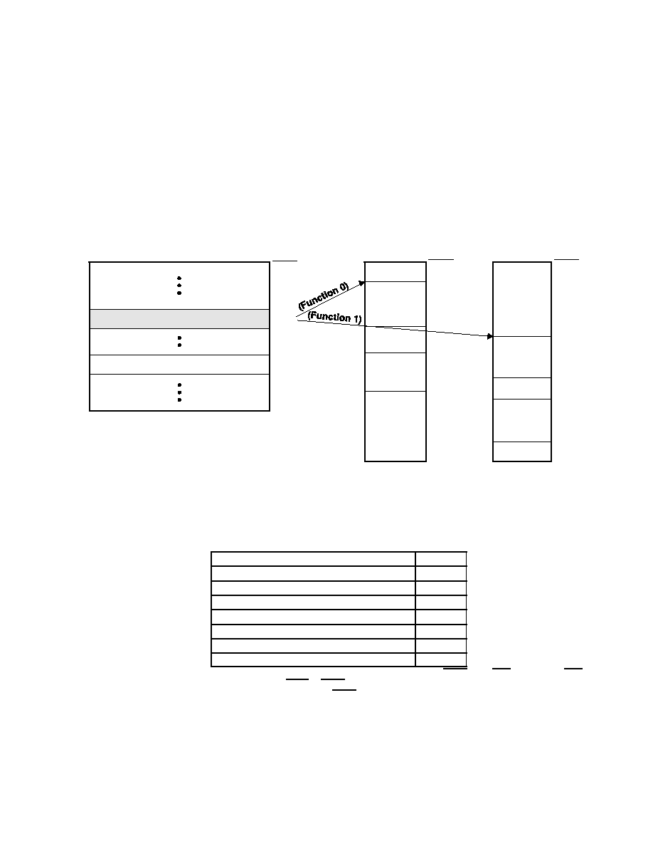
6≠1
6 CardBus Socket Registers (Functions 0 and 1)
The 1997 PC Card Standard requires a CardBus socket controller to provide five 32-bit registers that report and
control socket-specific functions. The PCI7x20 device provides the CardBus socket/ExCA base address register (PCI
offset 10h, see Section 4.12) to locate these CardBus socket registers in PCI memory address space. Each function
has a separate base address register for accessing the CardBus socket registers (see Figure 6≠1). Table 6≠1 gives
the location of the socket registers in relation to the CardBus socket/ExCA base address.
In addition to the five required registers, the PCI7x20 device implements a register at offset 20h that provides power
management control for the socket.
16-Bit Legacy-Mode Base Address
CardBus Socket/ExCA Base Address
10h
44h
CardBus
Socket A
Registers
ExCA
Registers
Card A
20h
800h
844h
Host
Memory Space
CardBus
Socket B
Registers
ExCA
Registers
Card B
20h
800h
844h
Host
Memory Space
Note: The CardBus socket/ExCA base
address mode register is separate for
functions 0 and 1.
address register's base address.
Offsets are from the CardBus socket/ExCA base
00h
00h
PCI7x20 Configuration Registers
Offset
Offset
Offset
Figure 6≠1. Accessing CardBus Socket Registers Through PCI Memory
Table 6≠1. CardBus Socket Registers
REGISTER NAME
OFFSET
Socket event
00h
Socket mask
04h
Socket present state
08h
Socket force event
0Ch
Socket control
10h
Reserved
14h≠1Ch
Socket power management
20h
One or more bits in the register are PME context bits and can be cleared only by the assertion of GRST when PME is enabled. If PME is not
enabled, then these bits are cleared by the assertion of PRST or GRST.
One or more bits in this register are cleared only by the assertion of GRST.

6≠2
6.1
Socket Event Register
This register indicates a change in socket status has occurred. These bits do not indicate what the change is, only
that one has occurred. Software must read the socket present state register for current status. Each bit in this register
can be cleared by writing a 1 to that bit. The bits in this register can be set to a 1 by software through writing a 1 to
the corresponding bit in the socket force event register. All bits in this register are cleared by PCI reset. They can be
immediately set again, if, when coming out of PC Card reset, the bridge finds the status unchanged (i.e., CSTSCHG
reasserted or card detect is still true). Software needs to clear this register before enabling interrupts. If it is not cleared
and interrupts are enabled, then an unmasked interrupt is generated based on any bit that is set. See Table 6≠2 for
a complete description of the register contents.
Bit
31
30
29
28
27
26
25
24
23
22
21
20
19
18
17
16
Name
Socket event
Type
R
R
R
R
R
R
R
R
R
R
R
R
R
R
R
R
Default
0
0
0
0
0
0
0
0
0
0
0
0
0
0
0
0
Bit
15
14
13
12
11
10
9
8
7
6
5
4
3
2
1
0
Name
Socket event
Type
R
R
R
R
R
R
R
R
R
R
R
R
RWC
RWC
RWC
RWC
Default
0
0
0
0
0
0
0
0
0
0
0
0
0
0
0
0
Register:
Socket event
Offset:
CardBus Socket Address + 00h
Type:
Read-only, Read/Write to Clear
Default: 0000 0000h
Table 6≠2. Socket Event Register Description
BIT
SIGNAL
TYPE
FUNCTION
31≠4
RSVD
R
These bits return 0s when read.
3
PWREVENT
RWC
Power cycle. This bit is set when the PCI7x20 device detects that the PWRCYCLE bit in the socket present
state register (offset 08h, see Section 6.3) has changed. This bit is cleared by writing a 1.
2
CD2EVENT
RWC
CCD2. This bit is set when the PCI7x20 device detects that the CDETECT2 field in the socket present state
register (offset 08h, see Section 6.3) has changed. This bit is cleared by writing a 1.
1
CD1EVENT
RWC
CCD1. This bit is set when the PCI7x20 device detects that the CDETECT1 field in the socket present state
register (offset 08h, see Section 6.3) has changed. This bit is cleared by writing a 1.
0
CSTSEVENT
RWC
CSTSCHG. This bit is set when the CARDSTS field in the socket present state register (offset 08h, see
Section 6.3) has changed state. For CardBus cards, this bit is set on the rising edge of the CSTSCHG
signal. For 16-bit PC Cards, this bit is set on both transitions of the CSTSCHG signal. This bit is reset by
writing a 1.
This bit is cleared only by the assertion of GRST when PME is enabled. If PME is not enabled, then this bit is cleared by the assertion of PRST
or GRST.

6≠3
6.2
Socket Mask Register
This register allows software to control the CardBus card events which generate a status change interrupt. The state
of these mask bits does not prevent the corresponding bits from reacting in the socket event register (offset 00h, see
Section 6.1). See Table 6≠3 for a complete description of the register contents.
Bit
31
30
29
28
27
26
25
24
23
22
21
20
19
18
17
16
Name
Socket mask
Type
R
R
R
R
R
R
R
R
R
R
R
R
R
R
R
R
Default
0
0
0
0
0
0
0
0
0
0
0
0
0
0
0
0
Bit
15
14
13
12
11
10
9
8
7
6
5
4
3
2
1
0
Name
Socket mask
Type
R
R
R
R
R
R
R
R
R
R
R
R
RW
RW
RW
RW
Default
0
0
0
0
0
0
0
0
0
0
0
0
0
0
0
0
Register:
Socket mask
Offset:
CardBus Socket Address + 04h
Type:
Read-only, Read/Write
Default: 0000 0000h
Table 6≠3. Socket Mask Register Description
BIT
SIGNAL
TYPE
FUNCTION
31≠4
RSVD
R
These bits return 0s when read.
3
PWRMASK
RW
Power cycle. This bit masks the PWRCYCLE bit in the socket present state register (offset 08h, see
Section 6.3) from causing a status change interrupt.
0 = PWRCYCLE event does not cause a CSC interrupt (default).
1 = PWRCYCLE event causes a CSC interrupt.
2≠1
CDMASK
RW
Card detect mask. These bits mask the CDETECT1 and CDETECT2 bits in the socket present state
register (offset 08h, see Section 6.3) from causing a CSC interrupt.
00 = Insertion/removal does not cause a CSC interrupt (default).
01 = Reserved (undefined)
10 = Reserved (undefined)
11 = Insertion/removal causes a CSC interrupt.
0
CSTSMASK
RW
CSTSCHG mask. This bit masks the CARDSTS field in the socket present state register (offset 08h, see
Section 6.3) from causing a CSC interrupt.
0 = CARDSTS event does not cause a CSC interrupt (default).
1 = CARDSTS event causes a CSC interrupt.
This bit is cleared only by the assertion of GRST when PME is enabled. If PME is not enabled, then this bit is cleared by the assertion of PRST
or GRST.

6≠4
6.3
Socket Present State Register
This register reports information about the socket interface. Writes to the socket force event register (offset 0Ch, see
Section 6.4), as well as general socket interface status, are reflected here. Information about PC Card V
CC
support
and card type is only updated at each insertion. Also note that the PCI7x20 device uses the CCD1 and CCD2 signals
during card identification, and changes on these signals during this operation are not reflected in this register.
Bit
31
30
29
28
27
26
25
24
23
22
21
20
19
18
17
16
Name
Socket present state
Type
R
R
R
R
R
R
R
R
R
R
R
R
R
R
R
R
Default
0
0
1
1
0
0
0
0
0
0
0
0
0
0
0
0
Bit
15
14
13
12
11
10
9
8
7
6
5
4
3
2
1
0
Name
Socket present state
Type
R
R
R
R
R
R
R
R
R
R
R
R
R
R
R
R
Default
0
0
0
0
0
0
0
0
0
X
0
0
0
X
X
X
Register:
Socket present state
Offset:
CardBus Socket Address + 08h
Type:
Read-only
Default: 3000 00XXh
Table 6≠4. Socket Present State Register Description
BIT
SIGNAL
TYPE
FUNCTION
31
YVSOCKET
R
YV socket. This bit indicates whether or not the socket can supply VCC = Y.Y V to PC Cards. The
PCI7x20 device does not support Y.Y-V VCC; therefore, this bit is always reset unless overridden by
the socket force event register (offset 0Ch, see Section 6.4). This bit defaults to 0.
30
XVSOCKET
R
XV socket. This bit indicates whether or not the socket can supply VCC = X.X V to PC Cards. The
PCI7x20 device does not support X.X-V VCC; therefore, this bit is always reset unless overridden by
the socket force event register (offset 0Ch, see Section 6.4). This bit defaults to 0.
29
3VSOCKET
R
3-V socket. This bit indicates whether or not the socket can supply VCC = 3.3 Vdc to PC Cards. The
PCI7x20 device does support 3.3-V VCC; therefore, this bit is always set unless overridden by the
socket force event register (offset 0Ch, see Section 6.4).
28
5VSOCKET
R
5-V socket. This bit indicates whether or not the socket can supply VCC = 5 Vdc to PC Cards. The
PCI7x20 device does support 5-V VCC; therefore, this bit is always set unless overridden by bit 6 of
the device control register (PCI offset 92h, see Section 4.39).
27≠14
RSVD
R
These bits return 0s when read.
13
YVCARD
R
YV card. This bit indicates whether or not the PC Card inserted in the socket supports VCC = Y.Y Vdc.
This bit can be set by writing a 1 to the corresponding bit in the socket force event register (offset 0Ch,
see Section 6.4).
12
XVCARD
R
XV card. This bit indicates whether or not the PC Card inserted in the socket supports VCC = X.X Vdc.
This bit can be set by writing a 1 to the corresponding bit in the socket force event register (offset 0Ch,
see Section 6.4).
11
3VCARD
R
3-V card. This bit indicates whether or not the PC Card inserted in the socket supports VCC = 3.3 Vdc.
This bit can be set by writing a 1 to the corresponding bit in the socket force event register (offset 0Ch,
see Section 6.4).
10
5VCARD
R
5-V card. This bit indicates whether or not the PC Card inserted in the socket supports VCC = 5 Vdc.
This bit can be set by writing a 1 to the corresponding bit in the socket force event register (offset 0Ch,
see Section 6.4).
One or more bits in the register are PME context bits and can be cleared only by the assertion of GRST when PME is enabled. If PME is not
enabled, then these bits are cleared by the assertion of PRST or GRST.

6≠5
Table 6≠4.
Socket Present State Register Description (Continued)
BIT
SIGNAL
TYPE
FUNCTION
9
BADVCCREQ
R
Bad VCC request. This bit indicates that the host software has requested that the socket be powered at
an invalid voltage.
0 = Normal operation (default)
1 = Invalid VCC request by host software
8
DATALOST
R
Data lost. This bit indicates that a PC Card removal event may have caused lost data because the cycle
did not terminate properly or because write data still resides in the PCI7x20 device.
0 = Normal operation (default)
1 = Potential data loss due to card removal
7
NOTACARD
R
Not a card. This bit indicates that an unrecognizable PC Card has been inserted in the socket. This bit is
not updated until a valid PC Card is inserted into the socket.
0 = Normal operation (default)
1 = Unrecognizable PC Card detected
6
IREQCINT
R
READY(IREQ)//CINT. This bit indicates the current status of the READY(IREQ)//CINT signal at the PC
Card interface.
0 = READY(IREQ)//CINT is low.
1 = READY(IREQ)//CINT is high.
5
CBCARD
R
CardBus card detected. This bit indicates that a CardBus PC Card is inserted in the socket. This bit is not
updated until another card interrogation sequence occurs (card insertion).
4
16BITCARD
R
16-bit card detected. This bit indicates that a 16-bit PC Card is inserted in the socket. This bit is not
updated until another card interrogation sequence occurs (card insertion).
3
PWRCYCLE
R
Power cycle. This bit indicates the status of each card powering request. This bit is encoded as:
0 = Socket is powered down (default).
1 = Socket is powered up.
2
CDETECT2
R
CCD2. This bit reflects the current status of the CCD2 signal at the PC Card interface. Changes to this
signal during card interrogation are not reflected here.
0 = CCD2 is low (PC Card may be present)
1 = CCD2 is high (PC Card not present)
1
CDETECT1
R
CCD1. This bit reflects the current status of the CCD1 signal at the PC Card interface. Changes to this
signal during card interrogation are not reflected here.
0 = CCD1 is low (PC Card may be present).
1 = CCD1 is high (PC Card not present).
0
CARDSTS
R
CSTSCHG. This bit reflects the current status of the CSTSCHG signal at the PC Card interface.
0 = CSTSCHG is low.
1 = CSTSCHG is high.
One or more bits in the register are PME context bits and can be cleared only by the assertion of GRST when PME is enabled. If PME is not
enabled, then these bits are cleared by the assertion of PRST or GRST.
6.4
Socket Force Event Register
This register is used to force changes to the socket event register (offset 00h, see Section 6.1) and the socket present
state register (offset 08h, see Section 6.3). The CVSTEST bit (bit 14) in this register must be written when forcing
changes that require card interrogation. See Table 6≠5 for a complete description of the register contents.
Bit
31
30
29
28
27
26
25
24
23
22
21
20
19
18
17
16
Name
Socket force event
Type
R
R
R
R
R
R
R
R
R
R
R
R
R
R
R
R
Default
0
0
0
0
0
0
0
0
0
0
0
0
0
0
0
0
Bit
15
14
13
12
11
10
9
8
7
6
5
4
3
2
1
0
Name
Socket force event
Type
R
W
W
W
W
W
W
W
W
R
W
W
W
W
W
W
Default
X
X
X
X
X
X
X
X
X
X
X
X
X
X
X
X
Register:
Socket force event
Offset:
CardBus Socket Address + 0Ch
Type:
Read-only, Write-only
Default: 0000 XXXXh

6≠6
Table 6≠5. Socket Force Event Register Description
BIT
SIGNAL
TYPE
FUNCTION
31≠15
RSVD
R
Reserved. These bits return 0s when read.
14
CVSTEST
W
Card VS test. When this bit is set, the PCI7x20 device reinterrogates the PC Card, updates the socket
present state register (offset 08h, see Section 6.3), and re-enables the socket power control.
13
FYVCARD
W
Force YV card. Writes to this bit cause the YVCARD bit in the socket present state register (offset 08h,
see Section 6.3) to be written. When set, this bit disables the socket power control.
12
FXVCARD
W
Force XV card. Writes to this bit cause the XVCARD bit in the socket present state register (offset 08h,
see Section 6.3) to be written. When set, this bit disables the socket power control.
11
F3VCARD
W
Force 3-V card. Writes to this bit cause the 3VCARD bit in the socket present state register (offset 08h,
see Section 6.3) to be written. When set, this bit disables the socket power control.
10
F5VCARD
W
Force 5-V card. Writes to this bit cause the 5VCARD bit in the socket present state register (offset 08h,
see Section 6.3) to be written. When set, this bit disables the socket power control.
9
FBADVCCREQ
W
Force BadVccReq. Changes to the BADVCCREQ bit in the socket present state register (offset 08h,
see Section 6.3) can be made by writing this bit.
8
FDATALOST
W
Force data lost. Writes to this bit cause the DATALOST bit in the socket present state register (offset
08h, see Section 6.3) to be written.
7
FNOTACARD
W
Force not a card. Writes to this bit cause the NOTACARD bit in the socket present state register (offset
08h, see Section 6.3) to be written.
6
RSVD
R
This bit returns 0 when read.
5
FCBCARD
W
Force CardBus card. Writes to this bit cause the CBCARD bit in the socket present state register (offset
08h, see Section 6.3) to be written.
4
F16BITCARD
W
Force 16-bit card. Writes to this bit cause the 16BITCARD bit in the socket present state register (offset
08h, see Section 6.3) to be written.
3
FPWRCYCLE
W
Force power cycle. Writes to this bit cause the PWREVENT bit in the socket event register (offset 00h,
see Section 6.1) to be written, and the PWRCYCLE bit in the socket present state register (offset 08h,
see Section 6.3) is unaffected.
2
FCDETECT2
W
Force CCD2. Writes to this bit cause the CD2EVENT bit in the socket event register (offset 00h, see
Section 6.1) to be written, and the CDETECT2 bit in the socket present state register (offset 08h, see
Section 6.3) is unaffected.
1
FCDETECT1
W
Force CCD1. Writes to this bit cause the CD1EVENT bit in the socket event register (offset 00h, see
Section 6.1) to be written, and the CDETECT1 bit in the socket present state register (offset 08h, see
Section 6.3) is unaffected.
0
FCARDSTS
W
Force CSTSCHG. Writes to this bit cause the CSTSEVENT bit in the socket event register (offset 00h,
see Section 6.1) to be written. The CARDSTS bit in the socket present state register (offset 08h, see
Section 6.3) is unaffected.
6≠7
6.5
Socket Control Register
This register provides control of the voltages applied to the socket V
PP
and V
CC
. The PCI7x20 device ensures that
the socket is powered up only at acceptable voltages when a CardBus card is inserted. See Table 6≠6 for a complete
description of the register contents.
Bit
31
30
29
28
27
26
25
24
23
22
21
20
19
18
17
16
Name
Socket control
Type
R
R
R
R
R
R
R
R
R
R
R
R
R
R
R
R
Default
0
0
0
0
0
0
0
0
0
0
0
0
0
0
0
0
Bit
15
14
13
12
11
10
9
8
7
6
5
4
3
2
1
0
Name
Socket control
Type
R
R
R
R
R
R
RW
R
RW
RW
RW
RW
R
RW
RW
RW
Default
0
0
0
0
0
0
0
0
0
0
0
0
0
0
0
0
Register:
Socket control
Offset:
CardBus Socket Address + 10h
Type:
Read-only, Read/Write
Default: 0000 0000h
Table 6≠6. Socket Control Register Description
BIT
SIGNAL
TYPE
FUNCTION
31≠11
RSVD
R
These bits return 0s when read.
10
RSVD
R
This bit returns 1 when read.
9≠8
RSVD
R
These bits return 0s when read.
7
STOPCLK
RW
This bit controls how the CardBus clock run state machine decides when to stop the CardBus clock
to the CardBus card:
0 = The CardBus CLKRUN protocol can only attempt to stop/slow the CaredBus clock if the
sockethas been idle for 8 clocks and the PCI CLKRUN protocol is preparing to stop/slow the
PCI bus clock.
1 = The CardBus CLKRUN protocol can only attempt to stop/slow the CaredBus clock if the
socket has been idle for 8 clocks, regardless of the state of the PCI CLKRUN signal.
6≠4
VCCCTRL
RW
VCC control. These bits are used to request card VCC changes.
000 = Request power off (default)
100 = Request VCC = X.X V
001 = Reserved
101 = Request VCC = Y.Y V
010 = Request VCC = 5 V
110 = Reserved
011 = Request VCC = 3.3 V
111 = Reserved
3
RSVD
R
This bit returns 0 when read.
2≠0
VPPCTRL
RW
VPP control. These bits are used to request card VPP changes.
000 = Request power off (default)
100 = Request VPP = X.X V
001 = Request VPP = 12 V
101 = Request VPP = Y.Y V
010 = Request VPP = 5 V
110 = Reserved
011 = Request VPP = 3.3 V
111 = Reserved
One or more bits in the register are PME context bits and can be cleared only by the assertion of GRST when PME is enabled. If PME is not
enabled, then this bit is cleared by the assertion of PRST or GRST.

6≠8
6.6
Socket Power Management Register
This register provides power management control over the socket through a mechanism for slowing or stopping the
clock on the card interface when the card is idle. See Table 6≠7 for a complete description of the register contents.
Bit
31
30
29
28
27
26
25
24
23
22
21
20
19
18
17
16
Name
Socket power management
Type
R
R
R
R
R
R
R
R
R
R
R
R
R
R
R
RW
Default
0
0
0
0
0
0
0
0
0
0
0
0
0
0
0
0
Bit
15
14
13
12
11
10
9
8
7
6
5
4
3
2
1
0
Name
Socket power management
Type
R
R
R
R
R
R
R
R
R
R
R
R
R
R
R
RW
Default
0
0
0
0
0
0
0
0
0
0
0
0
0
0
0
0
Register:
Socket power management
Offset:
CardBus Socket Address + 20h
Type:
Read-only, Read/Write
Default: 0000 0000h
Table 6≠7. Socket Power Management Register Description
BIT
SIGNAL
TYPE
FUNCTION
31≠26
RSVD
R
Reserved. These bits return 0s when read.
25
SKTACCES
R
Socket access status. This bit provides information on whether a socket access has occurred. This bit is
cleared by a read access.
0 = No PC Card access has occurred (default).
1 = PC Card has been accessed.
24
SKTMODE
R
Socket mode status. This bit provides clock mode information.
0 = Normal clock operation
1 = Clock frequency has changed.
23≠17
RSVD
R
These bits return 0s when read.
16
CLKCTRLEN
RW
CardBus clock control enable. This bit, when set, enables clock control according to bit 0 (CLKCTRL).
0 = Clock control disabled (default)
1 = Clock control enabled
15≠1
RSVD
R
These bits return 0s when read.
0
CLKCTRL
RW
CardBus clock control. This bit determines whether the CardBus CLKRUN protocol attempts to stop or
slow the CardBus clock during idle states. The CLKCTRLEN bit enables this bit.
0 = Allows the CardBus CLKRUN protocol to attempt to stop the CardBus clock (default)
1 = Allows the CardBus CLKRUN protocol to attempt to slow the CardBus clock by a factor of 16
One or more bits in this register are cleared only by the assertion of GRST.

7≠1
7 OHCI Controller Programming Model
This section describes the internal PCI configuration registers used to program the PCI7x20 1394 open host controller
interface. All registers are detailed in the same format: a brief description for each register is followed by the register
offset and a bit table describing the reset state for each register.
A bit description table, typically included when the register contains bits of more than one type or purpose, indicates
bit field names, a detailed field description, and field access tags which appear in the type column. Table 4≠1
describes the field access tags.
PCI7x20 device is a multifunction PCI device. The 1394 OHCI is integrated as PCI function 2. The function 2
configuration header is compliant with the PCI Local Bus Specification as a standard header. Table 7≠1 illustrates
the configuration header that includes both the predefined portion of the configuration space and the user-definable
registers.
Table 7≠1. Function 2 Configuration Register Map
REGISTER NAME
OFFSET
Device ID
Vendor ID
00h
Status
Command
04h
Class code
Revision ID
08h
BIST
Header type
Latency timer
Cache line size
0Ch
OHCI base address
10h
TI extension base address
14h
CardBus CIS base address
18h
Reserved
1Ch≠27h
CardBus CIS pointer
28h
Subsystem ID
Subsystem vendor ID
2Ch
Reserved
30h
Reserved
PCI power
management
capabilities pointer
34h
Reserved
38h
Maximum latency
Minimum grant
Interrupt pin
Interrupt line
3Ch
PCI OHCI control
40h
Power management capabilities
Next item pointer
Capability ID
44h
PM data
PMCSR_BSE
Power management control and status
48h
Reserved
4Ch≠ECh
PCI miscellaneous configuration
F0h
Link enhancement control
F4h
Subsystem access
F8h
GPIO control
FCh
One or more bits in this register are cleared only by the assertion of GRST.

7≠2
7.1
Vendor ID Register
The vendor ID register contains a value allocated by the PCI SIG and identifies the manufacturer of the PCI device.
The vendor ID assigned to Texas Instruments is 104Ch.
Bit
15
14
13
12
11
10
9
8
7
6
5
4
3
2
1
0
Name
Vendor ID
Type
R
R
R
R
R
R
R
R
R
R
R
R
R
R
R
R
Default
0
0
0
1
0
0
0
0
0
1
0
0
1
1
0
0
Register:
Vendor ID
Offset:
00h
Type:
Read-only
Default:
104Ch
7.2
Device ID Register
The device ID register contains a value assigned to the PCI7x20 device by Texas Instruments. The device
identification for the PCI7x20 device is 802Eh.
Bit
15
14
13
12
11
10
9
8
7
6
5
4
3
2
1
0
Name
Device ID
Type
R
R
R
R
R
R
R
R
R
R
R
R
R
R
R
R
Default
1
0
0
0
0
0
0
0
0
0
1
0
1
1
1
0
Register:
Device ID
Offset:
02h
Type:
Read-only
Default:
802Eh

7≠3
7.3
Command Register
The command register provides control over the PCI7x20 interface to the PCI bus. All bit functions adhere to the
definitions in the PCI Local Bus Specification, as seen in the following bit descriptions. See Table 7≠2 for a complete
description of the register contents.
Bit
15
14
13
12
11
10
9
8
7
6
5
4
3
2
1
0
Name
Command
Type
R
R
R
R
R
RW
R
RW
R
RW
R
RW
R
RW
RW
R
Default
0
0
0
0
0
0
0
0
0
0
0
0
0
0
0
0
Register:
Command
Offset:
04h
Type:
Read/Write, Read-only
Default:
0000h
Table 7≠2. Command Register Description
BIT
FIELD NAME
TYPE
DESCRIPTION
15≠11
RSVD
R
Reserved. Bits 15≠11 return 0s when read.
10
INT_DISABLE
RW
INTx disable. When set to 1, this bit disables the function from asserting interrupts on the INTx signals.
0 = INTx assertion is enabled (default)
1 = INTx assertion is disabled
9
FBB_ENB
R
Fast back-to-back enable. The PCI7x20 device does not generate fast back-to-back transactions;
therefore, bit 9 returns 0 when read.
8
SERR_ENB
RW
SERR enable. When bit 8 is set to 1, the PCI7x20 SERR driver is enabled. SERR can be asserted after
detecting an address parity error on the PCI bus.
7
RSVD
R
Reserved. Bit 7 returns 0 when read.
6
PERR_ENB
RW
Parity error enable. When bit 6 is set to 1, the PCI7x20 device is enabled to drive PERR response to
parity errors through the PERR signal.
5
VGA_ENB
R
VGA palette snoop enable. The PCI7x20 device does not feature VGA palette snooping; therefore, bit
5 returns 0 when read.
4
MWI_ENB
RW
Memory write and invalidate enable. When bit 4 is set to 1, the PCI7x20 device is enabled to generate
MWI PCI bus commands. If this bit is cleared, then the PCI7x20 device generates memory write
commands instead.
3
SPECIAL
R
Special cycle enable. The PCI7x20 function does not respond to special cycle transactions; therefore,
bit 3 returns 0 when read.
2
MASTER_ENB
RW
Bus master enable. When bit 2 is set to 1, the PCI7x20 device is enabled to initiate cycles on the PCI
bus.
1
MEMORY_ENB
RW
Memory response enable. Setting bit 1 to 1 enables the PCI7x20 device to respond to memory cycles
on the PCI bus. This bit must be set to access OHCI registers.
0
IO_ENB
R
I/O space enable. The PCI7x20 device does not implement any I/O-mapped functionality; therefore,
bit 0 returns 0 when read.

7≠4
7.4
Status Register
The status register provides status over the PCI7x20 interface to the PCI bus. All bit functions adhere to the definitions
in the PCI Local Bus Specification, as seen in the following bit descriptions. See Table 7≠3 for a complete description
of the register contents.
Bit
15
14
13
12
11
10
9
8
7
6
5
4
3
2
1
0
Name
Status
Type
RCU
RCU
RCU
RCU
RCU
R
R
RCU
R
R
R
R
RU
R
R
R
Default
0
0
0
0
0
0
1
0
0
0
0
1
0
0
0
0
Register:
Status
Offset:
06h
Type:
Read/Clear/Update, Read-only
Default:
0210h
Table 7≠3. Status Register Description
BIT
FIELD NAME
TYPE
DESCRIPTION
15
PAR_ERR
RCU
Detected parity error. Bit 15 is set to 1 when either an address parity or data parity error is detected.
14
SYS_ERR
RCU
Signaled system error. Bit 14 is set to 1 when SERR is enabled and the PCI7x20 device has signaled
a system error to the host.
13
MABORT
RCU
Received master abort. Bit 13 is set to 1 when a cycle initiated by the PCI7x20 device on the PCI bus
has been terminated by a master abort.
12
TABORT_REC
RCU
Received target abort. Bit 12 is set to 1 when a cycle initiated by the PCI7x20 device on the PCI bus
was terminated by a target abort.
11
TABORT_SIG
RCU
Signaled target abort. Bit 11 is set to 1 by the PCI7x20 device when it terminates a transaction on the
PCI bus with a target abort.
10≠9
PCI_SPEED
R
DEVSEL timing. Bits 10 and 9 encode the timing of DEVSEL and are hardwired to 01b, indicating that
the PCI7x20 device asserts this signal at a medium speed on nonconfiguration cycle accesses.
8
DATAPAR
RCU
Data parity error detected. Bit 8 is set to 1 when the following conditions have been met:
a. PERR was asserted by any PCI device including the PCI7x20 device.
b. The PCI7x20 device was the bus master during the data parity error.
c. Bit 6 (PERR_EN) in the command register at offset 04h in the PCI configuration space
(see Section 7.3) is set to 1.
7
FBB_CAP
R
Fast back-to-back capable. The PCI7x20 device cannot accept fast back-to-back transactions;
therefore, bit 7 is hardwired to 0.
6
UDF
R
User-definable features (UDF) supported. The PCI7x20 device does not support the UDF; therefore,
bit 6 is hardwired to 0.
5
66MHZ
R
66-MHz capable. The PCI7x20 device operates at a maximum PCLK frequency of 33 MHz; therefore,
bit 5 is hardwired to 0.
4
CAPLIST
R
Capabilities list. Bit 4 returns 1 when read, indicating that capabilities additional to standard PCI are
implemented. The linked list of PCI power-management capabilities is implemented in this function.
3
INT_STATUS
RU
Interrupt status. This bit reflects the interrupt status of the function. Only when bit 10 (INT_DISABLE)
in the command register (see Section 7.3) is a 0 and this bit is 1, is the function's INTx signal asserted.
Setting the INT_DISABLE bit to 1 has no effect on the state of this bit.
2≠0
RSVD
R
Reserved. Bits 3≠0 return 0s when read.

7≠5
7.5
Class Code and Revision ID Register
The class code and revision ID register categorizes the PCI7x20 device as a serial bus controller (0Ch), controlling
an IEEE 1394 bus (00h), with an OHCI programming model (10h). Furthermore, the TI chip revision is indicated in
the least significant byte. See Table 7≠4 for a complete description of the register contents.
Bit
31
30
29
28
27
26
25
24
23
22
21
20
19
18
17
16
Name
Class code and revision ID
Type
R
R
R
R
R
R
R
R
R
R
R
R
R
R
R
R
Default
0
0
0
0
1
1
0
0
0
0
0
0
0
0
0
0
Bit
15
14
13
12
11
10
9
8
7
6
5
4
3
2
1
0
Name
Class code and revision ID
Type
R
R
R
R
R
R
R
R
R
R
R
R
R
R
R
R
Default
0
0
0
1
0
0
0
0
0
0
0
0
0
0
0
0
Register:
Class code and revision ID
Offset:
08h
Type:
Read-only
Default:
0C00 1000h
Table 7≠4. Class Code and Revision ID Register Description
BIT
FIELD NAME
TYPE
DESCRIPTION
31≠24
BASECLASS
R
Base class. This field returns 0Ch when read, which broadly classifies the function as a serial bus
controller.
23≠16
SUBCLASS
R
Subclass. This field returns 00h when read, which specifically classifies the function as controlling an
IEEE 1394 serial bus.
15≠8
PGMIF
R
Programming interface. This field returns 10h when read, which indicates that the programming model
is compliant with the 1394 Open Host Controller Interface Specification.
7≠0
CHIPREV
R
Silicon revision. This field returns 00h when read, which indicates the silicon revision of the PCI7x20
device.
7.6
Latency Timer and Class Cache Line Size Register
The latency timer and class cache line size register is programmed by host BIOS to indicate system cache line size
and the latency timer associated with the PCI7x20 device. See Table 7≠5 for a complete description of the register
contents.
Bit
15
14
13
12
11
10
9
8
7
6
5
4
3
2
1
0
Name
Latency timer and class cache line size
Type
RW
RW
RW
RW
RW
RW
RW
RW
RW
RW
RW
RW
RW
RW
RW
RW
Default
0
0
0
0
0
0
0
0
0
0
0
0
0
0
0
0
Register:
Latency timer and class cache line size
Offset:
0Ch
Type:
Read/Write
Default:
0000h
Table 7≠5. Latency Timer and Class Cache Line Size Register Description
BIT
FIELD NAME
TYPE
DESCRIPTION
15≠8
LATENCY_TIMER
RW
PCI latency timer. The value in this register specifies the latency timer for the PCI7x20 device, in units
of PCI clock cycles. When the PCI7x20 device is a PCI bus initiator and asserts FRAME, the latency
timer begins counting from zero. If the latency timer expires before the PCI7x20 transaction has
terminated, then the PCI7x20 device terminates the transaction when its GNT is deasserted.
7≠0
CACHELINE_SZ
RW
Cache line size. This value is used by the PCI7x20 device during memory write and invalidate,
memory-read line, and memory-read multiple transactions.

7≠6
7.7
Header Type and BIST Register
The header type and built-in self-test (BIST) register indicates the PCI7x20 PCI header type and no built-in self-test.
See Table 7≠6 for a complete description of the register contents.
Bit
15
14
13
12
11
10
9
8
7
6
5
4
3
2
1
0
Name
Header type and BIST
Type
R
R
R
R
R
R
R
R
R
R
R
R
R
R
R
R
Default
0
0
0
0
0
0
0
0
0
0
0
0
0
0
0
0
Register:
Header type and BIST
Offset:
0Eh
Type:
Read-only
Default:
0000h
Table 7≠6. Header Type and BIST Register Description
BIT
FIELD NAME
TYPE
DESCRIPTION
15≠8
BIST
R
Built-in self-test. The PCI7x20 device does not include a BIST; therefore, this field returns 00h when
read.
7≠0
HEADER_TYPE
R
PCI header type. The PCI7x20 device includes the standard PCI header, which is communicated by
returning 00h when this field is read.
7.8
OHCI Base Address Register
The OHCI base address register is programmed with a base address referencing the memory-mapped OHCI control.
When BIOS writes all 1s to this register, the value read back is FFFF F800h, indicating that at least 2K bytes of
memory address space are required for the OHCI registers. See Table 7≠7 for a complete description of the register
contents.
Bit
31
30
29
28
27
26
25
24
23
22
21
20
19
18
17
16
Name
OHCI base address
Type
RW
RW
RW
RW
RW
RW
RW
RW
RW
RW
RW
RW
RW
RW
RW
RW
Default
0
0
0
0
0
0
0
0
0
0
0
0
0
0
0
0
Bit
15
14
13
12
11
10
9
8
7
6
5
4
3
2
1
0
Name
OHCI base address
Type
RW
RW
RW
RW
RW
R
R
R
R
R
R
R
R
R
R
R
Default
0
0
0
0
0
0
0
0
0
0
0
0
0
0
0
0
Register:
OHCI base address
Offset:
10h
Type:
Read/Write, Read-only
Default:
0000 0000h
Table 7≠7. OHCI Base Address Register Description
BIT
FIELD NAME
TYPE
DESCRIPTION
31≠11
OHCIREG_PTR
RW
OHCI register pointer. This field specifies the upper 21 bits of the 32-bit OHCI base address register.
10≠4
OHCI_SZ
R
OHCI register size. This field returns 0s when read, indicating that the OHCI registers require a
2K-byte region of memory.
3
OHCI_PF
R
OHCI register prefetch. Bit 3 returns 0 when read, indicating that the OHCI registers are
nonprefetchable.
2≠1
OHCI_MEMTYPE
R
OHCI memory type. This field returns 0s when read, indicating that the OHCI base address register
is 32 bits wide and mapping can be done anywhere in the 32-bit memory space.
0
OHCI_MEM
R
OHCI memory indicator. Bit 0 returns 0 when read, indicating that the OHCI registers are mapped
into system memory space.

7≠7
7.9
TI Extension Base Address Register
The TI extension base address register is programmed with a base address referencing the memory-mapped TI
extension registers. When BIOS writes all 1s to this register, the value read back is FFFF C000h, indicating that at
least 16K bytes of memory address space are required for the TI registers. See Table 7≠8 for a complete description
of the register contents.
Bit
31
30
29
28
27
26
25
24
23
22
21
20
19
18
17
16
Name
TI extension base address
Type
RW
RW
RW
RW
RW
RW
RW
RW
RW
RW
RW
RW
RW
RW
RW
RW
Default
0
0
0
0
0
0
0
0
0
0
0
0
0
0
0
0
Bit
15
14
13
12
11
10
9
8
7
6
5
4
3
2
1
0
Name
TI extension base address
Type
RW
RW
R
R
R
R
R
R
R
R
R
R
R
R
R
R
Default
0
0
0
0
0
0
0
0
0
0
0
0
0
0
0
0
Register:
TI extension base address
Offset:
14h
Type:
Read/Write, Read-only
Default:
0000 0000h
Table 7≠8. TI Base Address Register Description
BIT
FIELD NAME
TYPE
DESCRIPTION
31≠14
TIREG_PTR
RW
TI register pointer. This field specifies the upper 18 bits of the 32-bit TI base address register.
13≠4
TI_SZ
R
TI register size. This field returns 0s when read, indicating that the TI registers require a 16K-byte
region of memory.
3
TI_PF
R
TI register prefetch. Bit 3 returns 0 when read, indicating that the TI registers are nonprefetchable.
2≠1
TI_MEMTYPE
R
TI memory type. This field returns 0s when read, indicating that the TI base address register is 32 bits
wide and mapping can be done anywhere in the 32-bit memory space.
0
TI_MEM
R
TI memory indicator. Bit 0 returns 0 when read, indicating that the TI registers are mapped into system
memory space.

7≠8
7.10 CardBus CIS Base Address Register
The internal CARDBUS input to the 1394 OHCI core is tied high such that this register returns 0s when read. See
Table 7≠9 for a complete description of the register contents.
Bit
31
30
29
28
27
26
25
24
23
22
21
20
19
18
17
16
Name
CardBus CIS base address
Type
RW
RW
RW
RW
RW
RW
RW
RW
RW
RW
RW
RW
RW
RW
RW
RW
Default
0
0
0
0
0
0
0
0
0
0
0
0
0
0
0
0
Bit
15
14
13
12
11
10
9
8
7
6
5
4
3
2
1
0
Name
CardBus CIS base address
Type
RW
RW
RW
RW
RW
R
R
R
R
R
R
R
R
R
R
R
Default
0
0
0
0
0
0
0
0
0
0
0
0
0
0
0
0
Register:
CardBus CIS base address
Offset:
18h
Type:
Read/Write, Read-only
Default:
0000 0000h
Table 7≠9. CardBus CIS Base Address Register Description
BIT
FIELD NAME
TYPE
DESCRIPTION
31≠11
CIS_BASE
RW
CIS base address. This field specifies the upper 21 bits of the 32-bit CIS base address. If CARDBUS
is sampled high on a GRST, then this field is read-only, returning 0s when read.
10≠4
CIS_SZ
R
CIS address space size. This field returns 0s when read, indicating that the CIS space requires a
2K-byte region of memory.
3
CIS_PF
R
CIS prefetch. Bit 3 returns 0 when read, indicating that the CIS is nonprefetchable. Furthermore, the
CIS is a byte-accessible address space, and either a doubleword or 16-bit word access yields
indeterminate results.
2≠1
CIS_MEMTYPE
R
CIS memory type. This field returns 0s when read, indicating that the CardBus CIS base address
register is 32 bits wide and mapping can be done anywhere in the 32-bit memory space.
0
CIS_MEM
R
CIS memory indicator. Bit 0 returns 0 when read, indicating that the CIS is mapped into system
memory space.
7.11 CardBus CIS Pointer Register
The internal CARDBUS input to the 1394 OHCI core is tied high such that this register returns 0s when read.
Bit
31
30
29
28
27
26
25
24
23
22
21
20
19
18
17
16
Name
CardBus CIS pointer
Type
R
R
R
R
R
R
R
R
R
R
R
R
R
R
R
R
Default
0
0
0
0
0
0
0
0
0
0
0
0
0
0
0
0
Bit
15
14
13
12
11
10
9
8
7
6
5
4
3
2
1
0
Name
CardBus CIS pointer
Type
R
R
R
R
R
R
R
R
R
R
R
R
R
R
R
R
Default
0
0
0
0
0
0
0
0
0
0
0
0
0
0
0
0
Register:
CardBus CIS pointer
Offset:
28h
Type:
Read-only
Default:
0000 0000h

7≠9
7.12 Subsystem Identification Register
The subsystem identification register is used for system and option card identification purposes. This register can
be initialized from the serial EEPROM or programmed via the subsystem access register at offset F8h in the PCI
configuration space (see Section 7.24). See Table 7≠10 for a complete description of the register contents.
Bit
31
30
29
28
27
26
25
24
23
22
21
20
19
18
17
16
Name
Subsystem identification
Type
RU
RU
RU
RU
RU
RU
RU
RU
RU
RU
RU
RU
RU
RU
RU
RU
Default
0
0
0
0
0
0
0
0
0
0
0
0
0
0
0
0
Bit
15
14
13
12
11
10
9
8
7
6
5
4
3
2
1
0
Name
Subsystem identification
Type
RU
RU
RU
RU
RU
RU
RU
RU
RU
RU
RU
RU
RU
RU
RU
RU
Default
0
0
0
0
0
0
0
0
0
0
0
0
0
0
0
0
Register:
Subsystem identification
Offset:
2Ch
Type:
Read/Update
Default:
0000 0000h
Table 7≠10. Subsystem Identification Register Description
BIT
FIELD NAME
TYPE
DESCRIPTION
31≠16
OHCI_SSID
RU
Subsystem device ID. This field indicates the subsystem device ID.
15≠0
OHCI_SSVID
RU
Subsystem vendor ID. This field indicates the subsystem vendor ID.
One or more bits in this register are cleared only by the assertion of GRST.
7.13 Power Management Capabilities Pointer Register
The power management capabilities pointer register provides a pointer into the PCI configuration header where the
power-management register block resides. The PCI7x20 configuration header doublewords at offsets 44h and 48h
provide the power-management registers. This register is read-only and returns 44h when read.
Bit
7
6
5
4
3
2
1
0
Name
Power management capabilities pointer
Type
R
R
R
R
R
R
R
R
Default
0
1
0
0
0
1
0
0
Register:
Power management capabilities pointer
Offset:
34h
Type:
Read-only
Default:
44h

7≠10
7.14 Interrupt Line Register
The interrupt line register communicates interrupt line routing information. See Table 7≠11 for a complete description
of the register contents.
Bit
7
6
5
4
3
2
1
0
Name
Interrupt line
Type
RW
RW
RW
RW
RW
RW
RW
RW
Default
0
0
0
0
0
0
0
0
Register:
Interrupt line
Offset:
3Ch
Type:
Read/Write
Default:
00h
Table 7≠11. Interrupt Line Register Description
BIT
FIELD NAME
TYPE
DESCRIPTION
7≠0
INTR_LINE
RW
Interrupt line. This field is programmed by the system and indicates to software which interrupt line the
PCI7x20 PCI_INTA is connected to.
7.15 Interrupt Pin Register
The value read from this register is function dependent and depends on the values of bits 28, the tie-all bit (TIEALL),
and 29, the interrupt tie bit (INTRTIE), in the system control register (PCI offset 80h, see Section 4.29). The INTRTIE
bit is compatible with previous TI CardBus controllers, and when set to 1, ties INTB to INTA internally. The TIEALL
bit ties INTA, INTB, INTC, and INTD together internally. The internal interrupt connections set by INTRTIE and TIEALL
are communicated to host software through this standard register interface. This read-only register is described for
all PCI7x20 functions in Table 7≠12.
Bit
7
6
5
4
3
2
1
0
Name
Interrupt pin
Type
R
R
R
R
R
R
R
R
Default
0
0
0
0
0
0
1
0
Register:
Interrupt pin
Offset:
3Dh
Type:
Read-only
Default: 02h
Table 7≠12. PCI Interrupt Pin Register--Read-Only INTPIN Per Function
INTRTIE BIT
(BIT 29, OFFSET 80h)
TIEALL BIT
(BIT 28, OFFSET 80h)
INTPIN
FUNCTION 0
(CARDBUS)
INTPIN
FUNCTION 1
(DEDICATED SOCKET)
INTPIN
FUNCTION 2
(1394 OHCI)
INTPIN
FUNCTION 3
(FLASH MEDIA)
0
0
01h (INTA)
02h (INTB)
03h (INTC)
Determined by INT_SEL
fi ld i fl
h
di
l
1
0
01h (INTA)
01h (INTA)
03h (INTC)
field in flash media general
control register
X
1
01h (INTA)
01h (INTA)
01h (INTA)
01h (INTA)
NOTE: When configuring the PCI7x20 functions to share PCI interrupts, multifunction terminal MFUNC3 must be configured as IRQSER prior
to setting the INTRTIE bit.

7≠11
7.16 Minimum Grant and Maximum Latency Register
The minimum grant and maximum latency register communicates to the system the desired setting of bits 15≠8 in
the latency timer and class cache line size register at offset 0Ch in the PCI configuration space (see Section 7.6).
If a serial EEPROM is detected, then the contents of this register are loaded through the serial EEPROM interface
after a GRST. If no serial EEPROM is detected, then this register returns a default value that corresponds to the
MAX_LAT = 4, MIN_GNT = 2. See Table 7≠13 for a complete description of the register contents.
Bit
15
14
13
12
11
10
9
8
7
6
5
4
3
2
1
0
Name
Minimum grant and maximum latency
Type
RU
RU
RU
RU
RU
RU
RU
RU
RU
RU
RU
RU
RU
RU
RU
RU
Default
0
0
0
0
0
1
0
0
0
0
0
0
0
0
1
0
Register:
Minimum grant and maximum latency
Offset:
3Eh
Type:
Read/Update
Default:
0402h
Table 7≠13. Minimum Grant and Maximum Latency Register Description
BIT
FIELD NAME
TYPE
DESCRIPTION
15≠8
MAX_LAT
RU
Maximum latency. The contents of this field may be used by host BIOS to assign an arbitration priority level
to the PCI7x20 device. The default for this register indicates that the PCI7x20 device may need to access
the PCI bus as often as every 0.25
µ
s; thus, an extremely high priority level is requested. The contents of
this field may also be loaded through the serial EEPROM.
7≠0
MIN_GNT
RU
Minimum grant. The contents of this field may be used by host BIOS to assign a latency timer register value
to the PCI7x20 device. The default for this register indicates that the PCI7x20 device may need to sustain
burst transfers for nearly 64
µ
s and thus request a large value be programmed in bits 15≠8 of the PCI7x20
latency timer and class cache line size register at offset 0Ch in the PCI configuration space (see
Section 7.6).
One or more bits in this register are cleared only by the assertion of GRST.
7.17 OHCI Control Register
The PCI OHCI control register is defined by the 1394 Open Host Controller Interface Specification and provides a
bit for big endian PCI support. See Table 7≠14 for a complete description of the register contents.
Bit
31
30
29
28
27
26
25
24
23
22
21
20
19
18
17
16
Name
OHCI control
Type
R
R
R
R
R
R
R
R
R
R
R
R
R
R
R
R
Default
0
0
0
0
0
0
0
0
0
0
0
0
0
0
0
0
Bit
15
14
13
12
11
10
9
8
7
6
5
4
3
2
1
0
Name
OHCI control
Type
R
R
R
R
R
R
R
R
R
R
R
R
R
R
R
RW
Default
0
0
0
0
0
0
0
0
0
0
0
0
0
0
0
0
Register:
OHCI control
Offset:
40h
Type:
Read/Write, Read-only
Default:
0000 0000h
Table 7≠14. OHCI Control Register Description
BIT
FIELD NAME
TYPE
DESCRIPTION
31≠1
RSVD
R
Reserved. Bits 31≠1 return 0s when read.
0
GLOBAL_SWAP
RW
When bit 0 is set to 1, all quadlets read from and written to the PCI interface are byte-swapped (big
endian).

7≠12
7.18 Capability ID and Next Item Pointer Registers
The capability ID and next item pointer register identifies the linked-list capability item and provides a pointer to the
next capability item. See Table 7≠15 for a complete description of the register contents.
Bit
15
14
13
12
11
10
9
8
7
6
5
4
3
2
1
0
Name
Capability ID and next item pointer
Type
R
R
R
R
R
R
R
R
R
R
R
R
R
R
R
R
Default
0
0
0
0
0
0
0
0
0
0
0
0
0
0
0
1
Register:
Capability ID and next item pointer
Offset:
44h
Type:
Read-only
Default:
0001h
Table 7≠15. Capability ID and Next Item Pointer Registers Description
BIT
FIELD NAME
TYPE
DESCRIPTION
15≠8
NEXT_ITEM
R
Next item pointer. The PCI7x20 device supports only one additional capability that is communicated
to the system through the extended capabilities list; therefore, this field returns 00h when read.
7≠0
CAPABILITY_ID
R
Capability identification. This field returns 01h when read, which is the unique ID assigned by the PCI
SIG for PCI power-management capability.

7≠13
7.19 Power Management Capabilities Register
The power management capabilities register indicates the capabilities of the PCI7x20 device related to PCI power
management. See Table 7≠16 for a complete description of the register contents.
Bit
15
14
13
12
11
10
9
8
7
6
5
4
3
2
1
0
Name
Power management capabilities
Type
RU
R
R
R
R
R
R
R
R
R
R
R
R
R
R
R
Default
0
1
1
1
1
1
1
0
0
0
0
0
0
0
1
0
Register:
Power management capabilities
Offset:
46h
Type:
Read/Update, Read-only
Default:
7E02h
Table 7≠16. Power Management Capabilities Register Description
BIT
FIELD NAME
TYPE
DESCRIPTION
15
PME_D3COLD
RU
PME support from D3cold. This bit can be set to 1 or cleared to 0 via bit 15 (PME_D3COLD) in the PCI
miscellaneous configuration register at offset F0h in the PCI configuration space (see Section 7.22).
The PCI miscellaneous configuration register is loaded from ROM. When this bit is set to 1, it indicates
that the PCI7x20 device is capable of generating a PME wake event from D3cold. This bit state is
dependent upon the PCI7x20 VAUX implementation and may be configured by using bit 15
(PME_D3COLD) in the PCI miscellaneous configuration register (see Section 7.22).
14≠11
PME_SUPPORT
R
PME support. This 4-bit field indicates the power states from which the PCI7x20 device may assert
PME. This field returns a value of 1111b by default, indicating that PME may be asserted from
the D3hot, D2, D1, and D0 power states.
10
D2_SUPPORT
R
D2 support. Bit 10 is hardwired to 1, indicating that the PCI7x20 device supports the D2 power state.
9
D1_SUPPORT
R
D1 support. Bit 9 is hardwired to 1, indicating that the PCI7x20 device supports the D1 power state.
8≠6
AUX_CURRENT
R
Auxiliary current. This 3-bit field reports the 3.3-VAUX auxiliary current requirements. When bit 15
(PME_D3COLD) is cleared, this field returns 000b; otherwise, it returns 001b.
000b = Self-powered
001b = 55 mA (3.3-VAUX maximum current required)
5
DSI
R
Device-specific initialization. This bit returns 0 when read, indicating that the PCI7x20 device does not
require special initialization beyond the standard PCI configuration header before a generic class
driver is able to use it.
4
RSVD
R
Reserved. Bit 4 returns 0 when read.
3
PME_CLK
R
PME clock. This bit returns 0 when read, indicating that no host bus clock is required for the PCI7x20
device to generate PME.
2≠0
PM_VERSION
R
Power-management version. This field returns 010b when read, indicating that the PCI7x20 device is
compatible with the registers described in the PCI Bus Power Management Interface Specification
(Revision 1.1).
7≠14
7.20 Power Management Control and Status Register
The power management control and status register implements the control and status of the PCI power-management
function. This register is not affected by the internally generated reset caused by the transition from the D3
hot
to D0
state. See Table 7≠17 for a complete description of the register contents.
Bit
15
14
13
12
11
10
9
8
7
6
5
4
3
2
1
0
Name
Power management control and status
Type
RWC
R
R
R
R
R
R
RW
R
R
R
R
R
R
RW
RW
Default
0
0
0
0
0
0
0
0
0
0
0
0
0
0
0
0
Register:
Power management control and status
Offset:
48h
Type:
Read/Clear, Read/Write, Read-only
Default:
0000h
Table 7≠17. Power Management Control and Status Register Description
BIT
FIELD NAME
TYPE
DESCRIPTION
15
PME_STS
RWC
Bit 15 is set to 1 when the PCI7x20 device normally asserts the PME signal independent of the state
of bit 8 (PME_ENB). This bit is cleared by a writeback of 1, which also clears the PME signal driven
by the PCI7x20 device. Writing a 0 to this bit has no effect.
14≠13
DATA_SCALE
R
This field returns 0s, because the data register is not implemented.
12≠9
DATA_SELECT
R
This field returns 0s, because the data register is not implemented.
8
PME_ENB
RW
When bit 8 is set to 1, PME assertion is enabled. When bit 8 is cleared, PME assertion is disabled. This
bit defaults to 0 if the function does not support PME generation from D3cold. If the function supports
PME from D3cold, then this bit is sticky and must be explicitly cleared by the operating system each
time it is initially loaded.
7≠2
RSVD
R
Reserved. Bits 7≠2 return 0s when read.
1≠0
PWR_STATE
RW
Power state. This 2-bit field sets the PCI7x20 device power state and is encoded as follows:
00 = Current power state is D0.
01 = Current power state is D1.
10 = Current power state is D2.
11 = Current power state is D3.
One or more bits in this register are cleared only by the assertion of GRST.
7.21 Power Management Extension Registers
The power management extension register provides extended power-management features not applicable to the
PCI7x20 device; thus, it is read-only and returns 0 when read. See Table 7≠18 for a complete description of the
register contents.
Bit
15
14
13
12
11
10
9
8
7
6
5
4
3
2
1
0
Name
Power management extension
Type
R
R
R
R
R
R
R
R
R
R
R
R
R
R
R
R
Default
0
0
0
0
0
0
0
0
0
0
0
0
0
0
0
0
Register:
Power management extension
Offset:
4Ah
Type:
Read-only
Default:
0000h
Table 7≠18. Power Management Extension Registers Description
BIT
FIELD NAME
TYPE
DESCRIPTION
15≠0
RSVD
R
Reserved. Bits 15≠0 return 0s when read.

7≠15
7.22 PCI Miscellaneous Configuration Register
The PCI miscellaneous configuration register provides miscellaneous PCI-related configuration. See Table 7≠19 for
a complete description of the register contents.
Bit
31
30
29
28
27
26
25
24
23
22
21
20
19
18
17
16
Name
PCI miscellaneous configuration
Type
R
R
R
R
R
R
R
R
R
R
R
R
R
R
R
R
Default
0
0
0
0
0
0
0
0
0
0
0
0
0
0
0
0
Bit
15
14
13
12
11
10
9
8
7
6
5
4
3
2
1
0
Name
PCI miscellaneous configuration
Type
RW
R
RW
R
RW
RW
RW
RW
R
R
R
RW
RW
RW
RW
RW
Default
0
0
0
0
1
0
0
0
0
0
0
1
0
0
0
0
Register:
PCI miscellaneous configuration
Offset:
F0h
Type:
Read/Write, Read-only
Default:
0000 0810h
Table 7≠19. PCI Miscellaneous Configuration Register
BIT
FIELD NAME
TYPE
DESCRIPTION
31≠16
RSVD
R
Reserved. Bits 31≠16 return 0s when read.
15
PME_D3COLD
RW
PME support from D3cold. This bit programs bit 15 (PME_D3COLD) in the power management
capabilities register at offset 46h in the PCI configuration space (see Section 7.19).
14≠12
RSVD
R
Reserved. Bits 14≠12 return 0s when read.
11
PCI2_3_EN
RW
PCI 2.3 Enable. The PCI7x20 1394 OHCI function always conforms to the PCI 2.3 specification.
Therefore, this bit is tied to 1.
10
ignore_mstrIntEna
_for_pme
RW
Ignore IntMask.msterIntEnable bit for PME generation. When set, this bit causes the PME generation
behavior to be changed as described in Section 3.9. When set, this bit also causes bit 26 of the OHCI
vendor ID register at OHCI offset 40h (see Section 8.15) to read 1; otherwise, bit 26 reads 0.
0 = PME behavior generated from unmasked interrupt bits and IntMask.masterIntEnable bit
(default)
1 = PME generation does not depend on the value of IntMask.masterIntEnable
9≠8
MR_ENHANCE
RW
This field selects the read command behavior of the PCI master for read transactions of greater than
two data phases. For read transactions of one or two data phases, a memory read command is used.
The default of this field is 00. This register is loaded by the serial EEPROM word 12, bits 1≠0.
00 = Memory read line (default)
01 = Memory read
10 = Memory read multiple
11 = Reserved, behavior reverts to default
7≠6
RSVD
R
Reserved. Bits 7≠6 return 0s when read.
5
RSVD
R
Reserved. Bit 5 returns 0 when read.
4
DIS_TGT_ABT
RW
Bit 4 defaults to 0, which provides OHCI-Lynx
compatible target abort signaling. When this bit is
set to 1, it enables the no-target-abort mode, in which the PCI7x20 device returns indeterminate data
instead of signaling target abort.
The PCI7x20 LLC is divided into the PCLK and SCLK domains. If software tries to access registers
in the link that are not active because the SCLK is disabled, then a target abort is issued by the link.
On some systems, this can cause a problem resulting in a fatal system error. Enabling this bit allows
the link to respond to these types of requests by returning FFh.
It is recommended that this bit be set to 1.
3
GP2IIC
RW
When bit 3 is set to 1, the GPIO3 and GPIO2 signals are internally routed to the SCL and SDA,
respectively. The GPIO3 and GPIO2 terminals are also placed in the high-impedance state.
2
DISABLE_
SCLKGATE
RW
When bit 2 is set to 1, the internal SCLK runs identically with the chip input. This is a test feature only
and must be cleared to 0 (all applications).

7≠16
Table 7≠19. PCI Miscellaneous Configuration Register (Continued)
BIT
FIELD NAME
TYPE
DESCRIPTION
1
DISABLE_
PCIGATE
RW
When bit 1 is set to 1, the internal PCI clock runs identically with the chip input. This is a test feature
only and must be cleared to 0 (all applications).
0
KEEP_PCLK
RW
When bit 0 is set to 1, the PCI clock is always kept running through the CLKRUN protocol. When this
bit is cleared, the PCI clock can be stopped using CLKRUN on MFUNC6.
One or more bits in this register are cleared only by the assertion of GRST.
7.23 Link Enhancement Control Register
The link enhancement control register implements TI proprietary bits that are initialized by software or by a serial
EEPROM, if present. After these bits are set to 1, their functionality is enabled only if bit 22 (aPhyEnhanceEnable)
in the host controller control register at OHCI offset 50h/54h (see Section 8.16) is set to 1. See Table 7≠20 for a
complete description of the register contents.
Bit
31
30
29
28
27
26
25
24
23
22
21
20
19
18
17
16
Name
Link enhancement control
Type
R
R
R
R
R
R
R
R
R
R
R
R
R
R
R
R
Default
0
0
0
0
0
0
0
0
0
0
0
0
0
0
0
0
Bit
15
14
13
12
11
10
9
8
7
6
5
4
3
2
1
0
Name
Link enhancement control
Type
RW
R
RW
RW
R
RW
R
RW
RW
R
R
R
R
R
RW
R
Default
0
0
0
1
0
0
0
0
0
0
0
0
0
0
0
0
Register:
Link enhancement control
Offset:
F4h
Type:
Read/Write, Read-only
Default:
0000 1000h
Table 7≠20. Link Enhancement Control Register Description
BIT
FIELD NAME
TYPE
DESCRIPTION
31≠16
RSVD
R
Reserved. Bits 31≠16 return 0s when read.
15
dis_at_pipeline
RW
Disable AT pipelining. When bit 15 is set to 1, out-of-order AT pipelining is disabled.
14
RSVD
R
Reserved.
13≠12
atx_thresh
RW
This field sets the initial AT threshold value, which is used until the AT FIFO is underrun. When the
PCI7x20 device retries the packet, it uses a 2K-byte threshold, resulting in a store-and-forward
operation.
00 = Threshold ~ 2K bytes resulting in a store-and-forward operation
01 = Threshold ~ 1.7K bytes (default)
10 = Threshold ~ 1K bytes
11 = Threshold ~ 512 bytes
These bits fine-tune the asynchronous transmit threshold. For most applications the 1.7K-byte
threshold is optimal. Changing this value may increase or decrease the 1394 latency depending on
the average PCI bus latency.
Setting the AT threshold to 1.7K, 1K, or 512 bytes results in data being transmitted at these thresholds
or when an entire packet has been checked into the FIFO. If the packet to be transmitted is larger
than the AT threshold, then the remaining data must be received before the AT FIFO is emptied;
otherwise, an underrun condition occurs, resulting in a packet error at the receiving node. As a result,
the link then commences a store-and-forward operation. It waits until it has the complete packet in
the FIFO before retransmitting it on the second attempt to ensure delivery.
An AT threshold of 2K results in a store-and-forward operation, which means that asynchronous data
is not transmitted until an end-of-packet token is received. Restated, setting the AT threshold to 2K
results in only complete packets being transmitted.
Note that this device always uses a store-and-forward operation when the asynchronous transmit
retries register at OHCI offset 08h (see Section 8.3) is cleared.
One or more bits in this register are cleared only by the assertion of GRST.

7≠17
Table 7≠20. Link Enhancement Control Register Description (Continued)
BIT
FIELD NAME
TYPE
DESCRIPTION
11
RSVD
R
Reserved. Bit 11 returns 0 when read.
10
enab_mpeg_ts
RW
Enable MPEG CIP timestamp enhancement. When bit 9 is set to 1, the enhancement is enabled for
MPEG CIP transmit streams (FMT = 20h).
9
RSVD
R
Reserved. Bit 9 returns 0 when read.
8
enab_dv_ts
RW
Enable DV CIP timestamp enhancement. When bit 8 is set to 1, the enhancement is enabled for DV
CIP transmit streams (FMT = 00h).
7
enab_unfair
RW
Enable asynchronous priority requests. OHCI-Lynx
compatible. Setting bit 7 to 1 enables the link to
respond to requests with priority arbitration. It is recommended that this bit be set to 1.
6
RSVD
R
This bit is not assigned in the PCI7x20 follow-on products, because this bit location loaded by the serial
EEPROM from the enhancements field corresponds to bit 23 (programPhyEnable) in the host
controller control register at OHCI offset 50h/54h (see Section 8.16).
5≠3
RSVD
R
Reserved. Bits 5≠3 return 0s when read.
2
RSVD
R
Reserved. Bit 2 returns 0 when read.
1
enab_accel
RW
Enable acceleration enhancements. OHCI-Lynx
compatible. When bit 1 is set to 1, the PHY layer
is notified that the link supports the IEEE Std 1394a-2000 acceleration enhancements, that is,
ack-accelerated, fly-by concatenation, etc. It is recommended that this bit be set to 1.
0
RSVD
R
Reserved. Bit 0 returns 0 when read.
One or more bits in this register are cleared only by the assertion of GRST.
7.24 Subsystem Access Register
Write access to the subsystem access register updates the subsystem identification registers identically to
OHCI-Lynx
. The system ID value written to this register may also be read back from this register. See Table 7≠21
for a complete description of the register contents.
Bit
31
30
29
28
27
26
25
24
23
22
21
20
19
18
17
16
Name
Subsystem access
Type
RW
RW
RW
RW
RW
RW
RW
RW
RW
RW
RW
RW
RW
RW
RW
RW
Default
0
0
0
0
0
0
0
0
0
0
0
0
0
0
0
0
Bit
15
14
13
12
11
10
9
8
7
6
5
4
3
2
1
0
Name
Subsystem access
Type
RW
RW
RW
RW
RW
RW
RW
RW
RW
RW
RW
RW
RW
RW
RW
RW
Default
0
0
0
0
0
0
0
0
0
0
0
0
0
0
0
0
Register:
Subsystem access
Offset:
F8h
Type:
Read/Write
Default:
0000 0000h
Table 7≠21. Subsystem Access Register Description
BIT
FIELD NAME
TYPE
DESCRIPTION
31≠16
SUBDEV_ID
RW
Subsystem device ID alias. This field indicates the subsystem device ID.
15≠0
SUBVEN_ID
RW
Subsystem vendor ID alias. This field indicates the subsystem vendor ID.

7≠18
7.25 GPIO Control Register
The GPIO control register has the control and status bits for GPIO0, GPIO1, GPIO2, and GPIO3 ports. Upon reset,
GPIO0 and GPIO1 default to bus manager contender (BMC) and link power status terminals, respectively. The BMC
terminal can be configured as GPIO0 by setting bit 7 (DISABLE_BMC) to 1. The LPS terminal can be configured as
GPIO1 by setting bit 15 (DISABLE_LPS) to 1. See Table 7≠22 for a complete description of the register contents.
Bit
31
30
29
28
27
26
25
24
23
22
21
20
19
18
17
16
Name
GPIO control
Type
R
R
R/W
R/W
R
R
R
R/W
R
R
R/W
R/W
R
R
R
R/W
Default
0
0
0
0
0
0
0
0
0
0
0
0
0
0
0
0
Bit
15
14
13
12
11
10
9
8
7
6
5
4
3
2
1
0
Name
GPIO control
Type
R/W
R
R/W
R/W
R
R
R
R/W
R/W
R
R/W
R/W
R
R
R
R/W
Default
0
0
0
1
0
0
0
0
0
0
0
1
0
0
0
0
Register:
GPIO control
Type:
Read-only, Read/Write
Offset:
FCh
Default: 0000 1010h
Table 7≠22. GPIO Control Register Description
BIT
SIGNAL
TYPE
FUNCTION
31≠30
RSVD
R
Reserved. Bits 31 and 30 return 0s when read.
29
GPIO_INV3
R/W
GPIO3 polarity invert. This bit controls the input/output polarity control of GPIO3.
0 = Noninverted (default)
1 = Inverted
28
GPIO_ENB3
R/W
GPIO3 enable control. This bit controls the output enable for GPIO3.
0 = High-impedance output (default)
1 = Output is enabled
27≠25
RSVD
R
Reserved. Bits 27≠25 return 0s when read.
24
GPIO_DATA3
R/W
GPIO3 data. When GPIO3 output is enabled, the value written to this bit represents the logical data
driven to the GPIO3 terminal.
23≠22
RSVD
R
Reserved. Bits 23 and 22 return 0s when read.
21
GPIO_INV2
R/W
GPIO2 polarity invert. This bit controls the input/output polarity control of GPIO2.
0 = Noninverted (default)
1 = Inverted
20
GPIO_ENB2
R/W
GPIO2 enable control. This bit controls the output enable for GPIO2.
0 = High-impedance output (default)
1 = Output is enabled
19≠17
RSVD
R
Reserved. Bits 19≠17 return 0s when read.
16
GPIO_DATA2
R/W
GPIO2 data. When GPIO2 output is enabled, the value written to this bit represents the logical data
driven to the GPIO2 terminal.
15
DISABLE_LPS
R/W
Disable link power status (LPS). This bit configures this terminal as
0 = LPS (default)
1 = GPIO1
14
RSVD
R
Reserved. Bit 14 returns 0 when read.
13
GPIO_INV1
R/W
GPIO1 polarity invert. When bit 15 (DISABLE_LPS) is set to 1, this bit controls the input/output polarity
control of GPIO1.
0 = Noninverted (default)
1 = Inverted

7≠19
Table 7≠22. GPIO Control Register Description (Continued)
BIT
SIGNAL
TYPE
FUNCTION
12
GPIO_ENB1
R/W
GPIO1 enable control. When bit 15 (DISABLE_LPS) is set to 1, this bit controls the output enable for
GPIO1.
0 = High-impedance output
1 = Output is enabled (default)
11≠9
RSVD
R
Reserved. Bits 11≠9 return 0s when read.
8
GPIO_DATA1
R/W
GPIO1 data. When bit 15 (DISABLE_LPS) is set to 1 and GPIO1 output is enabled, the value written to
this bit represents the logical data driven to the GPIO1 terminal.
7
DISABLE_BMC
R/W
Disable bus manager contender (BMC). This bit configures this terminal as bus manager contender or
GPIO0.
0 = BMC (default)
1 = GPIO0
6
RSVD
R
Reserved. Bit 6 returns 0 when read.
5
GPIO_INV0
R/W
GPIO0 polarity invert. When bit 7 (DISABLE_BMC) is set to 1, this bit controls the input/output polarity
control for GPIO0.
0 = Noninverted (default)
1 = Inverted
4
GPIO_ENB0
R/W
GPIO0 enable control. When bit 7 (DISABLE_BMC) is set to 1, this bit controls the output enable for
GPIO0.
0 = High-impedance output
1 = Output is enabled (default)
3≠1
RSVD
R
Reserved. Bits 3≠1 return 0s when read.
0
GPIO_DATA0
R/W
GPIO0 data. When bit 7 (DISABLE_BMC) is set to 1 and GPIO0 output is enabled, the value written to
this bit represents the logical data driven to the GPIO0 terminal.

7≠20

8≠1
8 OHCI Registers
The OHCI registers defined by the 1394 Open Host Controller Interface Specification are memory-mapped into a
2K-byte region of memory pointed to by the OHCI base address register at offset 10h in PCI configuration space (see
Section 7.8). These registers are the primary interface for controlling the PCI7x20 IEEE 1394 link function.
This section provides the register interface and bit descriptions. Several set/clear register pairs in this programming
model are implemented to solve various issues with typical read-modify-write control registers. There are two
addresses for a set/clear register: RegisterSet and RegisterClear. See Table 8≠1 for a register listing. A 1 bit written
to RegisterSet causes the corresponding bit in the set/clear register to be set to 1; a 0 bit leaves the corresponding
bit unaffected. A 1 bit written to RegisterClear causes the corresponding bit in the set/clear register to be cleared;
a 0 bit leaves the corresponding bit in the set/clear register unaffected.
Typically, a read from either RegisterSet or RegisterClear returns the contents of the set or clear register, respectively.
However, sometimes reading the RegisterClear provides a masked version of the set or clear register. The interrupt
event register is an example of this behavior.
Table 8≠1. OHCI Register Map
DMA CONTEXT
REGISTER NAME
ABBREVIATION
OFFSET
--
OHCI version
Version
00h
GUID ROM
GUID_ROM
04h
Asynchronous transmit retries
ATRetries
08h
CSR data
CSRData
0Ch
CSR compare
CSRCompareData
10h
CSR control
CSRControl
14h
Configuration ROM header
ConfigROMhdr
18h
Bus identification
BusID
1Ch
Bus options
BusOptions
20h
GUID high
GUIDHi
24h
GUID low
GUIDLo
28h
Reserved
--
2Ch≠30h
Configuration ROM mapping
ConfigROMmap
34h
Posted write address low
PostedWriteAddressLo
38h
Posted write address high
PostedWriteAddressHi
3Ch
Vendor ID
VendorID
40h
Reserved
--
44h≠4Ch
Host controller control
HCControlSet
50h
Host controller control
HCControlClr
54h
Reserved
--
58h≠5Ch
One or more bits in this register are cleared only by the assertion of GRST.

8≠2
Table 8≠1. OHCI Register Map (Continued)
DMA CONTEXT
REGISTER NAME
ABBREVIATION
OFFSET
Self-ID
Reserved
--
60h
Self-ID buffer pointer
SelfIDBuffer
64h
Self-ID count
SelfIDCount
68h
Reserved
--
6Ch
--
Isochronous receive channel mask high
IRChannelMaskHiSet
70h
Isochronous receive channel mask high
IRChannelMaskHiClear
74h
Isochronous receive channel mask low
IRChannelMaskLoSet
78h
Isochronous receive channel mask low
IRChannelMaskLoClear
7Ch
Interrupt event
IntEventSet
80h
Interrupt event
IntEventClear
84h
Interrupt mask
IntMaskSet
88h
Interrupt mask
IntMaskClear
8Ch
Isochronous transmit interrupt event
IsoXmitIntEventSet
90h
Isochronous transmit interrupt event
IsoXmitIntEventClear
94h
Isochronous transmit interrupt mask
IsoXmitIntMaskSet
98h
Isochronous transmit interrupt mask
IsoXmitIntMaskClear
9Ch
--
Isochronous receive interrupt event
IsoRecvIntEventSet
A0h
Isochronous receive interrupt event
IsoRecvIntEventClear
A4h
Isochronous receive interrupt mask
IsoRecvIntMaskSet
A8h
Isochronous receive interrupt mask
IsoRecvIntMaskClear
ACh
Initial bandwidth available
InitialBandwidthAvailable
B0h
Initial channels available high
InitialChannelsAvailableHi
B4h
Initial channels available low
InitialChannelsAvailableLo
B8h
Reserved
--
BCh≠D8h
Fairness control
FairnessControl
DCh
Link control
LinkControlSet
E0h
Link control
LinkControlClear
E4h
Node identification
NodeID
E8h
PHY layer control
PhyControl
ECh
Isochronous cycle timer
Isocyctimer
F0h
Reserved
--
F4h≠FCh
Asynchronous request filter high
AsyncRequestFilterHiSet
100h
Asynchronous request filter high
AsyncRequestFilterHiClear
104h
Asynchronous request filter low
AsyncRequestFilterLoSet
108h
Asynchronous request filter low
AsyncRequestFilterLoClear
10Ch
Physical request filter high
PhysicalRequestFilterHiSet
110h
Physical request filter high
PhysicalRequestFilterHiClear
114h
Physical request filter low
PhysicalRequestFilterLoSet
118h
Physical request filter low
PhysicalRequestFilterLoClear
11Ch
Physical upper bound
PhysicalUpperBound
120h
Reserved
--
124h≠17Ch
One or more bits in this register are cleared only by the assertion of GRST.

8≠3
Table 8≠1. OHCI Register Map (Continued)
DMA CONTEXT
REGISTER NAME
ABBREVIATION
OFFSET
Asynchronous context control
ContextControlSet
180h
Asynchronous
Asynchronous context control
ContextControlClear
184h
Asynchronous
Request Transmit
Reserved
--
188h
Request Transmit
[ ATRQ ]
Asynchronous context command pointer
CommandPtr
18Ch
[
Q ]
Reserved
--
190h≠19Ch
Asynchronous context control
ContextControlSet
1A0h
Asynchronous
Asynchronous context control
ContextControlClear
1A4h
Asynchronous
Response Transmit
Reserved
--
1A8h
Res onse Transmit
[ ATRS ]
Asynchronous context command pointer
CommandPtr
1ACh
[
]
Reserved
--
1B0h≠1BCh
Asynchronous context control
ContextControlSet
1C0h
Asynchronous
Asynchronous context control
ContextControlClear
1C4h
Asynchronous
Request Receive
Reserved
--
1C8h
Request Receive
[ ARRQ ]
Asynchronous context command pointer
CommandPtr
1CCh
[
Q ]
Reserved
--
1D0h≠1DCh
Asynchronous context control
ContextControlSet
1E0h
Asynchronous
Asynchronous context control
ContextControlClear
1E4h
Asynchronous
Response Receive
Reserved
--
1E8h
Res onse Receive
[ ARRS ]
Asynchronous context command pointer
CommandPtr
1ECh
[
]
Reserved
--
1F0h≠1FCh
Isochronous transmit context control
ContextControlSet
200h + 16*n
Isochronous
Isochronous transmit context control
ContextControlClear
204h + 16*n
Isochronous
Transmit Context n
Reserved
--
208h + 16*n
Transmit Context n
n = 0, 1, 2, 3,
...
, 7
Isochronous transmit context command
pointer
CommandPtr
20Ch + 16*n
Reserved
--
210h≠3FCh
Isochronous receive context control
ContextControlSet
400h + 32*n
Isochronous
Isochronous receive context control
ContextControlClear
404h + 32*n
Isochronous
Receive Context n
Reserved
--
408h + 32*n
Receive Context n
n = 0, 1, 2, 3
Isochronous receive context command
pointer
CommandPtr
40Ch + 32*n
Isochronous receive context match
ContextMatch
410h + 32*n

8≠4
8.1
OHCI Version Register
The OHCI version register indicates the OHCI version support and whether or not the serial EEPROM is present. See
Table 8≠2 for a complete description of the register contents.
Bit
31
30
29
28
27
26
25
24
23
22
21
20
19
18
17
16
Name
OHCI version
Type
R
R
R
R
R
R
R
R
R
R
R
R
R
R
R
R
Default
0
0
0
0
0
0
0
X
0
0
0
0
0
0
0
1
Bit
15
14
13
12
11
10
9
8
7
6
5
4
3
2
1
0
Name
OHCI version
Type
R
R
R
R
R
R
R
R
R
R
R
R
R
R
R
R
Default
0
0
0
0
0
0
0
0
0
0
0
1
0
0
0
0
Register:
OHCI version
Offset:
00h
Type:
Read-only
Default:
0X01 0010h
Table 8≠2. OHCI Version Register Description
BIT
FIELD NAME
TYPE
DESCRIPTION
31≠25
RSVD
R
Reserved. Bits 31≠25 return 0s when read.
24
GUID_ROM
R
The PCI7x20 device sets bit 24 to 1 if the serial EEPROM is detected. If the serial EEPROM is present,
then the Bus_Info_Block is automatically loaded on system (hardware) reset.
23≠16
version
R
Major version of the OHCI. The PCI7x20 device is compliant with the 1394 Open Host Controller
Interface Specification (Release 1.1); thus, this field reads 01h.
15≠8
RSVD
R
Reserved. Bits 15≠8 return 0s when read.
7≠0
revision
R
Minor version of the OHCI. The PCI7x20 device is compliant with the 1394 Open Host Controller
Interface Specification (Release 1.1); thus, this field reads 10h.

8≠5
8.2
GUID ROM Register
The GUID ROM register accesses the serial EEPROM, and is only applicable if bit 24 (GUID_ROM) in the OHCI
version register at OHCI offset 00h (see Section 8.1) is set to 1. See Table 8≠3 for a complete description of the
register contents.
Bit
31
30
29
28
27
26
25
24
23
22
21
20
19
18
17
16
Name
GUID ROM
Type
RSU
R
R
R
R
R
RSU
R
RU
RU
RU
RU
RU
RU
RU
RU
Default
0
0
0
0
0
0
0
0
X
X
X
X
X
X
X
X
Bit
15
14
13
12
11
10
9
8
7
6
5
4
3
2
1
0
Name
GUID ROM
Type
R
R
R
R
R
R
R
R
R
R
R
R
R
R
R
R
Default
0
0
0
0
0
0
0
0
0
0
0
0
0
0
0
0
Register:
GUID ROM
Offset:
04h
Type:
Read/Set/Update, Read/Update, Read-only
Default:
00XX 0000h
Table 8≠3. GUID ROM Register Description
BIT
FIELD NAME
TYPE
DESCRIPTION
31
addrReset
RSU
Software sets bit 31 to 1 to reset the GUID ROM address to 0. When the PCI7x20 device completes
the reset, it clears this bit. The PCI7x20 device does not automatically fill bits 23≠16 (rdData field) with
the 0th byte.
30≠26
RSVD
R
Reserved. Bits 30≠26 return 0s when read.
25
rdStart
RSU
A read of the currently addressed byte is started when bit 25 is set to 1. This bit is automatically cleared
when the PCI7x20 device completes the read of the currently addressed GUID ROM byte.
24
RSVD
R
Reserved. Bit 24 returns 0 when read.
23≠16
rdData
RU
This field contains the data read from the GUID ROM.
15≠8
RSVD
R
Reserved. Bits 15≠8 return 0s when read.
7≠0
miniROM
R
The miniROM field defaults to 0 indicating that no mini-ROM is implemented. If bit 5 of EEPROM offset
6h is set to 1, then this field returns 20h indicating that valid mini-ROM data begins at offset 20h of the
GUID ROM.

8≠6
8.3
Asynchronous Transmit Retries Register
The asynchronous transmit retries register indicates the number of times the PCI7x20 device attempts a retry for
asynchronous DMA request transmit and for asynchronous physical and DMA response transmit. See Table 8≠4 for
a complete description of the register contents.
Bit
31
30
29
28
27
26
25
24
23
22
21
20
19
18
17
16
Name
Asynchronous transmit retries
Type
R
R
R
R
R
R
R
R
R
R
R
R
R
R
R
R
Default
0
0
0
0
0
0
0
0
0
0
0
0
0
0
0
0
Bit
15
14
13
12
11
10
9
8
7
6
5
4
3
2
1
0
Name
Asynchronous transmit retries
Type
R
R
R
R
RW
RW
RW
RW
RW
RW
RW
RW
RW
RW
RW
RW
Default
0
0
0
0
0
0
0
0
0
0
0
0
0
0
0
0
Register:
Asynchronous transmit retries
Offset:
08h
Type:
Read/Write, Read-only
Default:
0000 0000h
Table 8≠4. Asynchronous Transmit Retries Register Description
BIT
FIELD NAME
TYPE
DESCRIPTION
31≠29
secondLimit
R
The second limit field returns 0s when read, because outbound dual-phase retry is not
implemented.
28≠16
cycleLimit
R
The cycle limit field returns 0s when read, because outbound dual-phase retry is not implemented.
15≠12
RSVD
R
Reserved. Bits 15≠12 return 0s when read.
11≠8
maxPhysRespRetries
RW
This field tells the physical response unit how many times to attempt to retry the transmit operation
for the response packet when a busy acknowledge or ack_data_error is received from the target
node.
7≠4
maxATRespRetries
RW
This field tells the asynchronous transmit response unit how many times to attempt to retry the
transmit operation for the response packet when a busy acknowledge or ack_data_error is
received from the target node.
3≠0
maxATReqRetries
RW
This field tells the asynchronous transmit DMA request unit how many times to attempt to retry the
transmit operation for the response packet when a busy acknowledge or ack_data_error is
received from the target node.
8.4
CSR Data Register
The CSR data register accesses the bus management CSR registers from the host through compare-swap
operations. This register contains the data to be stored in a CSR if the compare is successful.
Bit
31
30
29
28
27
26
25
24
23
22
21
20
19
18
17
16
Name
CSR data
Type
R
R
R
R
R
R
R
R
R
R
R
R
R
R
R
R
Default
X
X
X
X
X
X
X
X
X
X
X
X
X
X
X
X
Bit
15
14
13
12
11
10
9
8
7
6
5
4
3
2
1
0
Name
CSR data
Type
R
R
R
R
R
R
R
R
R
R
R
R
R
R
R
R
Default
X
X
X
X
X
X
X
X
X
X
X
X
X
X
X
X
Register:
CSR data
Offset:
0Ch
Type:
Read-only
Default:
XXXX XXXXh

8≠7
8.5
CSR Compare Register
The CSR compare register accesses the bus management CSR registers from the host through compare-swap
operations. This register contains the data to be compared with the existing value of the CSR resource.
Bit
31
30
29
28
27
26
25
24
23
22
21
20
19
18
17
16
Name
CSR compare
Type
R
R
R
R
R
R
R
R
R
R
R
R
R
R
R
R
Default
X
X
X
X
X
X
X
X
X
X
X
X
X
X
X
X
Bit
15
14
13
12
11
10
9
8
7
6
5
4
3
2
1
0
Name
CSR compare
Type
R
R
R
R
R
R
R
R
R
R
R
R
R
R
R
R
Default
X
X
X
X
X
X
X
X
X
X
X
X
X
X
X
X
Register:
CSR compare
Offset:
10h
Type:
Read-only
Default:
XXXX XXXXh
8.6
CSR Control Register
The CSR control register accesses the bus management CSR registers from the host through compare-swap
operations. This register controls the compare-swap operation and selects the CSR resource. See Table 8≠5 for a
complete description of the register contents.
Bit
31
30
29
28
27
26
25
24
23
22
21
20
19
18
17
16
Name
CSR control
Type
RU
R
R
R
R
R
R
R
R
R
R
R
R
R
R
R
Default
1
0
0
0
0
0
0
0
0
0
0
0
0
0
0
0
Bit
15
14
13
12
11
10
9
8
7
6
5
4
3
2
1
0
Name
CSR control
Type
R
R
R
R
R
R
R
R
R
R
R
R
R
R
RW
RW
Default
0
0
0
0
0
0
0
0
0
0
0
0
0
0
X
X
Register:
CSR control
Offset:
14h
Type:
Read/Write, Read/Update, Read-only
Default:
8000 000Xh
Table 8≠5. CSR Control Register Description
BIT
FIELD NAME
TYPE
DESCRIPTION
31
csrDone
RU
Bit 31 is set to 1 by the PCI7x20 device when a compare-swap operation is complete. It is cleared
whenever this register is written.
30≠2
RSVD
R
Reserved. Bits 30≠2 return 0s when read.
1≠0
csrSel
RW
This field selects the CSR resource as follows:
00 = BUS_MANAGER_ID
01 = BANDWIDTH_AVAILABLE
10 = CHANNELS_AVAILABLE_HI
11 = CHANNELS_AVAILABLE_LO

8≠8
8.7
Configuration ROM Header Register
The configuration ROM header register externally maps to the first quadlet of the 1394 configuration ROM, offset
FFFF F000 0400h. See Table 8≠6 for a complete description of the register contents.
Bit
31
30
29
28
27
26
25
24
23
22
21
20
19
18
17
16
Name
Configuration ROM header
Type
RW
RW
RW
RW
RW
RW
RW
RW
RW
RW
RW
RW
RW
RW
RW
RW
Default
0
0
0
0
0
0
0
0
0
0
0
0
0
0
0
0
Bit
15
14
13
12
11
10
9
8
7
6
5
4
3
2
1
0
Name
Configuration ROM header
Type
RW
RW
RW
RW
RW
RW
RW
RW
RW
RW
RW
RW
RW
RW
RW
RW
Default
X
X
X
X
X
X
X
X
X
X
X
X
X
X
X
X
Register:
Configuration ROM header
Offset:
18h
Type:
Read/Write
Default:
0000 XXXXh
Table 8≠6. Configuration ROM Header Register Description
BIT
FIELD NAME
TYPE
DESCRIPTION
31≠24
info_length
RW
IEEE 1394 bus-management field. Must be valid when bit 17 (linkEnable) in the host controller control
register at OHCI offset 50h/54h (see Section 8.16) is set to 1.
23≠16
crc_length
RW
IEEE 1394 bus-management field. Must be valid when bit 17 (linkEnable) in the host controller control
register at OHCI offset 50h/54h (see Section 8.16) is set to 1.
15≠0
rom_crc_value
RW
IEEE 1394 bus-management field. Must be valid at any time bit 17 (linkEnable) in the host controller
control register at OHCI offset 50h/54h (see Section 8.16) is set to 1. The reset value is undefined if
no serial EEPROM is present. If a serial EEPROM is present, then this field is loaded from the serial
EEPROM.
8.8
Bus Identification Register
The bus identification register externally maps to the first quadlet in the Bus_Info_Block and contains the constant
3133 3934h, which is the ASCII value of 1394.
Bit
31
30
29
28
27
26
25
24
23
22
21
20
19
18
17
16
Name
Bus identification
Type
R
R
R
R
R
R
R
R
R
R
R
R
R
R
R
R
Default
0
0
1
1
0
0
0
1
0
0
1
1
0
0
1
1
Bit
15
14
13
12
11
10
9
8
7
6
5
4
3
2
1
0
Name
Bus identification
Type
R
R
R
R
R
R
R
R
R
R
R
R
R
R
R
R
Default
0
0
1
1
1
0
0
1
0
0
1
1
0
1
0
0
Register:
Bus identification
Offset:
1Ch
Type:
Read-only
Default:
3133 3934h

8≠9
8.9
Bus Options Register
The bus options register externally maps to the second quadlet of the Bus_Info_Block. See Table 8≠7 for a complete
description of the register contents.
Bit
31
30
29
28
27
26
25
24
23
22
21
20
19
18
17
16
Name
Bus options
Type
RW
RW
RW
RW
RW
R
R
R
RW
RW
RW
RW
RW
RW
RW
RW
Default
X
X
X
X
0
0
0
0
X
X
X
X
X
X
X
X
Bit
15
14
13
12
11
10
9
8
7
6
5
4
3
2
1
0
Name
Bus options
Type
RW
RW
RW
RW
R
R
R
R
RW
RW
R
R
R
R
R
R
Default
1
0
1
0
0
0
0
0
X
X
0
0
0
0
1
0
Register:
Bus options
Offset:
20h
Type:
Read/Write, Read-only
Default:
X0XX A0X2h
Table 8≠7. Bus Options Register Description
BIT
FIELD NAME
TYPE
DESCRIPTION
31
irmc
RW
Isochronous resource-manager capable. IEEE 1394 bus-management field. Must be valid when
bit 17 (linkEnable) in the host controller control register at OHCI offset 50h/54h (see Section 8.16)
is set to 1.
30
cmc
RW
Cycle master capable. IEEE 1394 bus-management field. Must be valid when bit 17 (linkEnable) in
the host controller control register at OHCI offset 50h/54h (see Section 8.16) is set to 1.
29
isc
RW
Isochronous support capable. IEEE 1394 bus-management field. Must be valid when bit 17
(linkEnable) in the host controller control register at OHCI offset 50h/54h (see Section 8.16) is set
to 1.
28
bmc
RW
Bus manager capable. IEEE 1394 bus-management field. Must be valid when bit 17 (linkEnable) in
the host controller control register at OHCI offset 50h/54h (see Section 8.16) is set to 1.
27
pmc
RW
Power-management capable. IEEE 1394 bus-management field. When bit 27 is set to 1, this
indicates that the node is power-management capable. Must be valid when bit 17 (linkEnable) in the
host controller control register at OHCI offset 50h/54h (see Section 8.16) is set to 1.
26≠24
RSVD
R
Reserved. Bits 26≠24 return 0s when read.
23≠16
cyc_clk_acc
RW
Cycle master clock accuracy, in parts per million. IEEE 1394 bus-management field. Must be valid
when bit 17 (linkEnable) in the host controller control register at OHCI offset 50h/54h (see
Section 8.16) is set to 1.
15≠12
max_rec
RW
Maximum request. IEEE 1394 bus-management field. Hardware initializes this field to indicate the
maximum number of bytes in a block request packet that is supported by the implementation. This
value, max_rec_bytes, must be 512 or greater, and is calculated by 2^(max_rec + 1). Software may
change this field; however, this field must be valid at any time bit 17 (linkEnable) in the host controller
control register at OHCI offset 50h/54h (see Section 8.16) is set to 1. A received block write request
packet with a length greater than max_rec_bytes may generate an ack_type_error. This field is not
affected by a software reset, and defaults to value indicating 2048 bytes on a system (hardware)
reset.
11≠8
RSVD
R
Reserved. Bits 11≠8 return 0s when read.
7≠6
g
RW
Generation counter. This field is incremented if any portion of the configuration ROM has been
incremented since the prior bus reset.
5≠3
RSVD
R
Reserved. Bits 5≠3 return 0s when read.
2≠0
Lnk_spd
R
Link speed. This field returns 010, indicating that the link speeds of 100M bits/s, 200M bits/s, and
400M bits/s are supported.
One or more bits in this register are cleared only by the assertion of GRST.

8≠10
8.10 GUID High Register
The GUID high register represents the upper quadlet in a 64-bit global unique ID (GUID) which maps to the third
quadlet in the Bus_Info_Block. This register contains node_vendor_ID and chip_ID_hi fields. This register initializes
to 0s on a system (hardware) reset, which is an illegal GUID value. If a serial EEPROM is detected, then the contents
of this register are loaded through the serial EEPROM interface after a PRST. At that point, the contents of this register
cannot be changed. If no serial EEPROM is detected, then the contents of this register are loaded by the BIOS after
a PRST. At that point, the contents of this register cannot be changed. All bits in this register are reset by GRST only.
Bit
31
30
29
28
27
26
25
24
23
22
21
20
19
18
17
16
Name
GUID high
Type
R
R
R
R
R
R
R
R
R
R
R
R
R
R
R
R
Default
0
0
0
0
0
0
0
0
0
0
0
0
0
0
0
0
Bit
15
14
13
12
11
10
9
8
7
6
5
4
3
2
1
0
Name
GUID high
Type
R
R
R
R
R
R
R
R
R
R
R
R
R
R
R
R
Default
0
0
0
0
0
0
0
0
0
0
0
0
0
0
0
0
Register:
GUID high
Offset:
24h
Type:
Read-only
Default:
0000 0000h
8.11 GUID Low Register
The GUID low register represents the lower quadlet in a 64-bit global unique ID (GUID) which maps to chip_ID_lo
in the Bus_Info_Block. This register initializes to 0s on a system (hardware) reset and behaves identical to the GUID
high register at OHCI offset 24h (see Section 8.10). All bits in this register are reset by GRST only.
Bit
31
30
29
28
27
26
25
24
23
22
21
20
19
18
17
16
Name
GUID low
Type
R
R
R
R
R
R
R
R
R
R
R
R
R
R
R
R
Default
0
0
0
0
0
0
0
0
0
0
0
0
0
0
0
0
Bit
15
14
13
12
11
10
9
8
7
6
5
4
3
2
1
0
Name
GUID low
Type
R
R
R
R
R
R
R
R
R
R
R
R
R
R
R
R
Default
0
0
0
0
0
0
0
0
0
0
0
0
0
0
0
0
Register:
GUID low
Offset:
28h
Type:
Read-only
Default:
0000 0000h

8≠11
8.12 Configuration ROM Mapping Register
The configuration ROM mapping register contains the start address within system memory that maps to the start
address of 1394 configuration ROM for this node. See Table 8≠8 for a complete description of the register contents.
Bit
31
30
29
28
27
26
25
24
23
22
21
20
19
18
17
16
Name
Configuration ROM mapping
Type
RW
RW
RW
RW
RW
RW
RW
RW
RW
RW
RW
RW
RW
RW
RW
RW
Default
0
0
0
0
0
0
0
0
0
0
0
0
0
0
0
0
Bit
15
14
13
12
11
10
9
8
7
6
5
4
3
2
1
0
Name
Configuration ROM mapping
Type
RW
RW
RW
RW
RW
RW
R
R
R
R
R
R
R
R
R
R
Default
0
0
0
0
0
0
0
0
0
0
0
0
0
0
0
0
Register:
Configuration ROM mapping
Offset:
34h
Type:
Read/Write
Default:
0000 0000h
Table 8≠8. Configuration ROM Mapping Register Description
BIT
FIELD NAME
TYPE
DESCRIPTION
31≠10
configROMaddr
RW
If a quadlet read request to 1394 offset FFFF F000 0400h through offset FFFF F000 07FFh is
received, then the low-order 10 bits of the offset are added to this register to determine the host memory
address of the read request.
9≠0
RSVD
R
Reserved. Bits 9≠0 return 0s when read.
8.13 Posted Write Address Low Register
The posted write address low register communicates error information if a write request is posted and an error occurs
while the posted data packet is being written. See Table 8≠9 for a complete description of the register contents.
Bit
31
30
29
28
27
26
25
24
23
22
21
20
19
18
17
16
Name
Posted write address low
Type
RU
RU
RU
RU
RU
RU
RU
RU
RU
RU
RU
RU
RU
RU
RU
RU
Default
X
X
X
X
X
X
X
X
X
X
X
X
X
X
X
X
Bit
15
14
13
12
11
10
9
8
7
6
5
4
3
2
1
0
Name
Posted write address low
Type
RU
RU
RU
RU
RU
RU
RU
RU
RU
RU
RU
RU
RU
RU
RU
RU
Default
X
X
X
X
X
X
X
X
X
X
X
X
X
X
X
X
Register:
Posted write address low
Offset:
38h
Type:
Read/Update
Default:
XXXX XXXXh
Table 8≠9. Posted Write Address Low Register Description
BIT
FIELD NAME
TYPE
DESCRIPTION
31≠0
offsetLo
RU
The lower 32 bits of the 1394 destination offset of the write request that failed.

8≠12
8.14 Posted Write Address High Register
The posted write address high register communicates error information if a write request is posted and an error occurs
while writing the posted data packet. See Table 8≠10 for a complete description of the register contents.
Bit
31
30
29
28
27
26
25
24
23
22
21
20
19
18
17
16
Name
Posted write address high
Type
RU
RU
RU
RU
RU
RU
RU
RU
RU
RU
RU
RU
RU
RU
RU
RU
Default
X
X
X
X
X
X
X
X
X
X
X
X
X
X
X
X
Bit
15
14
13
12
11
10
9
8
7
6
5
4
3
2
1
0
Name
Posted write address high
Type
RU
RU
RU
RU
RU
RU
RU
RU
RU
RU
RU
RU
RU
RU
RU
RU
Default
X
X
X
X
X
X
X
X
X
X
X
X
X
X
X
X
Register:
Posted write address high
Offset:
3Ch
Type:
Read/Update
Default:
XXXX XXXXh
Table 8≠10. Posted Write Address High Register Description
BIT
FIELD NAME
TYPE
DESCRIPTION
31≠16
sourceID
RU
This field is the 10-bit bus number (bits 31≠22) and 6-bit node number (bits 21≠16) of the node that
issued the write request that failed.
15≠0
offsetHi
RU
The upper 16 bits of the 1394 destination offset of the write request that failed.
8.15 Vendor ID Register
The vendor ID register holds the company ID of an organization that specifies any vendor-unique registers. The
PCI7x20 device implements Texas Instruments unique behavior with regards to OHCI. Thus, this register is read-only
and returns 0108 0028h when read.
Bit
31
30
29
28
27
26
25
24
23
22
21
20
19
18
17
16
Name
Vendor ID
Type
R
R
R
R
R
R
R
R
R
R
R
R
R
R
R
R
Default
0
0
0
0
0
0
0
1
0
0
0
0
1
0
0
0
Bit
15
14
13
12
11
10
9
8
7
6
5
4
3
2
1
0
Name
Vendor ID
Type
R
R
R
R
R
R
R
R
R
R
R
R
R
R
R
R
Default
0
0
0
0
0
0
0
0
0
0
1
0
1
0
0
0
Register:
Vendor ID
Offset:
40h
Type:
Read-only
Default:
0108 0028h

8≠13
8.16 Host Controller Control Register
The host controller control set/clear register pair provides flags for controlling the PCI7x20 device. See Table 8≠11
for a complete description of the register contents.
Bit
31
30
29
28
27
26
25
24
23
22
21
20
19
18
17
16
Name
Host controller control
Type
RSU
RSC
RSC
R
R
R
R
R
R
RSC
R
R
RSC
RSC
RSC
RSCU
Default
0
X
0
0
0
0
0
0
1
0
0
0
0
X
0
0
Bit
15
14
13
12
11
10
9
8
7
6
5
4
3
2
1
0
Name
Host controller control
Type
R
R
R
R
R
R
R
R
R
R
R
R
R
R
R
R
Default
0
0
0
0
0
0
0
0
0
0
0
0
0
0
0
0
Register:
Host controller control
Offset:
50h
set register
54h
clear register
Type:
Read/Set/Clear/Update, Read/Set/Clear, Read/Clear, Read-only
Default:
X08X 0000h
Table 8≠11. Host Controller Control Register Description
BIT
FIELD NAME
TYPE
DESCRIPTION
31
BIBimage Valid
RSU
When bit 31 is set to 1, the PCI7x20 physical response unit is enabled to respond to block read
requests to host configuration ROM and to the mechanism for atomically updating configuration
ROM. Software creates a valid image of the bus_info_block in host configuration ROM before
setting this bit.
When this bit is cleared, the PCI7x20 device returns ack_type_error on block read requests to
host configuration ROM. Also, when this bit is cleared and a 1394 bus reset occurs, the
configuration ROM mapping register at OHCI offset 34h (see Section 8.12), configuration ROM
header register at OHCI offset 18h (see Section 8.7), and bus options register at OHCI offset 20h
(see Section 8.9) are not updated.
Software can set this bit only when bit 17 (linkEnable) is 0. Once bit 31 is set to 1, it can be cleared
by a system (hardware) reset, a software reset, or if a fetch error occurs when the PCI7x20 device
loads bus_info_block registers from host memory.
30
noByteSwapData
RSC
Bit 30 controls whether physical accesses to locations outside the PCI7x20 device itself, as well
as any other DMA data accesses are byte swapped.
29
AckTardyEnable
RSC
Bit 29 controls the acknowledgement of ack_tardy. When bit 29 is set to 1, ack_tardy may be
returned as an acknowledgment to accesses from the 1394 bus to the PCI7x20 device, including
accesses to the bus_info_block. The PCI7x20 device returns ack_tardy to all other asynchronous
packets addressed to the PCI7x20 node. When the PCI7x20 device sends ack_tardy, bit 27
(ack_tardy) in the interrupt event register at OHCI offset 80h/84h (see Section 8.21) is set to 1
to indicate the attempted asynchronous access.
Software ensures that bit 27 (ack_tardy) in the interrupt event register is 0. Software also unmasks
wake-up interrupt events such as bit 19 (phy) and bit 27 (ack_tardy) in the interrupt event register
before placing the PCI7x20 device into the D1 power mode.
Software must not set this bit if the PCI7x20 node is the 1394 bus manager.
28≠24
RSVD
R
Reserved. Bits 28≠24 return 0s when read.
23
programPhyEnable
R
Bit 23 informs upper-level software that lower-level software has consistently configured the IEEE
1394a-2000 enhancements in the link and PHY layers. When this bit is 1, generic software such
as the OHCI driver is responsible for configuring IEEE 1394a-2000 enhancements in the PHY
layer and bit 22 (aPhyEnhanceEnable). When this bit is 0, the generic software may not modify
the IEEE 1394a-2000 enhancements in the PHY layer and cannot interpret the setting of bit 22
(aPhyEnhanceEnable). This bit is initialized from serial EEPROM. This bit defaults to 1.
One or more bits in this register are cleared only by the assertion of GRST.

8≠14
Table 8≠11. Host Controller Control Register Description (Continued)
BIT
FIELD NAME
TYPE
DESCRIPTION
22
aPhyEnhanceEnable
RSC
When bits 23 (programPhyEnable) and 17 (linkEnable) are 1, the OHCI driver can set bit 22 to
1 to use all IEEE 1394a-2000 enhancements. When bit 23 (programPhyEnable) is cleared to 0,
the software does not change PHY enhancements or this bit.
21≠20
RSVD
R
Reserved. Bits 21 and 20 return 0s when read.
19
LPS
RSC
Bit 19 controls the link power status. Software must set this bit to 1 to permit the link-PHY
communication. A 0 prevents link-PHY communication.
The OHCI-link is divided into two clock domains (PCLK and PHY_SCLK). If software tries to
access any register in the PHY_SCLK domain while the PHY_SCLK is disabled, then a target
abort is issued by the link. This problem can be avoided by setting bit 4 (DIS_TGT_ABT) to 1 in
the PCI miscellaneous configuration register at offset F0h in the PCI configuration space (see
Section 7.22). This allows the link to respond to these types of request by returning all Fs (hex).
OHCI registers at offsets DCh≠F0h and 100h≠11Ch are in the PHY_SCLK domain.
After setting LPS, software must wait approximately 10 ms before attempting to access any of
the OHCI registers. This gives the PHY_SCLK time to stabilize.
18
postedWriteEnable
RSC
Bit 18 enables (1) or disables (0) posted writes. Software changes this bit only when bit 17
(linkEnable) is 0.
17
linkEnable
RSC
Bit 17 is cleared to 0 by either a system (hardware) or software reset. Software must set this bit
to 1 when the system is ready to begin operation and then force a bus reset. This bit is necessary
to keep other nodes from sending transactions before the local system is ready. When this bit is
cleared, the PCI7x20 device is logically and immediately disconnected from the 1394 bus, no
packets are received or processed, nor are packets transmitted.
16
SoftReset
RSCU
When bit 16 is set to 1, all PCI7x20 states are reset, all FIFOs are flushed, and all OHCI registers
are set to their system (hardware) reset values, unless otherwise specified. PCI registers are not
affected by this bit. This bit remains set to 1 while the software reset is in progress and reverts
back to 0 when the reset has completed.
15≠0
RSVD
R
Reserved. Bits 15≠0 return 0s when read.
8.17 Self-ID Buffer Pointer Register
The self-ID buffer pointer register points to the 2K-byte aligned base address of the buffer in host memory where the
self-ID packets are stored during bus initialization. Bits 31≠11 are read/write accessible. Bits 10≠0 are reserved, and
return 0s when read.
Bit
31
30
29
28
27
26
25
24
23
22
21
20
19
18
17
16
Name
Self-ID buffer pointer
Type
RW
RW
RW
RW
RW
RW
RW
RW
RW
RW
RW
RW
RW
RW
RW
RW
Default
X
X
X
X
X
X
X
X
X
X
X
X
X
X
X
X
Bit
15
14
13
12
11
10
9
8
7
6
5
4
3
2
1
0
Name
Self-ID buffer pointer
Type
RW
RW
RW
RW
RW
R
R
R
R
R
R
R
R
R
R
R
Default
X
X
X
X
X
0
0
0
0
0
0
0
0
0
0
0
Register:
Self-ID buffer pointer
Offset:
64h
Type:
Read/Write, Read-only
Default:
XXXX XX00h

8≠15
8.18 Self-ID Count Register
The self-ID count register keeps a count of the number of times the bus self-ID process has occurred, flags self-ID
packet errors, and keeps a count of the self-ID data in the self-ID buffer. See Table 8≠12 for a complete description
of the register contents.
Bit
31
30
29
28
27
26
25
24
23
22
21
20
19
18
17
16
Name
Self-ID count
Type
RU
R
R
R
R
R
R
R
RU
RU
RU
RU
RU
RU
RU
RU
Default
X
0
0
0
0
0
0
0
X
X
X
X
X
X
X
X
Bit
15
14
13
12
11
10
9
8
7
6
5
4
3
2
1
0
Name
Self-ID count
Type
R
R
R
R
R
RU
RU
RU
RU
RU
RU
RU
RU
RU
R
R
Default
0
0
0
0
0
0
0
0
0
0
0
0
0
0
0
0
Register:
Self-ID count
Offset:
68h
Type:
Read/Update, Read-only
Default:
X0XX 0000h
Table 8≠12. Self-ID Count Register Description
BIT
FIELD NAME
TYPE
DESCRIPTION
31
selfIDError
RU
When bit 31 is set to 1, an error was detected during the most recent self-ID packet reception. The
contents of the self-ID buffer are undefined. This bit is cleared after a self-ID reception in which no
errors are detected. Note that an error can be a hardware error or a host bus write error.
30≠24
RSVD
R
Reserved. Bits 30≠24 return 0s when read.
23≠16
selfIDGeneration
RU
The value in this field increments each time a bus reset is detected. This field rolls over to 0 after
reaching 255.
15≠11
RSVD
R
Reserved. Bits 15≠11 return 0s when read.
10≠2
selfIDSize
RU
This field indicates the number of quadlets that have been written into the self-ID buffer for the current
bits 23≠16 (selfIDGeneration field). This includes the header quadlet and the self-ID data. This field
is cleared to 0s when the self-ID reception begins.
1≠0
RSVD
R
Reserved. Bits 1 and 0 return 0s when read.

8≠16
8.19 Isochronous Receive Channel Mask High Register
The isochronous receive channel mask high set/clear register enables packet receives from the upper 32
isochronous data channels. A read from either the set register or clear register returns the content of the isochronous
receive channel mask high register. See Table 8≠13 for a complete description of the register contents.
Bit
31
30
29
28
27
26
25
24
23
22
21
20
19
18
17
16
Name
Isochronous receive channel mask high
Type
RSC
RSC
RSC
RSC
RSC
RSC
RSC
RSC
RSC
RSC
RSC
RSC
RSC
RSC
RSC
RSC
Default
X
X
X
X
X
X
X
X
X
X
X
X
X
X
X
X
Bit
15
14
13
12
11
10
9
8
7
6
5
4
3
2
1
0
Name
Isochronous receive channel mask high
Type
RSC
RSC
RSC
RSC
RSC
RSC
RSC
RSC
RSC
RSC
RSC
RSC
RSC
RSC
RSC
RSC
Default
X
X
X
X
X
X
X
X
X
X
X
X
X
X
X
X
Register:
Isochronous receive channel mask high
Offset:
70h
set register
74h
clear register
Type:
Read/Set/Clear
Default:
XXXX XXXXh
Table 8≠13. Isochronous Receive Channel Mask High Register Description
BIT
FIELD NAME
TYPE
DESCRIPTION
31
isoChannel63
RSC
When bit 31 is set to 1, the PCI7x20 device is enabled to receive from isochronous channel number 63.
30
isoChannel62
RSC
When bit 30 is set to 1, the PCI7x20 device is enabled to receive from isochronous channel number 62.
29
isoChannel61
RSC
When bit 29 is set to 1, the PCI7x20 device is enabled to receive from isochronous channel number 61.
28
isoChannel60
RSC
When bit 28 is set to 1, the PCI7x20 device is enabled to receive from isochronous channel number 60.
27
isoChannel59
RSC
When bit 27 is set to 1, the PCI7x20 device is enabled to receive from isochronous channel number 59.
26
isoChannel58
RSC
When bit 26 is set to 1, the PCI7x20 device is enabled to receive from isochronous channel number 58.
25
isoChannel57
RSC
When bit 25 is set to 1, the PCI7x20 device is enabled to receive from isochronous channel number 57.
24
isoChannel56
RSC
When bit 24 is set to 1, the PCI7x20 device is enabled to receive from isochronous channel number 56.
23
isoChannel55
RSC
When bit 23 is set to 1, the PCI7x20 device is enabled to receive from isochronous channel number 55.
22
isoChannel54
RSC
When bit 22 is set to 1, the PCI7x20 device is enabled to receive from isochronous channel number 54.
21
isoChannel53
RSC
When bit 21 is set to 1, the PCI7x20 device is enabled to receive from isochronous channel number 53.
20
isoChannel52
RSC
When bit 20 is set to 1, the PCI7x20 device is enabled to receive from isochronous channel number 52.
19
isoChannel51
RSC
When bit 19 is set to 1, the PCI7x20 device is enabled to receive from isochronous channel number 51.
18
isoChannel50
RSC
When bit 18 is set to 1, the PCI7x20 device is enabled to receive from isochronous channel number 50.
17
isoChannel49
RSC
When bit 17 is set to 1, the PCI7x20 device is enabled to receive from isochronous channel number 49.
16
isoChannel48
RSC
When bit 16 is set to 1, the PCI7x20 device is enabled to receive from isochronous channel number 48.
15
isoChannel47
RSC
When bit 15 is set to 1, the PCI7x20 device is enabled to receive from isochronous channel number 47.
14
isoChannel46
RSC
When bit 14 is set to 1, the PCI7x20 device is enabled to receive from isochronous channel number 46.
13
isoChannel45
RSC
When bit 13 is set to 1, the PCI7x20 device is enabled to receive from isochronous channel number 45.
12
isoChannel44
RSC
When bit 12 is set to 1, the PCI7x20 device is enabled to receive from isochronous channel number 44.
11
isoChannel43
RSC
When bit 11 is set to 1, the PCI7x20 device is enabled to receive from isochronous channel number 43.
10
isoChannel42
RSC
When bit 10 is set to 1, the PCI7x20 device is enabled to receive from isochronous channel number 42.
9
isoChannel41
RSC
When bit 9 is set to 1, the PCI7x20 device is enabled to receive from isochronous channel number 41.
8
isoChannel40
RSC
When bit 8 is set to 1, the PCI7x20 device is enabled to receive from isochronous channel number 40.
7
isoChannel39
RSC
When bit 7 is set to 1, the PCI7x20 device is enabled to receive from isochronous channel number 39.

8≠17
Table 8≠13. Isochronous Receive Channel Mask High Register Description (Continued)
BIT
FIELD NAME
TYPE
DESCRIPTION
6
isoChannel38
RSC
When bit 6 is set to 1, the PCI7x20 device is enabled to receive from isochronous channel number 38.
5
isoChannel37
RSC
When bit 5 is set to 1, the PCI7x20 device is enabled to receive from isochronous channel number 37.
4
isoChannel36
RSC
When bit 4 is set to 1, the PCI7x20 device is enabled to receive from isochronous channel number 36.
3
isoChannel35
RSC
When bit 3 is set to 1, the PCI7x20 device is enabled to receive from isochronous channel number 35.
2
isoChannel34
RSC
When bit 2 is set to 1, the PCI7x20 device is enabled to receive from isochronous channel number 34.
1
isoChannel33
RSC
When bit 1 is set to 1, the PCI7x20 device is enabled to receive from isochronous channel number 33.
0
isoChannel32
RSC
When bit 0 is set to 1, the PCI7x20 device is enabled to receive from isochronous channel number 32.
8.20 Isochronous Receive Channel Mask Low Register
The isochronous receive channel mask low set/clear register enables packet receives from the lower 32 isochronous
data channels. See Table 8≠14 for a complete description of the register contents.
Bit
31
30
29
28
27
26
25
24
23
22
21
20
19
18
17
16
Name
Isochronous receive channel mask low
Type
RSC
RSC
RSC
RSC
RSC
RSC
RSC
RSC
RSC
RSC
RSC
RSC
RSC
RSC
RSC
RSC
Default
X
X
X
X
X
X
X
X
X
X
X
X
X
X
X
X
Bit
15
14
13
12
11
10
9
8
7
6
5
4
3
2
1
0
Name
Isochronous receive channel mask low
Type
RSC
RSC
RSC
RSC
RSC
RSC
RSC
RSC
RSC
RSC
RSC
RSC
RSC
RSC
RSC
RSC
Default
X
X
X
X
X
X
X
X
X
X
X
X
X
X
X
X
Register:
Isochronous receive channel mask low
Offset:
78h
set register
7Ch
clear register
Type:
Read/Set/Clear
Default:
XXXX XXXXh
Table 8≠14. Isochronous Receive Channel Mask Low Register Description
BIT
FIELD NAME
TYPE
DESCRIPTION
31
isoChannel31
RSC
When bit 31 is set to 1, the PCI7x20 device is enabled to receive from isochronous channel number 31.
30
isoChannel30
RSC
When bit 30 is set to 1, the PCI7x20 device is enabled to receive from isochronous channel number 30.
29≠2
isoChanneln
RSC
Bits 29 through 2 (isoChanneln, where n = 29, 28, 27,
...
, 2) follow the same pattern as bits 31 and 30.
1
isoChannel1
RSC
When bit 1 is set to 1, the PCI7x20 device is enabled to receive from isochronous channel number 1.
0
isoChannel0
RSC
When bit 0 is set to 1, the PCI7x20 device is enabled to receive from isochronous channel number 0.

8≠18
8.21 Interrupt Event Register
The interrupt event set/clear register reflects the state of the various PCI7x20 interrupt sources. The interrupt bits are
set to 1 by an asserting edge of the corresponding interrupt signal or by writing a 1 in the corresponding bit in the set
register. The only mechanism to clear a bit in this register is to write a 1 to the corresponding bit in the clear register.
This register is fully compliant with the 1394 Open Host Controller Interface Specification, and the PCI7x20 device
adds a vendor-specific interrupt function to bit 30. When the interrupt event register is read, the return value is the
bit-wise AND function of the interrupt event and interrupt mask registers. See Table 8≠15 for a complete description
of the register contents.
Bit
31
30
29
28
27
26
25
24
23
22
21
20
19
18
17
16
Name
Interrupt event
Type
R
RSC
RSC
R
RSCU
RSCU
RSCU
RSCU
RSCU
RSCU
RSCU
RSCU
RSCU
RSCU
RSCU
RSCU
Default
0
X
0
0
0
X
X
X
X
X
X
X
X
0
X
X
Bit
15
14
13
12
11
10
9
8
7
6
5
4
3
2
1
0
Name
Interrupt event
Type
RSCU
R
R
R
R
R
RSCU
RSCU
RU
RU
RSCU
RSCU
RSCU
RSCU
RSCU
RSCU
Default
0
0
0
0
0
0
X
X
X
X
X
X
X
X
X
X
Register:
Interrupt event
Offset:
80h
set register
84h
clear register [returns the content of the interrupt event register bit-wise ANDed with
the interrupt mask register when read]
Type:
Read/Set/Clear/Update, Read/Set/Clear, Read/Update, Read-only
Default:
XXXX 0XXXh
Table 8≠15. Interrupt Event Register Description
BIT
FIELD NAME
TYPE
DESCRIPTION
31≠30
RSVD
R
Reserved. Bits 31 and 30 return 0 when read.
29
SoftInterrupt
RSC
Bit 29 is used by software to generate a PCI7x20 interrupt for its own use.
28
RSVD
R
Reserved. Bit 28 returns 0 when read.
27
ack_tardy
RSCU
Bit 27 is set to 1 when bit 29 (AckTardyEnable) in the host controller control register at OHCI offset
50h/54h (see Section 8.16) is set to 1 and any of the following conditions occur:
a. Data is present in a receive FIFO that is to be delivered to the host.
b. The physical response unit is busy processing requests or sending responses.
c. The PCI7x20 device sent an ack_tardy acknowledgment.
26
phyRegRcvd
RSCU
The PCI7x20 device has received a PHY register data byte which can be read from bits 23≠16 in the
PHY layer control register at OHCI offset ECh (see Section 8.33).
25
cycleTooLong
RSCU
If bit 21 (cycleMaster) in the link control register at OHCI offset E0h/E4h (see Section 8.31) is set to
1, then this indicates that over 125
µ
s has elapsed between the start of sending a cycle start packet
and the end of a subaction gap. Bit 21 (cycleMaster) in the link control register is cleared by this event.
24
unrecoverableError
RSCU
This event occurs when the PCI7x20 device encounters any error that forces it to stop operations
on any or all of its subunits, for example, when a DMA context sets its dead bit to 1. While bit 24 is
set to 1, all normal interrupts for the context(s) that caused this interrupt are blocked from being set
to 1.
23
cycleInconsistent
RSCU
A cycle start was received that had values for the cycleSeconds and cycleCount fields that are
different from the values in bits 31≠25 (cycleSeconds field) and bits 24≠12 (cycleCount field) in the
isochronous cycle timer register at OHCI offset F0h (see Section 8.34).

8≠19
Table 8≠15. Interrupt Event Register Description (Continued)
BIT
FIELD NAME
TYPE
DESCRIPTION
22
cycleLost
RSCU
A lost cycle is indicated when no cycle_start packet is sent or received between two successive
cycleSynch events. A lost cycle can be predicted when a cycle_start packet does not immediately
follow the first subaction gap after the cycleSynch event or if an arbitration reset gap is detected after
a cycleSynch event without an intervening cycle start. Bit 22 may be set to 1 either when a lost cycle
occurs or when logic predicts that one will occur.
21
cycle64Seconds
RSCU
Indicates that the seventh bit of the cycle second counter has changed.
20
cycleSynch
RSCU
Indicates that a new isochronous cycle has started. Bit 20 is set to 1 when the low-order bit of the
cycle count toggles.
19
phy
RSCU
Indicates that the PHY layer requests an interrupt through a status transfer.
18
regAccessFail
RSCU
Indicates that a PCI7x20 register access has failed due to a missing SCLK clock signal from the PHY
layer. When a register access fails, bit 18 is set to 1 before the next register access.
17
busReset
RSCU
Indicates that the PHY layer has entered bus reset mode.
16
selfIDcomplete
RSCU
A self-ID packet stream has been received. It is generated at the end of the bus initialization process.
Bit 16 is turned off simultaneously when bit 17 (busReset) is turned on.
15
selfIDcomplete2
RSCU
Secondary indication of the end of a self-ID packet stream. Bit 15 is set to 1 by the PCI7x20 device
when it sets bit 16 (selfIDcomplete), and retains the state, independent of bit 17 (busReset).
14≠10
RSVD
R
Reserved. Bits 14≠10 return 0s when read.
9
lockRespErr
RSCU
Indicates that the PCI7x20 device sent a lock response for a lock request to a serial bus register, but
did not receive an ack_complete.
8
postedWriteErr
RSCU
Indicates that a host bus error occurred while the PCI7x20 device was trying to write a 1394 write
request, which had already been given an ack_complete, into system memory.
7
isochRx
RU
Isochronous receive DMA interrupt. Indicates that one or more isochronous receive contexts have
generated an interrupt. This is not a latched event; it is the logical OR of all bits in the isochronous
receive interrupt event register at OHCI offset A0h/A4h (see Section 8.25) and isochronous receive
interrupt mask register at OHCI offset A8h/ACh (see Section 8.26). The isochronous receive interrupt
event register indicates which contexts have been interrupted.
6
isochTx
RU
Isochronous transmit DMA interrupt. Indicates that one or more isochronous transmit contexts have
generated an interrupt. This is not a latched event; it is the logical OR of all bits in the isochronous
transmit interrupt event register at OHCI offset 90h/94h (see Section 8.23) and isochronous transmit
interrupt mask register at OHCI offset 98h/9Ch (see Section 8.24). The isochronous transmit
interrupt event register indicates which contexts have been interrupted.
5
RSPkt
RSCU
Indicates that a packet was sent to an asynchronous receive response context buffer and the
descriptor xferStatus and resCount fields have been updated.
4
RQPkt
RSCU
Indicates that a packet was sent to an asynchronous receive request context buffer and the
descriptor xferStatus and resCount fields have been updated.
3
ARRS
RSCU
Asynchronous receive response DMA interrupt. Bit 3 is conditionally set to 1 upon completion of an
ARRS DMA context command descriptor.
2
ARRQ
RSCU
Asynchronous receive request DMA interrupt. Bit 2 is conditionally set to 1 upon completion of an
ARRQ DMA context command descriptor.
1
respTxComplete
RSCU
Asynchronous response transmit DMA interrupt. Bit 1 is conditionally set to 1 upon completion of an
ATRS DMA command.
0
reqTxComplete
RSCU
Asynchronous request transmit DMA interrupt. Bit 0 is conditionally set to 1 upon completion of an
ATRQ DMA command.

8≠20
8.22 Interrupt Mask Register
The interrupt mask set/clear register enables the various PCI7x20 interrupt sources. Reads from either the set
register or the clear register always return the contents of the interrupt mask register. In all cases except
masterIntEnable (bit 31) and vendorSpecific (bit 30), the enables for each interrupt event align with the interrupt event
register bits detailed in Table 8≠15.
This register is fully compliant with the 1394 Open Host Controller Interface Specification and the PCI7x20 device
adds an interrupt function to bit 30. See Table 8≠16 for a complete description of bits 31 and 30.
Bit
31
30
29
28
27
26
25
24
23
22
21
20
19
18
17
16
Name
Interrupt mask
Type
RSCU
RSC
RSC
R
RSC
RSC
RSC
RSC
RSC
RSC
RSC
RSC
RSC
RSC
RSC
RSC
Default
X
X
0
0
0
X
X
X
X
X
X
X
X
0
X
X
Bit
15
14
13
12
11
10
9
8
7
6
5
4
3
2
1
0
Name
Interrupt mask
Type
RSC
R
R
R
R
R
RSC
RSC
RSC
RSC
RSC
RSC
RSC
RSC
RSC
RSC
Default
0
0
0
0
0
0
X
X
X
X
X
X
X
X
X
X
Register:
Interrupt mask
Offset:
88h
set register
8Ch
clear register
Type:
Read/Set/Clear/Update, Read/Set/Clear, Read/Update, Read-only
Default:
XXXX 0XXXh
Table 8≠16. Interrupt Mask Register Description
BIT
FIELD NAME
TYPE
DESCRIPTION
31
masterIntEnable
RSCU
Master interrupt enable. If bit 31 is set to 1, then external interrupts are generated in accordance with
the interrupt mask register. If this bit is cleared, then external interrupts are not generated regardless
of the interrupt mask register settings.
30
VendorSpecific
RSC
When this bit and bit 30 (vendorSpecific) in the interrupt event register at OHCI offset 80h/84h (see
Section 8.21) are set to 1, this vendor-specific interrupt mask enables interrupt generation.
29
SoftInterrupt
RSC
When this bit and bit 29 (SoftInterrupt) in the interrupt event register at OHCI offset 80h/84h (see
Section 8.21) are set to 1, this soft-interrupt mask enables interrupt generation.
28
RSVD
R
Reserved. Bit 28 returns 0 when read.
27
ack_tardy
RSC
When this bit and bit 27 (ack_tardy) in the interrupt event register at OHCI offset 80h/84h (see
Section 8.21) are set to 1, this acknowledge-tardy interrupt mask enables interrupt generation.
26
phyRegRcvd
RSC
When this bit and bit 26 (phyRegRcvd) in the interrupt event register at OHCI offset 80h/84h (see
Section 8.21) are set to 1, this PHY-register interrupt mask enables interrupt generation.
25
cycleTooLong
RSC
When this bit and bit 25 (cycleTooLong) in the interrupt event register at OHCI offset 80h/84h (see
Section 8.21) are set to 1, this cycle-too-long interrupt mask enables interrupt generation.
24
unrecoverableError
RSC
When this bit and bit 24 (unrecoverableError) in the interrupt event register at OHCI offset 80h/84h (see
Section 8.21) are set to 1, this unrecoverable-error interrupt mask enables interrupt generation.
23
cycleInconsistent
RSC
When this bit and bit 23 (cycleInconsistent) in the interrupt event register at OHCI offset 80h/84h (see
Section 8.21) are set to 1, this inconsistent-cycle interrupt mask enables interrupt generation.
22
cycleLost
RSC
When this bit and bit 22 (cycleLost) in the interrupt event register at OHCI offset 80h/84h (see
Section 8.21) are set to 1, this lost-cycle interrupt mask enables interrupt generation.
21
cycle64Seconds
RSC
When this bit and bit 21 (cycle64Seconds) in the interrupt event register at OHCI offset 80h/84h (see
Section 8.21) are set to 1, this 64-second-cycle interrupt mask enables interrupt generation.
20
cycleSynch
RSC
When this bit and bit 20 (cycleSynch) in the interrupt event register at OHCI offset 80h/84h (see
Section 8.21) are set to 1, this isochronous-cycle interrupt mask enables interrupt generation.
19
phy
RSC
When this bit and bit 19 (phy) in the interrupt event register at OHCI offset 80h/84h (see Section 8.21)
are set to 1, this PHY-status-transfer interrupt mask enables interrupt generation.

8≠21
Table 8≠16. Interrupt Mask Register Description (Continued)
BIT
FIELD NAME
TYPE
DESCRIPTION
18
regAccessFail
RSC
When this bit and bit 18 (regAccessFail) in the interrupt event register at OHCI offset 80h/84h (see
Section 8.21) are set to 1, this register-access-failed interrupt mask enables interrupt generation.
17
busReset
RSC
When this bit and bit 17 (busReset) in the interrupt event register at OHCI offset 80h/84h (see
Section 8.21) are set to 1, this bus-reset interrupt mask enables interrupt generation.
16
selfIDcomplete
RSC
When this bit and bit 16 (selfIDcomplete) in the interrupt event register at OHCI offset 80h/84h (see
Section 8.21) are set to 1, this self-ID-complete interrupt mask enables interrupt generation.
15
selfIDcomplete2
RSC
When this bit and bit 15 (selfIDcomplete2) in the interrupt event register at OHCI offset 80h/84h (see
Section 8.21) are set to 1, this second-self-ID-complete interrupt mask enables interrupt generation.
14≠10
RSVD
R
Reserved. Bits 14≠10 return 0s when read.
9
lockRespErr
RSC
When this bit and bit 9 (lockRespErr) in the interrupt event register at OHCI offset 80h/84h (see
Section 8.21) are set to 1, this lock-response-error interrupt mask enables interrupt generation.
8
postedWriteErr
RSC
When this bit and bit 8 (postedWriteErr) in the interrupt event register at OHCI offset 80h/84h (see
Section 8.21) are set to 1, this posted-write-error interrupt mask enables interrupt generation.
7
isochRx
RSC
When this bit and bit 7 (isochRx) in the interrupt event register at OHCI offset 80h/84h (see
Section 8.21) are set to 1, this isochronous-receive-DMA interrupt mask enables interrupt generation.
6
isochTx
RSC
When this bit and bit 6 (isochTx) in the interrupt event register at OHCI offset 80h/84h (see
Section 8.21) are set to 1, this isochronous-transmit-DMA interrupt mask enables interrupt generation.
5
RSPkt
RSC
When this bit and bit 5 (RSPkt) in the interrupt event register at OHCI offset 80h/84h (see Section 8.21)
are set to 1, this receive-response-packet interrupt mask enables interrupt generation.
4
RQPkt
RSC
When this bit and bit 4 (RQPkt) in the interrupt event register at OHCI offset 80h/84h (see Section 8.21)
are set to 1, this receive-request-packet interrupt mask enables interrupt generation.
3
ARRS
RSC
When this bit and bit 3 (ARRS) in the interrupt event register at OHCI offset 80h/84h (see Section 8.21)
are set to 1, this asynchronous-receive-response-DMA interrupt mask enables interrupt generation.
2
ARRQ
RSC
When this bit and bit 2 (ARRQ) in the interrupt event register at OHCI offset 80h/84h (see Section 8.21)
are set to 1, this asynchronous-receive-request-DMA interrupt mask enables interrupt generation.
1
respTxComplete
RSC
When this bit and bit 1 (respTxComplete) in the interrupt event register at OHCI offset 80h/84h (see
Section 8.21) are set to 1, this response-transmit-complete interrupt mask enables interrupt
generation.
0
reqTxComplete
RSC
When this bit and bit 0 (reqTxComplete) in the interrupt event register at OHCI offset 80h/84h (see
Section 8.21) are set to 1, this request-transmit-complete interrupt mask enables interrupt generation.

8≠22
8.23 Isochronous Transmit Interrupt Event Register
The isochronous transmit interrupt event set/clear register reflects the interrupt state of the isochronous transmit
contexts. An interrupt is generated on behalf of an isochronous transmit context if an OUTPUT_LAST* command
completes and its interrupt bits are set to 1. Upon determining that the isochTx (bit 6) interrupt has occurred in the
interrupt event register at OHCI offset 80h/84h (see Section 8.21), software can check this register to determine which
context(s) caused the interrupt. The interrupt bits are set to 1 by an asserting edge of the corresponding interrupt
signal, or by writing a 1 in the corresponding bit in the set register. The only mechanism to clear a bit in this register
is to write a 1 to the corresponding bit in the clear register. See Table 8≠17 for a complete description of the register
contents.
Bit
31
30
29
28
27
26
25
24
23
22
21
20
19
18
17
16
Name
Isochronous transmit interrupt event
Type
R
R
R
R
R
R
R
R
R
R
R
R
R
R
R
R
Default
0
0
0
0
0
0
0
0
0
0
0
0
0
0
0
0
Bit
15
14
13
12
11
10
9
8
7
6
5
4
3
2
1
0
Name
Isochronous transmit interrupt event
Type
R
R
R
R
R
R
R
R
RSC
RSC
RSC
RSC
RSC
RSC
RSC
RSC
Default
0
0
0
0
0
0
0
0
X
X
X
X
X
X
X
X
Register:
Isochronous transmit interrupt event
Offset:
90h
set register
94h
clear register [returns the contents of the isochronous transmit interrupt event
register bit-wise ANDed with the isochronous transmit interrupt mask register
when read]
Type:
Read/Set/Clear, Read-only
Default:
0000 00XXh
Table 8≠17. Isochronous Transmit Interrupt Event Register Description
BIT
FIELD NAME
TYPE
DESCRIPTION
31≠8
RSVD
R
Reserved. Bits 31≠8 return 0s when read.
7
isoXmit7
RSC
Isochronous transmit channel 7 caused the interrupt event register bit 6 (isochTx) interrupt.
6
isoXmit6
RSC
Isochronous transmit channel 6 caused the interrupt event register bit 6 (isochTx) interrupt.
5
isoXmit5
RSC
Isochronous transmit channel 5 caused the interrupt event register bit 6 (isochTx) interrupt.
4
isoXmit4
RSC
Isochronous transmit channel 4 caused the interrupt event register bit 6 (isochTx) interrupt.
3
isoXmit3
RSC
Isochronous transmit channel 3 caused the interrupt event register bit 6 (isochTx) interrupt.
2
isoXmit2
RSC
Isochronous transmit channel 2 caused the interrupt event register bit 6 (isochTx) interrupt.
1
isoXmit1
RSC
Isochronous transmit channel 1 caused the interrupt event register bit 6 (isochTx) interrupt.
0
isoXmit0
RSC
Isochronous transmit channel 0 caused the interrupt event register bit 6 (isochTx) interrupt.

8≠23
8.24 Isochronous Transmit Interrupt Mask Register
The isochronous transmit interrupt mask set/clear register enables the isochTx interrupt source on a per-channel
basis. Reads from either the set register or the clear register always return the contents of the isochronous transmit
interrupt mask register. In all cases the enables for each interrupt event align with the isochronous transmit interrupt
event register bits detailed in Table 8≠17.
Bit
31
30
29
28
27
26
25
24
23
22
21
20
19
18
17
16
Name
Isochronous transmit interrupt mask
Type
R
R
R
R
R
R
R
R
R
R
R
R
R
R
R
R
Default
0
0
0
0
0
0
0
0
0
0
0
0
0
0
0
0
Bit
15
14
13
12
11
10
9
8
7
6
5
4
3
2
1
0
Name
Isochronous transmit interrupt mask
Type
R
R
R
R
R
R
R
R
RSC
RSC
RSC
RSC
RSC
RSC
RSC
RSC
Default
0
0
0
0
0
0
0
0
X
X
X
X
X
X
X
X
Register:
Isochronous transmit interrupt mask
Offset:
98h
set register
9Ch
clear register
Type:
Read/Set/Clear, Read-only
Default:
0000 00XXh

8≠24
8.25 Isochronous Receive Interrupt Event Register
The isochronous receive interrupt event set/clear register reflects the interrupt state of the isochronous receive
contexts. An interrupt is generated on behalf of an isochronous receive context if an INPUT_* command completes
and its interrupt bits are set to 1. Upon determining that the isochRx (bit 7) interrupt in the interrupt event register at
OHCI offset 80h/84h (see Section 8.21) has occurred, software can check this register to determine which context(s)
caused the interrupt. The interrupt bits are set to 1 by an asserting edge of the corresponding interrupt signal or by
writing a 1 in the corresponding bit in the set register. The only mechanism to clear a bit in this register is to write a
1 to the corresponding bit in the clear register. See Table 8≠18 for a complete description of the register contents.
Bit
31
30
29
28
27
26
25
24
23
22
21
20
19
18
17
16
Name
Isochronous receive interrupt event
Type
R
R
R
R
R
R
R
R
R
R
R
R
R
R
R
R
Default
0
0
0
0
0
0
0
0
0
0
0
0
0
0
0
0
Bit
15
14
13
12
11
10
9
8
7
6
5
4
3
2
1
0
Name
Isochronous receive interrupt event
Type
R
R
R
R
R
R
R
R
R
R
R
R
RSC
RSC
RSC
RSC
Default
0
0
0
0
0
0
0
0
0
0
0
0
X
X
X
X
Register:
Isochronous receive interrupt event
Offset:
A0h
set register
A4h
clear register [returns the contents of isochronous receive interrupt event register
bit-wise ANDed with the isochronous receive mask register when read]
Type:
Read/Set/Clear, Read-only
Default:
0000 000Xh
Table 8≠18. Isochronous Receive Interrupt Event Register Description
BIT
FIELD NAME
TYPE
DESCRIPTION
31≠4
RSVD
R
Reserved. Bits 31≠4 return 0s when read.
3
isoRecv3
RSC
Isochronous receive channel 3 caused the interrupt event register bit 7 (isochRx) interrupt.
2
isoRecv2
RSC
Isochronous receive channel 2 caused the interrupt event register bit 7 (isochRx) interrupt.
1
isoRecv1
RSC
Isochronous receive channel 1 caused the interrupt event register bit 7 (isochRx) interrupt.
0
isoRecv0
RSC
Isochronous receive channel 0 caused the interrupt event register bit 7 (isochRx) interrupt.

8≠25
8.26 Isochronous Receive Interrupt Mask Register
The isochronous receive interrupt mask set/clear register enables the isochRx interrupt source on a per-channel
basis. Reads from either the set register or the clear register always return the contents of the isochronous receive
interrupt mask register. In all cases the enables for each interrupt event align with the isochronous receive interrupt
event register bits detailed in Table 8≠18.
Bit
31
30
29
28
27
26
25
24
23
22
21
20
19
18
17
16
Name
Isochronous receive interrupt mask
Type
R
R
R
R
R
R
R
R
R
R
R
R
R
R
R
R
Default
0
0
0
0
0
0
0
0
0
0
0
0
0
0
0
0
Bit
15
14
13
12
11
10
9
8
7
6
5
4
3
2
1
0
Name
Isochronous receive interrupt mask
Type
R
R
R
R
R
R
R
R
R
R
R
R
RSC
RSC
RSC
RSC
Default
0
0
0
0
0
0
0
0
0
0
0
0
X
X
X
X
Register:
Isochronous receive interrupt mask
Offset:
A8h
set register
ACh
clear register
Type:
Read/Set/Clear, Read-only
Default:
0000 000Xh
8.27 Initial Bandwidth Available Register
The initial bandwidth available register value is loaded into the corresponding bus management CSR register on a
system (hardware) or software reset. See Table 8≠19 for a complete description of the register contents.
Bit
31
30
29
28
27
26
25
24
23
22
21
20
19
18
17
16
Name
Initial bandwidth available
Type
R
R
R
R
R
R
R
R
R
R
R
R
R
R
R
R
Default
0
0
0
0
0
0
0
0
0
0
0
0
0
0
0
0
Bit
15
14
13
12
11
10
9
8
7
6
5
4
3
2
1
0
Name
Initial bandwidth available
Type
R
R
R
RW
RW
RW
RW
RW
RW
RW
RW
RW
RW
RW
RW
RW
Default
0
0
0
1
0
0
1
1
0
0
1
1
0
0
1
1
Register:
Initial bandwidth available
Offset:
B0h
Type:
Read-only, Read/Write
Default:
0000 1333h
Table 8≠19. Initial Bandwidth Available Register Description
BIT
FIELD NAME
TYPE
DESCRIPTION
31≠13
RSVD
R
Reserved. Bits 31≠13 return 0s when read.
12≠0
InitBWAvailable
RW
This field is reset to 1333h on a system (hardware) or software reset, and is not affected by a 1394
bus reset. The value of this field is loaded into the BANDWIDTH_AVAILABLE CSR register upon
a GRST, PRST, or a 1394 bus reset.

8≠26
8.28 Initial Channels Available High Register
The initial channels available high register value is loaded into the corresponding bus management CSR register on
a system (hardware) or software reset. See Table 8≠20 for a complete description of the register contents.
Bit
31
30
29
28
27
26
25
24
23
22
21
20
19
18
17
16
Name
Initial channels available high
Type
RW
RW
RW
RW
RW
RW
RW
RW
RW
RW
RW
RW
RW
RW
RW
RW
Default
1
1
1
1
1
1
1
1
1
1
1
1
1
1
1
1
Bit
15
14
13
12
11
10
9
8
7
6
5
4
3
2
1
0
Name
Initial channels available high
Type
RW
RW
RW
RW
RW
RW
RW
RW
RW
RW
RW
RW
RW
RW
RW
RW
Default
1
1
1
1
1
1
1
1
1
1
1
1
1
1
1
1
Register:
Initial channels available high
Offset:
B4h
Type:
Read/Write
Default:
FFFF FFFFh
Table 8≠20. Initial Channels Available High Register Description
BIT
FIELD NAME
TYPE
DESCRIPTION
31≠0
InitChanAvailHi
RW
This field is reset to FFFF_FFFFh on a system (hardware) or software reset, and is not affected by
a 1394 bus reset. The value of this field is loaded into the CHANNELS_AVAILABLE_HI CSR
register upon a GRST, PRST, or a 1394 bus reset.
8.29 Initial Channels Available Low Register
The initial channels available low register value is loaded into the corresponding bus management CSR register on
a system (hardware) or software reset. See Table 8≠21 for a complete description of the register contents.
Bit
31
30
29
28
27
26
25
24
23
22
21
20
19
18
17
16
Name
Initial channels available low
Type
RW
RW
RW
RW
RW
RW
RW
RW
RW
RW
RW
RW
RW
RW
RW
RW
Default
1
1
1
1
1
1
1
1
1
1
1
1
1
1
1
1
Bit
15
14
13
12
11
10
9
8
7
6
5
4
3
2
1
0
Name
Initial channels available low
Type
RW
RW
RW
RW
RW
RW
RW
RW
RW
RW
RW
RW
RW
RW
RW
RW
Default
1
1
1
1
1
1
1
1
1
1
1
1
1
1
1
1
Register:
Initial channels available low
Offset:
B8h
Type:
Read/Write
Default:
FFFF FFFFh
Table 8≠21. Initial Channels Available Low Register Description
BIT
FIELD NAME
TYPE
DESCRIPTION
31≠0
InitChanAvailLo
RW
This field is reset to FFFF_FFFFh on a system (hardware) or software reset, and is not affected by
a 1394 bus reset. The value of this field is loaded into the CHANNELS_AVAILABLE_LO CSR
register upon a GRST, PRST, or a 1394 bus reset.

8≠27
8.30 Fairness Control Register
The fairness control register provides a mechanism by which software can direct the host controller to transmit
multiple asynchronous requests during a fairness interval. See Table 8≠22 for a complete description of the register
contents.
Bit
31
30
29
28
27
26
25
24
23
22
21
20
19
18
17
16
Name
Fairness control
Type
R
R
R
R
R
R
R
R
R
R
R
R
R
R
R
R
Default
0
0
0
0
0
0
0
0
0
0
0
0
0
0
0
0
Bit
15
14
13
12
11
10
9
8
7
6
5
4
3
2
1
0
Name
Fairness control
Type
R
R
R
R
R
R
R
R
RW
RW
RW
RW
RW
RW
RW
RW
Default
0
0
0
0
0
0
0
0
0
0
0
0
0
0
0
0
Register:
Fairness control
Offset:
DCh
Type:
Read-only
Default:
0000 0000h
Table 8≠22. Fairness Control Register Description
BIT
FIELD NAME
TYPE
DESCRIPTION
31≠8
RSVD
R
Reserved. Bits 31≠8 return 0s when read.
7≠0
pri_req
RW
This field specifies the maximum number of priority arbitration requests for asynchronous request
packets that the link is permitted to make of the PHY layer during a fairness interval.

8≠28
8.31 Link Control Register
The link control set/clear register provides the control flags that enable and configure the link core protocol portions
of the PCI7x20 device. It contains controls for the receiver and cycle timer. See Table 8≠23 for a complete description
of the register contents.
Bit
31
30
29
28
27
26
25
24
23
22
21
20
19
18
17
16
Name
Link control
Type
R
R
R
R
R
R
R
R
R
RSC
RSCU
RSC
R
R
R
R
Default
0
0
0
0
0
0
0
0
0
X
X
X
0
0
0
0
Bit
15
14
13
12
11
10
9
8
7
6
5
4
3
2
1
0
Name
Link control
Type
R
R
R
R
R
RSC
RSC
R
R
RS
R
R
R
R
R
R
Default
0
0
0
0
0
X
X
0
0
0
0
0
0
0
0
0
Register:
Link control
Offset:
E0h
set register
E4h
clear register
Type:
Read/Set/Clear/Update, Read/Set/Clear, Read-only
Default:
00X0 0X00h
Table 8≠23. Link Control Register Description
BIT
FIELD NAME
TYPE
DESCRIPTION
31≠23
RSVD
R
Reserved. Bits 31≠23 return 0s when read.
22
cycleSource
RSC
When bit 22 is set to 1, the cycle timer uses an external source (CYCLEIN) to determine when to roll
over the cycle timer. When this bit is cleared, the cycle timer rolls over when the timer reaches
3072 cycles of the 24.576-MHz clock (125
µ
s).
21
cycleMaster
RSCU
When bit 21 is set to 1, the PCI7x20 device is root and it generates a cycle start packet every time
the cycle timer rolls over, based on the setting of bit 22 (cycleSource). When bit 21 is cleared, the
OHCI-Lynx
accepts received cycle start packets to maintain synchronization with the node which
is sending them. Bit 21 is automatically cleared when bit 25 (cycleTooLong) in the interrupt event
register at OHCI offset 80h/84h (see Section 8.21) is set to 1. Bit 21 cannot be set to 1 until bit 25
(cycleTooLong) is cleared.
20
CycleTimerEnable
RSC
When bit 20 is set to 1, the cycle timer offset counts cycles of the 24.576-MHz clock and rolls over
at the appropriate time, based on the settings of the above bits. When this bit is cleared, the cycle
timer offset does not count.
19≠11
RSVD
R
Reserved. Bits 19≠11 return 0s when read.
10
RcvPhyPkt
RSC
When bit 10 is set to 1, the receiver accepts incoming PHY packets into the AR request context if
the AR request context is enabled. This bit does not control receipt of self-identification packets.
9
RcvSelfID
RSC
When bit 9 is set to 1, the receiver accepts incoming self-identification packets. Before setting this
bit to 1, software must ensure that the self-ID buffer pointer register contains a valid address.
8≠7
RSVD
R
Reserved. Bits 8 and 7 return 0s when read.
6
tag1SyncFilterLock
RS
When bit 6 is set to 1, bit 6 (tag1SyncFilter) in the isochronous receive context match register (see
Section 8.46) is set to 1 for all isochronous receive contexts. When bit 6 is cleared, bit 6
(tag1SyncFilter) in the isochronous receive context match register has read/write access. This bit is
cleared when GRST is asserted.
5≠0
RSVD
R
Reserved. Bits 5≠0 return 0s when read.
One or more bits in this register are cleared only by the assertion of GRST.

8≠29
8.32 Node Identification Register
The node identification register contains the address of the node on which the OHCI-Lynx
chip resides, and
indicates the valid node number status. The 16-bit combination of the busNumber field (bits 15≠6) and the
NodeNumber field (bits 5≠0) is referred to as the node ID. See Table 8≠24 for a complete description of the register
contents.
Bit
31
30
29
28
27
26
25
24
23
22
21
20
19
18
17
16
Name
Node identification
Type
RU
RU
R
R
RU
R
R
R
R
R
R
R
R
R
R
R
Default
0
0
0
0
0
0
0
0
0
0
0
0
0
0
0
0
Bit
15
14
13
12
11
10
9
8
7
6
5
4
3
2
1
0
Name
Node identification
Type
RWU
RWU
RWU
RWU
RWU
RWU
RWU
RWU
RWU
RWU
RU
RU
RU
RU
RU
RU
Default
1
1
1
1
1
1
1
1
1
1
X
X
X
X
X
X
Register:
Node identification
Offset:
E8h
Type:
Read/Write/Update, Read/Update, Read-only
Default:
0000 FFXXh
Table 8≠24. Node Identification Register Description
BIT
FIELD NAME
TYPE
DESCRIPTION
31
iDValid
RU
Bit 31 indicates whether or not the PCI7x20 device has a valid node number. It is cleared when a 1394
bus reset is detected and set to 1 when the PCI7x20 device receives a new node number from its PHY
layer.
30
root
RU
Bit 30 is set to 1 during the bus reset process if the attached PHY layer is root.
29≠28
RSVD
R
Reserved. Bits 29 and 28 return 0s when read.
27
CPS
RU
Bit 27 is set to 1 if the PHY layer is reporting that cable power status is OK.
26≠16
RSVD
R
Reserved. Bits 26≠16 return 0s when read.
15≠6
busNumber
RWU
This field identifies the specific 1394 bus the PCI7x20 device belongs to when multiple
1394-compatible buses are connected via a bridge.
5≠0
NodeNumber
RU
This field is the physical node number established by the PHY layer during self-identification. It is
automatically set to the value received from the PHY layer after the self-identification phase. If the PHY
layer sets the nodeNumber to 63, then software must not set bit 15 (run) in the asynchronous context
control register (see Section 8.40) for either of the AT DMA contexts.

8≠30
8.33 PHY Layer Control Register
The PHY layer control register reads from or writes to a PHY register. See Table 8≠25 for a complete description of
the register contents.
Bit
31
30
29
28
27
26
25
24
23
22
21
20
19
18
17
16
Name
PHY layer control
Type
RU
R
R
R
RU
RU
RU
RU
RU
RU
RU
RU
RU
RU
RU
RU
Default
0
0
0
0
0
0
0
0
0
0
0
0
0
0
0
0
Bit
15
14
13
12
11
10
9
8
7
6
5
4
3
2
1
0
Name
PHY layer control
Type
RWU
RWU
R
R
RW
RW
RW
RW
RW
RW
RW
RW
RW
RW
RW
RW
Default
0
0
0
0
0
0
0
0
0
0
0
0
0
0
0
0
Register:
PHY layer control
Offset:
ECh
Type:
Read/Write/Update, Read/Write, Read/Update, Read-only
Default:
0000 0000h
Table 8≠25. PHY Control Register Description
BIT
FIELD NAME
TYPE
DESCRIPTION
31
rdDone
RU
Bit 31 is cleared to 0 by the PCI7x20 device when either bit 15 (rdReg) or bit 14 (wrReg) is set to 1.
This bit is set to 1 when a register transfer is received from the PHY layer.
30≠28
RSVD
R
Reserved. Bits 30≠28 return 0s when read.
27≠24
rdAddr
RU
This field is the address of the register most recently received from the PHY layer.
23≠16
rdData
RU
This field is the contents of a PHY register that has been read.
15
rdReg
RWU
Bit 15 is set to 1 by software to initiate a read request to a PHY register, and is cleared by hardware
when the request has been sent. Bits 14 (wrReg) and 15 (rdReg) must not both be set to 1
simultaneously.
14
wrReg
RWU
Bit 14 is set to 1 by software to initiate a write request to a PHY register, and is cleared by hardware
when the request has been sent. Bits 14 (wrReg) and 15 (rdReg) must not both be set to 1
simultaneously.
13≠12
RSVD
R
Reserved. Bits 13 and 12 return 0s when read.
11≠8
regAddr
RW
This field is the address of the PHY register to be written or read.
7≠0
wrData
RW
This field is the data to be written to a PHY register and is ignored for reads.

8≠31
8.34 Isochronous Cycle Timer Register
The isochronous cycle timer register indicates the current cycle number and offset. When the PCI7x20 device is cycle
master, this register is transmitted with the cycle start message. When the PCI7x20 device is not cycle master, this
register is loaded with the data field in an incoming cycle start. In the event that the cycle start message is not received,
the fields can continue incrementing on their own (if programmed) to maintain a local time reference. See Table 8≠26
for a complete description of the register contents.
Bit
31
30
29
28
27
26
25
24
23
22
21
20
19
18
17
16
Name
Isochronous cycle timer
Type
RWU
RWU
RWU
RWU
RWU
RWU
RWU
RWU
RWU
RWU
RWU
RWU
RWU
RWU
RWU
RWU
Default
X
X
X
X
X
X
X
X
X
X
X
X
X
X
X
X
Bit
15
14
13
12
11
10
9
8
7
6
5
4
3
2
1
0
Name
Isochronous cycle timer
Type
RWU
RWU
RWU
RWU
RWU
RWU
RWU
RWU
RWU
RWU
RWU
RWU
RWU
RWU
RWU
RWU
Default
X
X
X
X
X
X
X
X
X
X
X
X
X
X
X
X
Register:
Isochronous cycle timer
Offset:
F0h
Type:
Read/Write/Update
Default:
XXXX XXXXh
Table 8≠26. Isochronous Cycle Timer Register Description
BIT
FIELD NAME
TYPE
DESCRIPTION
31≠25
cycleSeconds
RWU
This field counts seconds [rollovers from bits 24≠12 (cycleCount field)] modulo 128.
24≠12
cycleCount
RWU
This field counts cycles [rollovers from bits 11≠0 (cycleOffset field)] modulo 8000.
11≠0
cycleOffset
RWU
This field counts 24.576-MHz clocks modulo 3072, that is, 125
µ
s. If an external 8-kHz clock
configuration is being used, then this field must be cleared to 0s at each tick of the external clock.

8≠32
8.35 Asynchronous Request Filter High Register
The asynchronous request filter high set/clear register enables asynchronous receive requests on a per-node basis,
and handles the upper node IDs. When a packet is destined for either the physical request context or the ARRQ
context, the source node ID is examined. If the bit corresponding to the node ID is not set to 1 in this register, then
the packet is not acknowledged and the request is not queued. The node ID comparison is done if the source node
is on the same bus as the PCI7x20 device. Nonlocal bus-sourced packets are not acknowledged unless bit 31 in this
register is set to 1. See Table 8≠27 for a complete description of the register contents.
Bit
31
30
29
28
27
26
25
24
23
22
21
20
19
18
17
16
Name
Asynchronous request filter high
Type
RSC
RSC
RSC
RSC
RSC
RSC
RSC
RSC
RSC
RSC
RSC
RSC
RSC
RSC
RSC
RSC
Default
0
0
0
0
0
0
0
0
0
0
0
0
0
0
0
0
Bit
15
14
13
12
11
10
9
8
7
6
5
4
3
2
1
0
Name
Asynchronous request filter high
Type
RSC
RSC
RSC
RSC
RSC
RSC
RSC
RSC
RSC
RSC
RSC
RSC
RSC
RSC
RSC
RSC
Default
0
0
0
0
0
0
0
0
0
0
0
0
0
0
0
0
Register:
Asynchronous request filter high
Offset:
100h
set register
104h
clear register
Type:
Read/Set/Clear
Default:
0000 0000h
Table 8≠27. Asynchronous Request Filter High Register Description
BIT
FIELD NAME
TYPE
DESCRIPTION
31
asynReqAllBuses
RSC
If bit 31 is set to 1, all asynchronous requests received by the PCI7x20 device from nonlocal bus
nodes are accepted.
30
asynReqResource62
RSC
If bit 30 is set to 1 for local bus node number 62, asynchronous requests received by the PCI7x20
device from that node are accepted.
29
asynReqResource61
RSC
If bit 29 is set to 1 for local bus node number 61, asynchronous requests received by the PCI7x20
device from that node are accepted.
28
asynReqResource60
RSC
If bit 28 is set to 1 for local bus node number 60, asynchronous requests received by the PCI7x20
device from that node are accepted.
27
asynReqResource59
RSC
If bit 27 is set to 1 for local bus node number 59, asynchronous requests received by the PCI7x20
device from that node are accepted.
26
asynReqResource58
RSC
If bit 26 is set to 1 for local bus node number 58, asynchronous requests received by the PCI7x20
device from that node are accepted.
25
asynReqResource57
RSC
If bit 25 is set to 1 for local bus node number 57, asynchronous requests received by the PCI7x20
device from that node are accepted.
24
asynReqResource56
RSC
If bit 24 is set to 1 for local bus node number 56, asynchronous requests received by the PCI7x20
device from that node are accepted.
23
asynReqResource55
RSC
If bit 23 is set to 1 for local bus node number 55, asynchronous requests received by the PCI7x20
device from that node are accepted.
22
asynReqResource54
RSC
If bit 22 is set to 1 for local bus node number 54, asynchronous requests received by the PCI7x20
device from that node are accepted.
21
asynReqResource53
RSC
If bit 21 is set to 1 for local bus node number 53, asynchronous requests received by the PCI7x20
device from that node are accepted.
20
asynReqResource52
RSC
If bit 20 is set to 1 for local bus node number 52, asynchronous requests received by the PCI7x20
device from that node are accepted.
19
asynReqResource51
RSC
If bit 19 is set to 1 for local bus node number 51, asynchronous requests received by the PCI7x20
device from that node are accepted.

8≠33
Table 8≠27. Asynchronous Request Filter High Register Description (Continued)
BIT
FIELD NAME
TYPE
DESCRIPTION
18
asynReqResource50
RSC
If bit 18 is set to 1 for local bus node number 50, asynchronous requests received by the PCI7x20
device from that node are accepted.
17
asynReqResource49
RSC
If bit 17 is set to 1 for local bus node number 49, asynchronous requests received by the PCI7x20
device from that node are accepted.
16
asynReqResource48
RSC
If bit 16 is set to 1 for local bus node number 48, asynchronous requests received by the PCI7x20
device from that node are accepted.
15
asynReqResource47
RSC
If bit 15 is set to 1 for local bus node number 47, asynchronous requests received by the PCI7x20
device from that node are accepted.
14
asynReqResource46
RSC
If bit 14 is set to 1 for local bus node number 46, asynchronous requests received by the PCI7x20
device from that node are accepted.
13
asynReqResource45
RSC
If bit 13 is set to 1 for local bus node number 45, asynchronous requests received by the PCI7x20
device from that node are accepted.
12
asynReqResource44
RSC
If bit 12 is set to 1 for local bus node number 44, asynchronous requests received by the PCI7x20
device from that node are accepted.
11
asynReqResource43
RSC
If bit 11 is set to 1 for local bus node number 43, asynchronous requests received by the PCI7x20
device from that node are accepted.
10
asynReqResource42
RSC
If bit 10 is set to 1 for local bus node number 42, asynchronous requests received by the PCI7x20
device from that node are accepted.
9
asynReqResource41
RSC
If bit 9 is set to 1 for local bus node number 41, asynchronous requests received by the PCI7x20
device from that node are accepted.
8
asynReqResource40
RSC
If bit 8 is set to 1 for local bus node number 40, asynchronous requests received by the PCI7x20
device from that node are accepted.
7
asynReqResource39
RSC
If bit 7 is set to 1 for local bus node number 39, asynchronous requests received by the PCI7x20
device from that node are accepted.
6
asynReqResource38
RSC
If bit 6 is set to 1 for local bus node number 38, asynchronous requests received by the PCI7x20
device from that node are accepted.
5
asynReqResource37
RSC
If bit 5 is set to 1 for local bus node number 37, asynchronous requests received by the PCI7x20
device from that node are accepted.
4
asynReqResource36
RSC
If bit 4 is set to 1 for local bus node number 36, asynchronous requests received by the PCI7x20
device from that node are accepted.
3
asynReqResource35
RSC
If bit 3 is set to 1 for local bus node number 35, asynchronous requests received by the PCI7x20
device from that node are accepted.
2
asynReqResource34
RSC
If bit 2 is set to 1 for local bus node number 34, asynchronous requests received by the PCI7x20
device from that node are accepted.
1
asynReqResource33
RSC
If bit 1 is set to 1 for local bus node number 33, asynchronous requests received by the PCI7x20
device from that node are accepted.
0
asynReqResource32
RSC
If bit 0 is set to 1 for local bus node number 32, asynchronous requests received by the PCI7x20
device from that node are accepted.

8≠34
8.36 Asynchronous Request Filter Low Register
The asynchronous request filter low set/clear register enables asynchronous receive requests on a per-node basis,
and handles the lower node IDs. Other than filtering different node IDs, this register behaves identically to the
asynchronous request filter high register. See Table 8≠28 for a complete description of the register contents.
Bit
31
30
29
28
27
26
25
24
23
22
21
20
19
18
17
16
Name
Asynchronous request filter low
Type
RSC
RSC
RSC
RSC
RSC
RSC
RSC
RSC
RSC
RSC
RSC
RSC
RSC
RSC
RSC
RSC
Default
0
0
0
0
0
0
0
0
0
0
0
0
0
0
0
0
Bit
15
14
13
12
11
10
9
8
7
6
5
4
3
2
1
0
Name
Asynchronous request filter low
Type
RSC
RSC
RSC
RSC
RSC
RSC
RSC
RSC
RSC
RSC
RSC
RSC
RSC
RSC
RSC
RSC
Default
0
0
0
0
0
0
0
0
0
0
0
0
0
0
0
0
Register:
Asynchronous request filter low
Offset:
108h
set register
10Ch
clear register
Type:
Read/Set/Clear
Default:
0000 0000h
Table 8≠28. Asynchronous Request Filter Low Register Description
BIT
FIELD NAME
TYPE
DESCRIPTION
31
asynReqResource31
RSC
If bit 31 is set to 1 for local bus node number 31, asynchronous requests received by the PCI7x20
device from that node are accepted.
30
asynReqResource30
RSC
If bit 30 is set to 1 for local bus node number 30, asynchronous requests received by the PCI7x20
device from that node are accepted.
29≠2
asynReqResourcen
RSC
Bits 29 through 2 (asynReqResourcen, where n = 29, 28, 27,
...
, 2) follow the same pattern as
bits 31 and 30.
1
asynReqResource1
RSC
If bit 1 is set to 1 for local bus node number 1, asynchronous requests received by the PCI7x20
device from that node are accepted.
0
asynReqResource0
RSC
If bit 0 is set to 1 for local bus node number 0, asynchronous requests received by the PCI7x20
device from that node are accepted.

8≠35
8.37 Physical Request Filter High Register
The physical request filter high set/clear register enables physical receive requests on a per-node basis, and handles
the upper node IDs. When a packet is destined for the physical request context, and the node ID has been compared
against the ARRQ registers, then the comparison is done again with this register. If the bit corresponding to the node
ID is not set to 1 in this register, then the request is handled by the ARRQ context instead of the physical request
context. The node ID comparison is done if the source node is on the same bus as the PCI7x20 device. Nonlocal
bus-sourced packets are not acknowledged unless bit 31 in this register is set to 1. See Table 8≠29 for a complete
description of the register contents.
Bit
31
30
29
28
27
26
25
24
23
22
21
20
19
18
17
16
Name
Physical request filter high
Type
RSC
RSC
RSC
RSC
RSC
RSC
RSC
RSC
RSC
RSC
RSC
RSC
RSC
RSC
RSC
RSC
Default
0
0
0
0
0
0
0
0
0
0
0
0
0
0
0
0
Bit
15
14
13
12
11
10
9
8
7
6
5
4
3
2
1
0
Name
Physical request filter high
Type
RSC
RSC
RSC
RSC
RSC
RSC
RSC
RSC
RSC
RSC
RSC
RSC
RSC
RSC
RSC
RSC
Default
0
0
0
0
0
0
0
0
0
0
0
0
0
0
0
0
Register:
Physical request filter high
Offset:
110h
set register
114h
clear register
Type:
Read/Set/Clear
Default:
0000 0000h
Table 8≠29. Physical Request Filter High Register Description
BIT
FIELD NAME
TYPE
DESCRIPTION
31
physReqAllBusses
RSC
If bit 31 is set to 1, all asynchronous requests received by the PCI7x20 device from nonlocal
bus nodes are accepted. Bit 31 is not cleared by a PRST.
30
physReqResource62
RSC
If bit 30 is set to 1 for local bus node number 62, physical requests received by the PCI7x20
device from that node are handled through the physical request context.
29
physReqResource61
RSC
If bit 29 is set to 1 for local bus node number 61, physical requests received by the PCI7x20
device from that node are handled through the physical request context.
28
physReqResource60
RSC
If bit 28 is set to 1 for local bus node number 60, physical requests received by the PCI7x20
device from that node are handled through the physical request context.
27
physReqResource59
RSC
If bit 27 is set to 1 for local bus node number 59, physical requests received by the PCI7x20
device from that node are handled through the physical request context.
26
physReqResource58
RSC
If bit 26 is set to 1 for local bus node number 58, physical requests received by the PCI7x20
device from that node are handled through the physical request context.
25
physReqResource57
RSC
If bit 25 is set to 1 for local bus node number 57, physical requests received by the PCI7x20
device from that node are handled through the physical request context.
24
physReqResource56
RSC
If bit 24 is set to 1 for local bus node number 56, physical requests received by the PCI7x20
device from that node are handled through the physical request context.
23
physReqResource55
RSC
If bit 23 is set to 1 for local bus node number 55, physical requests received by the PCI7x20
device from that node are handled through the physical request context.
22
physReqResource54
RSC
If bit 22 is set to 1 for local bus node number 54, physical requests received by the PCI7x20
device from that node are handled through the physical request context.
21
physReqResource53
RSC
If bit 21 is set to 1 for local bus node number 53, physical requests received by the PCI7x20
device from that node are handled through the physical request context.
20
physReqResource52
RSC
If bit 20 is set to 1 for local bus node number 52, physical requests received by the PCI7x20
device from that node are handled through the physical request context.
19
physReqResource51
RSC
If bit 19 is set to 1 for local bus node number 51, physical requests received by the PCI7x20
device from that node are handled through the physical request context.

8≠36
Table 8≠29. Physical Request Filter High Register Description (Continued)
BIT
FIELD NAME
TYPE
DESCRIPTION
18
physReqResource50
RSC
If bit 18 is set to 1 for local bus node number 50, physical requests received by the PCI7x20
device from that node are handled through the physical request context.
17
physReqResource49
RSC
If bit 17 is set to 1 for local bus node number 49, physical requests received by the PCI7x20
device from that node are handled through the physical request context.
16
physReqResource48
RSC
If bit 16 is set to 1 for local bus node number 48, physical requests received by the PCI7x20
device from that node are handled through the physical request context.
15
physReqResource47
RSC
If bit 15 is set to 1 for local bus node number 47, physical requests received by the PCI7x20
device from that node are handled through the physical request context.
14
physReqResource46
RSC
If bit 14 is set to 1 for local bus node number 46, physical requests received by the PCI7x20
device from that node are handled through the physical request context.
13
physReqResource45
RSC
If bit 13 is set to 1 for local bus node number 45, physical requests received by the PCI7x20
device from that node are handled through the physical request context.
12
physReqResource44
RSC
If bit 12 is set to 1 for local bus node number 44, physical requests received by the PCI7x20
device from that node are handled through the physical request context.
11
physReqResource43
RSC
If bit 11 is set to 1 for local bus node number 43, physical requests received by the PCI7x20
device from that node are handled through the physical request context.
10
physReqResource42
RSC
If bit 10 is set to 1 for local bus node number 42, physical requests received by the PCI7x20
device from that node are handled through the physical request context.
9
physReqResource41
RSC
If bit 9 is set to 1 for local bus node number 41, physical requests received by the PCI7x20
device from that node are handled through the physical request context.
8
physReqResource40
RSC
If bit 8 is set to 1 for local bus node number 40, physical requests received by the PCI7x20
device from that node are handled through the physical request context.
7
physReqResource39
RSC
If bit 7 is set to 1 for local bus node number 39, physical requests received by the PCI7x20
device from that node are handled through the physical request context.
6
physReqResource38
RSC
If bit 6 is set to 1 for local bus node number 38, physical requests received by the PCI7x20
device from that node are handled through the physical request context.
5
physReqResource37
RSC
If bit 5 is set to 1 for local bus node number 37, physical requests received by the PCI7x20
device from that node are handled through the physical request context.
4
physReqResource36
RSC
If bit 4 is set to 1 for local bus node number 36, physical requests received by the PCI7x20
device from that node are handled through the physical request context.
3
physReqResource35
RSC
If bit 3 is set to 1 for local bus node number 35, physical requests received by the PCI7x20
device from that node are handled through the physical request context.
2
physReqResource34
RSC
If bit 2 is set to 1 for local bus node number 34, physical requests received by the PCI7x20
device from that node are handled through the physical request context.
1
physReqResource33
RSC
If bit 1 is set to 1 for local bus node number 33, physical requests received by the PCI7x20
device from that node are handled through the physical request context.
0
physReqResource32
RSC
If bit 0 is set to 1 for local bus node number 32, physical requests received by the PCI7x20
device from that node are handled through the physical request context.

8≠37
8.38 Physical Request Filter Low Register
The physical request filter low set/clear register enables physical receive requests on a per-node basis, and handles
the lower node IDs. When a packet is destined for the physical request context, and the node ID has been compared
against the asynchronous request filter registers, then the node ID comparison is done again with this register. If the
bit corresponding to the node ID is not set to 1 in this register, then the request is handled by the asynchronous request
context instead of the physical request context. See Table 8≠30 for a complete description of the register contents.
Bit
31
30
29
28
27
26
25
24
23
22
21
20
19
18
17
16
Name
Physical request filter low
Type
RSC
RSC
RSC
RSC
RSC
RSC
RSC
RSC
RSC
RSC
RSC
RSC
RSC
RSC
RSC
RSC
Default
0
0
0
0
0
0
0
0
0
0
0
0
0
0
0
0
Bit
15
14
13
12
11
10
9
8
7
6
5
4
3
2
1
0
Name
Physical request filter low
Type
RSC
RSC
RSC
RSC
RSC
RSC
RSC
RSC
RSC
RSC
RSC
RSC
RSC
RSC
RSC
RSC
Default
0
0
0
0
0
0
0
0
0
0
0
0
0
0
0
0
Register:
Physical request filter low
Offset:
118h
set register
11Ch
clear register
Type:
Read/Set/Clear
Default:
0000 0000h
Table 8≠30. Physical Request Filter Low Register Description
BIT
FIELD NAME
TYPE
DESCRIPTION
31
physReqResource31
RSC
If bit 31 is set to 1 for local bus node number 31, physical requests received by the PCI7x20 device
from that node are handled through the physical request context.
30
physReqResource30
RSC
If bit 30 is set to 1 for local bus node number 30, physical requests received by the PCI7x20 device
from that node are handled through the physical request context.
29≠2
physReqResourcen
RSC
Bits 29 through 2 (physReqResourcen, where n = 29, 28, 27,
...
, 2) follow the same pattern as
bits 31 and 30.
1
physReqResource1
RSC
If bit 1 is set to 1 for local bus node number 1, physical requests received by the PCI7x20 device
from that node are handled through the physical request context.
0
physReqResource0
RSC
If bit 0 is set to 1 for local bus node number 0, physical requests received by the PCI7x20 device
from that node are handled through the physical request context.
8.39 Physical Upper Bound Register (Optional Register)
The physical upper bound register is an optional register and is not implemented. This register returns all 0s when
read.
Bit
31
30
29
28
27
26
25
24
23
22
21
20
19
18
17
16
Name
Physical upper bound
Type
R
R
R
R
R
R
R
R
R
R
R
R
R
R
R
R
Default
0
0
0
0
0
0
0
0
0
0
0
0
0
0
0
0
Bit
15
14
13
12
11
10
9
8
7
6
5
4
3
2
1
0
Name
Physical upper bound
Type
R
R
R
R
R
R
R
R
R
R
R
R
R
R
R
R
Default
0
0
0
0
0
0
0
0
0
0
0
0
0
0
0
0
Register:
Physical upper bound
Offset:
120h
Type:
Read-only
Default:
0000 0000h

8≠38
8.40 Asynchronous Context Control Register
The asynchronous context control set/clear register controls the state and indicates status of the DMA context. See
Table 8≠31 for a complete description of the register contents.
Bit
31
30
29
28
27
26
25
24
23
22
21
20
19
18
17
16
Name
Asynchronous context control
Type
R
R
R
R
R
R
R
R
R
R
R
R
R
R
R
R
Default
0
0
0
0
0
0
0
0
0
0
0
0
0
0
0
0
Bit
15
14
13
12
11
10
9
8
7
6
5
4
3
2
1
0
Name
Asynchronous context control
Type
RSCU
R
R
RSU
RU
RU
R
R
RU
RU
RU
RU
RU
RU
RU
RU
Default
0
0
0
X
0
0
0
0
X
X
X
X
X
X
X
X
Register:
Asynchronous context control
Offset:
180h
set register
[ATRQ]
184h
clear register
[ATRQ]
1A0h
set register
[ATRS]
1A4h
clear register
[ATRS]
1C0h
set register
[ARRQ]
1C4h
clear register
[ARRQ]
1E0h
set register
[ARRS]
1E4h
clear register
[ARRS]
Type:
Read/Set/Clear/Update, Read/Set/Update, Read/Update, Read-only
Default:
0000 X0XXh
Table 8≠31. Asynchronous Context Control Register Description
BIT
FIELD NAME
TYPE
DESCRIPTION
31≠16
RSVD
R
Reserved. Bits 31≠16 return 0s when read.
15
run
RSCU
Bit 15 is set to 1 by software to enable descriptor processing for the context and cleared by software
to stop descriptor processing. The PCI7x20 device changes this bit only on a system (hardware) or
software reset.
14≠13
RSVD
R
Reserved. Bits 14 and 13 return 0s when read.
12
wake
RSU
Software sets bit 12 to 1 to cause the PCI7x20 device to continue or resume descriptor processing.
The PCI7x20 device clears this bit on every descriptor fetch.
11
dead
RU
The PCI7x20 device sets bit 11 to 1 when it encounters a fatal error, and clears the bit when software
clears bit 15 (run). Asynchronous contexts supporting out-of-order pipelining provide unique
ContextControl.dead functionality. See Section 7.7 in the 1394 Open Host Controller Interface
Specification (Release 1.1) for more information.
10
active
RU
The PCI7x20 device sets bit 10 to 1 when it is processing descriptors.
9≠8
RSVD
R
Reserved. Bits 9 and 8 return 0s when read.
7≠5
spd
RU
This field indicates the speed at which a packet was received or transmitted and only contains
meaningful information for receive contexts. This field is encoded as:
000 = 100M bits/sec
001 = 200M bits/sec
010 = 400M bits/sec
All other values are reserved.
4≠0
eventcode
RU
This field holds the acknowledge sent by the link core for this packet or an internally generated error
code if the packet was not transferred successfully.

8≠39
8.41 Asynchronous Context Command Pointer Register
The asynchronous context command pointer register contains a pointer to the address of the first descriptor block
that the PCI7x20 device accesses when software enables the context by setting bit 15 (run) in the asynchronous
context control register (see Section 8.40) to 1. See Table 8≠32 for a complete description of the register contents.
Bit
31
30
29
28
27
26
25
24
23
22
21
20
19
18
17
16
Name
Asynchronous context command pointer
Type
RWU
RWU
RWU
RWU
RWU
RWU
RWU
RWU
RWU
RWU
RWU
RWU
RWU
RWU
RWU
RWU
Default
X
X
X
X
X
X
X
X
X
X
X
X
X
X
X
X
Bit
15
14
13
12
11
10
9
8
7
6
5
4
3
2
1
0
Name
Asynchronous context command pointer
Type
RWU
RWU
RWU
RWU
RWU
RWU
RWU
RWU
RWU
RWU
RWU
RWU
RWU
RWU
RWU
RWU
Default
X
X
X
X
X
X
X
X
X
X
X
X
X
X
X
X
Register:
Asynchronous context command pointer
Offset:
18Ch
[ATRQ]
1ACh
[ATRS]
1CCh
[ARRQ]
1ECh
[ARRS]
Type:
Read/Write/Update
Default:
XXXX XXXXh
Table 8≠32. Asynchronous Context Command Pointer Register Description
BIT
FIELD NAME
TYPE
DESCRIPTION
31≠4
descriptorAddress
RWU
Contains the upper 28 bits of the address of a 16-byte aligned descriptor block.
3≠0
Z
RWU
Indicates the number of contiguous descriptors at the address pointed to by the descriptor address.
If Z is 0, then it indicates that the descriptorAddress field (bits 31≠4) is not valid.

8≠40
8.42 Isochronous Transmit Context Control Register
The isochronous transmit context control set/clear register controls options, state, and status for the isochronous
transmit DMA contexts. The n value in the following register addresses indicates the context number (n = 0, 1, 2, 3,
...
, 7). See Table 8≠33 for a complete description of the register contents.
Bit
31
30
29
28
27
26
25
24
23
22
21
20
19
18
17
16
Name
Isochronous transmit context control
Type
RSCU
RSC
RSC
RSC
RSC
RSC
RSC
RSC
RSC
RSC
RSC
RSC
RSC
RSC
RSC
RSC
Default
X
X
X
X
X
X
X
X
X
X
X
X
X
X
X
X
Bit
15
14
13
12
11
10
9
8
7
6
5
4
3
2
1
0
Name
Isochronous transmit context control
Type
RSC
R
R
RSU
RU
RU
R
R
RU
RU
RU
RU
RU
RU
RU
RU
Default
0
0
0
X
0
0
0
0
X
X
X
X
X
X
X
X
Register:
Isochronous transmit context control
Offset:
200h + (16 * n)
set register
204h + (16 * n)
clear register
Type:
Read/Set/Clear/Update, Read/Set/Clear, Read/Set/Update, Read/Update, Read-only
Default:
XXXX X0XXh
Table 8≠33. Isochronous Transmit Context Control Register Description
BIT
FIELD NAME
TYPE
DESCRIPTION
31
cycleMatchEnable
RSCU
When bit 31 is set to 1, processing occurs such that the packet described by the context first
descriptor block is transmitted in the cycle whose number is specified in the cycleMatch field
(bits 30≠16). The cycleMatch field (bits 30≠16) must match the low-order two bits of cycleSeconds
and the 13-bit cycleCount field in the cycle start packet that is sent or received immediately before
isochronous transmission begins. Since the isochronous transmit DMA controller may work ahead,
the processing of the first descriptor block may begin slightly in advance of the actual cycle in which
the first packet is transmitted.
The effects of this bit, however, are impacted by the values of other bits in this register and are
explained in the 1394 Open Host Controller Interface Specification. Once the context has become
active, hardware clears this bit.
30≠16
cycleMatch
RSC
This field contains a 15-bit value, corresponding to the low-order two bits of the isochronous cycle
timer register at OHCI offset F0h (see Section 8.34) cycleSeconds field (bits 31≠25) and the
cycleCount field (bits 24≠12). If bit 31 (cycleMatchEnable) is set to 1, then this isochronous transmit
DMA context becomes enabled for transmits when the low-order two bits of the isochronous cycle
timer register at OHCI offset F0h cycleSeconds field (bits 31≠25) and the cycleCount field
(bits 24≠12) value equal this field (cycleMatch) value.
15
run
RSC
Bit 15 is set to 1 by software to enable descriptor processing for the context and cleared by software
to stop descriptor processing. The PCI7x20 device changes this bit only on a system (hardware) or
software reset.
14≠13
RSVD
R
Reserved. Bits 14 and 13 return 0s when read.
12
wake
RSU
Software sets bit 12 to 1 to cause the PCI7x20 device to continue or resume descriptor processing.
The PCI7x20 device clears this bit on every descriptor fetch.
11
dead
RU
The PCI7x20 device sets bit 11 to 1 when it encounters a fatal error, and clears the bit when software
clears bit 15 (run) to 0.
10
active
RU
The PCI7x20 device sets bit 10 to 1 when it is processing descriptors.
9≠8
RSVD
R
Reserved. Bits 9 and 8 return 0s when read.
7≠5
spd
RU
This field in not meaningful for isochronous transmit contexts.
4≠0
event code
RU
Following an OUTPUT_LAST* command, the error code is indicated in this field. Possible values are:
ack_complete, evt_descriptor_read, evt_data_read, and evt_unknown.
On an overflow for each running context, the isochronous transmit DMA supports up to 7 cycle skips, when the following are true:
1. Bit 11 (dead) in either the isochronous transmit or receive context control register is set to 1.
2. Bits 4≠0 (eventcode field) in either the isochronous transmit or receive context control register is set to evt_timeout.
3. Bit 24 (unrecoverableError) in the interrupt event register at OHCI offset 80h/84h (see Section 8.21) is set to 1.

8≠41
8.43 Isochronous Transmit Context Command Pointer Register
The isochronous transmit context command pointer register contains a pointer to the address of the first descriptor
block that the PCI7x20 device accesses when software enables an isochronous transmit context by setting bit 15
(run) in the isochronous transmit context control register (see Section 8.42) to 1. The isochronous transmit DMA
context command pointer can be read when a context is active. The n value in the following register addresses
indicates the context number (n = 0, 1, 2, 3,
...
, 7).
Bit
31
30
29
28
27
26
25
24
23
22
21
20
19
18
17
16
Name
Isochronous transmit context command pointer
Type
R
R
R
R
R
R
R
R
R
R
R
R
R
R
R
R
Default
X
X
X
X
X
X
X
X
X
X
X
X
X
X
X
X
Bit
15
14
13
12
11
10
9
8
7
6
5
4
3
2
1
0
Name
Isochronous transmit context command pointer
Type
R
R
R
R
R
R
R
R
R
R
R
R
R
R
R
R
Default
X
X
X
X
X
X
X
X
X
X
X
X
X
X
X
X
Register:
Isochronous transmit context command pointer
Offset:
20Ch + (16 * n)
Type:
Read-only
Default:
XXXX XXXXh
8.44 Isochronous Receive Context Control Register
The isochronous receive context control set/clear register controls options, state, and status for the isochronous
receive DMA contexts. The n value in the following register addresses indicates the context number (n = 0, 1, 2, 3).
See Table 8≠34 for a complete description of the register contents.
Bit
31
30
29
28
27
26
25
24
23
22
21
20
19
18
17
16
Name
Isochronous receive context control
Type
RSC
RSC
RSCU
RSC
RSC
R
R
R
R
R
R
R
R
R
R
R
Default
X
X
X
X
X
0
0
0
0
0
0
0
0
0
0
0
Bit
15
14
13
12
11
10
9
8
7
6
5
4
3
2
1
0
Name
Isochronous receive context control
Type
RSCU
R
R
RSU
RU
RU
R
R
RU
RU
RU
RU
RU
RU
RU
RU
Default
0
0
0
X
0
0
0
0
X
X
X
X
X
X
X
X
Register:
Isochronous receive context control
Offset:
400h + (32 * n)
set register
404h + (32 * n)
clear register
Type:
Read/Set/Clear/Update, Read/Set/Clear, Read/Set/Update, Read/Update, Read-only
Default:
XX00 X0XXh
Table 8≠34. Isochronous Receive Context Control Register Description
BIT
FIELD NAME
TYPE
DESCRIPTION
31
bufferFill
RSC
When bit 31 is set to 1, received packets are placed back-to-back to completely fill each receive
buffer. When this bit is cleared, each received packet is placed in a single buffer. If bit 28
(multiChanMode) is set to 1, then this bit must also be set to 1. The value of this bit must not be
changed while bit 10 (active) or bit 15 (run) is set to 1.
30
isochHeader
RSC
When bit 30 is set to 1, received isochronous packets include the complete 4-byte isochronous
packet header seen by the link layer. The end of the packet is marked with a xferStatus in the first
doublet, and a 16-bit timeStamp indicating the time of the most recently received (or sent) cycleStart
packet.
When this bit is cleared, the packet header is stripped from received isochronous packets. The
packet header, if received, immediately precedes the packet payload. The value of this bit must not
be changed while bit 10 (active) or bit 15 (run) is set to 1.

8≠42
Table 8≠34. Isochronous Receive Context Control Register Description (Continued)
BIT
FIELD NAME
TYPE
DESCRIPTION
29
cycleMatchEnable
RSCU
When bit 29 is set to 1 and the 13-bit cycleMatch field (bits 24≠12) in the isochronous receive context
match register (See Section 8.46) matches the 13-bit cycleCount field in the cycleStart packet, the
context begins running. The effects of this bit, however, are impacted by the values of other bits in
this register. Once the context has become active, hardware clears this bit. The value of this bit must
not be changed while bit 10 (active) or bit 15 (run) is set to 1.
28
multiChanMode
RSC
When bit 28 is set to 1, the corresponding isochronous receive DMA context receives packets for
all isochronous channels enabled in the isochronous receive channel mask high register at OHCI
offset 70h/74h (see Section 8.19) and isochronous receive channel mask low register at OHCI offset
78h/7Ch (see Section 8.20). The isochronous channel number specified in the isochronous receive
context match register (see Section 8.46) is ignored.
When this bit is cleared, the isochronous receive DMA context receives packets for the single
channel specified in the isochronous receive context match register (see Section 8.46). Only one
isochronous receive DMA context may use the isochronous receive channel mask registers (see
Sections 8.19, and 8.20). If more than one isochronous receive context control register has this bit
set, then the results are undefined. The value of this bit must not be changed while bit 10 (active)
or bit 15 (run) is set to 1.
27
dualBufferMode
RSC
When bit 27 is set to 1, receive packets are separated into first and second payload and streamed
independently to the firstBuffer series and secondBuffer series as described in Section 10.2.3 in the
1394 Open Host Controller Interface Specification. Also, when bit 27 is set to 1, both bits 28
(multiChanMode) and 31 (bufferFill) are cleared to 0. The value of this bit does not change when
either bit 10 (active) or bit 15 (run) is set to 1.
26≠16
RSVD
R
Reserved. Bits 26≠16 return 0s when read.
15
run
RSCU
Bit 15 is set to 1 by software to enable descriptor processing for the context and cleared by software
to stop descriptor processing. The PCI7x20 device changes this bit only on a system (hardware)
or software reset.
14≠13
RSVD
R
Reserved. Bits 14 and 13 return 0s when read.
12
wake
RSU
Software sets bit 12 to 1 to cause the PCI7x20 device to continue or resume descriptor processing.
The PCI7x20 device clears this bit on every descriptor fetch.
11
dead
RU
The PCI7x20 device sets bit 11 to 1 when it encounters a fatal error, and clears the bit when software
clears bit 15 (run).
10
active
RU
The PCI7x20 device sets bit 10 to 1 when it is processing descriptors.
9≠8
RSVD
R
Reserved. Bits 9 and 8 return 0s when read.
7≠5
spd
RU
This field indicates the speed at which the packet was received.
000 = 100M bits/sec
001 = 200M bits/sec
010 = 400M bits/sec
All other values are reserved.
4≠0
event code
RU
For bufferFill mode, possible values are: ack_complete, evt_descriptor_read, evt_data_write, and
evt_unknown. Packets with data errors (either dataLength mismatches or dataCRC errors) and
packets for which a FIFO overrun occurred are backed out. For packet-per-buffer mode, possible
values are: ack_complete, ack_data_error, evt_long_packet, evt_overrun, evt_descriptor_read,
evt_data_write, and evt_unknown.

8≠43
8.45 Isochronous Receive Context Command Pointer Register
The isochronous receive context command pointer register contains a pointer to the address of the first descriptor
block that the PCI7x20 device accesses when software enables an isochronous receive context by setting bit 15 (run)
in the isochronous receive context control register (see Section 8.44) to 1. The n value in the following register
addresses indicates the context number (n = 0, 1, 2, 3).
Bit
31
30
29
28
27
26
25
24
23
22
21
20
19
18
17
16
Name
Isochronous receive context command pointer
Type
R
R
R
R
R
R
R
R
R
R
R
R
R
R
R
R
Default
X
X
X
X
X
X
X
X
X
X
X
X
X
X
X
X
Bit
15
14
13
12
11
10
9
8
7
6
5
4
3
2
1
0
Name
Isochronous receive context command pointer
Type
R
R
R
R
R
R
R
R
R
R
R
R
R
R
R
R
Default
X
X
X
X
X
X
X
X
X
X
X
X
X
X
X
X
Register:
Isochronous receive context command pointer
Offset:
40Ch + (32 * n)
Type:
Read-only
Default:
XXXX XXXXh

8≠44
8.46 Isochronous Receive Context Match Register
The isochronous receive context match register starts an isochronous receive context running on a specified cycle
number, filters incoming isochronous packets based on tag values, and waits for packets with a specified sync value.
The n value in the following register addresses indicates the context number (n = 0, 1, 2, 3). See Table 8≠35 for a
complete description of the register contents.
Bit
31
30
29
28
27
26
25
24
23
22
21
20
19
18
17
16
Name
Isochronous receive context match
Type
RW
RW
RW
RW
R
RW
RW
RW
RW
RW
RW
RW
RW
RW
RW
RW
Default
X
X
X
X
0
0
0
X
X
X
X
X
X
X
X
X
Bit
15
14
13
12
11
10
9
8
7
6
5
4
3
2
1
0
Name
Isochronous receive context match
Type
RW
RW
RW
RW
RW
RW
RW
RW
R
RW
RW
RW
RW
RW
RW
RW
Default
X
X
X
X
X
X
X
X
0
X
X
X
X
X
X
X
Register:
Isochronous receive context match
Offset:
410Ch + (32 * n)
Type:
Read/Write, Read-only
Default:
XXXX XXXXh
Table 8≠35. Isochronous Receive Context Match Register Description
BIT
FIELD NAME
TYPE
DESCRIPTION
31
tag3
RW
If bit 31 is set to 1, this context matches on isochronous receive packets with a tag field of 11b.
30
tag2
RW
If bit 30 is set to 1, this context matches on isochronous receive packets with a tag field of 10b.
29
tag1
RW
If bit 29 is set to 1, this context matches on isochronous receive packets with a tag field of 01b.
28
tag0
RW
If bit 28 is set to 1, this context matches on isochronous receive packets with a tag field of 00b.
27
RSVD
R
Reserved. Bit 27 returns 0 when read.
26≠12
cycleMatch
RW
This field contains a 15-bit value corresponding to the two low-order bits of cycleSeconds and the 13-bit
cycleCount field in the cycleStart packet. If cycleMatchEnable (bit 29) in the isochronous receive
context control register (see Section 8.44) is set to 1, then this context is enabled for receives when
the two low-order bits of the isochronous cycle timer register at OHCI offset F0h (see Section 8.34)
cycleSeconds field (bits 31≠25) and cycleCount field (bits 24≠12) value equal this field (cycleMatch)
value.
11≠8
sync
RW
This 4-bit field is compared to the sync field of each isochronous packet for this channel when the
command descriptor w field is set to 11b.
7
RSVD
R
Reserved. Bit 7 returns 0 when read.
6
tag1SyncFilter
RW
If bit 6 and bit 29 (tag1) are set to 1, then packets with tag 01b are accepted into the context if the two
most significant bits of the packet sync field are 00b. Packets with tag values other than 01b are filtered
according to bit 28 (tag0), bit 30 (tag2), and bit 31 (tag3) without any additional restrictions.
If this bit is cleared, then this context matches on isochronous receive packets as specified in
bits 28≠31 (tag0≠tag3) with no additional restrictions.
5≠0
channelNumber
RW
This 6-bit field indicates the isochronous channel number for which this isochronous receive DMA
context accepts packets.

9≠1
9 TI Extension Registers
The TI extension base address register provides a method of accessing memory-mapped TI extension registers. See
Section 7.9, TI Extension Base Address Register, for register bit field details. See Table 9≠1 for the TI extension
register listing.
Table 9≠1. TI Extension Register Map
REGISTER NAME
OFFSET
Reserved
00h≠A7Fh
Isochronous Receive DV Enhancement Set
A80h
Isochronous Receive DV Enhancement Clear
A84h
Link Enhancement Control Set
A88h
Link Enhancement Control Clear
A8Ch
Isochronous Transmit Context 0 Timestamp Offset
A90h
Isochronous Transmit Context 1 Timestamp Offset
A94h
Isochronous Transmit Context 2 Timestamp Offset
A98h
Isochronous Transmit Context 3 Timestamp Offset
A9Ch
Isochronous Transmit Context 4 Timestamp Offset
AA0h
Isochronous Transmit Context 5 Timestamp Offset
AA4h
Isochronous Transmit Context 6 Timestamp Offset
AA8h
Isochronous Transmit Context 7 Timestamp Offset
AA8h
9.1
DV and MPEG2 Timestamp Enhancements
The DV timestamp enhancements are enabled by bit 8 (enab_dv_ts) in the link enhancement control register located
at PCI offset F4h and are aliased in TI extension register space at offset A88h (set) and A8Ch (clear).
The DV and MPEG transmit enhancements are enabled separately by bits in the link enhancement control register
located in PCI configuration space at PCI offset F4h. The link enhancement control register is also aliased as a
set/clear register in TI extension space at offset A88h (set) and A8Ch (clear).
Bit 8 (enab_dv_ts) of the link enhancement control register enables DV timestamp support. When enabled, the link
calculates a timestamp based on the cycle timer and the timestamp offset register and substitutes it in the SYT field
of the CIP once per DV frame.
Bit 10 (enab_mpeg_ts) of the link enhancement control register enables MPEG timestamp support. Two MPEG time
stamp modes are supported. The default mode calculates an initial delta that is added to the calculated timestamp
in addition to a user-defined offset. The initial offset is calculated as the difference in the intended transmit cycle count
and the cycle count field of the timestamp in the first TSP of the MPEG2 stream. The use of the initial delta can be
controlled by bit 31 (DisableInitialOffset) in the timestamp offset register (see Section 9.5).
The MPEG2 timestamp enhancements are enabled by bit 10 (enab_mpeg_ts) in the link enhancement control
register located at PCI offset F4h and aliased in TI extension register space at offset A88h (set) and A8Ch (clear).
When bit 10 (enab_mpeg_ts) is set to 1, the hardware applies the timestamp enhancements to isochronous transmit
packets that have the tag field equal to 01b in the isochronous packet header and a FMT field equal to 10h.

9≠2
9.2
Isochronous Receive Digital Video Enhancements
The DV frame sync and branch enhancement provides a mechanism in buffer-fill mode to synchronize 1394 DV data
that is received in the correct order to DV frame-sized data buffers described by several INPUT_MORE descriptors
(see 1394 Open Host Controller Interface Specification, Release 1.1). This is accomplished by waiting for the
start-of-frame packet in a DV stream before transferring the received isochronous stream into the memory buffer
described by the INPUT_MORE descriptors. This can improve the DV capture application performance by reducing
the amount of processing overhead required to strip the CIP header and copy the received packets into frame-sized
buffers.
The start of a DV frame is represented in the 1394 packet as a 16-bit pattern of 1FX7h (first byte 1Fh and second
byte X7h) received as the first two bytes of the third quadlet in a DV isochronous packet.
9.3
Isochronous Receive Digital Video Enhancements Register
The isochronous receive digital video enhancements register enables the DV enhancements in the PCI7x20 device.
The bits in this register may only be modified when both the active (bit 10) and run (bit 15) bits of the corresponding
context control register are 0. See Table 9≠2 for a complete description of the register contents.
Bit
31
30
29
28
27
26
25
24
23
22
21
20
19
18
17
16
Name
Isochronous receive digital video enhancements
Type
R
R
R
R
R
R
R
R
R
R
R
R
R
R
R
R
Default
0
0
0
0
0
0
0
0
0
0
0
0
0
0
0
0
Bit
15
14
13
12
11
10
9
8
7
6
5
4
3
2
1
0
Name
Isochronous receive digital video enhancements
Type
R
R
RSC
RSC
R
R
RSC
RSC
R
R
RSC
RSC
R
R
RSC
RSC
Default
0
0
0
0
0
0
0
0
0
0
0
0
0
0
0
0
Register:
Isochronous receive digital video enhancements
Offset:
A80h
set register
A84h
clear register
Type:
Read/Set/Clear, Read-only
Default:
0000 0000h
Table 9≠2. Isochronous Receive Digital Video Enhancements Register Description
BIT
FIELD NAME
TYPE
DESCRIPTION
31≠14
RSVD
R
Reserved. Bits 31≠14 return 0s when read.
13
DV_Branch3
RSC
When bit 13 is set to 1, the isochronous receive context 3 synchronizes reception to the DV frame start
tag in bufferfill mode if input_more.b = 01b, and jumps to the descriptor pointed to by frameBranch if
a DV frame start tag is received out of place. This bit is only interpreted when bit 12 (CIP_Strip3) is
set to 1 and bit 30 (isochHeader) in the isochronous receive context control register at OHCI offset
460h/464h (see Section 8.44) is cleared to 0.
12
CIP_Strip3
RSC
When bit 12 is set to 1, the isochronous receive context 3 strips the first two quadlets of payload. This
bit is only interpreted when bit 30 (isochHeader) in the isochronous receive context control register at
OHCI offset 460h/464h (see Section 8.44) is cleared to 0.
11≠10
RSVD
R
Reserved. Bits 11 and 10 return 0s when read.
9
DV_Branch2
RSC
When bit 9 is set to 1, the isochronous receive context 2 synchronizes reception to the DV frame start
tag in bufferfill mode if input_more.b = 01b, and jumps to the descriptor pointed to by frameBranch if
a DV frame start tag is received out of place. This bit is only interpreted when bit 8 (CIP_Strip2) is set
to 1 and bit 30 (isochHeader) in the isochronous receive context control register at OHCI offset
440h/444h (see Section 8.44) is cleared to 0.
8
CIP_Strip2
RSC
When bit 8 is set to 1, the isochronous receive context 2 strips the first two quadlets of payload. This
bit is only interpreted when bit 30 (isochHeader) in the isochronous receive context control register at
OHCI offset 440h/444h (see Section 8.44) is cleared to 0.

9≠3
Table 9≠2. Isochronous Receive Digital Video Enhancements Register Description (Continued)
BIT
FIELD NAME
TYPE
DESCRIPTION
7≠6
RSVD
R
Reserved. Bits 7 and 6 return 0s when read.
5
DV_Branch1
RSC
When bit 5 is set to 1, the isochronous receive context 1 synchronizes reception to the DV frame start
tag in bufferfill mode if input_more.b = 01b, and jumps to the descriptor pointed to by frameBranch if
a DV frame start tag is received out of place. This bit is only interpreted when bit 4 (CIP_Strip1) is set
to 1 and bit 30 (isochHeader) in the isochronous receive context control register at OHCI offset
420h/424h (see Section 8.44) is cleared to 0.
4
CIP_Strip1
RSC
When bit 4 is set to 1, the isochronous receive context 1 strips the first two quadlets of payload. This
bit is only interpreted when bit 30 (isochHeader) in the isochronous receive context control register at
OHCI offset 420h/424h (see Section 8.44) is cleared to 0.
3≠2
RSVD
R
Reserved. Bits 3 and 2 return 0s when read.
1
DV_Branch0
RSC
When bit 1 is set to 1, the isochronous receive context 0 synchronizes reception to the DV frame start
tag in bufferfill mode if input_more.b = 01b and jumps to the descriptor pointed to by frameBranch if
a DV frame start tag is received out of place. This bit is only interpreted when bit 0 (CIP_Strip0) is set
to 1 and bit 30 (isochHeader) in the isochronous receive context control register at OHCI offset
400h/404h (see Section 8.44) is cleared to 0.
0
CIP_Strip0
RSC
When bit 0 is set to 1, the isochronous receive context 0 strips the first two quadlets of payload. This
bit is only interpreted when bit 30 (isochHeader) in the isochronous receive context control register at
OHCI offset 400h/404h (see Section 8.44) is cleared to 0.

9≠4
9.4
Link Enhancement Register
This register is a memory-mapped set/clear register that is an alias of the link enhancement control register at PCI
offset F4h. These bits may be initialized by software. Some of the bits may also be initialized by a serial EEPROM,
if one is present, as noted in the bit descriptions below. If the bits are to be initialized by software, then the bits must
be initialized prior to setting bit 19 (LPS) in the host controller control register at OHCI offset 50h/54h (see
Section 8.16). See Table 9≠3 for a complete description of the register contents.
Bit
31
30
29
28
27
26
25
24
23
22
21
20
19
18
17
16
Name
Link enhancement
Type
R
R
R
R
R
R
R
R
R
R
R
R
R
R
R
R
Default
0
0
0
0
0
0
0
0
0
0
0
0
0
0
0
0
Bit
15
14
13
12
11
10
9
8
7
6
5
4
3
2
1
0
Name
Link enhancement
Type
RSC
R
RSC
RSC
R
RSC
R
RSC
RSC
R
R
R
R
R
RSC
R
Default
0
0
0
1
0
0
0
0
0
0
0
0
0
0
0
0
Register:
Link enhancement
Offset:
A88h
set register
A8Ch
clear register
Type:
Read/Set/Clear, Read-only
Default:
0000 0000h
Table 9≠3. Link Enhancement Register Description
BIT
FIELD NAME
TYPE
DESCRIPTION
31≠16
RSVD
R
Reserved. Bits 31≠16 return 0s when read.
15
dis_at_pipeline
RSC
Disable AT pipelining. When bit 15 is set to 1, out-of-order AT pipelining is disabled.
14
RSVD
R
Reserved.
13≠12
atx_thresh
RSC
This field sets the initial AT threshold value, which is used until the AT FIFO is underrun. When the
PCI7x20 device retries the packet, it uses a 2K-byte threshold, resulting in a store-and-forward
operation.
00 = Threshold ~ 2K bytes resulting in a store-and-forward operation
01 = Threshold ~ 1.7K bytes (default)
10 = Threshold ~ 1K bytes
11 = Threshold ~ 512 bytes
These bits fine-tune the asynchronous transmit threshold. For most applications the 1.7K-byte
threshold is optimal. Changing this value may increase or decrease the 1394 latency depending on
the average PCI bus latency.
Setting the AT threshold to 1.7K, 1K, or 512 bytes results in data being transmitted at these thresholds
or when an entire packet has been checked into the FIFO. If the packet to be transmitted is larger
than the AT threshold, then the remaining data must be received before the AT FIFO is emptied;
otherwise, an underrun condition occurs, resulting in a packet error at the receiving node. As a result,
the link then commences a store-and-forward operation. It waits until it has the complete packet in
the FIFO before retransmitting it on the second attempt, to ensure delivery.
An AT threshold of 2K results in a store-and-forward operation, which means that asynchronous data
will not be transmitted until an end-of-packet token is received. Restated, setting the AT threshold
to 2K results in only complete packets being transmitted.
Note that this device always uses a store-and-forward operation when the asynchronous transmit
retries register at OHCI offset 08h (see Section 8.3) is cleared.
11
RSVD
R
Reserved. Bit 11 returns 0 when read.
10
enab_mpeg_ts
RSC
Enable MPEG timestamp enhancements. When bit 10 is set to 1, the enhancement is enabled for
MPEG transmit streams (FMT = 20h).
9
RSVD
R
Reserved. Bit 9 returns 0 when read.
8
enab_dv_ts
RSC
Enable DV CIP timestamp enhancement. When bit 8 is set to 1, the enhancement is enabled for DV
CIP transmit streams (FMT = 00h).

9≠5
Table 9≠3. Link Enhancement Register Description (Continued)
BIT
FIELD NAME
TYPE
DESCRIPTION
7
enab_unfair
RSC
Enable asynchronous priority requests. OHCI-Lynx
compatible. Setting bit 7 to 1 enables the link
to respond to requests with priority arbitration. It is recommended that this bit be set to 1.
6
RSVD
R
This bit is not assigned in the PCI7x20 follow-on products, since this bit location loaded by the serial
EEPROM from the enhancements field corresponds to bit 23 (programPhyEnable) in the host
controller control register at OHCI offset 50h/54h (see Section 8.16).
5≠2
RSVD
R
Reserved. Bits 5≠2 return 0s when read.
1
enab_accel
RSC
Enable acceleration enhancements. OHCI-Lynx
compatible. When bit 1 is set to 1, the PHY layer
is notified that the link supports the IEEE Std 1394a-2000 acceleration enhancements, that is,
ack-accelerated, fly-by concatenation, etc. It is recommended that this bit be set to 1.
0
RSVD
R
Reserved. Bit 0 returns 0 when read.
9.5
Timestamp Offset Register
The value of this register is added as an offset to the cycle timer value when using the MPEG, DV, and CIP
enhancements. A timestamp offset register is implemented per isochronous transmit context. The n value following
the offset indicates the context number (n = 0, 1, 2, 3,
...
, 7). These registers are programmed by software as
appropriate. See Table 9≠4 for a complete description of the register contents.
Bit
31
30
29
28
27
26
25
24
23
22
21
20
19
18
17
16
Name
Timestamp offset
Type
RW
R
R
R
R
R
R
RW
RW
RW
RW
RW
RW
RW
RW
RW
Default
0
0
0
0
0
0
0
0
0
0
0
0
0
0
0
0
Bit
15
14
13
12
11
10
9
8
7
6
5
4
3
2
1
0
Name
Timestamp offset
Type
RW
RW
RW
RW
RW
RW
RW
RW
RW
RW
RW
RW
RW
RW
RW
RW
Default
0
0
0
0
0
0
0
0
0
0
0
0
0
0
0
0
Register:
Timestamp offset
Offset:
A90h + (4*n)
Type:
Read/Write, Read-only
Default:
0000 0000h
Table 9≠4. Timestamp Offset Register Description
BIT
FIELD NAME
TYPE
DESCRIPTION
31
DisableInitialOffset
RW
Bit 31 disables the use of the initial timestamp offset when the MPEG2 enhancements are enabled.
A value of 0 indicates the use of the initial offset, a value of 1 indicates that the initial offset must not
be applied to the calculated timestamp. This bit has no meaning for the DV timestamp
enhancements.
30≠25
RSVD
R
Reserved. Bits 30≠25 return 0s when read.
24≠12
CycleCount
RW
This field adds an offset to the cycle count field in the timestamp when the DV or MPEG2
enhancements are enabled. The cycle count field is incremented modulo 8000; therefore, values in
this field must be limited between 0 and 7999.
11≠0
CycleOffset
RW
This field adds an offset to the cycle offset field in the timestamp when the DV or MPEG2
enhancements are enabled. The cycle offset field is incremented modulo 3072; therefore, values in
this field must be limited between 0 and 3071.

9≠6

10≠1
10 PHY Register Configuration
There are 16 accessible internal registers in the PCI7x20 device. The configuration of the registers at addresses 0h
through 7h (the base registers) is fixed, whereas the configuration of the registers at addresses 8h through Fh (the
paged registers) is dependent upon which one of eight pages, numbered 0h through 7h, is currently selected. The
selected page is set in base register 7h.
10.1 Base Registers
Table 10≠1 shows the configuration of the base registers, and Table 10≠2 shows the corresponding field descriptions.
The base register field definitions are unaffected by the selected page number.
A reserved register or register field (marked as Reserved in the following register configuration tables) is read as 0,
but is subject to future usage. All registers in address pages 2 through 6 are reserved.
Table 10≠1. Base Register Configuration
ADDRESS
BIT POSITION
ADDRESS
0
1
2
3
4
5
6
7
0000
Physical ID
R
CPS
0001
RHB
IBR
Gap_Count
0010
Extended (111b)
Reserved
Total_Ports (0010b)
0011
Max_Speed (010b)
Reserved
Delay (0000b)
0100
LCtrl
C
Jitter (000b)
Pwr_Class
0101
Watchdog
ISBR
Loop
Pwr_fail
Timeout
Port_event
Enab_accel
Enab_multi
0110
Reserved
0111
Page_Select
Reserved
Port_Select

10≠2
Table 10≠2. Base Register Field Descriptions
FIELD
SIZE
TYPE
DESCRIPTION
Physical ID
6
R
This field contains the physical address ID of this node determined during self-ID. The physical ID is invalid
after a bus reset until self-ID has completed as indicated by an unsolicited register-0 status transfer.
R
1
R
Root. This bit indicates that this node is the root node. The R bit is cleared to 0 by bus reset and is set to 1
during tree-ID if this node becomes root.
CPS
1
R
Cable-power-status. This bit indicates the state of the CPS input terminal. The CPS terminal is normally tied
to serial bus cable power through a 400-k
resistor. A 0 in this bit indicates that the cable power voltage has
dropped below its threshold for ensured reliable operation.
RHB
1
R/W
Root-holdoff bit. This bit instructs the PHY layer to attempt to become root after the next bus reset. The RHB
bit is cleared to 0 by a system (hardware) reset and is unaffected by a bus reset.
IBR
1
R/W
Initiate bus reset. This bit instructs the PHY layer to initiate a long (166
µ
s) bus reset at the next opportunity.
Any receive or transmit operation in progress when this bit is set completes before the bus reset is initiated.
The IBR bit is cleared to 0 after a system (hardware) reset or a bus reset.
Gap_Count
6
R/W
Arbitration gap count. This value sets the subaction (fair) gap, arb-reset gap, and arb-delay times. The gap
count can be set either by a write to the register, or by reception or transmission of a PHY_CONFIG packet.
The gap count is reset to 3Fh by system (hardware) reset or after two consecutive bus resets without an
intervening write to the gap count register (either by a write to the PHY register or by a PHY_CONFIG
packet).
Extended
3
R
Extended register definition. For the PCI7x20 device, this field is 111b, indicating that the extended register
set is implemented.
Total_Ports
4
R
Number of ports. This field indicates the number of ports implemented in the PHY layer. For the PCI7x20
device this field is 2.
Max_Speed
3
R
PHY speed capability. For the PCI7x20 PHY layer this field is 010b, indicating S400 speed capability.
Delay
4
R
PHY repeater data delay. This field indicates the worst case repeater data delay of the PHY layer, expressed
as 144+(delay
◊
20) ns. For the PCI7x20 device this field is 0.
LCtrl
1
R/W
Link-active status control. This bit controls the active status of the LLC as indicated during self-ID. The
logical AND of this bit and the LPS active status is replicated in the L field (bit 9) of the self-ID packet. The LLC
is considered active only if both the LPS input is active and the LCtrl bit is set.
The LCtrl bit provides a software controllable means to indicate the LLC active/status in lieu of using the LPS
input.
The LCtrl bit is set to 1 by a system (hardware) reset and is unaffected by a bus reset.
NOTE: The state of the PHY-LLC interface is controlled solely by the LPS input, regardless of the state of the
LCtrl bit. If the PHY-LLC interface is operational as determined by the LPS input being active, received
packets and status information continue to be presented on the interface, and any requests indicated on the
LREQ input are processed, even if the LCtrl bit is cleared to 0.
C
1
R/W
Contender status. This bit indicates that this node is a contender for the bus or isochronous resource
manager. This bit is replicated in the c field (bit 20) of the self-ID packet.
Jitter
3
R
PHY repeater jitter. This field indicates the worst case difference between the fastest and slowest repeater
data delay, expressed as (Jitter+1)
◊
20 ns. For the PCI7x20 device, this field is 0.
Pwr_Class
3
R/W
Node power class. This field indicates this node power consumption and source characteristics and is
replicated in the pwr field (bits 21≠23) of the self-ID packet. This field is reset to the state specified by the
PC0≠PC2 input terminals upon a system (hardware) reset and is unaffected by a bus reset. See Table 10≠9.
Watchdog
1
R/W
Watchdog enable. This bit, if set to 1, enables the port event interrupt (Port_event) bit to be set whenever
resume operations begin on any port. This bit is cleared to 0 by system (hardware) reset and is unaffected by
bus reset.

10≠3
Table 10≠2. Base Register Field Descriptions (Continued)
FIELD
SIZE
TYPE
DESCRIPTION
ISBR
1
R/W
Initiate short arbitrated bus reset. This bit, if set to 1, instructs the PHY layer to initiate a short (1.3
µ
s)
arbitrated bus reset at the next opportunity. This bit is cleared to 0 by a bus reset.
NOTE: Legacy IEEE Std 1394-1995 compliant PHY layers can not be capable of performing short bus
resets. Therefore, initiation of a short bus reset in a network that contains such a legacy device results in a
long bus reset being performed.
Loop
1
R/W
Loop detect. This bit is set to 1 when the arbitration controller times out during tree-ID start and may indicate
that the bus is configured in a loop. This bit is cleared to 0 by system (hardware) reset or by writing a 1 to this
register bit.
If the Loop and Watchdog bits are both set and the LLC is or becomes inactive, the PHY layer activates the
LLC to service the interrupt.
NOTE: If the network is configured in a loop, only those nodes which are part of the loop generate a
configuration-timeout interrupt. All other nodes instead time out waiting for the tree-ID and/or self-ID process
to complete and then generate a state time-out interrupt and bus-reset.
Pwr_fail
1
R/W
Cable power failure detect. This bit is set to 1 whenever the CPS input transitions from high to low indicating
that cable power may be too low for reliable operation. This bit is cleared to 0 by system (hardware) reset or
by writing a 1 to this register bit.
Timeout
1
R/W
State time-out interrupt. This bit indicates that a state time-out has occurred (which also causes a bus reset
to occur). This bit is cleared to 0 by system (hardware) reset or by writing a 1 to this register bit.
Port_event
1
R/W
Port event detect. This bit is set to 1 upon a change in the bias (unless disabled) connected, disabled, or fault
bits for any port for which the port interrupt enable (Int_enable) bit is set. Additionally, if the Watchdog bit is
set, the Port_event bit is set to 1 at the start of resume operations on any port. This bit is cleared to 0 by
system (hardware) reset or by writing a 1 to this register bit.
Enab_accel
1
R/W
Enable accelerated arbitration. This bit enables the PHY layer to perform the various arbitration acceleration
enhancements defined in IEEE Std 1394a-2000 (ACK-accelerated arbitration, asynchronous fly-by
concatenation, and isochronous fly-by concatenation). This bit is cleared to 0 by system (hardware) reset
and is unaffected by bus reset.
Enab_multi
1
R/W
Enable multispeed concatenated packets. This bit enables the PHY layer to transmit concatenated packets
of differing speeds in accordance with the protocols defined in IEEE Std 1394a-2000. This bit is cleared to 0
by system (hardware) reset and is unaffected by bus reset.
Page_Select
3
R/W
Page_Select. This field selects the register page to use when accessing register addresses 8 through 15.
This field is cleared to 0 by a system (hardware) reset and is unaffected by bus reset.
Port_Select
4
R/W
Port_Select. This field selects the port when accessing per-port status or control (for example, when one of
the port status/control registers is accessed in page 0). Ports are numbered starting at 0. This field is cleared
to 0 by system (hardware) reset and is unaffected by bus reset.

10≠4
10.2 Port Status Register
The port status page provides access to configuration and status information for each of the ports. The port is selected
by writing 0 to the Page_Select field and the desired port number to the Port_Select field in base register 7. Table 10≠3
shows the configuration of the port status page registers and Table 10≠4 shows the corresponding field descriptions.
If the selected port is not implemented, all registers in the port status page are read as 0.
Table 10≠3. Page 0 (Port Status) Register Configuration
BIT POSITION
ADDRESS
0
1
2
3
4
5
6
7
1000
AStat
BStat
Ch
Con
Bias
Dis
1001
Peer_Speed
Int_enable
Fault
Reserved
1010
Reserved
1011
Reserved
1100
Reserved
1101
Reserved
1110
Reserved
1111
Reserved
Table 10≠4. Page 0 (Port Status) Register Field Descriptions
FIELD
SIZE
TYPE
DESCRIPTION
AStat
2
R
TPA line state. This field indicates the TPA line state of the selected port, encoded as follows:
Code
Arb Value
11
Z
10
0
01
1
00
invalid
BStat
2
R
TPB line state. This field indicates the TPB line state of the selected port. This field has the same encoding as
the AStat field.
Ch
1
R
Child/parent status. A 1 indicates that the selected port is a child port. A 0 indicates that the selected port is
the parent port. A disconnected, disabled, or suspended port is reported as a child port. The Ch bit is invalid
after a bus reset until tree-ID has completed.
Con
1
R
Debounced port connection status. This bit indicates that the selected port is connected. The connection
must be stable for the debounce time of approximately 341 ms for the Con bit to be set to 1. The Con bit is
cleared to 0 by system (hardware) reset and is unaffected by bus reset.
NOTE: The Con bit indicates that the port is physically connected to a peer PHY device, but the port is not
necessarily active.
Bias
1
R
Debounced incoming cable bias status. A 1 indicates that the selected port is detecting incoming cable bias.
The incoming cable bias must be stable for the debounce time of 52
µ
s for the Bias bit to be set to 1.
Dis
1
RW
Port disabled control. If the Dis bit is set to 1, the selected port is disabled. The Dis bit is cleared to 0 by
system (hardware) reset (all ports are enabled for normal operation following system (hardware) reset). The
Dis bit is not affected by bus reset.
Peer_Speed
3
R
Port peer speed. This field indicates the highest speed capability of the peer PHY device connected to the
selected port, encoded as follows:
Code
Peer Speed
000
S100
001
S200
010
S400
011≠111
invalid
The Peer_Speed field is invalid after a bus reset until self-ID has completed.
NOTE: Peer speed codes higher than 010b (S400) are defined in IEEE Std 1394a-2000. However, the
PCI7x20 device is only capable of detecting peer speeds up to S400.

10≠5
Table 10≠4. Page 0 (Port Status) Register Field Descriptions (Continued)
FIELD
SIZE
TYPE
DESCRIPTION
Int_enable
1
RW
Port event interrupt enable. When the Int_enable bit is set to 1, a port event on the selected port sets the port
event interrupt (Port_event) bit and notifies the link. This bit is cleared to 0 by a system (hardware) reset and
is unaffected by bus reset.
Fault
1
RW
Fault. This bit indicates that a resume-fault or suspend-fault has occurred on the selected port, and that the
port is in the suspended state. A resume-fault occurs when a resuming port fails to detect incoming cable
bias from its attached peer. A suspend-fault occurs when a suspending port continues to detect incoming
cable bias from its attached peer. Writing 1 to this bit clears the fault bit to 0. This bit is cleared to 0 by system
(hardware) reset and is unaffected by bus reset.
10.3 Vendor Identification Register
The vendor identification page identifies the vendor/manufacturer and compliance level. The page is selected by
writing 1 to the Page_Select field in base register 7. Table 10≠5 shows the configuration of the vendor identification
page, and Table 10≠6 shows the corresponding field descriptions.
Table 10≠5. Page 1 (Vendor ID) Register Configuration
BIT POSITION
ADDRESS
0
1
2
3
4
5
6
7
1000
Compliance
1001
Reserved
1010
Vendor_ID[0]
1011
Vendor_ID[1]
1100
Vendor_ID[2]
1101
Product_ID[0]
1110
Product_ID[1]
1111
Product_ID[2]
Table 10≠6. Page 1 (Vendor ID) Register Field Descriptions
FIELD
SIZE
TYPE
DESCRIPTION
Compliance
8
R
Compliance level. For the PCI7x20 device this field is 01h, indicating compliance with IEEE Std 1394a-2000.
Vendor_ID
24
R
Manufacturer's organizationally unique identifier (OUI). For the PCI7x20 device this field is 08 0028h (Texas
Instruments) (the MSB is at register address 1010b).
Product_ID
24
R
Product identifier. For the PCI7x20 device this field is 42 4499h (the MSB is at register address 1101b).

10≠6
10.4 Vendor-Dependent Register
The vendor-dependent page provides access to the special control features of the PCI7x20 device, as well as to
configuration and status information used in manufacturing test and debug. This page is selected by writing 7 to the
Page_Select field in base register 7. Table 10≠7 shows the configuration of the vendor-dependent page, and
Table 10≠8 shows the corresponding field descriptions.
Table 10≠7. Page 7 (Vendor-Dependent) Register Configuration
BIT POSITION
ADDRESS
0
1
2
3
4
5
6
7
1000
NPA
Reserved
Link_Speed
1001
Reserved for test
1010
Reserved for test
1011
Reserved for test
1100
Reserved for test
1101
Reserved for test
1110
Reserved for test
1111
Reserved for test
Table 10≠8. Page 7 (Vendor-Dependent) Register Field Descriptions
FIELD
SIZE
TYPE
DESCRIPTION
NPA
1
RW
Null-packet actions flag. This bit instructs the PHY layer to not clear fair and priority requests when a null
packet is received with arbitration acceleration enabled. If this bit is set to 1, fair and priority requests are
cleared only when a packet of more than 8 bits is received; ACK packets (exactly 8 data bits), null packets
(no data bits), and malformed packets (less than 8 data bits) do not clear fair and priority requests. If this bit is
cleared to 0, fair and priority requests are cleared when any non-ACK packet is received, including null
packets or malformed packets of less than 8 bits. This bit is cleared to 0 by system (hardware) reset and is
unaffected by bus reset.
Link_Speed
2
RW
Link speed. This field indicates the top speed capability of the attached LLC. Encoding is as follows:
Code
Speed
00
S100
01
S200
10
S400
11
illegal
This field is replicated in the sp field of the self-ID packet to indicate the speed capability of the node (PHY
and LLC in combination). However, this field does not affect the PHY speed capability indicated to peer
PHYs during self-ID; the PCI7x20 PHY layer identifies itself as S400 capable to its peers regardless of the
value in this field. This field is set to 10b (S400) by system (hardware) reset and is unaffected by bus reset.

10≠7
10.5 Power-Class Programming
The PC0≠PC2 terminals are programmed to set the default value of the power-class indicated in the pwr field
(bits 21≠23) of the transmitted self-ID packet. Table 10≠9 shows the descriptions of the various power classes. The
default power-class value is loaded following a system (hardware) reset, but is overridden by any value subsequently
loaded into the Pwr_Class field in register 4.
Table 10≠9. Power Class Descriptions
PC0≠PC2
DESCRIPTION
000
Node does not need power and does not repeat power.
001
Node is self-powered and provides a minimum of 15 W to the bus.
010
Node is self-powered and provides a minimum of 30 W to the bus.
011
Node is self-powered and provides a minimum of 45 W to the bus.
100
Node may be powered from the bus and is using up to 3 W. No additional power is needed to enable the link.
101
Reserved
110
Node is powered from the bus and uses up to 3 W. An additional 3 W is needed to enable the link.
111
Node is powered from the bus and uses up to 3 W. An additional 7 W is needed to enable the link.

10≠8

11≠1
11 Flash Media Controller Programming Model
This section describes the internal PCI configuration registers used to program the PCI7x20 flash media controller
interface. All registers are detailed in the same format: a brief description for each register is followed by the register
offset and a bit table describing the reset state for each register.
A bit description table, typically included when the register contains bits of more than one type or purpose, indicates
bit field names, a detailed field description, and field access tags which appear in the type column. Table 4≠1
describes the field access tags.
PCI7x20 device is a multifunction PCI device. The flash media controller core is integrated as PCI function 3. The
function 3 configuration header is compliant with the PCI Local Bus Specification as a standard header. Table 11≠1
illustrates the configuration header that includes both the predefined portion of the configuration space and the
user-definable registers.
Table 11≠1. Function 3 Configuration Register Map
REGISTER NAME
OFFSET
Device ID
Vendor ID
00h
Status
Command
04h
Class code
Revision ID
08h
BIST
Header type
Latency timer
Cache line size
0Ch
Flash media base address
10h
Reserved
14h≠28h
Subsystem ID
Subsystem vendor ID
2Ch
Reserved
30h
Reserved
PCI power
management
capabilities pointer
34h
Reserved
38h
Maximum latency
Minimum grant
Interrupt pin
Interrupt line
3Ch
Reserved
40h
Power management capabilities
Next item pointer
Capability ID
44h
PM data
(Reserved)
PMCSR_BSE
Power management control and status
48h
Reserved
General control
4Ch
Subsystem access
50h
Diagnostic
54h
Reserved
58h≠FCh
One or more bits in this register are cleared only by the assertion of GRST.

11≠2
11.1 Vendor ID Register
The vendor ID register contains a value allocated by the PCI SIG and identifies the manufacturer of the PCI device.
The vendor ID assigned to Texas Instruments is 104Ch.
Bit
15
14
13
12
11
10
9
8
7
6
5
4
3
2
1
0
Name
Vendor ID
Type
R
R
R
R
R
R
R
R
R
R
R
R
R
R
R
R
Default
0
0
0
1
0
0
0
0
0
1
0
0
1
1
0
0
Register:
Vendor ID
Offset:
00h
Type:
Read-only
Default:
104Ch
11.2 Device ID Register
The device ID register contains a value assigned to the flash media controller by Texas Instruments. The device
identification for the flash media controller is AC8Fh.
Bit
15
14
13
12
11
10
9
8
7
6
5
4
3
2
1
0
Name
Device ID
Type
R
R
R
R
R
R
R
R
R
R
R
R
R
R
R
R
Default
1
0
1
0
1
1
0
0
1
0
0
0
1
1
1
1
Register:
Device ID
Offset:
02h
Type:
Read-only
Default:
AC8Fh

11≠3
11.3 Command Register
The command register provides control over the PCI7x20 interface to the PCI bus. All bit functions adhere to the
definitions in the PCI Local Bus Specification, as seen in the following bit descriptions. See Table 11≠2 for a complete
description of the register contents.
Bit
15
14
13
12
11
10
9
8
7
6
5
4
3
2
1
0
Name
Command
Type
R
R
R
R
R
RW
R
RW
R
RW
R
RW
R
RW
RW
R
Default
0
0
0
0
0
0
0
0
0
0
0
0
0
0
0
0
Register:
Command
Offset:
04h
Type:
Read/Write, Read-only
Default:
0000h
Table 11≠2. Command Register Description
BIT
FIELD NAME
TYPE
DESCRIPTION
15≠11
RSVD
R
Reserved. Bits 15≠11 return 0s when read.
10
INT_DISABLE
RW
INTx disable. When set to 1, this bit disables the function from asserting interrupts on the INTx signals.
0 = INTx assertion is enabled (default)
1 = INTx assertion is disabled
9
FBB_ENB
R
Fast back-to-back enable. The flash media interface does not generate fast back-to-back transactions;
therefore, bit 9 returns 0 when read.
8
SERR_ENB
RW
SERR enable. When bit 8 is set to 1, the flash media interface SERR driver is enabled. SERR can be
asserted after detecting an address parity error on the PCI bus.
7
STEP_ENB
R
Address/data stepping control. The flash media interface does not support address/data stepping;
therefore, bit 7 is hardwired to 0.
6
PERR_ENB
RW
Parity error enable. When bit 6 is set to 1, the flash media interface is enabled to drive PERR response
to parity errors through the PERR signal.
5
VGA_ENB
R
VGA palette snoop enable. The flash media interface does not feature VGA palette snooping;
therefore, bit 5 returns 0 when read.
4
MWI_ENB
RW
Memory write and invalidate enable. The flash media controller does not generate memory write
invalidate transactions; therefore, bit 4 returns 0 when read.
3
SPECIAL
R
Special cycle enable. The flash media interface does not respond to special cycle transactions;
therefore, bit 3 returns 0 when read.
2
MASTER_ENB
RW
Bus master enable. When bit 2 is set to 1, the flash media interface is enabled to initiate cycles on the
PCI bus.
1
MEMORY_ENB
RW
Memory response enable. Setting bit 1 to 1 enables the flash media interface to respond to memory
cycles on the PCI bus.
0
IO_ENB
R
I/O space enable. The flash media interface does not implement any I/O-mapped functionality;
therefore, bit 0 returns 0 when read.

11≠4
11.4 Status Register
The status register provides device information to the host system. All bit functions adhere to the definitions in the
PCI Local Bus Specification, as seen in the following bit descriptions. Bits in this register may be read normally. A
bit in the status register is reset when a 1 is written to that bit location; a 0 written to a bit location has no effect. See
Table 11≠3 for a complete description of the register contents.
Bit
15
14
13
12
11
10
9
8
7
6
5
4
3
2
1
0
Name
Status
Type
RCU
RCU
RCU
RCU
RCU
R
R
RCU
R
R
R
R
RU
R
R
R
Default
0
0
0
0
0
0
1
0
0
0
0
1
0
0
0
0
Register:
Status
Offset:
06h
Type:
Read/Clear/Update, Read-only
Default:
0210h
Table 11≠3. Status Register Description
BIT
FIELD NAME
TYPE
DESCRIPTION
15
PAR_ERR
RCU
Detected parity error. Bit 15 is set to 1 when either an address parity or data parity error is detected.
14
SYS_ERR
RCU
Signaled system error. Bit 14 is set to 1 when SERR is enabled and the flash media controller has
signaled a system error to the host.
13
MABORT
RCU
Received master abort. Bit 13 is set to 1 when a cycle initiated by the flash media controller on the PCI
bus has been terminated by a master abort.
12
TABORT_REC
RCU
Received target abort. Bit 12 is set to 1 when a cycle initiated by the flash media controller on the PCI
bus was terminated by a target abort.
11
TABORT_SIG
RCU
Signaled target abort. Bit 11 is set to 1 by the flash media controller when it terminates a transaction
on the PCI bus with a target abort.
10≠9
PCI_SPEED
R
DEVSEL timing. Bits 10 and 9 encode the timing of DEVSEL and are hardwired to 01b, indicating that
the flash media controller asserts this signal at a medium speed on nonconfiguration cycle accesses.
8
DATAPAR
RCU
Data parity error detected. Bit 8 is set to 1 when the following conditions have been met:
a. PERR was asserted by any PCI device including the flash media controller.
b. The flash media controller was the bus master during the data parity error.
c. Bit 6 (PERR_EN) in the command register at offset 04h in the PCI configuration space
(see Section 11.3) is set to 1.
7
FBB_CAP
R
Fast back-to-back capable. The flash media controller cannot accept fast back-to-back transactions;
therefore, bit 7 is hardwired to 0.
6
UDF
R
User-definable features (UDF) supported. The flash media controller does not support the UDF;
therefore, bit 6 is hardwired to 0.
5
66MHZ
R
66-MHz capable. The flash media controller operates at a maximum PCLK frequency of 33 MHz;
therefore, bit 5 is hardwired to 0.
4
CAPLIST
R
Capabilities list. Bit 4 returns 1 when read, indicating that the flash media controller supports additional
PCI capabilities.
3
INT_STATUS
RU
Interrupt status. This bit reflects the interrupt status of the function. Only when bit 10 (INT_DISABLE)
in the command register (see Section 11.3) is a 0 and this bit is 1, is the function's INTx signal asserted.
Setting the INT_DISABLE bit to 1 has no effect on the state of this bit. This bit is set only when a valid
interrupt condition exists. This bit is not set when an interrupt condition exists and signaling of that event
is not enabled.
2≠0
RSVD
R
Reserved. Bits 3≠0 return 0s when read.

11≠5
11.5 Class Code and Revision ID Register
The class code and revision ID register categorizes the base class, subclass, and programming interface of the
function. The base class is 01h, identifying the device as a mass storage controller. The subclass is 80h, identifying
the function as other mass storage controller, and the programming interface is 00h. Furthermore, the TI chip revision
is indicated in the least significant byte (00h). See Table 11≠4 for a complete description of the register contents.
Bit
31
30
29
28
27
26
25
24
23
22
21
20
19
18
17
16
Name
Class code and revision ID
Type
R
R
R
R
R
R
R
R
R
R
R
R
R
R
R
R
Default
0
0
0
0
0
0
0
1
1
0
0
0
0
0
0
0
Bit
15
14
13
12
11
10
9
8
7
6
5
4
3
2
1
0
Name
Class code and revision ID
Type
R
R
R
R
R
R
R
R
R
R
R
R
R
R
R
R
Default
0
0
0
0
0
0
0
0
0
0
0
0
0
0
0
0
Register:
Class code and revision ID
Offset:
08h
Type:
Read-only
Default:
0180 0000h
Table 11≠4. Class Code and Revision ID Register Description
BIT
FIELD NAME
TYPE
DESCRIPTION
31≠24
BASECLASS
R
Base class. This field returns 01h when read, which classifies the function as a mass storage controller.
23≠16
SUBCLASS
R
Subclass. This field returns 80h when read, which specifically classifies the function as other mass
storage controller.
15≠8
PGMIF
R
Programming interface. This field returns 00h when read.
7≠0
CHIPREV
R
Silicon revision. This field returns 00h when read, which indicates the silicon revision of the flash media
controller.
11.6 Latency Timer and Class Cache Line Size Register
The latency timer and class cache line size register is programmed by host BIOS to indicate system cache line size
and the latency timer associated with the flash media controller. See Table 11≠5 for a complete description of the
register contents.
Bit
15
14
13
12
11
10
9
8
7
6
5
4
3
2
1
0
Name
Latency timer and class cache line size
Type
RW
RW
RW
RW
RW
RW
RW
RW
RW
RW
RW
RW
RW
RW
RW
RW
Default
0
0
0
0
0
0
0
0
0
0
0
0
0
0
0
0
Register:
Latency timer and class cache line size
Offset:
0Ch
Type:
Read/Write
Default:
0000h
Table 11≠5. Latency Timer and Class Cache Line Size Register Description
BIT
FIELD NAME
TYPE
DESCRIPTION
15≠8
LATENCY_TIMER
RW
PCI latency timer. The value in this register specifies the latency timer for the flash media controller,
in units of PCI clock cycles. When the flash media controller is a PCI bus initiator and asserts FRAME,
the latency timer begins counting from zero. If the latency timer expires before the flash media
transaction has terminated, then the flash media controller terminates the transaction when its GNT
is deasserted.
7≠0
CACHELINE_SZ
RW
Cache line size. This value is used by the flash media controller during memory write and invalidate,
memory-read line, and memory-read multiple transactions.

11≠6
11.7 Header Type and BIST Register
The header type and built-in self-test (BIST) register indicates the flash media controller PCI header type and no
built-in self-test. See Table 11≠6 for a complete description of the register contents.
Bit
15
14
13
12
11
10
9
8
7
6
5
4
3
2
1
0
Name
Header type and BIST
Type
R
R
R
R
R
R
R
R
R
R
R
R
R
R
R
R
Default
0
0
0
0
0
0
0
0
x
0
0
0
0
0
0
0
Register:
Header type and BIST
Offset:
0Eh
Type:
Read-only
Default:
00x0h
Table 11≠6. Header Type and BIST Register Description
BIT
FIELD NAME
TYPE
DESCRIPTION
15≠8
BIST
R
Built-in self-test. The flash media controller does not include a BIST; therefore, this field returns 00h
when read.
7≠0
HEADER_TYPE
R
PCI header type. The flash media controller includes the standard PCI header. Bit 7 indicates if the flash
media is in a multifunction device.
11.8 Flash Media Base Address Register
The flash media base address register specifies the base address of the memory-mapped interface registers. Since
the implementation of the flash media controller core in the PCI7x20 device contains 2 sockets, the size of the base
address register is 4096 bytes. See Table 11≠7 for a complete description of the register contents.
Bit
31
30
29
28
27
26
25
24
23
22
21
20
19
18
17
16
Name
Flash media base address
Type
RW
RW
RW
RW
RW
RW
RW
RW
RW
RW
RW
RW
RW
RW
RW
RW
Default
0
0
0
0
0
0
0
0
0
0
0
0
0
0
0
0
Bit
15
14
13
12
11
10
9
8
7
6
5
4
3
2
1
0
Name
Flash media base address
Type
RW
RW
RW
RW
RW
R
R
R
R
R
R
R
R
R
R
R
Default
0
0
0
0
0
0
0
0
0
0
0
0
0
0
0
0
Register:
Flash media base address
Offset:
10h
Type:
Read/Write, Read-only
Default:
0000 0000h
Table 11≠7. Flash Media Base Address Register Description
BIT
FIELD NAME
TYPE
DESCRIPTION
31≠12
BAR
RW
Base address. This field specifies the upper bits of the 32-bit starting base address.
11≠4
RSVD
R
Reserved. Bits 11≠4 return 0s when read to indicate that the size of the base address is 4096 bytes.
3
PREFETCHABLE
R
Prefetchable. Since this base address is not prefetchable, bit 3 returns 0 when read.
2≠1
RSVD
R
Reserved. Bits 2≠1 return 0s when read.
0
MEM_INDICATOR
R
Memory space indicator. Bit 0 is hardwired to 0 to indicate that the base address maps into memory
space.

11≠7
11.9 Subsystem Vendor Identification Register
The subsystem identification register, used for system and option card identification purposes, may be required for
certain operating systems. This read-only register is initialized through the EEPROM and can be written through the
subsystem access register at PCI offset 50h (see Section 11.22). All bits in this register are reset by GRST only.
Bit
15
14
13
12
11
10
9
8
7
6
5
4
3
2
1
0
Name
Subsystem vendor identification
Type
RU
RU
RU
RU
RU
RU
RU
RU
RU
RU
RU
RU
RU
RU
RU
RU
Default
0
0
0
0
0
0
0
0
0
0
0
0
0
0
0
0
Register:
Subsystem vendor identification
Offset:
2Ch
Type:
Read/Update
Default:
0000h
11.10 Subsystem Identification Register
The subsystem identification register, used for system and option card identification purposes, may be required for
certain operating systems. This read-only register is initialized through the EEPROM and can be written through the
subsystem access register at PCI offset 50h (see Section 11.22). All bits in this register are reset by GRST only.
Bit
15
14
13
12
11
10
9
8
7
6
5
4
3
2
1
0
Name
Subsystem identification
Type
RU
RU
RU
RU
RU
RU
RU
RU
RU
RU
RU
RU
RU
RU
RU
RU
Default
0
0
0
0
0
0
0
0
0
0
0
0
0
0
0
0
Register:
Subsystem identification
Offset:
2Eh
Type:
Read/Update
Default:
0000h
11.11
Capabilities Pointer Register
The power management capabilities pointer register provides a pointer into the PCI configuration header where the
power-management register block resides. Since the PCI power management registers begin at 44h, this read-only
register is hardwired to 44h.
Bit
7
6
5
4
3
2
1
0
Name
Capabilities pointer
Type
R
R
R
R
R
R
R
R
Default
0
1
0
0
0
1
0
0
Register:
Capabilities pointer
Offset:
34h
Type:
Read-only
Default:
44h

11≠8
11.12 Interrupt Line Register
The interrupt line register is programmed by the system and indicates to the software which interrupt line the flash
media interface has assigned to it. The default value of this register is FFh, indicating that an interrupt line has not
yet been assigned to the function.
Bit
7
6
5
4
3
2
1
0
Name
Interrupt line
Type
RW
RW
RW
RW
RW
RW
RW
RW
Default
1
1
1
1
1
1
1
1
Register:
Interrupt line
Offset:
3Ch
Type:
Read/Write
Default:
FFh
11.13 Interrupt Pin Register
This register decodes the interrupt select inputs and returns the proper interrupt value based on Table 11≠8, indicating
that the flash media interface uses an interrupt. If one of the USE_INTx terminals is asserted, the interrupt select bits
are ignored, and this register returns the interrupt value for the highest priority USE_INTx terminal that is asserted.
If bit 28, the tie-all bit (TIEALL), in the system control register (PCI offset 80h, see Section 4.29) is set to 1, then the
PCI7x20 device asserts the USE_INTA input to the flash media controller core. If bit 28 (TIEALL) in the system control
register (PCI offset 80h, see Section 4.29) is set to 0, then none of the USE_INTx inputs are asserted and the interrupt
for the flash media function is selected by the INT_SEL bits in the flash media general control register.
Bit
7
6
5
4
3
2
1
0
Name
Interrupt pin
Type
R
R
R
R
R
R
R
R
Default
0
0
0
0
0
X
X
X
Register:
Interrupt pin
Offset:
3Dh
Type:
Read-only
Default: 0Xh
Table 11≠8. PCI Interrupt Pin Register
INT_SEL BITS
USE_INTA
INTPIN
00
0
01h (INTA)
01
0
02h (INTB)
10
0
03h (INTC)
11
0
04h (INTD)
XX
1
01h (INTA)

11≠9
11.14 Minimum Grant Register
The minimum grant register contains the minimum grant value for the flash media controller core.
Bit
7
6
5
4
3
2
1
0
Name
Minimum grant
Type
RU
RU
RU
RU
RU
RU
RU
RU
Default
0
0
0
0
0
1
1
1
Register:
Minimum grant
Offset:
3Eh
Type:
Read/Update
Default:
07h
Table 11≠9. Minimum Grant Register Description
BIT
FIELD NAME
TYPE
DESCRIPTION
7≠0
MIN_GNT
RU
Minimum grant. The contents of this field may be used by host BIOS to assign a latency timer register value
to the flash media controller. The default for this register indicates that the flash media controller may need
to sustain burst transfers for nearly 64
µ
s and thus request a large value be programmed in bits 15≠8 of
the PCI7x20 latency timer and class cache line size register at offset 0Ch in the PCI configuration space
(see Section 11.6).
11.15 Maximum Latency Register
The maximum latency register contains the maximum latency value for the flash media controller core.
Bit
7
6
5
4
3
2
1
0
Name
Maximum latency
Type
RU
RU
RU
RU
RU
RU
RU
RU
Default
0
0
0
0
0
1
0
0
Register:
Maximum latency
Offset:
3Eh
Type:
Read/Update
Default:
04h
Table 11≠10. Maximum Latency Register Description
BIT
FIELD NAME
TYPE
DESCRIPTION
7≠0
MAX_LAT
RU
Maximum latency. The contents of this field may be used by host BIOS to assign an arbitration priority level
to the flash media controller. The default for this register indicates that the flash media controller may need
to access the PCI bus as often as every 0.25
µ
s; thus, an extremely high priority level is requested. The
contents of this field may also be loaded through the serial EEPROM.

11≠10
11.16 Capability ID and Next Item Pointer Registers
The capability ID and next item pointer register identifies the linked-list capability item and provides a pointer to the
next capability item. See Table 11≠11 for a complete description of the register contents.
Bit
15
14
13
12
11
10
9
8
7
6
5
4
3
2
1
0
Name
Capability ID and next item pointer
Type
R
R
R
R
R
R
R
R
R
R
R
R
R
R
R
R
Default
0
0
0
0
0
0
0
0
0
0
0
0
0
0
0
1
Register:
Capability ID and next item pointer
Offset:
44h
Type:
Read-only
Default:
0001h
Table 11≠11. Capability ID and Next Item Pointer Registers Description
BIT
FIELD NAME
TYPE
DESCRIPTION
15≠8
NEXT_ITEM
R
Next item pointer. The flash media controller supports only one additional capability, PCI power
management, that is communicated to the system through the extended capabilities list; therefore,
this field returns 00h when read.
7≠0
CAPABILITY_ID
R
Capability identification. This field returns 01h when read, which is the unique ID assigned by the PCI
SIG for PCI power-management capability.

11≠11
11.17 Power Management Capabilities Register
The power management capabilities register indicates the capabilities of the flash media controller related to PCI
power management. See Table 11≠12 for a complete description of the register contents.
Bit
15
14
13
12
11
10
9
8
7
6
5
4
3
2
1
0
Name
Power management capabilities
Type
RU
R
R
R
R
R
R
R
R
R
R
R
R
R
R
R
Default
0
1
1
1
1
1
1
0
0
0
0
0
0
0
1
0
Register:
Power management capabilities
Offset:
46h
Type:
Read/Update, Read-only
Default:
7E02h
Table 11≠12. Power Management Capabilities Register Description
BIT
FIELD NAME
TYPE
DESCRIPTION
15
PME_D3COLD
RU
PME support from D3cold. This bit can be set to 1 or cleared to 0 via bit 4 (D3_COLD) in the general
control register at offset 4Ch in the PCI configuration space (see Section 11.21). When this bit is set
to 1, it indicates that the PCI7x20 device is capable of generating a PME wake event from D3cold. This
bit state is dependent upon the PCI7x20 VAUX implementation and may be configured by using bit 4
(D3_COLD) in the general control register (see Section 11.21).
14≠11
PME_SUPPORT
R
PME support. This 4-bit field indicates the power states from which the flash media interface may
assert PME. This field returns a value of 1111b by default, indicating that PME may be asserted from
the D3hot, D2, D1, and D0 power states.
10
D2_SUPPORT
R
D2 support. Bit 10 is hardwired to 1, indicating that the flash media controller supports the D2 power
state.
9
D1_SUPPORT
R
D1 support. Bit 9 is hardwired to 1, indicating that the flash media controller supports the D1 power
state.
8≠6
AUX_CURRENT
R
Auxiliary current. This 3-bit field reports the 3.3-VAUX auxiliary current requirements. When bit 15
(PME_D3COLD) is cleared, this field returns 000b; otherwise, it returns 001b.
000b = Self-powered
001b = 55 mA (3.3-VAUX maximum current required)
5
DSI
R
Device-specific initialization. This bit returns 0 when read, indicating that the flash media controller
does not require special initialization beyond the standard PCI configuration header before a generic
class driver is able to use it.
4
RSVD
R
Reserved. Bit 4 returns 0 when read.
3
PME_CLK
R
PME clock. This bit returns 0 when read, indicating that the PCI clock is not required for the flash media
controller to generate PME.
2≠0
PM_VERSION
R
Power-management version. This field returns 010b when read, indicating that the flash media
controller is compatible with the registers described in the PCI Bus Power Management Interface
Specification (Revision 1.1).

11≠12
11.18 Power Management Control and Status Register
The power management control and status register implements the control and status of the flash media controller.
This register is not affected by the internally generated reset caused by the transition from the D3
hot
to D0 state. See
Table 11≠13 for a complete description of the register contents.
Bit
15
14
13
12
11
10
9
8
7
6
5
4
3
2
1
0
Name
Power management control and status
Type
RCU
R
R
R
R
R
R
RW
R
R
R
R
R
R
RW
RW
Default
0
0
0
0
0
0
0
0
0
0
0
0
0
0
0
0
Register:
Power management control and status
Offset:
48h
Type:
Read/Clear, Read/Write, Read-only
Default:
0000h
Table 11≠13. Power Management Control and Status Register Description
BIT
FIELD NAME
TYPE
DESCRIPTION
15
PME_STAT
RCU
PME status. This bit defaults to 0.
14≠13
DATA_SCALE
R
This field returns 0s, because the data register is not implemented.
12≠9
DATA_SELECT
R
This field returns 0s, because the data register is not implemented.
8
PME_EN
RW
PME enable. Enables PME signaling. assertion is disabled.
7≠2
RSVD
R
Reserved. Bits 7≠2 return 0s when read.
1≠0
PWR_STATE
RW
Power state. This 2-bit field determines the current power state and sets the flash media controller to
a new power state. This field is encoded as follows:
00 = Current power state is D0.
01 = Current power state is D1.
10 = Current power state is D2.
11 = Current power state is D3hot.
One or more bits in this register are cleared only by the assertion of GRST.
11.19 Power Management Bridge Support Extension Register
The power management bridge support extension register provides extended power-management features not
applicable to the flash media controller; thus, it is read-only and returns 0 when read.
Bit
7
6
5
4
3
2
1
0
Name
Power management bridge support extension
Type
R
R
R
R
R
R
R
R
Default
0
0
0
0
0
0
0
0
Register:
Power management bridge support extension
Offset:
4Ah
Type:
Read-only
Default:
00h
11≠13
11.20 Power Management Data Register
The power management bridge support extension register provides extended power-management features not
applicable to the flash media controller; thus, it is read-only and returns 0 when read.
Bit
7
6
5
4
3
2
1
0
Name
Power management data
Type
R
R
R
R
R
R
R
R
Default
0
0
0
0
0
0
0
0
Register:
Power management data
Offset:
4Bh
Type:
Read-only
Default:
00h
11.21 General Control Register
The general control register provides miscellaneous PCI-related configuration. See Table 11≠14 for a complete
description of the register contents.
Bit
7
6
5
4
3
2
1
0
Name
General control
Type
R
R
R
RW
RW
RW
RW
RW
Default
0
0
0
0
0
0
0
0
Register:
General control
Offset:
4Ch
Type:
Read/Write, Read-only
Default:
00h
Table 11≠14. General Control Register
BIT
FIELD NAME
TYPE
DESCRIPTION
7
RSVD
R
Reserved. Bit 7 returns 0 when read.
6≠5
INT_SEL
RW
Interrupt select. These bits are program the INTPIN register and set which interrupt output is used.
This field is ignored if one of the USE_INTx terminals is asserted.
00 = INTA
01 = INTB
10 = INTC
11 = INTD
4
D3_COLD
RW
D3cold PME support. This bit sets and clears the D3cold PME support bit in the power management
capabilities register.
3≠2
RSVD
R
Reserved. Bit 3 and 2 return 0s when read.
1
MMC_SD_DIS
RW
MMC/SD disable. Setting this bit disables support for MMC/SD cards. The flash media controller
reports a MMC/SD card as an unsupported card if this bit is set. If this bit is set, then all of the
SD_SUPPORT bits in the socket enumeration register are 0.
0
MS_DIS
RW
Memory Stick disable. Setting this bit disables support for Memory Stick cards. The flash media
controller reports a Memory Stick card as an unsupported card if this bit is set. If this bit is set, then
all of the MS_SUPPORT bits in the socket enumeration register are 0.
One or more bits in this register are cleared only by the assertion of GRST.

11≠14
11.22 Subsystem Access Register
The contents of the subsystem access register are aliased to the subsystem vendor ID and subsystem ID registers
at PCI offsets 2Ch and 2Eh, respectively. See Table 11≠15 for a complete description of the register contents.
Bit
31
30
29
28
27
26
25
24
23
22
21
20
19
18
17
16
Name
Subsystem access
Type
RW
RW
RW
RW
RW
RW
RW
RW
RW
RW
RW
RW
RW
RW
RW
RW
Default
0
0
0
0
0
0
0
0
0
0
0
0
0
0
0
0
Bit
15
14
13
12
11
10
9
8
7
6
5
4
3
2
1
0
Name
Subsystem access
Type
RW
RW
RW
RW
RW
RW
RW
RW
RW
RW
RW
RW
RW
RW
RW
RW
Default
0
0
0
0
0
0
0
0
0
0
0
0
0
0
0
0
Register:
Subsystem access
Offset:
50h
Type:
Read/Write
Default:
0000 0000h
Table 11≠15. Subsystem Access Register Description
BIT
FIELD NAME
TYPE
DESCRIPTION
31≠16
SubsystemID
RW
Subsystem device ID. The value written to this field is aliased to the subsystem ID register at
PCI offset 2Eh.
15≠0
SubsystemVendorID
RW
Subsystem vendor ID. The value written to this field is aliased to the subsystem vendor ID
register at PCI offset 2Ch.

11≠15
11.23 Diagnostic Register
This register programs the M and N inputs to the PLL and enables the diagnostic modes. The default values for M
and N in this register set the PLL output to be 80 MHz, which is divided to get the 40 MHz and 20 MHz needed by
the flash media cores. See Table 11≠16 for a complete description of the register contents. All bits in this register are
reset by GRST only.
Bit
31
30
29
28
27
26
25
24
23
22
21
20
19
18
17
16
Name
Diagnostic
Type
R
R
R
R
R
R
R
R
R
R
R
R
R
R
R
R/W
Default
0
0
0
0
0
0
0
0
0
0
0
0
0
0
0
0
Bit
15
14
13
12
11
10
9
8
7
6
5
4
3
2
1
0
Name
Diagnostic
Type
R
R
R
R
R
R
R
R/W
R
R
R
RW
RW
RW
RW
RW
Default
0
0
0
0
0
0
1
1
0
0
0
0
0
1
0
1
Register:
Diagnostic
Type:
Read-only, Read/Write
Offset:
54h
Default: 0000 0305h
Table 11≠16. Diagnostic Register Description
BIT
SIGNAL
TYPE
FUNCTION
31≠17
TBD_CTRL
R
PLL control bits. These bits are reserved for PLL control and test bits.
16
DIAGNOSTIC
RW
Diagnostic test bit. This test bit shortens the PLL clock CLK_VALID time and shortens the card detect
debounce times for simulation and TDL.
15≠11
RSVD
R
Reserved. Bits 15≠11 return 0s when read.
10≠8
PLL_N
RW
PLL_N input. The default value of this field is 03h.
7≠5
RSVD
R
Reserved. Bits 7≠5 return 0s when read.
4≠0
PLL_M
RW
PLL_M input. The default value of this field is 05h.

11≠16

12≠1
12 Electrical Characteristics
12.1 Absolute Maximum Ratings Over Operating Temperature Ranges
Supply voltage range, VR_PORT
≠0.2 V to 2.2 V
. . . . . . . . . . . . . . . . . . . . . . . . . . . . . . . . . . . . . . . . . . . . . . . . . . .
ANALOGV
CC
≠0.3 V to 4 V
. . . . . . . . . . . . . . . . . . . . . . . . . . . . . . . . . . . . . . . . . . . . . . . . . .
V
CC
≠0.3 V to 4 V
. . . . . . . . . . . . . . . . . . . . . . . . . . . . . . . . . . . . . . . . . . . . . . . . . . . . . . . . . .
PLLV
CC
≠0.3 V to 4 V
. . . . . . . . . . . . . . . . . . . . . . . . . . . . . . . . . . . . . . . . . . . . . . . . . . . . . .
V
CCCB
≠0.5 V to 5.5 V
. . . . . . . . . . . . . . . . . . . . . . . . . . . . . . . . . . . . . . . . . . . . . . . . . . . . . .
V
CCP
≠0.5 V to 5.5 V
. . . . . . . . . . . . . . . . . . . . . . . . . . . . . . . . . . . . . . . . . . . . . . . . . . . . . . . .
Clamping voltage range, V
CCP
and
V
CCCB
≠0.5 V to 6 V
. . . . . . . . . . . . . . . . . . . . . . . . . . . . . . . . . . . . . . . . . . . .
Input voltage range, V
I
: PCI, CardBus, PHY, miscellaneous
≠0.5 V to V
CC
+ 0.5 V
. . . . . . . . . . . . . . . . . . . . . . .
Output voltage range, V
O
: PCI, CardBus, PHY, miscellaneous
≠0.5 V to V
CC
+ 0.5 V
. . . . . . . . . . . . . . . . . . . .
Input clamp current, I
IK
(V
I
< 0 or V
I
> V
CC
) (see Note 1)
±
20 mA
. . . . . . . . . . . . . . . . . . . . . . . . . . . . . . . . . . . . .
Output clamp current, I
OK
(V
O
< 0 or V
O
> V
CC
) (see Note 2)
±
20 mA
. . . . . . . . . . . . . . . . . . . . . . . . . . . . . . . . .
Operating free-air temperature, T
A
0
∞
C to 70
∞
C
. . . . . . . . . . . . . . . . . . . . . . . . . . . . . . . . . . . . . . . . . . . . . . . . . . . . .
Storage temperature range, T
stg
≠65
∞
C to 150
∞
C
. . . . . . . . . . . . . . . . . . . . . . . . . . . . . . . . . . . . . . . . . . . . . . . . . . . .
Virtual junction temperature, T
J
150
∞
C
. . . . . . . . . . . . . . . . . . . . . . . . . . . . . . . . . . . . . . . . . . . . . . . . . . . . . . . . . . . .
Stresses beyond those listed under absolute maximum ratings may cause permanent damage to the device. These are stress ratings only and
functional operation of the device at these or any other conditions beyond those indicated under recommended operating conditions is not implied.
Exposure to absolute-maximum-rated conditions for extended periods may affect device reliability.
NOTES:
1. Applies for external input and bidirectional buffers. VI > VCC does not apply to fail-safe terminals. PCI terminals and miscellaneous
terminals are measured with respect to VCCP instead of VCC. PC Card terminals are measured with respect to CardBus VCC. The
limit specified applies for a dc condition.
2. Applies for external output and bidirectional buffers. VO > VCC does not apply to fail-safe terminals. PCI terminals and miscellaneous
terminals are measured with respect to VCCP instead of VCC. PC Card terminals are measured with respect to CardBus VCC. The
limit specified applies for a dc condition.
12.2 Recommended Operating Conditions (see Note 3)
OPERATION
MIN
NOM
MAX
UNIT
VR_PORT
(see Table 2≠4 for description)
1.8 V
1.6
1.8
2
V
ANALOGVCC
3.3 V
3
3.3
3.6
V
VCC
3.3 V
3
3.3
3.6
V
PLLVCC
3.3 V
3
3.3
3.6
V
V
PCI and miscellaneo s I/O clamp oltage
3.3 V
3
3.3
3.6
V
VCCP
PCI and miscellaneous I/O clamp voltage
5 V
4.75
5
5.25
V
V
PC C d I/O l
lt
3.3 V
3
3.3
3.6
V
VCCCB
PC Card I/O clamp voltage
5 V
4.75
5
5.25
V
NOTE 3: Unused terminals (input or I/O) must be held high or low to prevent them from floating.

12≠2
Recommended Operating Conditions (continued)
OPERATION
MIN
NOM
MAX
UNIT
PCI
3.3 V
0.5 VCCP
VCCP
PCI
5 V
2
VCCP
V
3.3 V CardBus
0.475 VCC(A/B)
VCC(A/B)
V
VIH
High-level input
voltage
PC Card
3.3 V 16-bit
2
VCC(A/B)
V
VIH
voltage
PC Card
5 V 16-bit
2.4
VCC(A/B)
V
PC(0≠2)
0.7 VCC
VCC
V
Miscellaneous
2
VCC
V
PCI
3.3 V
0
0.3 VCCP
PCI
5 V
0
0.8
V
3.3 V CardBus
0
0.325 VCC(A/B)
V
VIL
Low-level input voltage
PC Card
3.3 V 16-bit
0
0.8
V
VIL
Low level in ut voltage
PC Card
5 V 16-bit
0
0.8
V
PC(0≠2)
0
0.2 VCC
V
Miscellaneous
0
0.8
V
PCI
0
VCCP
VI
Input voltage
PC Card
0
VCCCB
V
VI
In ut voltage
Miscellaneous
0
VCC
V
PCI
0
VCC
VOß
Output voltage
PC Card
0
VCC
V
VOß
Out ut voltage
Miscellaneous
0
VCC
V
t
Input transition time
PCI and PC Card
1
4
ns
tt
In ut transition time
(tr and tf)
Miscellaneous
0
6
ns
IO
Output current
TPBIAS outputs
≠5.6
1.3
mA
V
Differential input
Cable inputs during data reception
118
260
mV
VID
Differential in ut
voltage
Cable inputs during arbitration
168
265
mV
V
Common-mode input
TPB cable inputs, source power node
0.4706
2.515
V
VIC
Common mode in ut
voltage
TPB cable inputs, nonsource power node
0.4706
2.015∂
V
tPU
Powerup reset time
GRST input
2
ms
S100 operation
±
1.08
Receive input jitter
TPA, TPB cable inputs
S200 operation
±
0.5
ns
Receive in ut jitter
TPA, TPB cable in uts
S400 operation
±
0.315
ns
B t
TPA
d TPB
S100 operation
±
0.8
Receive input skew
Between TPA and TPB
cable inputs
S200 operation
±
0.55
ns
Receive in ut skew
cable inputs
S400 operation
±
0.5
ns
TA
Operating ambient temperature range
0
25
70
∞
C
TJ#
Virtual junction temperature
0
25
115
∞
C
Applies to external inputs and bidirectional buffers without hysteresis
Miscellaneous terminals are 1, 2, 12, 17, 111, 112, 125, 167, 181, and 187 for the PDV packaged device and B10, C09, D01, E03, F12, G03,
H02, L17, P17, and P18 for the GHK packaged device (CNA, SCL, SDA, SUSPEND, GRST, CDx, PHY_TEST_MA, and VSx terminals).
ß Applies to external output buffers
∂ For a node that does not source power, see Section 4.2.2.2 in IEEE Std 1394a≠2000.
# These junction temperatures reflect simulation conditions. The customer is responsible for verifying junction temperature.

12≠3
12.3 Electrical Characteristics Over Recommended Operating Conditions (unless
otherwise noted)
PARAMETER
TERMINALS
OPERATION
TEST CONDITIONS
MIN
MAX
UNIT
PCI
3.3 V
IOH = ≠0.5 mA
0.9 VCC
V
PCI
5 V
IOH = ≠2 mA
2.4
V
V
Hi h l
l
t
t
lt
3.3 V CardBus
IOH = ≠0.15 mA
0.9 VCC
VOH
High-level output voltage
PC Card
3.3 V 16-bit
IOH = ≠0.15 mA
2.4
PC Card
5 V 16-bit
IOH = ≠0.15 mA
2.8
V
Miscellaneousß
I
4 mA
V
0 6
V
Miscellaneousß
IOH = ≠4 mA
VCC≠0.6
PCI
3.3 V
IOL = 1.5 mA
0.1 VCC
PCI
5 V
IOL = 6 mA
0.55
V
Low level output voltage
3.3 V CardBus
IOL = 0.7 mA
0.1 VCC
V
VOL
Low-level output voltage
PC Card
3.3 V 16-bit
IOL = 0.7 mA
0.4
V
PC Card
5 V 16-bit
IOL = 0.7 mA
0.55
Miscellaneousß
IOL = 4 mA
0.5
IOZ
3-state output high-impedance
Output terminals
3.6 V
VO = VCC or GND
±
20
µ
A
I
High-impedance, low-level
Output terminals
3.6 V
VI = VCC
≠1
A
IOZL
High-im edance, low-level
output current
Output terminals
5.25 V
VI = VCC
≠1
µ
A
I
High-impedance, high-level
Output terminals
3.6 V
VI = VCC
10
A
IOZH
High-im edance, high-level
output current
Output terminals
5.25 V
VI = VCC
25
µ
A
I
L
l
l i
t
t
Input terminals
3.6 V
VI = GND
±
20
A
IIL
Low-level input current
I/O terminals
3.6 V
VI = GND
±
20
µ
A
PCI
3.6 V
VI = VCC
±
20
Others
3.6 V
VI = VCC
±
20
IIH
High level input current
Input terminals
3.6 V
VI = VCC
10
µ
A
IIH
High-level input current
Input terminals
5.25 V
VI = VCC
20
µ
A
I/O terminals
3.6 V
VI = VCC
10
I/O terminals
5.25 V
VI = VCC
25
For PCI and miscellaneous terminals, VI = VCCP. For PC Card terminals, VI = VCC(A/B).
For I/O terminals, input leakage (IIL and IIH) includes IOZ leakage of the disabled output.
ß Miscellaneous terminals are 1, 2, 12, 17, 111, 112, 125, 167, 181, and 187 for the PDV packaged device and B10, C09, D01, E03, F12, G03,
H02, L17, P17, and P18 for the GHK packaged device (CNA, SCL, SDA, SUSPEND, GRST, CDx, PHY_TEST_MA, and VSx terminals).
12.4 Electrical Characteristics Over Recommended Ranges of Operating Conditions
(unless otherwise noted)
12.4.1 Device
PARAMETER
TEST CONDITION
MIN
MAX
UNIT
VTH
Power status threshold, CPS input
400-k
resistor
4.7
7.5
V
VO
TPBIAS output voltage
At rated IO current
1.665
2.015
V
II
Input current (PC0≠PC2 inputs)
VCC = 3.6 V
5
µ
A
Measured at cable power side of resistor.
12≠4
12.4.2 Driver
PARAMETER
TEST CONDITION
MIN
MAX
UNIT
VOD
Differential output voltage
56
,
See Figure 12≠1
172
265
mV
IDIFF
Driver difference current, TPA+, TPA≠, TPB+, TPB≠
Drivers enabled, speed signaling off
≠1.05
1.05
mA
ISP200
Common-mode speed signaling current, TPB+, TPB≠
S200 speed signaling enabled
≠4.84
≠2.53
mA
ISP400
Common-mode speed signaling current, TPB+, TPB≠
S400 speed signaling enabled
≠12.4
≠8.10
mA
VOFF
Off state differential voltage
Drivers disabled,
See Figure 12≠1
20
mV
Limits defined as algebraic sum of TPA+ and TPA≠ driver currents. Limits also apply to TPB+ and TPB≠ algebraic sum of driver currents.
Limits defined as absolute limit of each of TPB+ and TPB≠ driver currents.
TPAx+
TPBx+
TPAx≠
TPBx≠
56
Figure 12≠1. Test Load Diagram
12.4.3 Receiver
PARAMETER
TEST CONDITION
MIN
TYP
MAX
UNIT
Z
Differential impedance
Drivers disabled
4
7
k
ZID
Differential impedance
Drivers disabled
4
pF
Z
Common mode impedance
Drivers disabled
20
k
ZIC
Common-mode impedance
Drivers disabled
24
pF
VTH≠R
Receiver input threshold voltage
Drivers disabled
≠30
30
mV
VTH≠CB
Cable bias detect threshold, TPBx cable inputs
Drivers disabled
0.6
1.0
V
VTH+
Positive arbitration comparator threshold voltage
Drivers disabled
89
168
mV
VTH≠
Negative arbitration comparator threshold voltage
Drivers disabled
≠168
≠89
mV
VTH≠SP200
Speed signal threshold
TPBIAS≠TPA common mode
49
131
mV
VTH≠SP400
Speed signal threshold
voltage, drivers disabled
314
396
mV
12.5 PCI Clock/Reset Timing Requirements Over Recommended Ranges of Supply
Voltage and Operating Free-Air Temperature
PARAMETER
ALTERNATE
SYMBOL
TEST CONDITIONS
MIN
MAX
UNIT
tc
Cycle time, PCLK
tcyc
30
ns
tw(H)
Pulse duration (width), PCLK high
thigh
11
ns
tw(L)
Pulse duration (width), PCLK low
tlow
11
ns
tr, tf
Slew rate, PCLK
v/
t
1
4
V/ns
tw
Pulse duration (width), GRST
trst
1
ms
tsu
Setup time, PCLK active at end of PRST
trst-clk
100
m
s

12≠5
12.6 Switching Characteristics for PHY Port Interface
PARAMETER
TEST CONDITIONS
MIN
TYP
MAX
UNIT
Jitter, transmit
Between TPA and TPB
±
0.15
ns
Skew, transmit
Between TPA and TPB
±
0.10
ns
tr
TP differential rise time, transmit
10% to 90%, at 1394 connector
0.5
1.2
ns
tf
TP differential fall time, transmit
90% to 10%, at 1394 connector
0.5
1.2
ns
12.7 Operating, Timing, and Switching Characteristics of XI
PARAMETER
MIN
TYP
MAX
UNIT
VDD
3.0
3.3
3.6
V (PLLVCC)
VIH
High-level input voltage
0.63 VCC
V
VIL
Low-level input voltage
0.33 VCC
V
Input clock frequency
24.576
MHz
Input clock frequency tolerance
<100
PPM
Input slew rate
0.2
4
V/ns
Input clock duty cycle
40%
60%
12.8 PCI Timing Requirements Over Recommended Ranges of Supply Voltage and
Operating Free-Air Temperature
This data manual uses the following conventions to describe time ( t ) intervals. The format is t
A
, where subscript A
indicates the type of dynamic parameter being represented. One of the following is used: t
pd
= propagation delay time,
t
d
(t
en
, t
dis
) = delay time, t
su
= setup time, and t
h
= hold time.
PARAMETER
ALTERNATE
SYMBOL
TEST CONDITIONS
MIN
MAX
UNIT
t
Propagation delay time See Note 4
PCLK-to-shared signal
valid delay time
tval
CL = 50 pF,
11
ns
tpd
Propagation delay time, See Note 4
PCLK-to-shared signal
invalid delay time
tinv
CL = 50 F,
See Note 4
2
ns
ten
Enable time, high impedance-to-active delay time from PCLK
ton
2
ns
tdis
Disable time, active-to-high impedance delay time from PCLK
toff
28
ns
tsu
Setup time before PCLK valid
tsu
7
ns
th
Hold time after PCLK high
th
0
ns
NOTE 4: PCI shared signals are AD31≠AD0, C/BE3≠C/BE0, FRAME, TRDY, IRDY, STOP, IDSEL, DEVSEL, and PAR.

12≠6
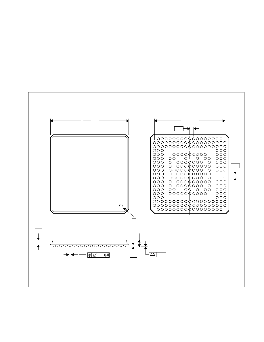
13≠1
13 Mechanical Information
The PCI7x20 is packaged in a 288-ball GHK BGA package. The following shows the mechanical dimensions for the
GHK package.
GHK (S-PBGA-N288)
PLASTIC BALL GRID ARRAY
0,08
0,12
1,40 MAX
0,85
0,45
0,55
0,35
0,45
0,95
15,90
SQ
16,10
Seating Plane
7
J
B
A
1
D
C
E
G
F
H
2
4
3
6
5
T
K
M
L
P
N
R
W
U
V
12
8
9
10
11
15
14
13
16
17
14,40 TYP
18
19
4145273-4/E 08/02
A1 Corner
0,80
0,80
Bottom View
NOTES: B. All linear dimensions are in millimeters.
C. This drawing is subject to change without notice.
D. MicroStar BGA
configuration.
MicroStar BGA is a trademark of Texas Instruments.

13≠2

IMPORTANT NOTICE
Texas Instruments Incorporated and its subsidiaries (TI) reserve the right to make corrections, modifications,
enhancements, improvements, and other changes to its products and services at any time and to discontinue
any product or service without notice. Customers should obtain the latest relevant information before placing
orders and should verify that such information is current and complete. All products are sold subject to TI's terms
and conditions of sale supplied at the time of order acknowledgment.
TI warrants performance of its hardware products to the specifications applicable at the time of sale in
accordance with TI's standard warranty. Testing and other quality control techniques are used to the extent TI
deems necessary to support this warranty. Except where mandated by government requirements, testing of all
parameters of each product is not necessarily performed.
TI assumes no liability for applications assistance or customer product design. Customers are responsible for
their products and applications using TI components. To minimize the risks associated with customer products
and applications, customers should provide adequate design and operating safeguards.
TI does not warrant or represent that any license, either express or implied, is granted under any TI patent right,
copyright, mask work right, or other TI intellectual property right relating to any combination, machine, or
process in which TI products or services are used. Information published by TI regarding third≠party products
or services does not constitute a license from TI to use such products or services or a warranty or endorsement
thereof. Use of such information may require a license from a third party under the patents or other intellectual
property of the third party, or a license from TI under the patents or other intellectual property of TI.
Reproduction of information in TI data books or data sheets is permissible only if reproduction is without
alteration and is accompanied by all associated warranties, conditions, limitations, and notices. Reproduction
of this information with alteration is an unfair and deceptive business practice. TI is not responsible or liable for
such altered documentation.
Resale of TI products or services with statements different from or beyond the parameters stated by TI for that
product or service voids all express and any implied warranties for the associated TI product or service and
is an unfair and deceptive business practice. TI is not responsible or liable for any such statements.
Following are URLs where you can obtain information on other Texas Instruments products and application
solutions:
Products
Applications
Amplifiers
amplifier.ti.com
Audio
www.ti.com/audio
Data Converters
dataconverter.ti.com
Automotive
www.ti.com/automotive
DSP
dsp.ti.com
Broadband
www.ti.com/broadband
Interface
interface.ti.com
Digital Control
www.ti.com/digitalcontrol
Logic
logic.ti.com
Military
www.ti.com/military
Power Mgmt
power.ti.com
Optical Networking
www.ti.com/opticalnetwork
Microcontrollers
microcontroller.ti.com
Security
www.ti.com/security
Telephony
www.ti.com/telephony
Video & Imaging
www.ti.com/video
Wireless
www.ti.com/wireless
Mailing Address: Texas Instruments
Post Office Box 655303 Dallas, Texas 75265
Copyright
2003, Texas Instruments Incorporated