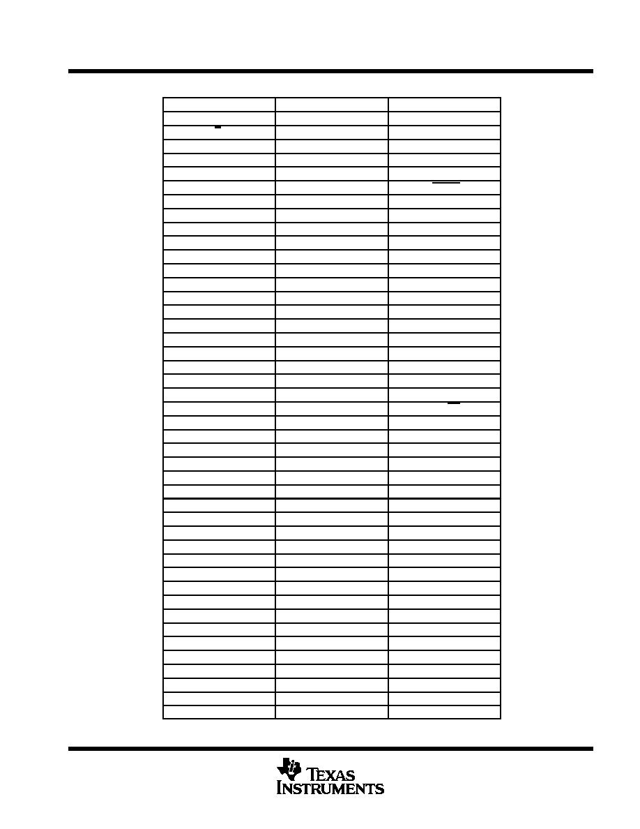
 | –≠–ª–µ–∫—Ç—Ä–æ–Ω–Ω—ã–π –∫–æ–º–ø–æ–Ω–µ–Ω—Ç: PCI930PBK | –°–∫–∞—á–∞—Ç—å:  PDF PDF  ZIP ZIP |
PCI930
3-TO-1 ZOOMED VIDEO SWITCH
SCPS018B ≠ OCTOBER 1997 ≠ REVISED DECEMBER 1997
1
POST OFFICE BOX 655303
∑
DALLAS, TEXAS 75265
D
Zoomed Video Switch ≠ Supports up to
3 ZV Sources
D
Designed for Use With the TI
TM
PCI1220/1221 Leadership PC Card
Controllers
D
First two (2) ZV Inputs are Controlled by
PCI1220/1221 Control Signal Outputs
D
100% Compliant With the PCMCIA Zoomed
Video Standard
D
Status Bit Indicates ZV Activity ≠ Can be
Used to Switch a Fourth External ZV
Source
D
Switching can be Software Programmed
Using Registers in the PCI1220/1221
D
Low Power 3.3-Volt Core Logic
D
Small Form Factor 128-Pin TQFP Package
description
The 3-to-1 ZV switch is a companion chip to the PCI1220/1221 PC Card controllers; however, it can be used
in other applications where multiple ZV sources require external buffering. The ZV switch is a 3:1 multiplexer
for the 23 pins defined in the PCMCIA zoomed video interface. The ZV interface includes both the video and
audio data as defined by the
Zoomed Video Specification.
The three ZV source interfaces are referred to as A, B, and C. ZV sources A and B are intended for use with
the PCI1220/1221 PC Card zoom video outputs. The third source, C, may be from a variety of external ZV
sources.
An advanced CMOS process is used to achieve low system-power consumption.
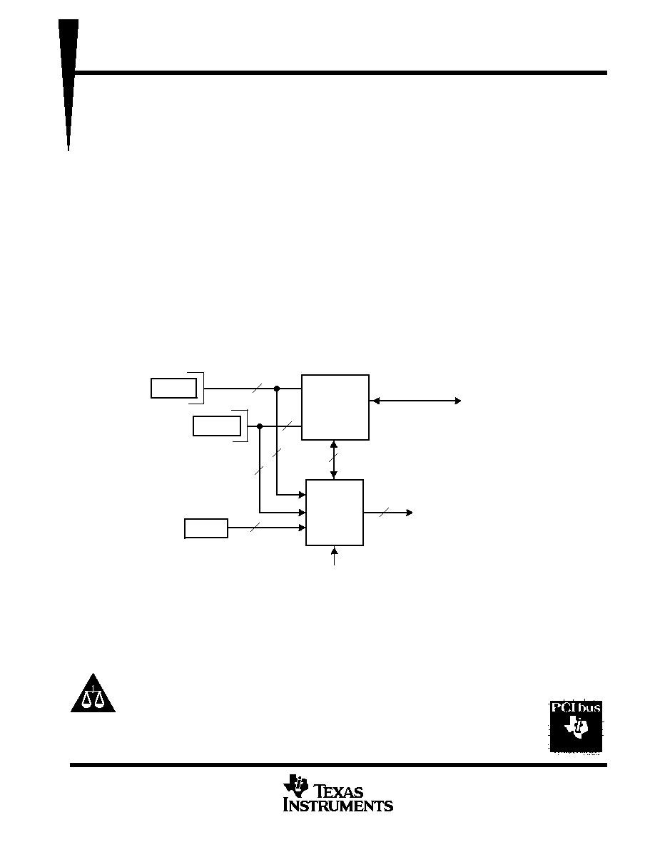
PCI1220
PC Card
Controller
PCI Bus
PC Card
TM
Socket A
PC Card
Socket B
23
23
PCI930
3-to-1 ZV
Switch
23
23
Third ZV
Source
2 Control Pins
ZV Output to VGA Controller
and Audio CODEC
NOTES:
1. The PC Card interface is 68 pins for CardBus and 16-bit PC Cards. In zoomed-video mode 23 pins are used for routing the
zoomed video signals too the VGA controller.
2. Control pin for third ZV source (Can Use GPO From PCI1220).
Control Pin
(See Note 2)
68
68
(See Note 1)
Figure 1. System-Level Diagram for PCI930 with the PCI1220 PC Card Controller
PC Card is a trademark of Personal Computer Memory Card International Association (PCMCIA).
TI is a trademark of Texas Instruments Incorporated.
Copyright
©
1997, Texas Instruments Incorporated
PRODUCTION DATA information is current as of publication date.
Products conform to specifications per the terms of Texas Instruments
standard warranty. Production processing does not necessarily include
testing of all parameters.
Please be aware that an important notice concerning availability, standard warranty, and use in critical applications of
Texas Instruments semiconductor products and disclaimers thereto appears at the end of this data sheet.
PCI930
3-TO-1 ZOOMED VIDEO SWITCH
SCPS018B ≠ OCTOBER 1997 ≠ REVISED DECEMBER 1997
2
POST OFFICE BOX 655303
∑
DALLAS, TEXAS 75265
functional block diagram
Source
A
Source
B
Source
C
Switch
Control
Switch
Circuit
23
23
Switch
output
23
PCI Card Sources
A_xx
B_xx
C_xx
A/B_STAT
A/B_SEL
C_STAT
ZV_OE
ZV_STAT
ZV_xx
23
RESET
PCI930
3-TO-1 ZOOMED VIDEO SWITCH
SCPS018B ≠ OCTOBER 1997 ≠ REVISED DECEMBER 1997
3
POST OFFICE BOX 655303
∑
DALLAS, TEXAS 75265
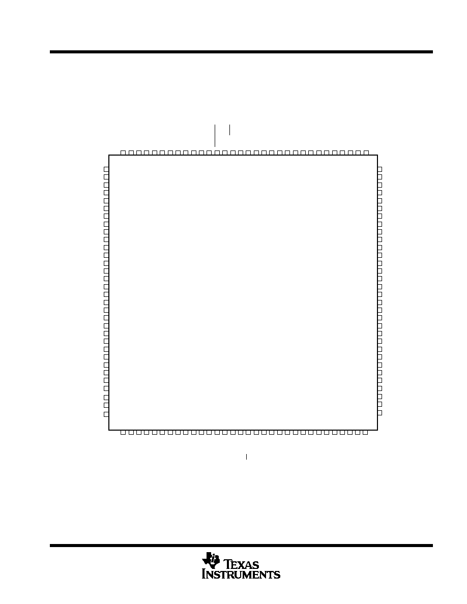
terminal assignments
1
2
3
4
5
6
7
8
9
10
11
12
13
14
15
16
17
18
19
20
21
22
23
24
25
26
27
28
29
101
102
96
95
94
93
92
91
90
89
88
87
86
85
84
83
82
81
80
79
78
77
76
75
74
73
72
71
70
69
68
61
60
59
58
57
56
55
54
53
52
51
50
49
48
47
46
45
44
43
42
41
40
39
38
37
36
35
34
33
99
100
62
30
67
NC
ZV_Y0
ZV_VSYNC
ZV_HREF
GND
GND
GND
C_PCLK
C_SDATA
C_MCLK
C_SCLK
GND
C_UV2
NC
GND
A_UV2
A_UV3
A_UV7
A_SCLK
A_MCLK
A_LRCLK
A_SDATA
A_PCLK
B_HREF
GND
B_VSYNC
B_Y0
B_UV0
NC
A_Y0
A_VSYNC
RESET
GND
GND
ZV_UV2
NC
C_UV0
B_UV2
B_UV3
GND
B_UV4
B_SCLK
B_MCLK
B_LRCLK
NC
B_SDA
T
A
B_PCLK
A/B_ST
A
T
C_ST
A
T
GND
C_VSYNC
C_Y0
V
CC
V
CC
V
CC
V
CC
CC
V
A/B_SEL
CC
V
PCI930
(TOP VIEW)
32
NC
31
63
64
97
98
ZV_UV1
NC
66
65
C_UV1
NC
103
104
105
106
107
108
109
11
0
111
11
2
11
3
11
4
11
5
11
6
11
7
11
8
11
9
120
121
122
123
124
125
126
127
128
A_UV0
A_UV1
V
CCS
A_UV4
A_UV5
A_UV6
B_Y1
B_Y2
B_Y3
B_Y4
B_Y5
B_Y6
B_Y7
B_UV1
CCS
V
B_UV5
B_UV6
B_UV7
C_HREF
C_Y1
C_Y2
C_Y3
C_Y4
C_Y5
C_Y6
C_Y7
V
CCS
C_UV3
C_UV4
C_UV5
C_UV6
C_UV7
C_LRCLK
ZV_Y1
ZV_Y2
ZV_Y3
ZV_Y4
ZV_Y5
ZV_Y6
ZV_Y7
ZV_UV0
CCS
V
ZV_UV3
ZV_UV4
ZV_UV5
ZV_UV6
ZV_UV7
ZV_SCLK
ZV_MCLK
CC
V
ZV_LRCLK
ZV_SDA
T
A
ZV_PCLK
ZV_ST
A
T
ZV_OE
A_HREF
CC
V
A_Y1
A_Y2
A_Y3
A_Y4
A_Y5
A_Y6
A_Y7
PCI930
3-TO-1 ZOOMED VIDEO SWITCH
SCPS018B ≠ OCTOBER 1997 ≠ REVISED DECEMBER 1997
4
POST OFFICE BOX 655303
∑
DALLAS, TEXAS 75265
Table 1. Terminal Assignments Sorted by Pin Number
TERMINAL
TERMINAL
TERMINAL
NO.
NAME
NO.
NAME
NO.
NAME
1
NC
44
B_LRCLK
87
ZV_Y1
2
A_UV0
45
VCC
88
ZV_Y2
3
A_UV1
46
B_SDATA
89
ZV_Y3
4
VCCS
47
B_PCLK
90
ZV_Y4
5
GND
48
A/B_STAT
91
VCC
6
A_UV2
49
A/B_SEL
92
ZV_Y5
7
A_UV3
50
C_STAT
93
ZV_Y6
8
A_UV4
51
GND
94
ZV_Y7
9
A_UV5
52
C_HREF
95
ZV_UV0
10
A_UV6
53
C_VSYNC
96
NC
11
A_UV7
54
C_Y0
97
NC
12
A_SCLK
55
C_Y1
98
ZV_UV1
13
VCC
56
C_Y2
99
VCCS
14
A_MCLK
57
C_Y3
100
ZV_UV2
15
A_LRCLK
58
C_Y4
101
GND
16
A_SDATA
59
VCC
102
ZV_UV3
17
A_PCLK
60
C_Y5
103
ZV_UV4
18
B_HREF
61
C_Y6
104
ZV_UV5
19
GND
62
C_Y7
105
ZV_UV6
20
B_VSYNC
63
C_UV0
106
ZV_UV7
21
B_Y0
64
NC
107
ZV_SCLK
22
B_Y1
65
NC
108
ZV_MCLK
23
B_Y2
66
C_UV1
109
VCC
24
B_Y3
67
VCCS
110
ZV_LRCLK
25
B_Y4
68
C_UV2
111
ZV_SDATA
26
B_Y5
69
GND
112
ZV_PCLK
27
VCC
70
C_UV3
113
ZV_STAT
28
B_Y6
71
C_UV4
114
ZV_OE
29
B_Y7
72
C_UV5
115
GND
30
B_UV0
73
C_UV6
116
RESET
31
B_UV1
74
C_UV7
117
A_HREF
32
NC
75
C_SCLK
118
A_VSYNC
33
NC
76
C_MCLK
119
A_Y0
34
VCCS
77
VCC
120
A_Y1
35
B_UV2
78
C_LRCLK
121
A_Y2
36
B_UV3
79
C_SDATA
122
A_Y3
37
GND
80
C_PCLK
123
VCC
38
B_UV4
81
GND
124
A_Y4
39
B_UV5
82
GND
125
A_Y5
40
B_UV6
83
GND
126
A_Y6
41
B_UV7
84
ZV_HREF
127
A_Y7
42
B_SCLK
85
ZV_VSYNC
128
NC
43
B_MCLK
86
ZV_Y0
***
***
PCI930
3-TO-1 ZOOMED VIDEO SWITCH
SCPS018B ≠ OCTOBER 1997 ≠ REVISED DECEMBER 1997
5
POST OFFICE BOX 655303
∑
DALLAS, TEXAS 75265
Table 2. Terminal Assignments Sorted by Pin Name
TERMINAL
TERMINAL
TERMINAL
NO.
NAME
NO.
NAME
NO.
NAME
49
A/B_SEL
24
B_Y3
65
NC
48
A/B_STAT
25
B_Y4
96
NC
117
A_HREF
26
B_Y5
97
NC
15
A_LRCLK
28
B_Y6
128
NC
14
A_MCLK
29
B_Y7
116
RESET
17
A_PCLK
52
C_HREF
13
VCC
12
A_SCLK
78
C_LRCLK
27
VCC
16
A_SDATA
76
C_MCLK
45
VCC
2
A_UV0
80
C_PCLK
59
VCC
3
A_UV1
75
C_SCLK
77
VCC
6
A_UV2
79
C_SDATA
91
VCC
7
A_UV3
50
C_STAT
109
VCC
8
A_UV4
63
C_UV0
123
VCC
9
A_UV5
66
C_UV1
4
VCCS
10
A_UV6
68
C_UV2
34
VCCS
11
A_UV7
70
C_UV3
67
VCCS
118
A_VSYNC
71
C_UV4
99
VCCS
119
A_Y0
72
C_UV5
84
ZV_HREF
120
A_Y1
73
C_UV6
110
ZV_LRCLK
121
A_Y2
74
C_UV7
108
ZV_MCLK
122
A_Y3
53
C_VSYNC
114
ZV_OE
124
A_Y4
54
C_Y0
112
ZV_PCLK
125
A_Y5
55
C_Y1
107
ZV_SCLK
126
A_Y6
56
C_Y2
111
ZV_SDATA
127
A_Y7
57
C_Y3
113
ZV_STAT
18
B_HREF
58
C_Y4
85
ZV_VSYNC
44
B_LRCLK
60
C_Y5
95
ZV_UV0
43
B_MCLK
61
C_Y6
98
ZV_UV1
47
B_PCLK
62
C_Y7
100
ZV_UV2
42
B_SCLK
5
GND
102
ZV_UV3
46
B_SDATA
19
GND
103
ZV_UV4
30
B_UV0
37
GND
104
ZV_UV5
31
B_UV1
51
GND
105
ZV_UV6
35
B_UV2
69
GND
106
ZV_UV7
36
B_UV3
81
GND
86
ZV_Y0
38
B_UV4
82
GND
87
ZV_Y1
39
B_UV5
83
GND
88
ZV_Y2
40
B_UV6
101
GND
89
ZV_Y3
41
B_UV7
115
GND
90
ZV_Y4
20
B_VSYNC
1
NC
92
ZV_Y5
21
B_Y0
32
NC
93
ZV_Y6
22
B_Y1
33
NC
94
ZV_Y7
23
B_Y2
64
NC
***
***
PCI930
3-TO-1 ZOOMED VIDEO SWITCH
SCPS018B ≠ OCTOBER 1997 ≠ REVISED DECEMBER 1997
6
POST OFFICE BOX 655303
∑
DALLAS, TEXAS 75265
Table 3. ZV Switch Control and Status Terminals
TERMINAL
TYPE
FUNCTION
NAME
NO.
TYPE
FUNCTION
RESET
116
I
Chip reset. When asserted (driven low), the chip three-states all outputs. In addition, the PCI930
checks for a pullup resistor on the A/B STAT pin as denoted under ZV_xx terminal function.
A/B_STAT
48
I
PC Card ZV (Socket 0 or 1) active. This input indicates that either the A or B source from the PC Card
controller is active. This signal is used with A/B_SEL to determine which socket ZV source drives the
ZV_xx outputs. The A or B source can be passed to ZV_xx if the C source is either of lower precedence,
or is not sourcing valid ZV data, as indicated by the C_STAT signal.
A/B_SEL
49
I
Socket A/B select. When this pin and A/B_STAT are high, the PC Card socket A ZV data is valid. When
this pin is low, and the A/B_STAT input is high, the PC Card socket B ZV data is valid. This input has
no meaning if the A/B_STAT input is low.
C_STAT
50
I
C source status. When this input is high, the ZV source from interface C is valid, and can be driven
to the ZV_xx outputs. The C source can be passed to ZV_xx if the A and B sources are either of lower
precedence, or A or B is not sourcing valid ZV data.
ZV_OE
114
I
ZV output I/F enable. When this terminal is low, the ZV switch drives the ZV_xx terminals.
ZV_STAT
113
O
ZV output status. This terminal is driven high when the ZV switch drives the ZV_xx terminals.
ZV_xx State
N/A
N/A
When a pullup resistor is present on the A/B_STAT pin during RESET, then the ZV_xx interface is
three-stated if the ZV_xx interface is inactive. During the default state, no pullup resistor, a reset drives
the ZV_xx interface to a logic low state when inactive.
PCI930
3-TO-1 ZOOMED VIDEO SWITCH
SCPS018B ≠ OCTOBER 1997 ≠ REVISED DECEMBER 1997
7
POST OFFICE BOX 655303
∑
DALLAS, TEXAS 75265
Terminal Functions
Table 4. Power Supply Terminal Functions
TERMINAL
TYPE
FUNCTION
NAME
NO.
TYPE
FUNCTION
GND
5, 19, 51, 69, 81, 82, 83, 101, 115
I
Device ground terminals.
VCC
13, 27, 45, 59, 77, 91, 109, 123
I
3.3V power supply input for core.
VCCS
4, 34, 67, 99
I
Rail input for 5V tolerance on zoom video streams
Table 5. ZV Stream Interface
TERMINAL
TYPE
FUNCTION
NAME
NO.
TYPE
FUNCTION
HREF
18, 52, 84, 117
Horizontal sync to ZV port.
VSYNC
20, 53, 85, 118
Vertical sync to ZV port.
Y7:0
A_ = 127, 126, 125, 124, 122, 121, 120, 119
B_ = 29, 28, 26, 25, 24, 23, 22, 21
C_ = 62, 61, 60, 58, 57, 56, 55, 54
ZV_ = 94, 93, 92, 90, 89, 88, 87, 86
I
I
I
O
Video data to ZV port YUV:4:2:2 format.
Video data to ZV port YUV:4:2:2 format.
Video data to ZV port YUV:4:2:2 format.
Video data YUV:4:2:2 format.
UV7:0
A_ = 11, 10, 9, 8, 7, 6, 3, 2
B_ = 41, 40, 39, 38, 36, 35, 31, 30
C_ = 74, 73, 72, 71, 70, 68, 66, 63
ZV_ = 106, 105, 104, 103, 102, 100, 98, 95
I
I
I
O
Video data to ZV port YUV:4:2:2 format.
Video data to ZV port YUV:4:2:2 format.
Video data to ZV port YUV:4:2:2 format.
Video data YUV:4:2:2 format.
SCLK
12, 42, 75, 107
Audio SCLK PCM signal.
MCLK
14, 43, 76, 108
Audio MCLK PCM signal.
PCLK
17, 47, 80, 112
Pixel clock to ZV port.
LRCLK
15, 44, 78, 110
Audio LRCLK PCM signal.
SDATA
16, 46, 79, 111
Audio PCM data signal.
Inputs on A, B, and C source ports; Outputs to ZV_xx interface
control settings for ZV switch routing
Table 6 lists termination conditions that can exercise control over the ZV switch and shows the results.
Table 6. Termination Conditions
FUNCTION
CONDITION
RESULT
ZV xx inactive state
Pullup resistor on A/B_STAT
ZV_xx three-stated
ZV_xx inactive state
No pullup resistor on A/B_STAT
ZV_xx driven L
C precedence control
Pullup resistor on A/B_SEL
C takes precedence over A/B.
C precedence control
No pullup resistor on A/B_SEL
A/B takes precedence over C.
PCI930
3-TO-1 ZOOMED VIDEO SWITCH
SCPS018B ≠ OCTOBER 1997 ≠ REVISED DECEMBER 1997
8
POST OFFICE BOX 655303
∑
DALLAS, TEXAS 75265
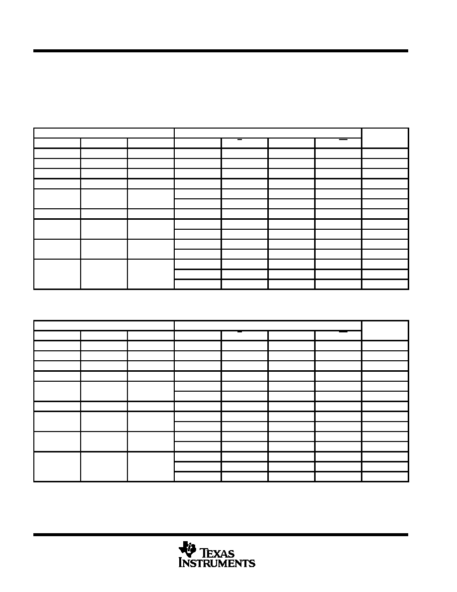
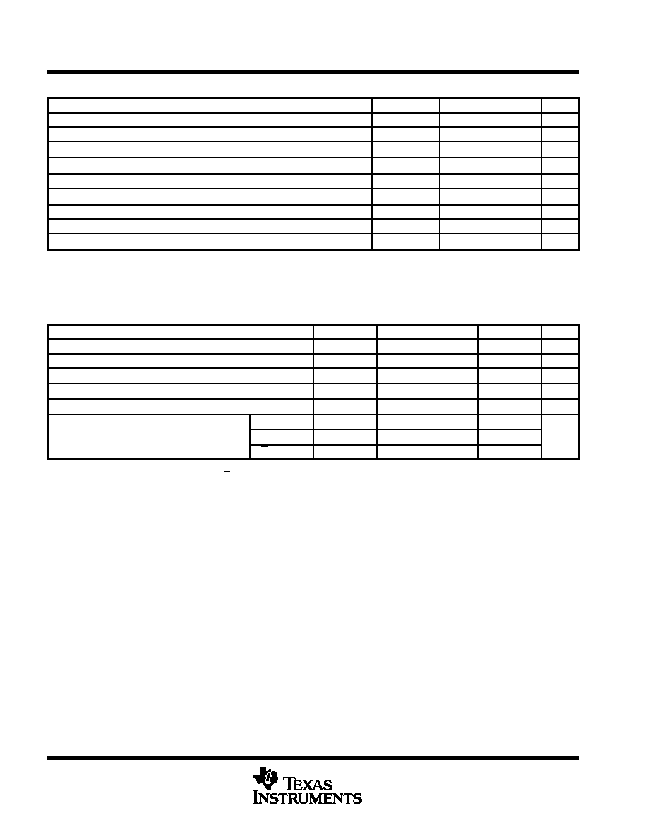
Table 7 and Table 8 define the control settings that allow the PCI930 to route the ZV data from the three inputs
(A_xx, B_xx, or C_xx) to the output (ZV_xx). The Tables are separated based upon the configuration of the
PCI930.
D
Table 7:
Output when inputs A/B have precedence over C
D
Table 8:
Output when input C has precedence over A/B
Table 7. Output When Inputs A/B Have Precedence Over Input C
INPUTS
CONTROL SETTINGS
OUTPUT
A_XX
B_XX
C_XX
A/B_STAT
A/B_SEL
C_STAT
ZV_OE
at ZV_xx
X
X
X
X
X
X
1
Non ZV data
Non ZV data
Non ZV data
0
X
0
X
Non ZV data
Non ZV data
ZV data
0
X
1
X
C_xx
Non ZV data
ZV data
Non ZV data
1
0
X
0
B_xx
Non ZV data
ZV data
ZV data
1
0
X
0
B_xx
Non ZV data
ZV data
ZV data
0
X
1
0
C_xx
ZV data
Non ZV data
Non ZV data
1
1
X
0
A_xx
ZV data
Non ZV data
ZV data
1
1
X
0
A_xx
ZV data
Non ZV data
ZV data
0
X
1
0
C_xx
ZV data
ZV data
Non ZV data
1
1
X
0
A_xx
ZV data
ZV data
Non ZV data
1
0
X
0
B_xx
1
1
X
0
A_xx
ZV data
ZV data
ZV data
1
0
X
0
B_xx
0
X
1
0
C_xx
Inactive state
Table 8. Output When Input C Has Precedence Over A/B
INPUTS
CONTROL SETTINGS
OUTPUT
A_XX
B_XX
C_XX
A/B_STAT
A/B_SEL
C_STAT
ZV_OE
at ZV_xx
X
X
X
X
X
X
1
Non ZV data
Non ZV data
Non ZV data
0
X
0
X
Non ZV data
Non ZV data
ZV data
X
X
1
0
C_xx
Non ZV data
ZV data
Non ZV data
1
0
0
0
B_xx
Non ZV data
ZV data
ZV data
1
0
0
0
B_xx
Non ZV data
ZV data
ZV data
X
X
1
0
C_xx
ZV data
Non ZV data
Non ZV data
1
1
0
0
A_xx
ZV data
Non ZV data
ZV data
1
1
0
0
A_xx
ZV data
Non ZV data
ZV data
X
X
1
0
C_xx
ZV data
ZV data
Non ZV data
1
1
0
0
A_xx
ZV data
ZV data
Non ZV data
1
0
0
0
B_xx
1
1
0
0
A_xx
ZV data
ZV data
ZV data
1
0
0
0
B_xx
X
X
1
0
C_xx
Inactive state
PCI930
3-TO-1 ZOOMED VIDEO SWITCH
SCPS018B ≠ OCTOBER 1997 ≠ REVISED DECEMBER 1997
9
POST OFFICE BOX 655303
∑
DALLAS, TEXAS 75265
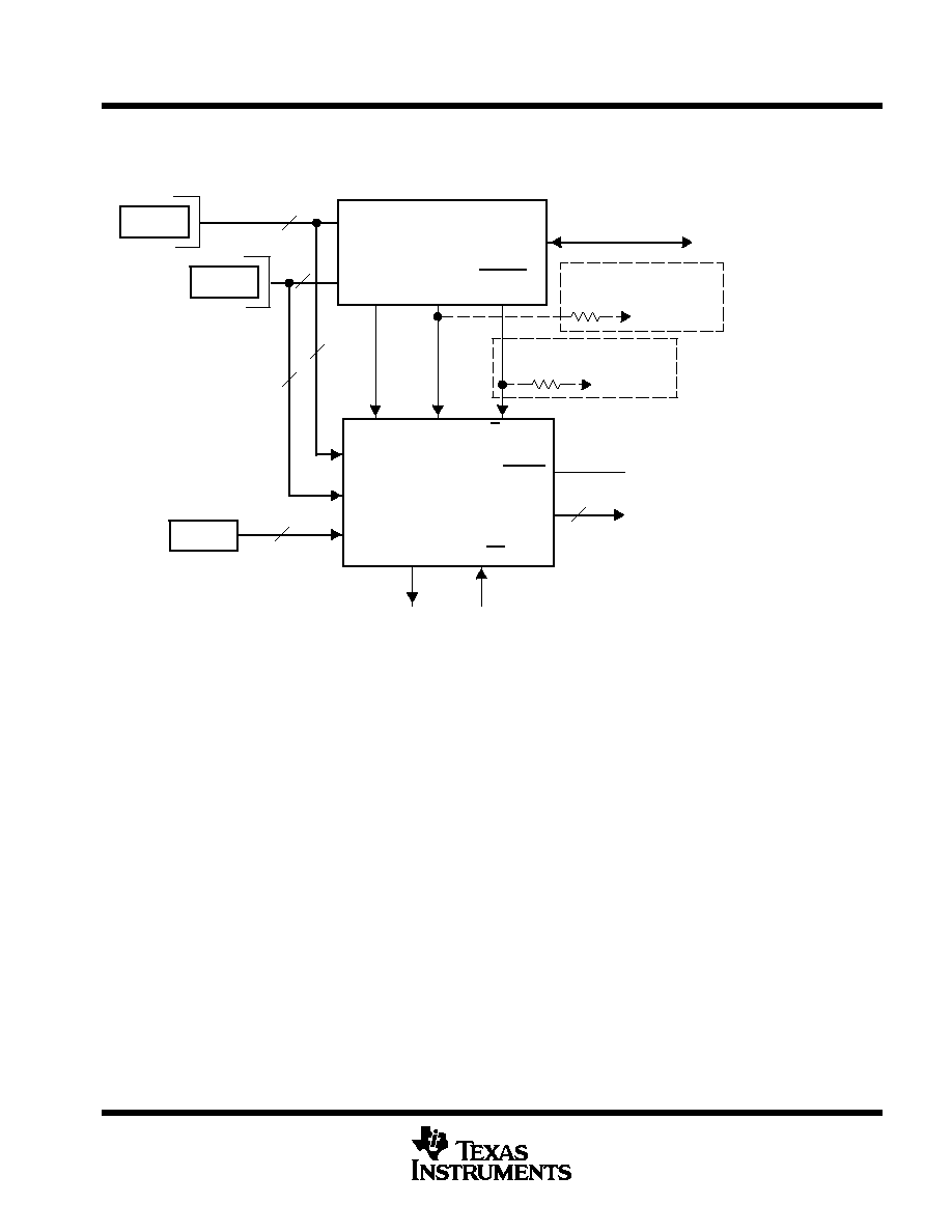
typical system configuration with PCI1220 PC Card controller
PCI1220
PCI Bus
PC Card
Socket A
PC Card
Socket B
23
23
PCI930
23
23
Third
ZV
Source
ZV Output to VGA Controller
and Audio CODEC
System Reset Control
Optional Pullup to Set
ZV_xx Inactive
VCC
Optional Pullup to Set
C Precedence
VCC
MFUNC5
GPO4
(160)
MFUNC2
ZVSTAT
(157)
MFUNC4
ZVSEL1
(159)
C_STAT
A/B_STAT A/B_SEL
A_xx
B_xx
C_xx
ZV_STAT
AZ_OE
ZV
Status
Pin
ZV_xx
Output
Enable
ZV_xx
RESET
68
68
Figure 2. Typical System Configuration for PCI930 With TI PCI1220 PC Card Controller
absolute maximum ratings over operating free-air temperature range (unless otherwise noted)
Supply voltage range, V
CC
≠0.5 V to 6 V
. . . . . . . . . . . . . . . . . . . . . . . . . . . . . . . . . . . . . . . . . . . . . . . . . . . . . . . . . .
Supply voltage range, V
CCS
≠0.5 V to 6 V
. . . . . . . . . . . . . . . . . . . . . . . . . . . . . . . . . . . . . . . . . . . . . . . . . . . . . . . . .
Input voltage range, V
I
≠0.5 V to 6.5 V
. . . . . . . . . . . . . . . . . . . . . . . . . . . . . . . . . . . . . . . . . . . . . . . . . . . . . . . . . . . . .
Output voltage range, V
O
≠0.5 V to V
CC
+ 0.5 V
. . . . . . . . . . . . . . . . . . . . . . . . . . . . . . . . . . . . . . . . . . . . . . . . . . . .
Input Clamp Current, I
IK
(V
I
< 0 or V
I
> V
CC
) (see Note 3)
±
20 mA
. . . . . . . . . . . . . . . . . . . . . . . . . . . . . . . . . . . .
Output Clamp Current, I
OK
(V
O
< 0 or V
O
> V
CC
) (see Note 4)
±
20 mA
. . . . . . . . . . . . . . . . . . . . . . . . . . . . . . .
Storage temperature range
≠65
∞
C to 150
∞
C
. . . . . . . . . . . . . . . . . . . . . . . . . . . . . . . . . . . . . . . . . . . . . . . . . . . . . . . .
Virtual junction temperature, T
J
150
∞
C
. . . . . . . . . . . . . . . . . . . . . . . . . . . . . . . . . . . . . . . . . . . . . . . . . . . . . . . . . . . .
Stresses beyond those listed under "absolute maximum ratings" may cause permanent damage to the device. These are stress ratings only, and
functional operation of the device at these or any other conditions beyond those indicated under "recommended operating conditions" is not
implied. Exposure to absolute-maximum-rated conditions for extended periods may affect device reliability.
NOTES:
3. Applies for external input and bidirectional buffers. VI > VCC does not apply to fail-safe terminals. ZV terminals are measured with
respect to VCCS. The limit specified applies for a DC condition.
4. Applies for external output and bidirectional buffers. VO > VCC does not apply to fail-safe terminals. ZV terminals are measured with
respect to VCCS. The limit specified applies for a DC condition.
PCI930
3-TO-1 ZOOMED VIDEO SWITCH
SCPS018B ≠ OCTOBER 1997 ≠ REVISED DECEMBER 1997
10
POST OFFICE BOX 655303
∑
DALLAS, TEXAS 75265
recommended operating conditions (see Note 5)
PARAMETER
OPERATION
MIN
NOM
MAX
UNIT
VCC
Core voltage ≠ Commercial
3.3 V
3
3.3
3.6
V
VCCS
I/O voltage ≠ Commercial
5 V
4.75
5
5.25
V
VIH
High-level input voltage
2
VCCS
V
VIL
Low-level input voltage
0
0.8
V
VI
Input voltage
0
VCCS
V
VO
Output voltage
0
VCCS
V
tt
Input transition (rise and fall) time, see Figure 3
0
25
ns
TA
Operating ambient temperature range
0
25
70
∞
C
TJ
Virtual junction temperatureß
0
25
115
∞
C
NOTE 5: Unused or floating pins (input or I/O) must be held high or low.
Applies for external input and bidirectional buffers without hysteresis
Applies for external output buffers.
ß These junction temperatures reflect simulation conditions. Customer is responsible for verifying junction temperature.
electrical characteristics over recommended operating conditions (unless otherwise noted)
PARAMETER
OPERATION
TEST CONDITIONS
MIN
MAX
UNIT
VOH
High-level output voltage
IOH = ≠3.6 mA
2.15
V
VOL
Low-level output voltage
IOL = 6.48 mA
0.5
V
IOZL
3-state-output Hi-Z current∂
5.5 V
VI = GND
≠10
µ
A
IOZH
3-state-output Hi-Z current∂
5.5 V
VI = VCC
10
µ
A
IIL
Low-level input current#
VI = GND
≠1
µ
A
input pins
5.5 V
VI = VCC
1
IIH
High-level input current
A/B_STAT
5.0 V
VI = 3.0 V
230
µ
A
A/B_SEL
5.0 V
VI = 3.0 V
230
∂ IOZ is not tested on ZV_STAT(pin 113) due to no Z state.
# IIL is not tested on A/B_STAT (pin 48), and A/B_SEL (pin 49) due to internal pulldown resistor.
PCI930
3-TO-1 ZOOMED VIDEO SWITCH
SCPS018B ≠ OCTOBER 1997 ≠ REVISED DECEMBER 1997
11
POST OFFICE BOX 655303
∑
DALLAS, TEXAS 75265
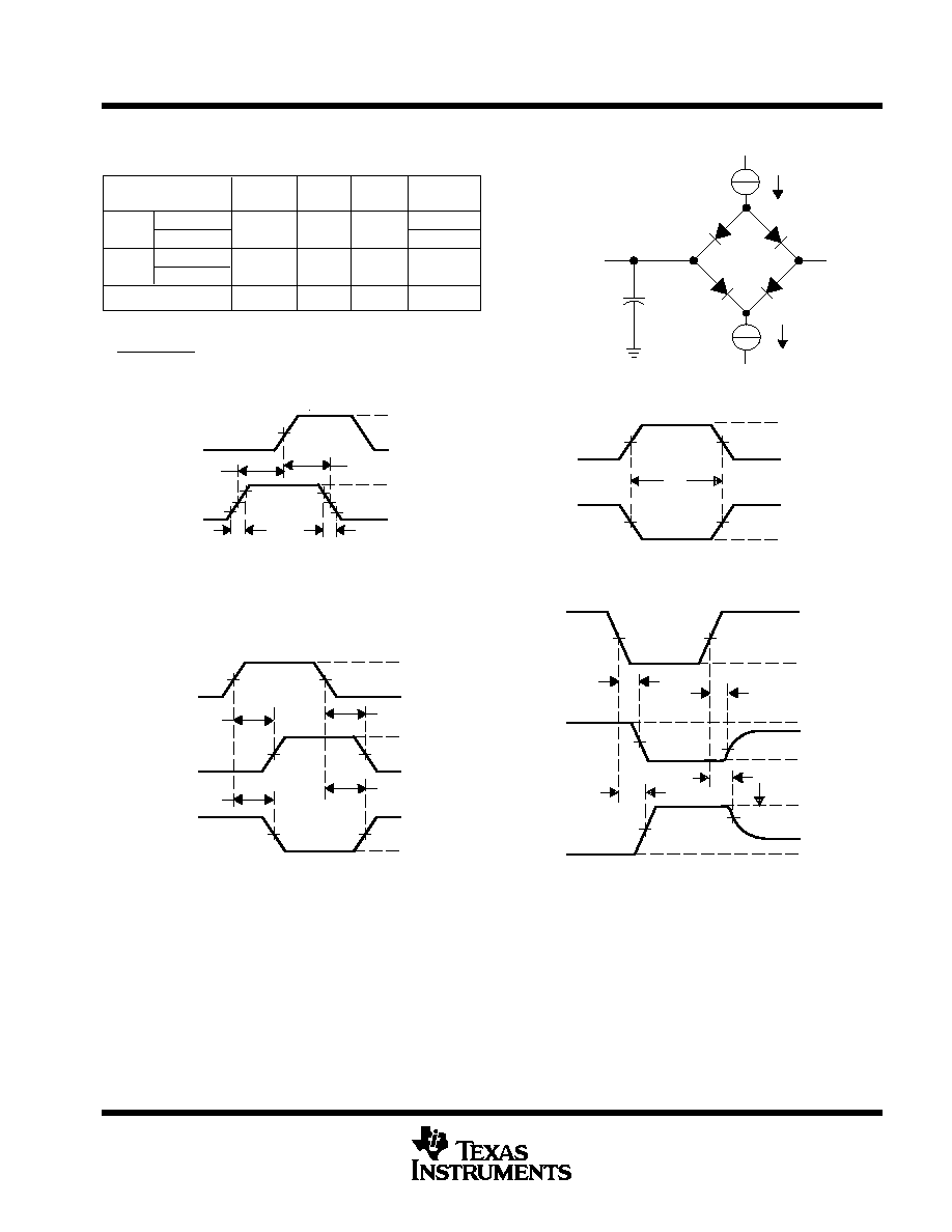
PARAMETER MEASUREMENT INFORMATION
CLOAD includes the typical load-circuit distributed capacitance
CLOAD
Test
Point
Timing
Input
(see Note A)
Out-of-Phase
Output
tpd
50% VCC
50% VCC
VCC
0 V
0 V
0 V
0 V
0 V
VOL
th
tsu
VOH
VOH
VOL
High-Level
Input
Low-Level
Input
tw
VOLTAGE WAVEFORMS
PROPAGATION DELAY TIMES
LOAD CIRCUIT
VOLTAGE WAVEFORMS
SETUP AND HOLD TIMES
INPUT RISE AND FALL TIMES
VOLTAGE WAVEFORMS
PULSE DURATION
tpd
tpd
tpd
VLOAD
IOH
IOL
From Output
Under Test
90% VCC
10% VCC
tf
tr
Output
Control
(low-level
enabling)
Waveform 1
(see Notes
B and C)
Waveform 2
(see Notes
B and C)
VOL
VOH
VOH ≠ 0.3 V
tPZL
tPZH
tPLZ
tPHZ
VOLTAGE WAVEFORMS
ENABLE AND DISABLE TIMES, 3-STATE OUTPUTS
VOL + 0.3 V
0 V
0 V
50% VCC
50% VCC
ten
tdis
tpd
tPZH
tPZL
tPHZ
tPLZ
CLOAD
(pF)
IOL
(mA)
TIMING
PARAMETER
50
8
≠8
0
3
1.5
50
8
8
≠8
≠8
LOAD CIRCUIT PARAMETERS
= 50
, where VOL = 0.6 V, IOL = 8 mA
IOL
50
VLOAD ≠ VOL
IOH
(mA)
VLOAD
(V)
Data
Input
In-Phase
Output
Input
(see Note A)
VCC
VCC
VCC
50% VCC
50% VCC
50% VCC
50% VCC
VCC
VCC
50% VCC
50% VCC
50% VCC
50% VCC
VCC
50% VCC
50% VCC
50% VCC
50% VCC
50% VCC
50% VCC
NOTES: A. Phase relationships between waveforms were chosen arbitrarily. All input pulses are supplied by pulse generators having the
following characteristics: PRR = 1 MHz, ZO = 50
, tr = 6 ns.
B. Waveform 1 is for an output with internal conditions such that the output is low except when disabled by the output control.
Waveform 2 is for an output with internal conditions such that the output is high except when disabled by the output control.
C. For tPLZ and tPHZ, VOL and VOH are measured values.
50% VCC
Figure 3. Load Circuit and Voltage Waveforms
PCI930
3-TO-1 ZOOMED VIDEO SWITCH
SCPS018B ≠ OCTOBER 1997 ≠ REVISED DECEMBER 1997
12
POST OFFICE BOX 655303
∑
DALLAS, TEXAS 75265
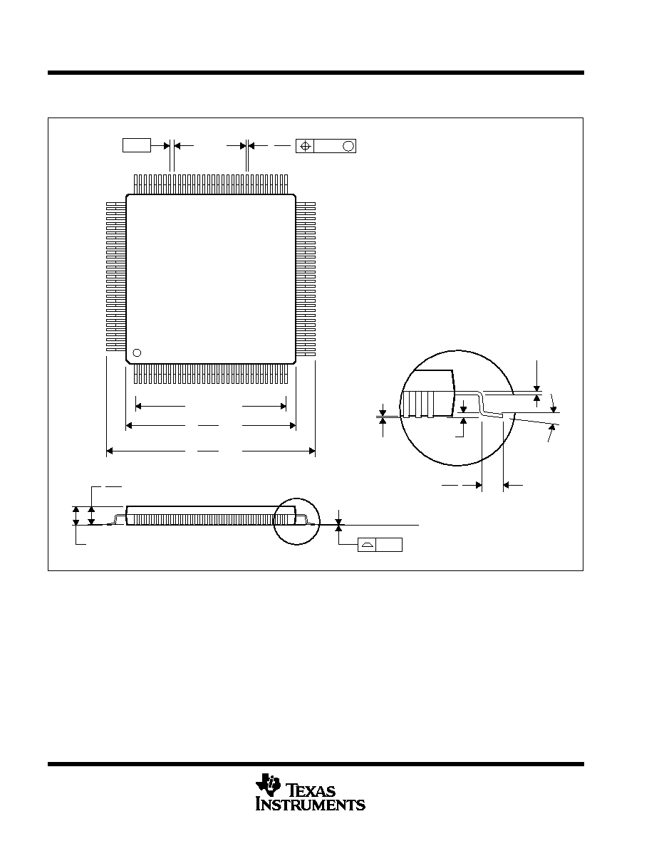
MECHANICAL DATA
PBK (S-PQFP-G128)
PLASTIC QUAD FLATPACK
4040279-3 / C 11/96
64
33
Gage Plane
0,13 NOM
0,25
0,45
0,75
Seating Plane
0,05 MIN
0,23
65
32
96
1
12,40 TYP
0,13
97
128
SQ
SQ
13,80
16,20
15,80
1,60 MAX
1,45
1,35
14,20
0
∞
≠ 7
∞
0,08
0,40
M
0,07
NOTES: D. All linear dimensions are in millimeters.
E. This drawing is subject to change without notice.
F. Falls within JEDEC MS-026

IMPORTANT NOTICE
Texas Instruments and its subsidiaries (TI) reserve the right to make changes to their products or to discontinue
any product or service without notice, and advise customers to obtain the latest version of relevant information
to verify, before placing orders, that information being relied on is current and complete. All products are sold
subject to the terms and conditions of sale supplied at the time of order acknowledgement, including those
pertaining to warranty, patent infringement, and limitation of liability.
TI warrants performance of its semiconductor products to the specifications applicable at the time of sale in
accordance with TI's standard warranty. Testing and other quality control techniques are utilized to the extent
TI deems necessary to support this warranty. Specific testing of all parameters of each device is not necessarily
performed, except those mandated by government requirements.
CERTAIN APPLICATIONS USING SEMICONDUCTOR PRODUCTS MAY INVOLVE POTENTIAL RISKS OF
DEATH, PERSONAL INJURY, OR SEVERE PROPERTY OR ENVIRONMENTAL DAMAGE ("CRITICAL
APPLICATIONS"). TI SEMICONDUCTOR PRODUCTS ARE NOT DESIGNED, AUTHORIZED, OR
WARRANTED TO BE SUITABLE FOR USE IN LIFE-SUPPORT DEVICES OR SYSTEMS OR OTHER
CRITICAL APPLICATIONS. INCLUSION OF TI PRODUCTS IN SUCH APPLICATIONS IS UNDERSTOOD TO
BE FULLY AT THE CUSTOMER'S RISK.
In order to minimize risks associated with the customer's applications, adequate design and operating
safeguards must be provided by the customer to minimize inherent or procedural hazards.
TI assumes no liability for applications assistance or customer product design. TI does not warrant or represent
that any license, either express or implied, is granted under any patent right, copyright, mask work right, or other
intellectual property right of TI covering or relating to any combination, machine, or process in which such
semiconductor products or services might be or are used. TI's publication of information regarding any third
party's products or services does not constitute TI's approval, warranty or endorsement thereof.
Copyright
©
1998, Texas Instruments Incorporated