24-Bit, 96kHz Sampling, 6-Channel,
Enhanced Multi-Level, Delta-Sigma
DIGITAL-TO-ANALOG CONVERTER
PCM1600
PCM1601
Æ
TM
DESCRIPTION
The PCM1600
(1)
and PCM1601
(1)
are CMOS mono-
lithic integrated circuits which feature six 24-bit audio
digital-to-analog converters and support circuitry in
either a LQFP-48 or MQFP-48 package. The digital-
to-analog converters utilize Burr-Brown's enhanced
multi-level, delta-sigma architecture, which employ
4th-order noise shaping and 8-level amplitude quanti-
zation to achieve excellent signal-to-noise performance
and a high tolerance to clock jitter.
The PCM1600 and PCM1601 accept industry-stan-
dard audio data formats with 16- to 24-bit audio data.
Sampling rates up to 100kHz are supported. A full set
of user-programmable functions are accessible through
a 4-wire serial control port which supports register
write and readback functions.
FEATURES
q
24-BIT RESOLUTION
q
ANALOG PERFORMANCE:
Dynamic Range: 105dB typ
SNR: 104dB typ
THD+N: 0.0018% typ
Full-Scale Output: 3.1Vp-p typ
q
8x OVERSAMPLING INTERPOLATION FILTER:
Stopband Attenuation: ≠82dB
Passband Ripple:
±
0.002dB
q
SAMPLING FREQUENCY: 10kHz to 100kHz
q
ACCEPTS 16, 18, 20, AND 24-BIT AUDIO DATA
q
DATA FORMATS: Standard, I
2
S, and Left-Justified
q
SYSTEM CLOCK: 256f
S
, 384f
S
, 512f
S
, or 768f
S
q
USER-PROGRAMMABLE FUNCTIONS:
Digital Attenuation: 0dB to ≠63dB, 0.5dB/Step
Soft Mute
Zero Detect Mute
Zero Flags for Each Output Channel
Digital De-Emphasis
Digital Filter Roll-Off: Sharp or Slow
q
DUAL SUPPLY OPERATION:
+5V Analog, +3.3V Digital
q
5V TOLERANT DIGITAL LOGIC INPUTS
q
PACKAGES
(1)
: LQFP-48 (PCM1600)
and MQFP-48 (PCM1601)
© 1999 Burr-Brown Corporation
PDS-1523C
Printed in U.S.A. March, 2000
APPLICATIONS
q
INTEGRATED A/V RECEIVERS
q
DVD MOVIE AND AUDIO PLAYERS
q
HDTV RECEIVERS
q
CAR AUDIO SYSTEMS
q
DVD ADD-ON CARDS FOR HIGH-END PCs
q
DIGITAL AUDIO WORKSTATIONS
q
OTHER MULTI-CHANNEL AUDIO SYSTEMS
International Airport Industrial Park ∑ Mailing Address: PO Box 11400, Tucson, AZ 85734 ∑ Street Address: 6730 S. Tucson Blvd., Tucson, AZ 85706 ∑ Tel: (520) 746-1111
Twx: 910-952-1111 ∑ Internet: http://www.burr-brown.com/ ∑ Cable: BBRCORP ∑ Telex: 066-6491 ∑ FAX: (520) 889-1510 ∑ Immediate Product Info: (800) 548-6132
NOTE: (1) The PCM1600 and PCM1601 utilize the same die and are
electrically the same. All references to the PCM1600 apply equally
to the PCM1601.
For most current data sheet and other product
information, visit www.burr-brown.com
PCM1601
PCM1600
SBAS116
Æ
2
PCM1600, PCM1601
SPECIFICATIONS
All specifications at +25
∞
C, +V
CC
= +5V, +V
DD
= +3.3V, system clock = 384f
S
(f
S
= 44.1kHz) and 24-bit data, unless otherwise noted.
PCM1600Y, PCM1601Y
PARAMETER
CONDITIONS
MIN
TYP
MAX
UNITS
RESOLUTION
24
Bits
DATA FORMAT
Audio Data Interface Formats
User Selectable
Standard, I
2
S, Left-Justified
Data Bit Length
User Selectable
16, 18, 20, 24-Bit
Audio Data Format
MSB-First, Binary Two's Complement
Sampling Frequency (f
S
)
10
100
kHz
System Clock Frequency
256, 384, 512, 768f
S
DIGITAL INPUT/OUTPUT
Logic Family
TTL-Compatible
Input Logic Level
V
IH
2.0
V
V
IL
0.8
V
Input Logic Current
I
IH
(1)
V
IN
= V
DD
0.1
µ
A
I
IL
(1)
V
IN
= 0V
≠0.1
µ
A
I
IH
(2)
V
IN
= V
DD
65
100
µ
A
I
IL
(2)
V
IN
= 0V
≠0.1
µ
A
Output Logic Level
V
OH
(3)
I
OH
= ≠2mA
2.4
V
V
OL
(3)
I
OL
= +2mA
1.0
V
V
OH
(4)
I
OH
= ≠4mA
2.4
V
V
OL
(4)
I
OL
= +4mA
1.0
V
DYNAMIC PERFORMANCE
(5)
THD+N, V
OUT
= 0dB
f
S
= 44.1kHz
0.0018
0.0045
%
f
S
= 96kHz
0.0035
%
V
OUT
= ≠60dB
f
S
= 44.1kHz
0.65
%
f
S
= 96kHz
0.75
%
Dynamic Range
EIAJ, A-Weighted, f
S
=44.1kHz
100
105
dB
A-Weighted, f
S
= 96kHz
104
dB
Signal-to-Noise Ratio
(6)
EIAJ, A-Weighted, f
S
=44.1kHz
98
104
dB
A-Weighted, f
S
= 96kHz
103
dB
Channel Separation
f
S
= 44.1kHz
96
102
dB
f
S
= 96kHz
101
dB
Level Linearity Error
V
OUT
= ≠90dB
±
0.5
dB
DC ACCURACY
Gain Error
±
1.0
% of FSR
Gain Mismatch, Channel-to-Channel
±
1.0
% of FSR
Bipolar Zero Error
V
O
= 0.5V
CC
at Bipolar Zero
±
30
mV
ANALOG OUTPUT
Output Voltage
Full Scale (0dB)
62% of V
CC
Vp-p
Center Voltage
50% V
CC
V
Load Impedance
AC Load
5
k
DIGITAL FILTER PERFORMANCE
Filter Characteristics 1, Sharp Roll-Off
Passband
±
0.002dB
0.454f
S
Hz
≠3dB
0.490f
S
Hz
Stopband
0.546f
S
Hz
Passband Ripple
±
0.002
dB
Stopband Attenuation
Stopband = 0.546f
S
≠75
dB
Stopband = 0.567f
S
≠82
dB
Filter Characteristics 2, Slow Roll-Off
Passband
±
0.002dB
0.274f
S
Hz
≠3dB
0.454f
S
Hz
Stopband
0.732f
S
Hz
Passband Ripple
±
0.002
dB
Stopband Attenuation
Stopband = 0.732f
S
≠82
dB
Delay Time
34/f
S
sec
De-Emphasis Error
±
0.1
dB
ANALOG FILTER PERFORMANCE
Frequency Response
f = 20kHz
≠0.03
dB
f = 44kHz
≠0.20
dB
Æ
3
PCM1600, PCM1601
The information provided herein is believed to be reliable; however, BURR-BROWN assumes no responsibility for inaccuracies or omissions. BURR-BROWN assumes
no responsibility for the use of this information, and all use of such information shall be entirely at the user's own risk. Prices and specifications are subject to change
without notice. No patent rights or licenses to any of the circuits described herein are implied or granted to any third party. BURR-BROWN does not authorize or warrant
any BURR-BROWN product for use in life support devices and/or systems.
POWER SUPPLY REQUIREMENTS
Voltage Range, V
DD
+3.0
+3.3
+3.6
V
V
CC
+4.5
+5.0
+5.5
V
Supply Current, I
DD
(7)
f
S
= 44.1kHz
20
28
mA
f
S
= 96kHz
42
mA
I
CC
f
S
= 44.1kHz
40
56
mA
f
S
= 96kHz
42
mA
Power Dissipation
f
S
= 44.1kHz
266
409
mW
f
S
= 96kHz
349
mW
TEMPERATURE RANGE
Operation
0
+70
∞
C
Storage
≠55
+125
∞
C
Thermal Resistance,
JA
100
∞
C/W
NOTES: (1) Pins 38, 40, 41, 45-47 (SCLKI, BCK, LRCK, DATA1, DATA2, DATA3). (2) Pins 34-37 (MDI, MC, ML, RST). (3) Pins 1-6, 48 (ZERO1-6, ZEROA).
(4) Pin 39 (SCLKO). (5) Analog performance specifications are tested with Shibasoku #725 THD Meter 400Hz HPF, 30kHz LPF on, average mode with 20kHz
bandwidth limiting. The load connected to the analog output is 5k
or larger, AC-coupled. (6) SNR is tested with Infinite Zero Detection off. (7) CLKO is disabled.
SPECIFICATIONS
(Cont.)
All specifications at +25
∞
C, +V
CC
= +5V, +V
DD
= +3.3V, system clock = 384f
S
(f
S
= 44.1kHz) and 24-bit data, unless otherwise noted.
PCM1600Y, PCM1601Y
PARAMETER
CONDITIONS
MIN
TYP
MAX
UNITS
ELECTROSTATIC
DISCHARGE SENSITIVITY
This integrated circuit can be damaged by ESD. Burr-Brown
recommends that all integrated circuits be handled with
appropriate precautions. Failure to observe proper handling
and installation procedures can cause damage.
ESD damage can range from subtle performance degradation
to complete device failure. Precision integrated circuits may
be more susceptible to damage because very small parametric
changes could cause the device not to meet its published
specifications.
Power Supply Voltage, V
DD
.............................................................. +4.0V
V
CC
.............................................................. +6.5V
+V
CC
to +V
DD
Difference ...................................................................
±
0.1V
Digital Input Voltage ........................................................... ≠0.2V to +5.5V
Digital Output Voltage
(1)
........................................... ≠0.2V to (V
DD
+ 0.2V)
Input Current (except power supply) ...............................................
±
10mA
Power Dissipation .......................................................................... 650mW
Operating Temperature Range ............................................. 0
∞
C to +70
∞
C
Storage Temperature ...................................................... ≠55
∞
C to +125
∞
C
Lead Temperature (soldering, 5s) ................................................ +260
∞
C
Package Temperature (IR reflow, 10s) .......................................... +235
∞
C
NOTE: (1) Pin 33 (MDO) when output is disabled.
ABSOLUTE MAXIMUM RATINGS
PACKAGE
SPECIFIED
DRAWING
TEMPERATURE
PACKAGE
ORDERING
TRANSPORT
PRODUCT
PACKAGE
NUMBER
RANGE
MARKING
NUMBER
(1)
MEDIA
PCM1600Y
48-Lead LQFP
340
0
∞
C to +70
∞
C
PCM1600Y
PCM1600Y
250-Piece Tray
"
"
"
"
"
PCM1600Y/2K
Tape and Reel
PCM1601Y
48-Lead MQFP
359
0
∞
C to +70
∞
C
PCM1601Y
PCM1601Y
84-Piece Tray
"
"
"
"
"
PCM1601Y/1K
Tape and Reel
NOTE: (1) Models with a slash (/) are available only in Tape and Reel in the quantities indicated (e.g., /2K indicates 2000 devices per reel). Ordering 2000 pieces
of "PCM1600Y/2K" will get a single 2000-piece Tape and Reel.
PACKAGE/ORDERING INFORMATION
Æ
4
PCM1600, PCM1601
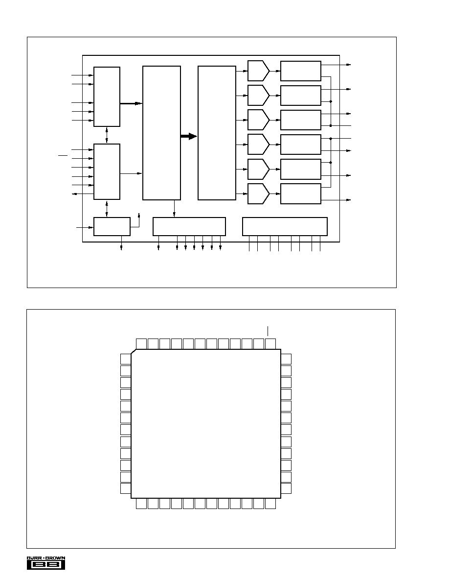
PIN CONFIGURATION
Top View
LQFP, MQFP
BLOCK DIAGRAM
36
35
34
33
32
31
30
29
28
27
26
25
ML
MC
MDI
MDO
NC
NC
V
CC
0
AGND0
V
CC
1
AGND1
V
CC
2
AGND2
ZEROA
DATA3
DATA2
DATA1
DGND
V
DD
TEST
LRCK
BCK
SCLKO
SCLKI
RST
V
OUT
2
V
OUT
1
V
COM
2
V
COM
1
AGND6
V
CC
6
AGND5
V
CC
5
AGND4
V
CC
4
AGND3
V
CC
3
1
2
3
4
5
6
7
8
9
10
11
12
ZERO1
ZERO2
ZERO3
ZERO4
ZERO5
ZERO6
AGND
V
CC
V
OUT
6
V
OUT
5
V
OUT
4
V
OUT
3
48
47
46
45
44
43
42
41
40
39
38
13
14
15
16
17
18
19
20
21
22
23
37
24
PCM1600
PCM1601
Audio
Serial
I/F
Output Amp and
Low-Pass Filter
DAC
DAC
DAC
DAC
DAC
DAC
8x
Oversampling
Digital Filter
with
Function
Controller
Enhanced
Multi-level
Delta-Sigma
Modulator
Output Amp and
Low-Pass Filter
Output Amp and
Low-Pass Filter
Output Amp and
Low-Pass Filter
Output Amp and
Low-Pass Filter
Output Amp and
Low-Pass Filter
BCK
LRCK
DATA1
DATA2
DATA3
Serial
Control
I/F
System Clock
Manager
Zero Detect
Power Supply
TEST
RST
ML
MC
MDI
MDO
V
OUT
1
V
OUT
2
V
OUT
5
V
OUT
6
V
OUT
3
V
COM
1
V
COM
2
V
OUT
4
ZERO1
ZERO2
ZERO3
ZERO4
ZERO5
ZERO6
V
DD
DGND
ZEROA
SCLKI
System Clock
SCLKO
V
CC
AGND
V
CC
0
AGND0
V
CC
1-6
AGND1-6
Æ
5
PCM1600, PCM1601
P I N
N A M E
I / O
DESCRIPTION
1
ZERO1
O
Zero Data Flag for V
OUT
1.
2
ZERO2
O
Zero Data Flag for V
OUT
2.
3
ZERO3
O
Zero Data Flag for V
OUT
3.
4
ZERO4
O
Zero Data Flag for V
OUT
4.
5
ZERO5
O
Zero Data Flag for V
OUT
5.
6
ZERO6
O
Zero Data Flag for V
OUT
6.
7
AGND
--
Analog Ground
8
V
CC
--
Analog Power Supply, +5V
9
V
OUT
6
O
Voltage Output of Audio Signal Corresponding to Rch on DATA3.
10
V
OUT
5
O
Voltage Output of Audio Signal Corresponding to Lch on DATA3.
11
V
OUT
4
O
Voltage Output of Audio Signal Corresponding to Rch on DATA2.
12
V
OUT
3
O
Voltage Output of Audio Signal Corresponding to Lch on DATA2.
13
V
OUT
2
O
Voltage Output of Audio Signal Corresponding to Rch on DATA1.
14
V
OUT
1
O
Voltage Output of Audio Signal Corresponding to Lch on DATA1.
15
V
COM
2
O
Common Voltage Output. This pin should be bypassed with a 10
µ
F capacitor to AGND.
16
V
COM
1
O
Common Voltage Output. This pin should be bypassed with a 10
µ
F capacitor to AGND.
17
AGND6
--
Analog Ground
18
V
CC
6
--
Analog Power Supply, +5V
19
AGND5
--
Analog Ground
20
V
CC
5
--
Analog Power Supply, +5V
21
AGND4
--
Analog Ground
22
V
CC
4
--
Analog Power Supply, +5V
23
AGND3
--
Analog Ground
24
V
CC
3
--
Analog Power Supply, +5V
25
AGND2
--
Analog Ground
26
V
CC
2
--
Analog Power Supply, +5V
27
AGND1
--
Analog Ground
28
V
CC
1
--
Analog Power Supply, +5V
29
AGND0
--
Analog Ground
30
V
CC
0
--
Analog Power Supply, +5V
31
NC
--
No Connection. Must be open.
32
NC
--
No Connection. Must be open.
33
MDO
O
Serial Data Output for Function Register Control Port
(3)
34
MDI
I
Serial Data Input for Function Register Control Port
(1)
35
MC
I
Shift Clock for Function Register Control Port
(1)
36
ML
I
Latch Enable for Function Register Control Port
(1)
37
RST
I
System Reset, Active LOW
(1)
38
SCLKI
I
System Clock In. Input frequency is 256, 384, 512 or 768f
S
.
(2)
39
SCLKO
O
Buffered Clock Output. Output frequency is 256, 384, 512, or 768f
S
and one-half of 256, 384, 512, or 768f
S.
40
BCK
I
Shift Clock Input for Serial Audio Data
(2)
41
LRCK
I
Left and Right Clock Input. This clock is equal to the sampling rate, f
S
.
(2)
42
TEST
--
Test Pin. This pin should be connected to DGND.
(1)
43
V
DD
--
Digital Power Supply, +3.3V
44
DGND
--
Digital Ground for +3.3V
45
DATA1
I
Serial Audio Data Input for V
OUT
1 and V
OUT
2
(2)
46
DATA2
I
Serial Audio Data Input for V
OUT
3 and V
OUT
4
(2)
47
DATA3
I
Serial Audio Data Input for V
OUT
5 and V
OUT
6
(2)
48
ZEROA
I
Zero Data Flag. Logical "AND" of ZERO1 through ZERO6.
NOTES: (1) Schmitt-Trigger input with internal pull-down, 5V tolerant. (2) Schmitt-Trigger input, 5V tolerant. (3) Tri-state output.
PIN ASSIGNMENTS
Æ
6
PCM1600, PCM1601
TYPICAL PERFORMANCE CURVES
All specifications at +25
∞
C, V
CC
= 5V, V
DD
= 3.3V, SYSCLK = 384f
S
(f
S
= 44.1kHz), and 24-bit input data, unless otherwise noted.
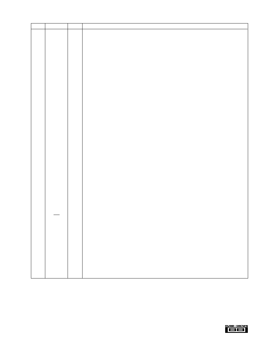
DIGITAL FILTER
Digital Filter (De-Emphasis Off, fS = 44.1kHz)
0
0.5
1
1.5
2
2.5
3
3.5
4
0
≠20
≠40
≠60
≠80
≠100
≠120
≠140
≠160
Amplitude (dB)
FREQUENCY RESPONSE
(Sharp Roll-Off)
Frequency (x f
S
)
PASSBAND RIPPLE
(Sharp Roll-Off)
Frequency (x f
S
)
Amplitude (dB)
0.003
0.002
0.001
0
≠0.001
≠0.002
≠0.003
0
0.1
0.2
0.3
0.4
0.5
FREQUENCY RESPONSE
(Slow Roll-Off)
Frequency (x f
S
)
Amplitude (dB)
0
≠20
≠40
≠60
≠80
≠100
≠120
≠140
0
0.5
1.0
1.5
2.0
2.5
3.0
3.5
4.0
TRANSITION CHARACTERISTICS
(Slow Roll-Off)
Frequency (x f
S
)
Amplitude (dB)
0
≠2
≠4
≠6
≠8
≠10
≠12
≠14
≠16
≠18
≠20
0
0.1
0.2
0.3
0.4
0.5
0.6
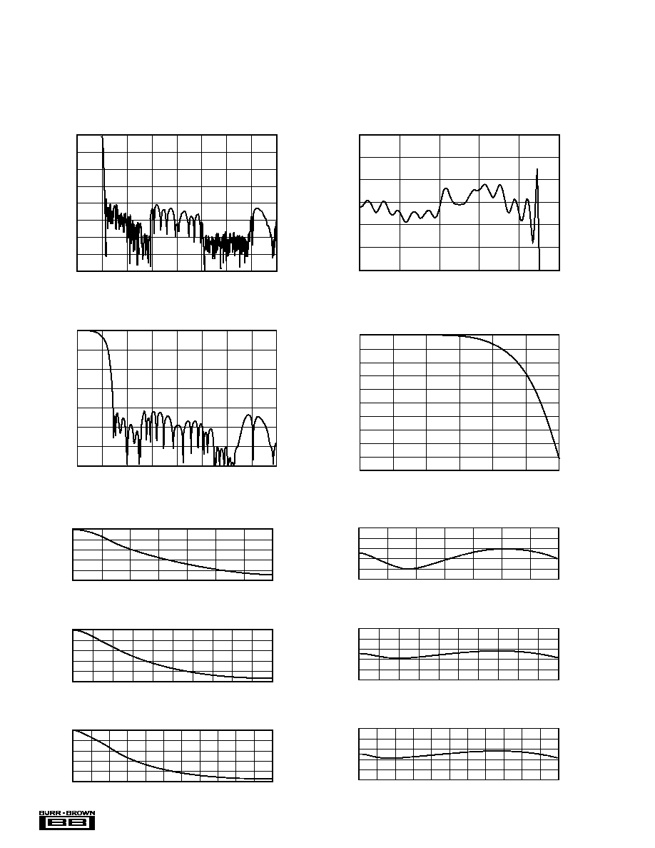
DE-EMPHASIS FREQUENCY RESPONSE (f
S
= 32kHz)
0
2
4
6
8
10
12
14
Frequency (kHz)
0
≠2
≠4
≠6
≠8
≠10
Level (dB)
DE-EMPHASIS FREQUENCY RESPONSE (f
S
= 48kHz)
0
2
4
6
8
10
12
14
16
18
20
22
Frequency (kHz)
0
≠2
≠4
≠6
≠8
≠10
Level (dB)
DE-EMPHASIS FREQUENCY RESPONSE (f
S
= 44.1kHz)
0
2
4
6
8
10
12
14
16
18
20
Frequency (kHz)
0
≠2
≠4
≠6
≠8
≠10
Level (dB)
DE-EMPHASIS ERROR (f
S
= 32kHz)
0
2
4
6
8
10
12
14
Frequency (kHz)
0.5
0.3
0.1
≠0.1
≠0.3
≠0.5
0.5
0.3
0.1
≠0.1
≠0.3
≠0.5
0.5
0.3
0.1
≠0.1
≠0.3
≠0.5
Level (dB)
DE-EMPHASIS ERR0R (f
S
= 48kHz)
0
2
4
6
8
10
12
14
16
18
20
22
Frequency (kHz)
Level (dB)
DE-EMPHASIS ERROR (f
S
= 44.1kHz)
0
2
4
6
8
10
12
14
16
18
20
Frequency (kHz)
Level (dB)
De-Emphasis Error
Æ
7
PCM1600, PCM1601
TYPICAL PERFORMANCE CURVES
(Cont.)
All specifications at +25
∞
C, V
CC
= 5V, V
DD
= 3.3V, SYSCLK = 384f
S
(f
S
= 44.1kHz), and 24-bit input data, unless otherwise noted.
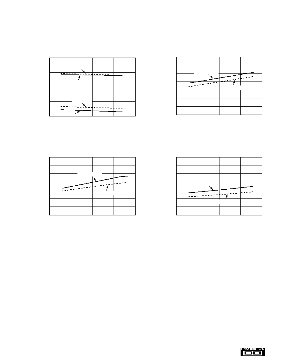
ANALOG DYNAMIC PERFORMANCE
Supply Voltage Characteristics
TOTAL HARMONIC DISTORTION + NOISE vs V
CC
(V
DD
= 3.3V)
V
CC
(V)
THD+N (%)
10
1
0.1
0.01
0.001
4.0
4.5
5.0
5.5
6.0
44.1kHz, 384f
S
44.1kHz, 384f
S
96kHz, 384f
S
≠60dB
0dB
96kHz, 384f
S
DYNAMIC RANGE vs V
CC
(V
DD
= 3.3V)
V
CC
(V)
Dynamic Range (dB)
110
108
106
104
102
100
98
96
4.0
4.5
5.0
5.5
6.0
96kHz, 384f
S
44.1kHz, 384f
S
SIGNAL-TO-NOISE RATIO vs V
CC
(V
DD
= 3.3V)
V
CC
(V)
SNR (dB)
110
108
106
104
102
100
98
96
4.0
4.5
5.0
5.5
6.0
96kHz, 384f
S
44.1kHz, 384f
S
CHANNEL SEPARATION vs V
CC
(V
DD
= 3.3V)
V
CC
(V)
Channel Separation (dB)
110
108
106
104
102
100
98
96
4.0
4.5
5.0
5.5
6.0
96kHz, 384f
S
44.1kHz, 384f
S
Æ
8
PCM1600, PCM1601
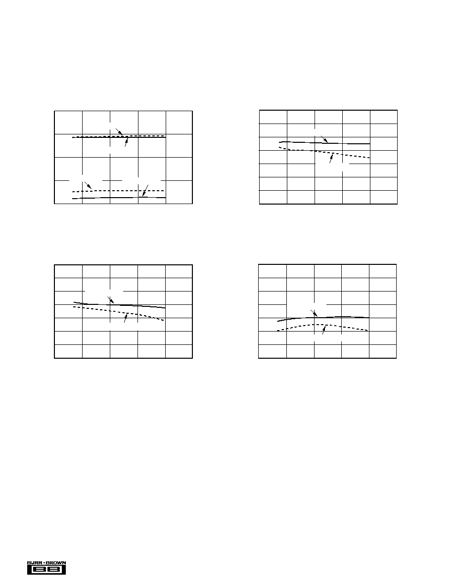
TOTAL HARMONIC DISTORTION + NOISE
vs TEMPERATURE
(V
DD
= 3.3V)
Temperature (
∞
C)
THD+N (%)
10
1
0.1
0.01
0.001
≠25
0
25
50
75
100
44.1kHz, 384f
S
44.1kHz, 384f
S
96kHz, 384f
S
≠60dB
0dB
96kHz, 384f
S
DYNAMIC RANGE vs TEMPERATURE
(V
DD
= 3.3V)
Temperature (
∞
C)
Dynamic Range (dB)
110
108
106
104
102
100
98
96
≠25
0
25
50
75
100
96kHz, 384f
S
44.1kHz, 384f
S
TYPICAL PERFORMANCE CURVES
(Cont.)
All specifications at +25
∞
C, V
CC
= 5V, V
DD
= 3.3V, SYSCLK = 384f
S
(f
S
= 44.1kHz), and 24-bit input data, unless otherwise noted.
ANALOG DYNAMIC PERFORMANCE (con.t)
Temperature Characteristics
SIGNAL-TO-NOISE RATIO vs TEMPERATURE
(V
DD
= 3.3V)
Temperature (
∞
C)
SNR (dB)
110
108
106
104
102
100
98
96
≠25
0
25
50
100
75
96kHz, 384f
S
44.1kHz, 384f
S
CHANNEL SEPARATION vs TEMPERATURE
(V
DD
= 3.3V)
Temperature (
∞
C)
Channel Separation (dB)
110
108
106
104
102
100
98
96
≠25
0
25
50
75
100
96kHz, 384f
S
44.1kHz, 384f
S
Æ
9
PCM1600, PCM1601
FIGURE 1. System Clock Input Timing.
SYSTEM CLOCK AND RESET
FUNCTIONS
SYSTEM CLOCK INPUT
The PCM1600 and PCM1601 require a system clock for
operating the digital interpolation filters and multi-level
delta-sigma modulators. The system clock is applied at the
SCLKI input (pin 38). For sampling rates from 10kHz
through 64kHz, the system clock frequency may be 256,
384, 512, or 768 times the sampling frequency, f
S
. For
sampling rates above 64kHz, the system clock frequency
may be 256, 384, or 512 times the sampling frequency.
Table I shows examples of system clock frequencies for
common audio sampling rates.
Figure 1 shows the timing requirements for the system clock
input. For optimal performance, it is important to use a clock
source with low phase jitter and noise. Burr-Brown's
PLL1700 multi-clock generator is an excellent choice for
providing the PCM1600 system clock source.
SYSTEM CLOCK OUTPUT
A buffered version of the system clock input is available at
the SCLKO output (pin 39). SCLKO can operate at either
full (f
SCLKI
) or half (f
SCLKI
/2) rate. The SCLKO output
frequency may be programmed using the CLKD bit of
Control Register 9. The SCLKO output pin can also be
enabled or disabled using the CLKE bit of Control Register
9. The default is SCLKO enabled.
POWER-ON AND EXTERNAL RESET FUNCTIONS
The PCM1600 includes a power-on reset function. Figure 2
shows the operation of this function.
The system clock input at SCLKI should be active for at
least one clock period prior to V
DD
= 2.0V. With the system
clock active and V
DD
> 2.0V, the power-on reset function
will be enabled. The initialization sequence requires 1024
system clocks from the time V
DD
> 2.0V. After the initial-
ization period, the PCM1600 will be set to its reset default
state, as described in the Mode Control Register section of
this data sheet.
The PCM1600 also includes an external reset capability
using the RST input (pin 37). This allows an external
controller or master reset circuit to force the PCM1600 to
initialize to its reset default state. For normal operation, RST
should be set to a logic `1'.
Figure 3 shows the external reset operation and timing. The
RST pin is set to logic `0' for a minimum of 20ns. The RST
pin is then set to a logic `1' state, which starts the initializa-
tion sequence, which lasts for 1024 system clock periods.
After the initialization sequence is completed, the PCM1600
will be set to its reset default state, as described in the Mode
Control Registers section of this data sheet.
t
SCLKIH
t
SCLKIH
f
SCLKI
System Clock Pulse Width High t
SCLKIH
: 7ns min
System Clock Pulse Width Low t
SCLKIL
: 7ns min
2.0V
0.8V
"H"
"L"
SCLKI
SAMPLING
FREQUENCY (f
S
)
256f
S
384f
S
512f
S
768f
S
22.05kHz
5.6448
8.4670
11.2896
16.9340
24kHz
6.1440
9.2160
12.2880
18.4320
32kHz
8.1920
12.2880
16.3840
24.5760
44.1kHz
11.2896
16.9340
22.5792
33.8688
48kHz
12.2880
18.4320
24.5760
36.8640
64kHz
16.3840
24.5760
32.7680
49.1520
88.2kHz
22.5792
33.8688
45.1584
See Note 1
96kHz
24.5760
36.8640
49.1520
See Note 1
NOTE: (1) The 768f
S
system clock rate is not supported for f
S
> 64kHz.
TABLE I. System Clock Rates for Common Audio Sampling
Frequencies.
SYSTEM CLOCK FREQUENCY (MHz)
SCLKI (Pin 38)
Æ
10
PCM1600, PCM1601
FIGURE 2. Power-On Reset Timing.
FIGURE 3. External Reset Timing.
The external reset is especially useful in applications
where there is a delay between PCM1600 power up and
system clock activation. In this case, the RST pin should
be held at a logic `0' level until the system clock has been
activated.
AUDIO SERIAL INTERFACE
The audio serial interface for the PCM1600 is comprised
of a 5-wire synchronous serial port. It includes LRCK (pin
41), BCK (pin 40), DATA1 (pin 45), DATA2 (pin 46) and
DATA3 (pin 47). BCK is the serial audio bit clock, and is
used to clock the serial data present on DATA1, DATA2
and DATA3 into the audio interface's serial shift registers.
Serial data is clocked into the PCM1600 on the rising edge
of BCK. LRCK is the serial audio left/right word clock. It
is used to latch serial data into the serial audio interface's
internal registers.
Both LRCK and BCK must be synchronous to the system
clock. Ideally, it is recommended that LRCK and BCK be
derived from the system clock input or output, SCLKI or
SCLKO. The left/right clock, LRCK, is operated at the
sampling frequency (f
S
). The bit clock, BCK, may be
operated at 48 or 64 times the sampling frequency.
AUDIO DATA FORMATS AND TIMING
The PCM1600 supports industry-standard audio data for-
mats, including Standard, I
2
S, and Left-Justified. The data
formats are shown in Figure 4. Data formats are selected
using the format bits, FMT[2:0], in Control Register 9. The
default data format is 24-bit Standard. All formats require
Binary Two's Complement, MSB-first audio data. Figure 5
shows a detailed timing diagram for the serial audio interface.
DATA1, DATA2 and DATA3 each carry two audio channels,
designated as the Left and Right channels. The Left channel
data always precedes the Right channel data in the serial data
stream for all data formats. Table II shows the mapping of the
digital input data to the analog output pins.
DATA INPUT
CHANNEL
ANALOG OUTPUT
DATA1
Left
V
OUT
1
DATA1
Right
V
OUT
2
DATA2
Left
V
OUT
3
DATA2
Right
V
OUT
4
DATA3
Left
V
OUT
5
DATA3
Right
V
OUT
6
TABLE II. Audio Input Data to Analog Output Mapping.
1024 system clocks
Reset
Reset Removal
V
CC
= V
DD
Internal Reset
2.4V
2.0V
1.6V
System Clock
(SCLKI)
1024 system clocks
Reset
Reset Removal
System Clock
(SCLKI)
Internal Reset
RST
t
RST
(1)
NOTE: (1) t
RST
= 20ns min.
SERIAL CONTROL INTERFACE
The serial control interface is a 4-wire synchronous serial port
which operates asynchronously to the serial audio interface.
The serial control interface is utilized to program and read the
on-chip mode registers. The control interface includes MDO
(pin 33), MDI (pin 34), MC (pin 35), and ML (pin 36). MDO
is the serial data output, used to read back the values of the
mode registers; MDI is the serial data input, used to program
the mode registers; MC is the serial bit clock, used to shift
data in and out of the control port and ML is the control port
latch clock.
Æ
11
PCM1600, PCM1601
FIGURE 4. Audio Data Input Formats.
1/f
S
Lch
Rch
LRCK
BCK
(= 48f
S
or 64f
S
)
16-Bit Right-Justified
18-Bit Right-Justified
DATA1-DATA3
DATA1-DATA3
(2) 24-Bit Left-Justified Data Format; Lch = HIGH, Rch = LOW
(3) 24-Bit I
2
S Data Format; Lch = LOW, Rch = HIGH
(1) Standard Data Format; Lch = HIGH, Rch = LOW
1/f
S
Lch
Rch
LRCK
BCK
(= 48f
S
or 64f
S
)
1
2
3
22
23
24
1
2
3
22
23
24
1/f
S
Lch
Rch
LRCK
BCK
(= 48f
S
or 64f
S
)
2
1
1
2
3
22
23
24
1
2
3
22
23
24
14
15
16
16
17
18
18
19
20
14
15
16
12
3
DATA1-DATA3
22
23
24
22
23
24
12
3
45
DATA1-DATA3
18
19
20
1
23
DATA1-DATA3
16
17
18
1
23
DATA1-DATA3
24-Bit Right-Justified
14
15
16
12
3
22
23
24
12
3
45
18
19
20
1
23
16
17
18
1
23
20-Bit Right-Justified
LSB
MSB
LSB
MSB
LSB
MSB
LSB
MSB
LSB
MSB
LSB
MSB
LSB
MSB
LSB
MSB
LSB
MSB
LSB
MSB
LSB
MSB
Æ
12
PCM1600, PCM1601
REGISTER WRITE OPERATION
All Write operations for the serial control port use 16-bit
data words. Figure 6 shows the control data word format.
The most significant bit is the Read/Write (R/W) bit. When
set to `0', this bit indicates a Write operation. There are
seven bits, labeled IDX[6:0], that set the register index (or
address) for the Write operation. The least significant eight
bits, D[7:0], contain the data to be written to the register
specified by IDX[6:0].
Figure 7 shows the functional timing diagram for writing the
serial control port. ML is held at a logic `1' state until a
register needs to be written. To start the register write cycle,
ML is set to logic `0'. Sixteen clocks are then provided on
MC, corresponding to the 16-bits of the control data word on
MDI. After the sixteenth clock cycle has completed, ML is
set to logic `1' to latch the data into the indexed mode
control register.
IDX5
IDX6
R/W
IDX4
IDX2
IDX3
IDX1
IDX0
D7
D6
D5
D4
D3
D2
D5
D4
D3
D2
D1
D0
MSB
Register Index (or Address)
Read/Write Operation
0 = Write Operation
1 = Read Operation (register index is ignored)
Register Data
LSB
FIGURE 6. Control Data Word Format for MDI.
FIGURE 7. Write Operation Timing.
SINGLE REGISTER READ OPERATION
Read operations utilize the 16-bit control word format shown
in Figure 6. For Read operations, the Read/Write (R/W) bit
is set to `1'. Read operations ignore the index bits, IDX[6:0],
of the control data word. Instead, the REG[6:0] bits in
Control Register 11 are used to set the index of the register
that is to be read during the Read operation. Bits IDX[6:0]
should be set to 00
H
for Read operations.
Figure 8 details the Read operation. First, Control Register
11 must be written with the index of the register to be read
back. Additionally, the INC bit must be set to logic `0' in
order to disable the Auto-Increment Read function. The
Read cycle is then initiated by setting ML to logic `0' and
setting the R/W bit of the control data word to logic `1',
indicating a Read operation. MDO remains at a high-imped-
ance state until the last 8 bits of the 16-bit read cycle, which
0
D7
D6
D5
D4
D3
D2
D15 D14
D1
D0
X
X
X
IDX6 IDX5 IDX4 IDX3 IDX2 IDX1 IDX0
ML
MC
MDI
FIGURE 5. Audio Interface Timing.
SYMBOL
PARAMETER
MIN
MAX
UNITS
t
BCY
BCK Pulse Cycle Time
48 or 64f
S
(1)
t
BCH
BCK High Level Time
50
ns
t
BCL
BCK Low Level Time
50
ns
t
BL
BCK Rising Edge to LRCK Edge
30
ns
t
LB
LRCK Falling Edge to BCK Rising Edge
30
ns
t
DS
DIN Set Up Time
30
ns
t
DH
DIN Hold Time
20
ns
NOTE: (1) f
S
is the sampling frequency (e.g., 44.1kHz, 48kHz, 96kHz, etc.)
LRCK
BCK
DATA1-DATA3
50% of V
DD
50% of V
DD
50% of V
DD
t
BCH
t
BCL
t
LB
t
BL
t
DS
t
DH
t
BCY
Æ
13
PCM1600, PCM1601
FIGURE 8. Read Operation Timing with INC = 0 (Single Register Read).
FIGURE 9. Read Operation Timing with INC = 1 (Auto-Increment Read).
0
00
01
01
10
X
X
X
X
X
X
X
X
X
X
10
0
0
0
0
0
0
REG6
REG5
REG4
REG3
REG2
REG1
REG0
ML
I
O
I
O
I
O
I
O
High Impedance
Read Register Index
Write
MC
MDI
MDO
D7
D6
D5
D4
D3
D2
D1
D0
Read
Writing Register 11 with INC and REG[6:0] Data
X = Don't care
Register Read Cycle
Data from Register Indexed by REG[6:0]
10
00
00
00
X
X
XX
XXXX
X
X
X
X
X
X
X
X
X
XX
X
XX
X
X
X
High Impedance
ML
MC
MDI
MDO
D7
D0
D6
D5
D4
D3
D2
D1
D0
High Impedance
D7
D6
D5
D4
INDEX "N ≠ 1"
D3
D2
D1
D6
D7
D5
D4
D3
D2
D1
D0
INDEX "1"
INDEX "N"
Æ
14
PCM1600, PCM1601
corresponds to the 8 data bits of the register indexed by the
REG[6:0] bits of Control Register 11. The Read cycle is
completed when ML is set to `1', immediately after the MC
clock cycle for the least significant bit of indexed control
register has completed.
AUTO-INCREMENT READ OPERATION
The Auto-Increment Read function allows for multiple reg-
isters to be read sequentially. The Auto-Increment Read
function is enabled by setting the INC bit of Control Register
11 to `1'. The sequence always starts with Register 1, and
ends with the register indexed by the REG[6:0] bits in
Control Register 11.
Figure 9 shows the timing for the Auto-Increment Read
operation. The operation begins by writing Control Register
11, setting INC to `1' and setting REG[6:0] to the last
register to be read in the sequence. The actual Read opera-
tion starts on the next HIGH to LOW transition of the ML
50% of V
DD
50% of V
DD
50% of V
DD
50% of V
DD
ML
MC
MDI
MDO
t
MLS
t
MCH
t
MCY
t
MOS
t
MDS
t
MCH
t
MCL
t
MHH
t
MLH
LSB
LSB
pin. The Read cycle starts by setting the R/W bit of the
control word to `1', and setting all of the IDX[6:0] bits to
`0.'. All subsequent bits input on the MDI are ignored while
ML is set to `0.' For the first 8 clocks of the Read cycle,
MDO is set to a high-impedance state. This is followed by
a sequence of 8-bit words, each corresponding the data
contained in Control Registers 1 through N, where N is
defined by the REG[6:0] bits in Control Register 11. The
Read cycle is completed when ML is set to `1', immediately
after the MC clock cycle for the least significant bit of
Control Register N has completed.
CONTROL INTERFACE TIMING REQUIREMENTS
Figure 10 shows a detailed timing diagram for the Serial
Control interface. Pay special attention to the setup and hold
times, as well as t
MLS
and t
MLH
, which define minimum delays
between edges of the ML and MC clocks. These timing
parameters are critical for proper control port operation.
SYMBOL
PARAMETER
MIN
MAX
UNITS
t
MCY
MC Pulse Cycle Time
100
ns
t
MCL
MC Low Level Time
50
ns
t
MCH
MC High Level Time
50
ns
t
MHH
ML High Level Time
300
ns
t
MLS
ML Falling Edge to MC Rising Edge
20
ns
t
MLH
ML Hold Time
(1)
20
ns
t
MDI
Hold Time
15
ns
t
MDS
MDL Set Up Time
20
ns
t
MOS
MC Falling Edge to MDSO Stable
30
ns
NOTE: (1) MC rising edge for LSB to ML rising edge.
FIGURE 10. Control Interface Timing.
Æ
15
PCM1600, PCM1601
MODE CONTROL REGISTERS
User-Programmable Mode Controls
The PCM1600 includes a number of user-programmable
functions which are accessed via control registers. The
registers are programmed using the Serial Control Interface
which was previously discussed in this data sheet. Table III
lists the available mode control functions, along with their
reset default conditions and associated register index.
FUNCTION
RESET DEFAULT
CONTROL REGISTER
INDEX, IDX[6:0]
Digital Attenuation Control, 0dB to ≠63dB in 0.5dB Steps
0dB, No Attenuation
1 through 6
01
H
- 07
H
Digital Attenuation Load Control
Data Load Disabled
7
07
H
Digital Attenuation Rate Select
2/f
S
7
07
H
Soft Mute Control
Mute Disabled
7
07
H
DAC 1-6 Operation Control
DAC 1-6 Enabled
8
08
H
Infinite Zero Detect Mute
Disabled
8
08
H
Audio Data Format Control
24-Bit Standard Format
9
09
H
Digital Filter Roll-Off Control
Sharp Roll-Off
9
09
H
SCLKO Frequency Selection
Full Rate (= f
SCLKI
)
9
09
H
SCLKO Output Enable
SCLKO Enabled
9
09
H
De-Emphasis Function Control
De-Emphasis Disabled
10
0A
H
De-Emphasis Sample Rate Selection
44.1kHz
10
0A
H
Read Register Index Control
REG[6:0] = 01
H
11
0B
H
Read Auto-Increment Control
Auto-Increment Disabled
11
0B
H
TABLE III. User-Programmable Mode Controls.
TABLE IV. Mode Control Register Map.
B15
B14
B13
B12
B11
B10
B9
B8
B7
B6
B5
B4
B3
B2
B1
B0
Register 0
R/W
IDX6
IDX5
IDX4
IDX3
IDX2
IDX1
IDX0
N/A
N/A
N/A
N/A
N/A
N/A
N/A
N/A
Register 1
R/W
IDX6
IDX5
IDX4
IDX3
IDX2
IDX1
IDX0
AT17
AT16
AT15
AT14
AT13
AT12
AT11
AT10
Register 2
R/W
IDX6
IDX5
IDX4
IDX3
IDX2
IDX1
IDX0
AT27
AT26
AT25
AT24
AT23
AT22
AT21
AT20
Register 3
R/W
IDX6
IDX5
IDX4
IDX3
IDX2
IDX1
IDX0
AT37
AT36
AT35
AT34
AT33
AT32
AT31
AT30
Register 4
R/W
IDX6
IDX5
IDX4
IDX3
IDX2
IDX1
IDX0
AT47
AT46
AT45
AT44
AT43
AT42
AT41
AT40
Register 5
R/W
IDX6
IDX5
IDX4
IDX3
IDX2
IDX1
IDX0
AT57
AT56
AT55
AT54
AT53
AT52
AT51
AT50
Register 6
R/W
IDX6
IDX5
IDX4
IDX3
IDX2
IDX1
IDX0
AT67
AT66
AT65
AT64
AT63
AT62
AT61
AT60
Register 7
R/W
IDX6
IDX5
IDX4
IDX3
IDX2
IDX1
IDX0
ATLD
ATTS
MUT6
MUT5
MUT4
MUT3
MUT2 MUT1
Register 8
R/W
IDX6
IDX5
IDX4
IDX3
IDX2
IDX1
IDX0
res
INZD
DAC6
DAC5
DAC4
DAC3
DAC2 DAC1
Register 9
R/W
IDX6
IDX5
IDX4
IDX3
IDX2
IDX1
IDX0
res
res
FLT0
CLKD
CLKE
FMT2
FMT1
FMT0
Register 10
R/W
IDX6
IDX5
IDX4
IDX3
IDX2
IDX1
IDX0
res
res
res
DMF1
DMF0
DM56
DM34 DM12
Register 11
R/W
IDX6
IDX5
IDX4
IDX3
IDX2
IDX1
IDX0
INC
REG6
REG5
REG4
REG3
REG2
REG1 REG0
Register 12
R/W
IDX6
IDX5
IDX4
IDX3
IDX2
IDX1
IDX0
N/A
N/A
N/A
N/A
N/A
N/A
N/A
N/A
Register Map
The mode control register map is shown in Table IV. Each
register includes a R/W bit, which determines whether a
register read (R/W =1) or write (R/W = 0) operation is
performed. Each register also includes an index (or address)
indicated by the IDX[6:0] bits.
Reserved Registers
Registers 0 and 12 are reserved for factory use. To ensure
proper operation, the user should not write or read these
registers.
Æ
16
PCM1600, PCM1601
B15
B14
B13
B12
B11
B10
B9
B8
B7
B6
B5
B4
B3
B2
B1
B0
Register 1
R/W
IDX6
IDX5
IDX4
IDX3
IDX2
IDX1
IDX0
AT17
AT16
AT15
AT14
AT13
AT12
AT11
AT10
Register 2
R/W
IDX6
IDX5
IDX4
IDX3
IDX2
IDX1
IDX0
AT27
AT26
AT25
AT24
AT23
AT22
AT21
AT20
Register 3
R/W
IDX6
IDX5
IDX4
IDX3
IDX2
IDX1
IDX0
AT37
AT36
AT35
AT34
AT33
AT32
AT31
AT30
Register 4
R/W
IDX6
IDX5
IDX4
IDX3
IDX2
IDX1
IDX0
AT47
AT46
AT45
AT44
AT43
AT42
AT41
AT40
Register 5
R/W
IDX6
IDX5
IDX4
IDX3
IDX2
IDX1
IDX0
AT57
AT56
AT55
AT54
AT53
AT52
AT51
AT50
Register 6
R/W
IDX6
IDX5
IDX4
IDX3
IDX2
IDX1
IDX0
AT67
AT66
AT65
AT64
AT63
AT62
AT61
AT60
REGISTER DEFINITIONS
R/W
Read/Write Mode Select
When R/W = 0, a Write operation is performed.
When R/W = 1, a Read operation is performed.
Default Value: 0
ATx[7:0]
Digital Attenuation Level Setting
where x = 1-6, corresponding to the DAC output V
OUT
x.
These bits are Read/Write.
Default Value: 1111 1111
B
Each DAC output, V
OUT
1 through V
OUT
6, has a digital attenuator associated with it. The attenuator may be
set from 0dB to ≠63dB, in 0.5dB steps. Alternatively, the attenuator may be set to infinite attenuation (or
mute).
The attenuation data for each channel can be set individually. However, the data load control (ATLD bit of
Control Register 7) is common to all six attenuators. ATLD must be set to `1' in order to change an
attenuator's setting. The attenuation level may be set using the formula below.
Attenuation Level (dB) = 0.5 (AT x [7:0]
DEC
≠ 255)
where: AT x [7:0]
DEC
= 0 through 255
for: AT x [7:0]
DEC
= 0 through 128, the attenuator is set to infinite attenuation.
The following table shows attenuator levels for various settings.
ATx[7:0]
Decimal Value
Attenuator Level Setting
1111 1111
B
255
0dB, No Attenuation (default)
1111 1110
B
254
≠0.5dB
1111 1101
B
253
≠1.0dB
∑
∑
∑
∑
∑
∑
∑
∑
∑
1000 0010
B
130
≠62.5dB
1000 0001
B
129
≠63.0dB
1000 0000
B
128
Mute
∑
∑
∑
∑
∑
∑
∑
∑
∑
0000 0000
B
0
Mute
Æ
17
PCM1600, PCM1601
B15
B14
B13
B12
B11
B10
B9
B8
B7
B6
B5
B4
B3
B2
B1
B0
Register 7
R/W
IDX6
IDX5
IDX4
IDX3
IDX2
IDX1
IDX0
ATLD
ATTS
MUT6
MUT5
MUT4
MUT3
MUT2
MUT1
R/W
Read/Write Mode Select
When R/W = 0, a Write operation is performed.
When R/W = 1, a Read operation is performed.
Default Value: 0
ATLD
Attenuation Control
This bit is Read/Write.
Default Value: 0
ATLD = 0
Attenuation Control Disabled (default)
ATLD = 1
Attenuation Control Enabled
The ATLD bit must be set to logic "1" in order for the attenuators to function. Setting ATLD to logic "0" will
disable the attenuator function and cause the current attenuator data to be lost.
Set ATLD = 1 immediately after reset.
ATTS
Attenuation Rate Select
This bit is Read/Write.
Default Value: 0
ATTS = 0
Attenuation rate is 2/f
S
(default)
ATTS = 1
Attenuation rate is 4/f
S
Changes in attenuator levels are made by incrementing or decrementing the attenuator by one step (0.5dB) for
every 2/f
S
or 4/f
S
time interval until the programmed attenuator setting is reached. This helps to minimize
audible `clicking', or zipper noise, while the attenuator is changing levels. The ATTS bit allows you to select
the rate at which the attenuator is decremented/incremented during level transitions.
MUTx
Soft Mute Control
where x = 1-6, corresponding to the DAC output V
OUT
x.
These bits are Read/Write.
Default Value: 0
MUTx = 0
Mute Disabled (default)
MUTx = 1
Mute Enabled
The mute bits, MUT1 through MUT6, are used to enable or disable the Soft Mute function for the
corresponding DAC outputs, V
OUT
1 through V
OUT
6. The Soft Mute function is incorporated into the digital
attenuators. When Mute is disabled (MUTx = 0), the attenuator and DAC operate normally. When Mute
is enabled by setting MUTx = 1, the digital attenuator for the corresponding output will be decremented
from the current setting to the infinite attenuation setting one attenuator step (0.5dB) at a time, with the rate
of change programmed by the ATTS bit. This provides a quiet, `pop' free muting of the DAC output. Upon
returning from Soft Mute, by setting MUTx = 0, the attenuator will be incremented one step at a time to
the previously programmed attenuator level.
Æ
18
PCM1600, PCM1601
R/W
Read/Write Mode Select
When R/W = 0, a Write operation is performed.
When R/W = 1, a Read operation is performed.
Default Value: 0
INZD
Infinite Zero Detect Mute Control
This bit is Read/Write.
Default Value: 0
INZD = 0
Infinite Zero Detect Mute Disabled (default)
INZD = 1
Infinite Zero Detect Mute Enabled
The INZD bit is used to enable or disable the Zero Detect Mute function described in the Zero Flag and Infinite
Zero Detect Mute section in this data sheet. The Zero Detect Mute function is independent of the Zero Flag
output operation, so enabling or disabling the INZD bit has no effect on the Zero Flag outputs (ZERO1-ZERO6,
ZEROA).
DACx
DAC Operation Control
where x = 1-6, corresponding to the DAC output V
OUT
x.
These bits are Read/Write.
Default Value: 0
DACx = 0
DAC Operation Enabled (default)
DACx = 1
DAC Operation Disabled
The DAC operation controls are used to enable and disable the DAC outputs, V
OUT
1 through V
OUT
6. When
DACx = 0, the output amplifier input is connected to the DAC output. When DACx = 1, the output amplifier
input is switched to the DC common-mode voltage (V
COM
1 or V
COM
2), equal to V
CC
/2.
B15
B14
B13
B12
B11
B10
B9
B8
B7
B6
B5
B4
B3
B2
B1
B0
REGISTER 8
R/W
IDX6
IDX5
IDX4
IDX3
IDX2
IDX1
IDX0
res
INZD
DAC6
DAC5
DAC4
DAC3
DAC2
DAC1
Æ
19
PCM1600, PCM1601
B15
B14
B13
B12
B11
B10
B9
B8
B7
B6
B5
B4
B3
B2
B1
B0
REGISTER 9
R/W
IDX6
IDX5
IDX4
IDX3
IDX2
IDX1
IDX0
res
res
FLT0
CLKD
CLKE
FMT2
FMT1
FMT0
R/W
Read/Write Mode Select
When R/W = 0, a Write operation is performed.
When R/W = 1, a Read operation is performed.
Default Value: 0
FLT0
Digital Filter Roll-Off Control
These bits are Read/Write.
Default Value: 000
B
FLT0 = 0
Sharp Roll-Off (default)
FLT0 = 1
Slow Roll-Off
Bit FLT0 allows the user to select the digital filter roll-off that is best suited to their application. Two filter roll-
off sections are available: Sharp or Slow. The filter responses for these selections are shown in the Typical
Performance Curves section of this data sheet.
CLKD
SCLKO Frequency Selection
This bit is Read/Write.
Default Value: 0
CLKD = 0
Full Rate, f
SCLKO
= f
SCLKI
(default)
CLKD = 1
Half Rate, f
SCLKO
= f
SCLKL
/2
The CLKD bit is used to determine the clock frequency at the system clock output pin, SCLKO.
CLKE
SCLKO Output Enable
This bit is Read/Write.
Default Value: 0
CLKE = 0
SCLKO Enabled (default)
CLKE = 1
SCLKO Disabled
The CLKE bit is used to enable or disable the system clock output pin, SCLKO. When SCLKO is enabled, it
will output either a full or half rate clock, based upon the setting of the CLKD bit. When SCLKO is disabled,
it is set to a high impedance state.
FMT[2:0]
Audio Interface Data Format
These bits are Read/Write.
Default Value: 000
B
FMT[2:0]
Audio Data Format Selection
000
24-Bit Standard Format, Right-Justified Data (default)
001
20-Bit Standard Format, Right-Justified Data
010
18-Bit Standard Format, Right-Justified Data
011
16-Bit Standard Format, Right-Justified Data
100
I
2
S Format, 16- to 24-bits
101
Left-Justified Format, 16- to 24-Bits
110
Reserved
111
Reserved
The FMT[2:0] bits are used to select the data format for the serial audio interface.
Æ
20
PCM1600, PCM1601
B15
B14
B13
B12
B11
B10
B9
B8
B7
B6
B5
B4
B3
B2
B1
B0
REGISTER 10
R/W
IDX6
IDX5
IDX4
IDX3
IDX2
IDX1
IDX0
res
res
res
DMF1
DMF0
DM56
DM34
DM12
R/W
Read/Write Mode Select
When R/W = 0, a Write operation is performed.
When R/W = 1, a Read operation is performed.
Default Value: 0
DMF[1:0]
Sampling Frequency Selection for the De-Emphasis Function
These bits are Read/Write.
Default Value: 00
B
DMF[1:0]
De-Emphasis Same Rate Selection
00
44.1 kHz (default)
01
48 kHz
10
32 kHz
11
Reserved
The DMF[1:0] bits are used to select the sampling frequency used for the Digital De-Emphasis function when
it is enabled. The de-emphasis curves are shown in the Typical Performance Curves section of this data sheet.
The table below shows the available sampling frequencies.
DM12
Digital De-Emphasis Control for Channels 1 and 2
This bit is Read/Write.
Default Value: 0
DM12 = 0
De-Emphasis Disabled for Channels 1 and 2 (default)
DM12 = 1
De-Emphasis Enabled for Channels 1 and 2
The DM12 bit is used to enable or disable the De-emphasis function for V
OUT
1 and V
OUT
2, which correspond
to the Left and Right channels of the DATA1 input.
DM34
Digital De-Emphasis Control for Channels 3 and 4
This bit is Read/Write.
Default Value: 0
DM34 = 0
De-Emphasis Disabled for Channels 3 and 4 (default)
DM34 = 1
De-Emphasis Enabled for Channels 3 and 4
The DM34 bit is used to enable or disable the De-Emphasis function for V
OUT
3 and V
OUT
4, which correspond
to the Left and Right channels of the DATA2 input.
DM56
Digital De-Emphasis Control for Channels 5 and 6
This bit is Read/Write.
Default Value: 0
DM56 = 0
De-Emphasis Disabled for Channels 5 and 6 (default)
DM56 = 1
De-Emphasis Enabled for Channels 5 and 6
The DM56 bit is used to enable or disable the de-emphasis function for V
OUT
5 and V
OUT
6, which correspond
to the Left and Right channels of the DATA3 input.

Æ
21
PCM1600, PCM1601
B15
B14
B13
B12
B11
B10
B9
B8
B7
B6
B5
B4
B3
B2
B1
B0
REGISTER 11
R/W
IDX6
IDX5
IDX4
IDX3
IDX2
IDX1
IDX0
INC
REG6
REG5
REG4
REG3
REG2
REG1
REG0
R/W
Read/Write Mode Select
When R/W = 0, a Write operation is performed.
When R/W = 1, a Read operation is performed.
Default Value: 0
INC
Auto-Increment Read Control
This bit is Read/Write.
Default Value: 0
INC = 0
Auto-Increment Read Disabled (default)
INC = 1
Auto-Increment Read Enabled
The INC bit is used to enable or disable the Auto-Increment Read feature of the Serial Control Interface. Refer
to the Serial Control Interface section of this data sheet for details regarding Auto-Increment Read operation.
REG[6:0]
Read Register Index
These bits are Read/Write.
Default Value: 01
H
Bits REG[6:0] are used to set the index of the register to be read when performing a Single Register Read
operation. In the case of an Auto-Increment Read operation, bits REG[6:0] indicate the index of the last register
to be read in the in the Auto-Increment Read sequence. For example, if Registers 1 through 6 are to be read
during an Auto-Increment Read operation, bits REG[6:0] would be set to 06
H
.
Refer to the Serial Control Interface section of this data sheet for details regarding the Single Register and Auto-
Increment Read operations.
Æ
22
PCM1600, PCM1601
ANALOG OUTPUTS
The PCM1600 includes six independent output channels,
V
OUT
1 through V
OUT
6. These are unbalanced outputs, each
capable of driving 3.1Vp-p typical into a 5k
AC load with
V
CC
= +5V. The internal output amplifiers for V
OUT
1 through
V
OUT
6 are DC biased to the common-mode (or bipolar zero)
voltage, equal to V
CC
/2.
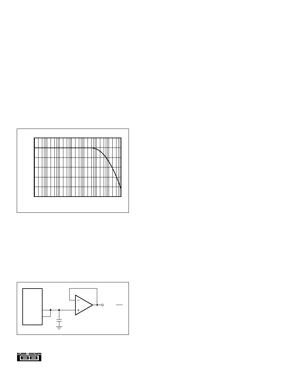
The output amplifiers include a RC continuous-time filter,
which helps to reduce the out-of-band noise energy present
at the DAC outputs due to the noise shaping characteristics
of the PCM1600's delta-sigma D/A converters. The fre-
quency response of this filter is shown in Figure 11. By
itself, this filter is not enough to attenuate the out-of-band
noise to an acceptable level for most applications. An
external low-pass filter is required to provide sufficient out-
of-band noise rejection. Further discussion of DAC post-
filter circuits is provided in the Applications Information
section of this data sheet.
FIGURE 11. Output Filter Frequency Response.
+
OPA337
10
µ
F
V
COM
1
V
COM
2
PCM1600
PCM1601
16
15
4
3
1
V
BIAS
V
CC
2
FIGURE 12. Biasing External Circuits Using the V
COM
1
and V
COM
2 Pins.
V
COM
1 AND V
COM
2 OUTPUTS
Two unbuffered common-mode voltage output pins, V
COM
1
(pin 16) and V
COM
2 (pin 15), are brought out for decoupling
purposes. These pins are nominally biased to a DC voltage
level equal to V
CC
/2. If these pins are to be used to bias
external circuitry, a voltage follower is required for buffer-
ing purposes. Figure 12 shows an example of using the
V
COM
1 and V
COM
2 pins for external biasing applications.
ZERO FLAG AND INFINITE ZERO DETECT MUTE
FUNCTIONS
The PCM1600 includes circuitry for detecting an all `0' data
condition for the data input pins, DATA1 through DATA3.
This includes two independent functions: Zero Output Flags
and Zero Detect Mute.
Although the flag and mute functions are independent of one
another, the zero detection mechanism is common to both
functions.
Zero Detect Condition
Zero Detection for each output channel is independent from
the others. If the data for a given channel remains at a `0'
level for 1024 sample periods (or LRCK clock periods), a
Zero Detect condition exists for the that channel.
Zero Output Flags
Given that a Zero Detect condition exists for one or more
channels, the Zero flag pins for those channels will be set to
a logic `1'state. There are Zero Flag pins for each channel,
ZERO1 through ZERO6 (pins 1 through 6). In addition, all
six Zero Flags are logically ANDed together and the result
provided at the ZEROA pin (pin 48), which is set to a logic
`1' state when all channels indicate a zero detect condition.
The Zero Flag pins can be used to operate external mute
circuits, or used as status indicators for a microcontroller,
audio signal processor, or other digitally controlled func-
tions.
Infinite Zero Detect Mute
Infinite Zero Detect Mute is an internal logic function. The
Zero Detect Mute can be enabled or disabled using the INZD
bit of Control Register 8. The reset default is Zero Detect
Mute disabled, INZD = 0. Given that a Zero Detect Condi-
tion exists for one or more channels, the zero mute circuitry
will immediately force the corresponding DAC output(s) to
the bipolar zero level, or V
CC
/2. This is accomplished by
switching the input of the DAC output amplifier from the
delta-sigma modulator output to the DC common-mode
reference voltage.
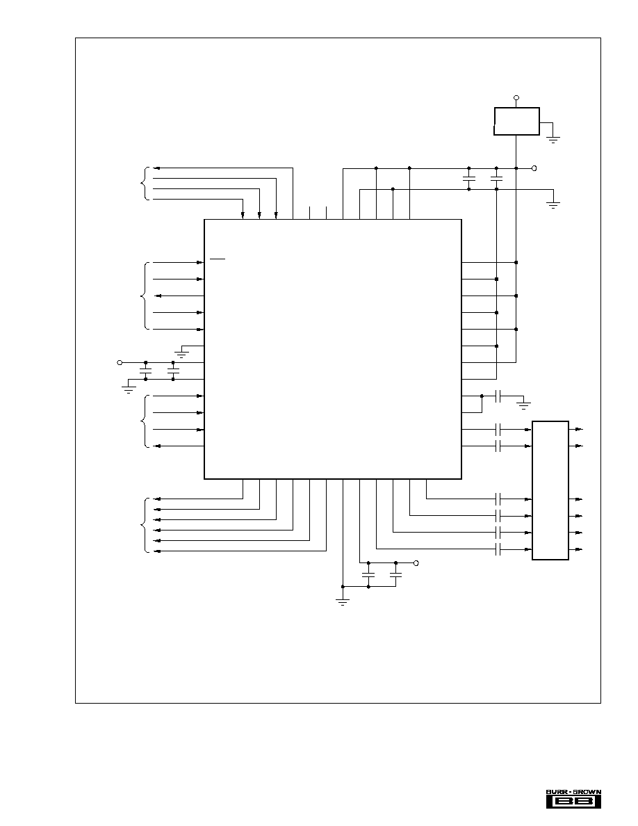
APPLICATIONS INFORMATION
CONNECTION DIAGRAMS
A basic connection diagram is shown in Figure 13, with the
necessary power supply bypassing and decoupling compo-
nents. Burr-Brown recommends using the component values
shown in Figure 13 for all designs.
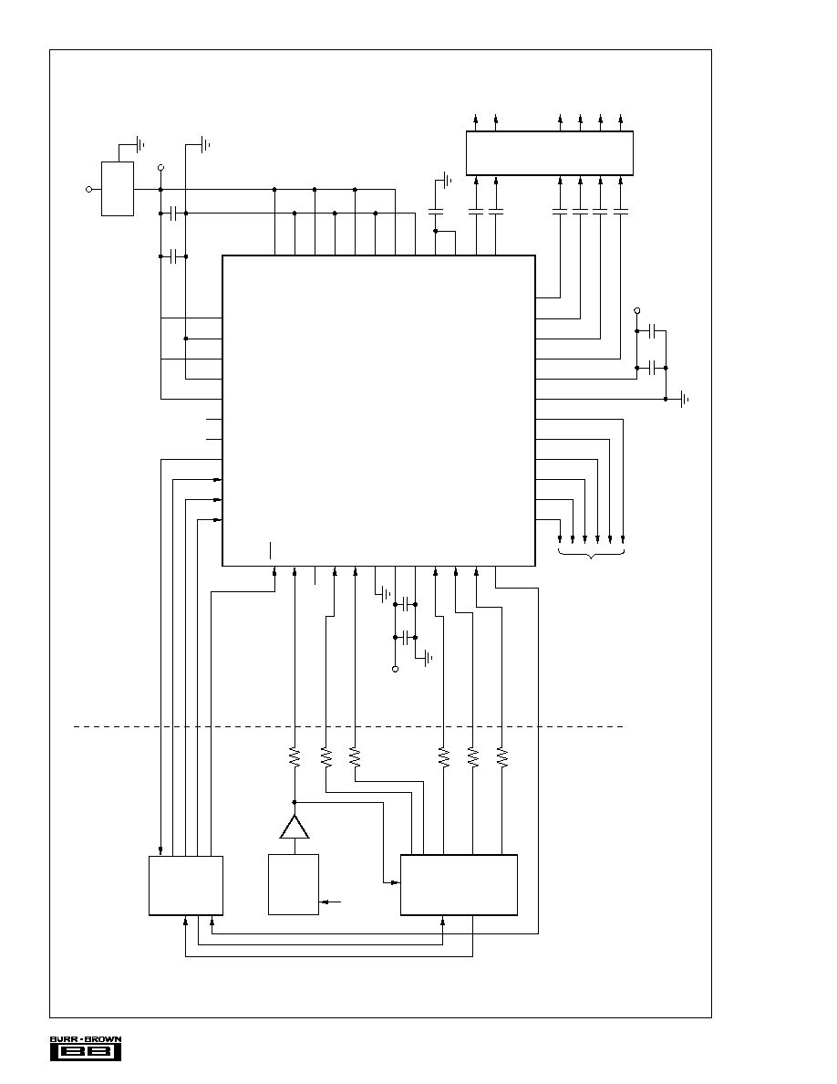
A typical application diagram is shown in Figure 14. Burr-
Brown's REG1117-3.3 is used to generate +3.3V for V
DD
from the +5V analog power supply. Burr-Brown's PLL1700E
is used to generate the system clock input at SCLKI, as well
as generating the clock for the audio signal processor.
The use of series resistors (22
to 100
) are recommended
for SCLKI, LRCK, BCK, DATA1, DATA2, and DATA3.
The series resistor combines with the stray PCB and device
input capacitance to form a low-pass filter which removes
high frequency noise from the digital signal, thus reducing
high frequency emission.
1
10
100
1k
10k
100k
10M
1M
20
0
≠20
≠40
≠60
≠80
≠100
Level (dB)
Log Frequency (Hz)
Æ
23
PCM1600, PCM1601
24
23
22
21
20
19
18
17
16
15
14
13
37
38
39
40
41
42
43
44
45
46
47
48
ZERO1
ZERO2
ZERO3
ZERO4
ZERO5
ZERO6
AGND
V
CC
V
OUT
6
V
OUT
5
V
OUT
4
V
OUT
3
ML
MC
MDI
MDO
NC
NC
V
CC
0
AGND0
V
CC
1
AGND1
V
CC
2
AGND2
RST
SCLKI
SCLKO
BCK
LRCK
TEST
V
DD
DGND
DATA1
DATA2
DATA3
ZEROA
V
CC
3
AGND3
V
CC
4
AGND4
V
CC
5
AGND5
V
CC
6
AGND6
V
COM
1
V
COM
2
V
OUT
1
V
OUT
2
36
35
34
33
32
31
30
29
28
27
26
1
2
3
4
5
6
7
8
9
10
11
25
12
PCM1600
PCM1601
+
To/From
Decoder
To/From
Decoder
or
Microcontroller
+3.3V
Analog
+5V Analog
+5V Analog
C
11
C
10
+
C
12
C
13
+
C
9
C
8
C
4
C
4
C
6
C
7
+
C
3
+
C
2
+
C
1
+
+
+
+
To/From
Decoder
Zero
Output
Flags
+3.3V
Regulator
+3.3V
Analog
Output
Low-Pass
Filters
NOTE: C
1
- C
7
, C
8
, C
11
, C
13
= 10
µ
F tantalum or aluminum electrolytic
C
9
, C
10
, C
12
= 0.1
µ
F ceramic
FIGURE 13. Basic Connection Diagram.
Æ
24
PCM1600, PCM1601
FIGURE 14. Typical Application Diagram.
24
23
22
21
20
19
18
17
16
15
14
13
37
38
39
40
41
42
43
44
45
46
47
48
ZERO1
ZERO2
ZERO3
ZERO4
ZERO5
ZERO6
AGND
V
CC
V
OUT
6
V
OUT
5
V
OUT
4
V
OUT
3
ML
MC
MDI
MDO
NC
NC
V
CC
0
AGND0
V
CC
1
AGND1
V
CC
2
AGND2
RST
SCLKI
SCLKO
BCK
LRCK
TEST
V
DD
DGND
DATA1
DATA2
DATA3
ZEROA
V
CC
3
AGND3
V
CC
4
AGND4
V
CC
5
AGND5
V
CC
6
AGND6
V
COM
1
V
COM
2
V
OUT
1
V
OUT
2
36
35
34
33
32
31
30
29
28
27
26
123456789
1
0
1
1
25
12
PCM1600
PCM1601
27MHz
Master Clock
Buffer
SCKO3
(2)
XT1
+5V Analog
+5V Analog
R
S
(3)
R
S
R
S
R
S
+
0.1
µ
F1
0
µ
F
+
10
µ
F
0.1
µ
F
10
µ
F
10
µ
F
10
µ
F
10
µ
F
10
µ
F
10
µ
F
+
+
+
+
+
+
+
Zero Flag Outputs
for Mute Circuits,
microcontroller, or
DSP/Decoder.
NOTES: (1) Serial Control and Reset functions may be provided
by DSP/Decoder GPIO pins. (2) Actual clock output used is determined
by the application. (3) R
S
= 22
to 100
. (4) See Applications Information
section of this data sheet for more information.
REG1117
+3.3V
+3.3V
Analog
Output
Low-Pass
Filters
(4)
LS
RS
CTR
SUB
LF
RF
R
S
R
S
µ
C/
µ
P
(1)
PLL1700
Audio DSP
or
Decoder
DIGITAL SECTION
ANALOG SECTION
+
+3.3V
Analog
C
11
C
10
Æ
25
PCM1600, PCM1601
POWER SUPPLIES AND GROUNDING
The PCM1600 requires a +5V analog supply and a +3.3V
digital supply. The +5V supply is used to power the DAC
analog and output filter circuitry, while the +3.3V supply is
used to power the digital filter and serial interface circuitry.
For best performance, the +3.3V supply should be derived
from the +5V supply using a linear regulator, as shown in
Figure 14.
Six capacitors are required for supply bypassing, as shown
in Figure 13. These capacitors should be located as close as
possible to the PCM1600 or PCM1601 package. The 10
µ
F
capacitors should be tantalum or aluminum electrolytic,
while the 0.1
µ
F capacitors are ceramic (X7R type is recom-
mended for surface-mount applications).
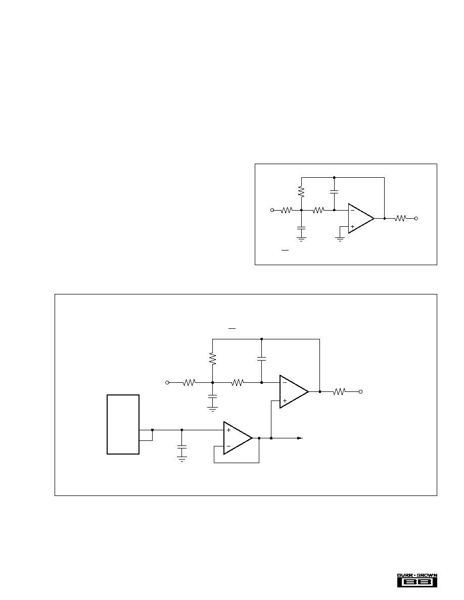
D/A OUTPUT FILTER CIRCUITS
Delta-sigma D/A converters utilize noise shaping techniques
to improve in-band Signal-to-Noise Ratio (SNR) perfor-
mance at the expense of generating increased out-of-band
noise above the Nyquist Frequency, or f
S
/2. The out-of-band
noise must be low-pass filtered in order to provide the
optimal converter performance. This is accomplished by a
combination of on-chip and external low-pass filtering.
Figures 15 and 16 show the recommended external low-pass
active filter circuits for dual and single-supply applications.
These circuits are 2nd-order Butterworth filters using the
Multiple Feedback (MFB) circuit arrangement, which re-
duces sensitivity to passive component variations over fre-
quency and temperature. For more information regarding
MFB active filter design, please refer to Burr-Brown Appli-
cations Bulletin AB-034, available from our web site
(www.burr-brown.com) or your local Burr-Brown sales
office.
Since the overall system performance is defined by the
quality of the D/A converters and their associated analog
output circuitry, high quality audio op amps are recom-
mended for the active filters. Burr-Brown's OPA2134 and
OPA2353 dual op amps are shown in Figures 15 and 16, and
are recommended for use with the PCM1600 and PCM1601.
FIGURE 15. Dual Supply Filter Circuit.
FIGURE 16. Single-Supply Filter Circuit.
R
1
R
3
R
4
R
2
C
1
C
2
V
IN
V
OUT
OPA2134
2
3
1
R
2
R
1
A
V
≠
R
1
R
3
R
4
R
2
C
1
C
2
V
IN
V
OUT
To Additional
Low-Pass Filter
Circuits
OPA2134
2
3
1
+
OPA337
C
2
10
µ
F
V
COM
1
V
COM
2
PCM1600
PCM1601
R
2
R
1
A
V
≠
Æ
26
PCM1600, PCM1601
Separate power supplies are recommended for the digital
and analog sections of the board. This prevents the switching
noise present on the digital supply from contaminating the
analog power supply and degrading the dynamic perfor-
mance of the D/A converters. In cases where a common +5V
supply must be used for the analog and digital sections, an
inductance (RF choke, ferrite bead) should be placed be-
tween the analog and digital +5V supply connections to
avoid coupling of the digital switching noise into the analog
circuitry. Figure 18 shows the recommended approach for
single-supply applications.
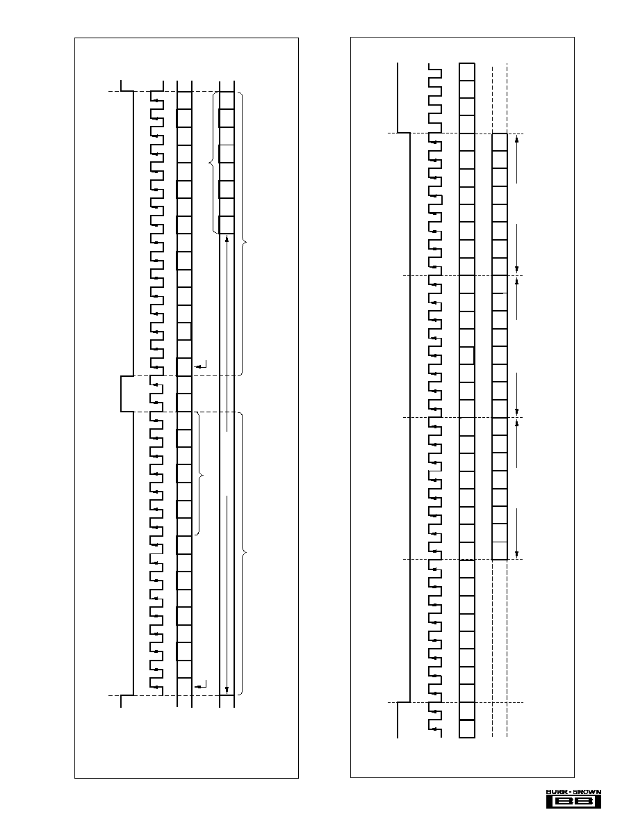
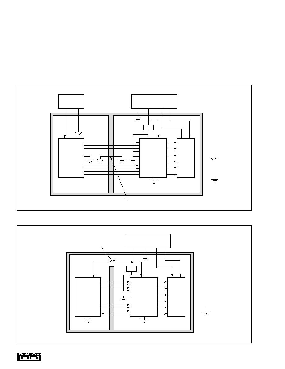
PCB LAYOUT GUIDELINES
A typical PCB floor plan for the PCM1600 and PCM1601 is
shown in Figure 17. A ground plane is recommended, with
the analog and digital sections being isolated from one
another using a split or cut in the circuit board. The PCM1600
or PCM1601 should be oriented with the digital I/O pins
facing the ground plane split/cut to allow for short, direct
connections to the digital audio interface and control signals
originating from the digital section of the board.
FIGURE 17. Recommended PCB Layout.
FIGURE 18. Single-Supply PCB Layout.
PCM1600
PCM1601
V
CC
V
DD
DGND
Return Path for Digital Signals
Analog
Ground
Digital
Ground
AGND
Output
Circuits
DIGITAL SECTION
ANALOG SECTION
Digital Logic
and
Audio
Processor
Digital Power
+V
D
DGND
Analog Power
+5VA
+V
S
AGND
REG
≠V
S
PCM1600
PCM1601
V
CC
V
DD
DGND
Output
Circuits
RF Choke or Ferrite Bead
Common
Ground
AGND
DIGITAL SECTION
ANALOG SECTION
V
DD
Power Supplies
+5V
+V
S
AGND
REG
≠V
S
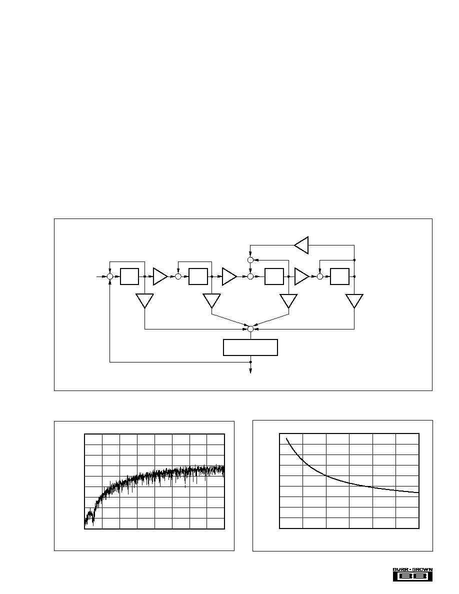
Æ
27
PCM1600, PCM1601
0
1
2
3
4
5
6
7
8
0
≠20
≠40
≠60
≠80
≠100
≠120
≠140
≠160
≠180
Amplitude (dB)
Frequency (f
S
)
FIGURE 20. Quantization Noise Spectrum.
0
100
200
300
400
500
600
125
120
115
110
105
100
95
90
85
80
Dynamic Range (dB)
Jitter (ps)
CLOCK JITTER
FIGURE 21. Jitter Sensitivity.
FIGURE 19. Eight-Level Delta-Sigma Modulator.
THEORY OF OPERATION
The delta-sigma section of PCM1600 is based on a 8-level
amplitude quantizer and a 4th-order noise shaper. This
section converts the oversampled input data to 8-level delta-
sigma format.
A block diagram of the 8-level delta-sigma modulator is
shown in Figure 19. This 8-level delta-sigma modulator has
the advantage of stability and clock jitter sensitivity over the
typical one-bit (2 level) delta-sigma modulator.
The combined oversampling rate of the delta-sigma modu-
lator and the internal 8x interpolation filter is 64f
S
for all
system clock combinations (256/384/512/768f
S
).
The theoretical quantization noise performance of the
8-level delta-sigma modulator is shown in Figure 20. The
enhanced multi-level delta-sigma architecture also has ad-
vantages for input clock jitter sensitivity due to the multi-
level quantizer, with the simulated jitter sensitivity shown in
Figure 21.
KEY PERFORMANCE PARAM-
ETERS AND MEASUREMENT
This section provides information on how to measure key
dynamic performance parameters for the PCM1600 and
PCM1601. In all cases, an Audio Precision System Two
Cascade or equivalent audio measurement system is utilized
to perform the testing.
TOTAL HARMONIC DISTORTION + NOISE
Total Harmonic Distortion + Noise (THD+N) is a significant
figure of merit for audio D/A converters, since it takes into
account both harmonic distortion and all noise sources
within a specified measurement bandwidth. The true rms
value of the distortion and noise is referred to as THD+N.
For the PCM1600 and PCM1601 D/A converters, THD+N is
measured with a full scale, 1kHz digital sine wave as the test
stimulus at the input of the DAC. The digital generator is set
+
Z
≠1
8-Level Quantizer
+
Z
≠1
+
Z
≠1
≠
+
Z
≠1
+
+
8f
S
64f
S

Æ
28
PCM1600, PCM1601
FIGURE 22. Test Setup for THD+N Measurements.
to 24-bit audio word length and a sampling frequency of
44.1kHz, or 96kHz. The digital generator output is taken
from the unbalanced S/PDIF connector of the measurement
system. The S/PDIF data is transmitted via coaxial cable to
the digital audio receiver on the DEM-DAI1600 demo board.
The receiver is then configured to output 24-bit data in either
I
2
S or left-justified data format. The DAC audio interface
format is programmed to match the receiver output format.
The analog output is then taken from the DAC post filter and
connected to the analog analyzer input of the measurment
system. The analog input is band limited using filters resi-
dent in the analyzer. The resulting THD+N is measured by
the analyzer and displayed by the measurement system.
DYNAMIC RANGE
Dynamic range is specified as A-Weighted, THD+N mea-
sured with a ≠60dBFS, 1kHz digital sine wave stimulus at
the input of the D/A converter. This measurment is designed
to give a good indicator of how the DAC will perform given
a low-level input signal.
The measurement setup for the dynamic range measurement
is shown in Figure 23, and is similar to the THD+N test
setup discussed previously. The differences include the band
limit filter selection, the additional A-Weighting filter, and
the ≠60dBFS input level.
IDLE CHANNEL SIGNAL-TO-NOISE RATIO
The SNR test provides a measure of the noise floor of the
D/A converter. The input to the D/A is all 0's data, and the
D/A converter's Infinite Zero Detect Mute function must
be disabled (default condition at power up for the PCM1600,
PCM1601). This ensures that the delta-sigma modulator
output is connected to the output amplifier circuit so that
idle tones (if present) can be observed and effect the SNR
measurement. The dither function of the digital generator
must also be disabled to ensure an all `0's data stream at the
input of the D/A converter.
The measurement setup for SNR is identical to that used for
dynamic range, with the exception of the input signal level.
(see the notes provided in Figure 23).
FIGURE 23. Test Set-Up for Dynamic Range and SNR Meeasurements.
S/PDIF
Receiver
Evaluation Board
f
≠3dB
= 54kHz
PCM1600
PCM1601
DEM-DAI1600
2nd-Order
Low-Pass
Filter
Notch Filter
Band Limit
HPF = 22Hz
(1)
LPF = 30kHz
(1)
f
C
= 1kHz
RMS Mode
100% Full Scale
24-Bit, 1kHz
Sine Wave
S/PDIF
Output
Option = 20kHz Apogee Filter
(2)
Analyzer
and
Display
Digital
Generator
NOTES: (1) There is little difference
in measured THD+N when using the
various settings for these filters.
(2) Required for THD+N test.
S/PDIF
Receiver
Evaluation Board
PCM1600
(1)
PCM1601
DEM-DAI1600
2nd-Order
Low-Pass
Filter
Notch Filter
Band Limit
HPF = 22Hz
LPF = 22kHz
f
C
= 1kHz
f
≠3dB
= 54kHz
0% Full Scale,
Dither Off (SNR)
≠60dBFS,
1kHz Sine Wave
(Dynamic Range)
S/PDIF
Output
Option = A-Weighting
(2)
A-Weight
Filter
(1)
RMS Mode
Analyzer
and
Display
Digital
Generator
NOTES: (1) Infinite Zero Detect Mute disabled.
(2) Results without A-Weighting will be
approximately 3dB worse.
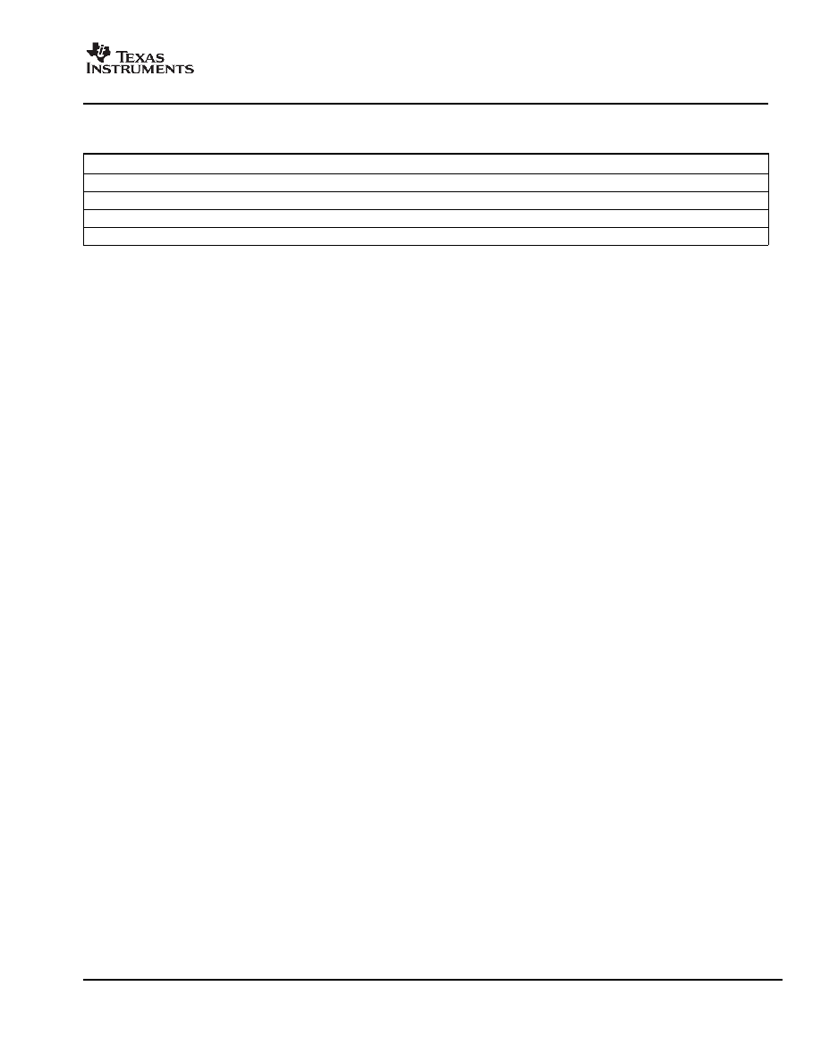
PACKAGING INFORMATION
ORDERABLE DEVICE
STATUS(1)
PACKAGE TYPE
PACKAGE DRAWING
PINS
PACKAGE QTY
PCM1600Y
ACTIVE
LQFP
PT
48
250
PCM1600Y/2K
ACTIVE
LQFP
PT
48
2000
PCM1601Y
ACTIVE
QFP
PJS
48
84
PCM1601Y/1K
ACTIVE
QFP
PJS
48
1000
(1) The marketing status values are defined as follows:
ACTIVE: Product device recommended for new designs.
LIFEBUY: TI has announced that the device will be discontinued, and a lifetime-buy period is in effect.
NRND: Not recommended for new designs. Device is in production to support existing customers, but TI does not recommend using this part in
a new design.
PREVIEW: Device has been announced but is not in production. Samples may or may not be available.
OBSOLETE: TI has discontinued the production of the device.
PACKAGE OPTION ADDENDUM
www.ti.com
3-Oct-2003

IMPORTANT NOTICE
Texas Instruments Incorporated and its subsidiaries (TI) reserve the right to make corrections, modifications,
enhancements, improvements, and other changes to its products and services at any time and to discontinue
any product or service without notice. Customers should obtain the latest relevant information before placing
orders and should verify that such information is current and complete. All products are sold subject to TI's terms
and conditions of sale supplied at the time of order acknowledgment.
TI warrants performance of its hardware products to the specifications applicable at the time of sale in
accordance with TI's standard warranty. Testing and other quality control techniques are used to the extent TI
deems necessary to support this warranty. Except where mandated by government requirements, testing of all
parameters of each product is not necessarily performed.
TI assumes no liability for applications assistance or customer product design. Customers are responsible for
their products and applications using TI components. To minimize the risks associated with customer products
and applications, customers should provide adequate design and operating safeguards.
TI does not warrant or represent that any license, either express or implied, is granted under any TI patent right,
copyright, mask work right, or other TI intellectual property right relating to any combination, machine, or process
in which TI products or services are used. Information published by TI regarding third-party products or services
does not constitute a license from TI to use such products or services or a warranty or endorsement thereof.
Use of such information may require a license from a third party under the patents or other intellectual property
of the third party, or a license from TI under the patents or other intellectual property of TI.
Reproduction of information in TI data books or data sheets is permissible only if reproduction is without
alteration and is accompanied by all associated warranties, conditions, limitations, and notices. Reproduction
of this information with alteration is an unfair and deceptive business practice. TI is not responsible or liable for
such altered documentation.
Resale of TI products or services with statements different from or beyond the parameters stated by TI for that
product or service voids all express and any implied warranties for the associated TI product or service and
is an unfair and deceptive business practice. TI is not responsible or liable for any such statements.
Following are URLs where you can obtain information on other Texas Instruments products and application
solutions:
Products
Applications
Amplifiers
amplifier.ti.com
Audio
www.ti.com/audio
Data Converters
dataconverter.ti.com
Automotive
www.ti.com/automotive
DSP
dsp.ti.com
Broadband
www.ti.com/broadband
Interface
interface.ti.com
Digital Control
www.ti.com/digitalcontrol
Logic
logic.ti.com
Military
www.ti.com/military
Power Mgmt
power.ti.com
Optical Networking
www.ti.com/opticalnetwork
Microcontrollers
microcontroller.ti.com
Security
www.ti.com/security
Telephony
www.ti.com/telephony
Video & Imaging
www.ti.com/video
Wireless
www.ti.com/wireless
Mailing Address:
Texas Instruments
Post Office Box 655303 Dallas, Texas 75265
Copyright
2003, Texas Instruments Incorporated