49%
FPO
Stereo Audio
DIGITAL-TO-ANALOG CONVERTER
PCM1710U
Æ
FEATURES
q
COMPLETE STEREO DAC:
8X Oversampling Digital Filter
Multi-Level Delta-Sigma DAC
Analog Low Pass Filter
Output Amplifier
q
HIGH PERFORMANCE:
≠92dB THD+N
98dB Dynamic Range
110dB SNR
q
ACCEPTS 16 OR 20 BITS INPUT DATA
q
SYSTEM CLOCK: 256fs or 384fs
q
SINGLE +5V POWER SUPPLY
q
ON-CHIP DIGITAL FILTER:
Soft Mute and Attenuator
Digital De-emphasis
Double-Speed Dubbing Mode
q
SMALL 28-PIN SOIC PACKAGE
DESCRIPTION
The PCM1710 is a complete stereo audio digital-to-
analog converter, including digital interpolation filter,
delta-sigma DAC, and analog voltage output. PCM1710
can accept either 16-bit normal or 20-Bit normal input
data (MSB first, right justified), or 16-bit IIS data
(32-bits per word, continuous clock).
The digital filter performs an 8X interpolation func-
tion, as well as special functions such as soft mute,
digital attenuation, de-emphasis and double-speed
dubbing. Performance of the digital feature is excel-
lent, featuring ≠62dB stop band attenuation and
±
0.008dB ripple in the pass band.
PCM1710 is suitable for a wide variety of consumer
applications where good performance is required.
Its low cost, small size and single +5V power supply
make it ideal for automotive CD players, bookshelf
CD players, BS tuners, keyboards, MPEG audio,
MIDI applications, set-top boxes, CD-ROM drives,
CD-Interactive and CD-Karaoke systems.
International Airport Industrial Park ∑ Mailing Address: PO Box 11400 ∑ Tucson, AZ 85734 ∑ Street Address: 6730 S. Tucson Blvd. ∑ Tucson, AZ 85706
Tel: (520) 746-1111 ∑ Twx: 910-952-1111 ∑ Cable: BBRCORP ∑ Telex: 066-6491 ∑ FAX: (520) 889-1510 ∑ Immediate Product Info: (800) 548-6132
Digital In
Input Interface
and
Attentuator
Oversampling
Digital Filter
4th-Order
Multi-Level
Delta
Sigma
DAC
Low-Pass
Filter
Output
Op Amp
Mode Control
System Clock
Lch OUT
Rch OUT
© 1994 Burr-Brown Corporation
PDS-1217B
Printed in U.S.A. June, 1995
SBAS030

Æ
PCM1710U
2
SPECIFICATIONS
All specifications at +25
∞
C, +V
CC
= +V
DD
= +5V, f
S
= 44.1kHz, f
SYS
= 384/256fs, and 16-bit data, unless otherwise noted.
The information provided herein is believed to be reliable; however, BURR-BROWN assumes no responsibility for inaccuracies or omissions. BURR-BROWN assumes
no responsibility for the use of this information, and all use of such information shall be entirely at the user's own risk. Prices and specifications are subject to change
without notice. No patent rights or licenses to any of the circuits described herein are implied or granted to any third party. BURR-BROWN does not authorize or warrant
any BURR-BROWN product for use in life support devices and/or systems.
PCM1710U
PARAMETER
CONDITIONS
MIN
TYP
MAX
UNITS
RESOLUTION
16
20
Bits
DIGITAL INPUT
Logic Family
Input Logic Level (except XTI)
V
IH
2.0
VDC
V
IL
0.8
VDC
Input Logic Current (except XTI)
≠200
µ
A
Input Logic Level (XTI)
V
IH
3.2
VDC
V
IL
1.4
VDC
Input Logic Current (XTI)
±
50
µ
A
Output Logic Level (CLKO):
V
OH
4.5
VDC
V
OL
0.5
VDC
Output Logic Current (CLKO)
±
10
mA
Data Format
Normal (16/20-bit)/IIS (16-bit) selectable
Sampling Frequency
32
44.1
48
kHz
System Clock Frequency
384f
S
12.288
16.934
18.432
MHz
System Clock Frequency
256f
S
8.192
11.2894
12.288
MHz
DC ACCURACY
Gain Error
±
1.0
±
5.0
% of FSR
Gain Mis-Match Channel-To-Channel
±
1.0
±
5.0
% of FSR
Bipolar Zero Error
V
O
= 1/2V
CC
at Bipolar Zero
±
20.0
mV
Gain Drift
±
50
ppm of FSR/
∞
C
Bipolar Gain Drift
±
20
ppm of FSR/
∞
C
DYNAMIC PERFORMANCE
(1)
THD+N at F/S (0dB)
(2)
f
IN
= 991kHz
≠92
≠88
dB
THD+N at ≠60fdB
(2)
f
IN
= 991kHz
≠36
≠32
dB
Dynamic Range
EIAJ A-weighted
98
dB
S/N Ratio
EIAJ A-weighted
104
110
dB
Channel Separation
90
94
dB
DIGITAL FILTER PERFORMANCE
Pass Band Ripple
Normal Mode
±
0.008
dB
Pass Band Ripple
Double Speed Mode
±
0.018
dB
Stop Band Attenuation
Normal Mode
≠62
dB
Stop Band Attenuation
Double Speed Mode
≠58
dB
Pass Band
Normal Mode
0.4535
fs
Pass Band
Double Speed Mode
0.4535
fs
Stop Band
Normal Mode
0.5465
fs
Stop Band
Double Speed Mode
0.5465
fs
De-emphasis Error
(f
S
32kHz ~ 48kHz)
≠0.05
+0.03
dB
ANALOG OUTPUT
Voltage Range
3.2
Vp-p
Load Impedance
5
k
Center Voltage
+1/2V
CC
V
POWER SUPPLY REQUIREMENTS
Voltage Range: +V
CC
+4.5
+5.0
+5.5
VDC
+V
DD
+4.5
+5.0
+5.5
VDC
Supply Current (+I
CC
) + (+I
DD
)
45
70
mA
TEMPERATURE RANGE
Operation
≠25
+85
∞
C
Storage
≠55
+100
∞
C
NOTE: (1) Dynamic performance specs are tested with external 20kHz low pass filter. (2) 30kHz LPF, 400Hz HPF, Average Mode. Shibusoku #725 THD Meter.
3
Æ
PCM1710U
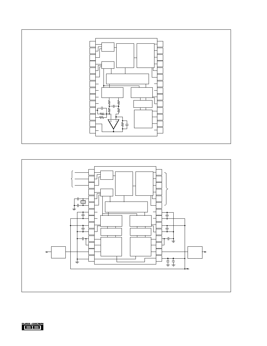
PIN ASSIGNMENTS
PIN NAME
NUMBER
FUNCTION
Input Interface Pins
LRCIN
1
Sample Rate Clock Input. Controls the update rate (fs).
DIN
2
Serial Data Input. MSB first, right justified format contains a frame of 16-bit or 20-bit data.
BCKIN
3
Bit Clock Input. Clocks in the data present on DIN input.
Mode Controls and Clock Signals
CLKO
4
Buffered Output of Oscillator. Equivalent to fs.
XTI
5
Oscillator Input (External Clock Input). For an internal clock, tie XTI to one side of the crystal oscillator. For an external clock,
tie XTI to the output of the chosen external clock.
XTO
6
Oscillator Output. When using the internal clock, tie to the opposite side (from pin 5) of the crystal oscillator. When using an
external clock, leave XTO open.
CKSL
23
System Clock Select. For 384fs, tie CKSL "High". For 256fs, tie CKSL "Low".
MODE
24
Operation Mode Select. For serial mode, tie MODE "High". For parallel mode, tie MODE "Low".
MUTE
25
Mute Control. To disable soft mute, tie MUTE "High". To enable soft mute, tie MUTE "Low".
MD/DM1
26
Mode Control for Data/De-emphasis. See "Mode Control Functions" on page 11.
MC/DM2
27
Mode Control for BCKIN/De-emphasis. See "Mode Control Functions" on page 11.
ML/DSD
28
Mode Control for WDCK/Double speed dubbing. See "Mode Control Functions" on page 11.
Analog Functions
V
OUT
R
13
Right Channel Analog Output.
V
OUT
L
16
Left Channel Analog Output.
Power Supply Connections
DGND
7, 22
Digital Ground.
V
DD
8, 21
Digital Power Supply (+5V).
V
CC
2R
9
Analog Power Supply (+5V), Right Channel DAC.
AGND2R
10
Analog Ground (DAC), Right Channel.
EXT1R
11
Output Amplifier Common, Right Channel. Bypass to ground with a 10
µ
F capacitor.
EXT2R
12
Output Amplifier Bias, Right Channel. Connect to EXT1R.
AGND
14
Analog Ground.
V
CC
15
Analog Power Supply (+5V).
EXT2L
17
Output Amplifier Bias, Left Channel. Connect to EXT1L.
EXT1L
18
Output Amplifier Common, Left Channel. Bypass to ground with a 10
µ
F capacitor.
AGND2L
19
Analog Ground (DAC), Left Channel.
V
CC
2L
20
Analog Power Supply (+5V), Left Channel DAC.
Power Supply Voltages ................................................................
±
6.5VDC
+V
CC
to V
DD
Voltage ..........................................................................
±
0.1V
Input Logic Voltage ..................................................... ≠0.3V to V
DD
+0.3V
Power Dissipation .......................................................................... 400mW
Operating Temperature Range ......................................... ≠25
∞
C to +85
∞
C
Storage Temperature Range .......................................... ≠55
∞
C to +125
∞
C
Lead Temperature (soldering, 5s) ................................................. +260
∞
C
ABSOLUTE MAXIMUM RATINGS
PACKAGE INFORMATION
PACKAGE DRAWING
MODEL
PACKAGE
NUMBER
(1)
PCM1710U
28-Pin SOIC
217
NOTE: (1) For detailed drawing and dimension table, please see end of data
sheet, or Appendix D of Burr-Brown IC Data Book.
Æ
PCM1710U
4
PIN CONFIGURATION
CONNECTION DIAGRAM
1
2
3
4
5
6
7
8
9
10
11
12
13
14
28
27
26
25
24
23
22
21
20
19
18
17
16
15
Input
Interface
Digital
Filter
Mode
Control
Timing
Control
Noise
Shaper
5-Level
DAC
Right
5-Level
DAC
Left
Low-Pass
Filter Left
Output
Amplifier
Left
Serial
Data Input
(2)
Mode Control
(3)
Low-Pass
Filter Right
Output
Amplifier
Right
NOTES: (1) Bypass Capacitor :1µF ~ 10µF.
(2) Input pins require pull-up resistors. (3) Mode
control pins require pull-up resistors.
10pF ~ 22pF x 2
10µF
Rch OUT
Lch OUT
+5V
Power Supply
10µF
100µF
+
+
+
≠
(1)
(1)
(1)
(1)
(1)
Post
Low Pass
Filter
Post
Low Pass
Filter
LRCIN
DIN
BCKIN
CLKO
XTI
XTO
DGND
V
DD
V
CC
2R
AGND2R
EXT1R
EXT2R
V
OUT
R
AGND1
ML/DSD
MC/DM2
MD/DM1
MUTE
MODE
CKSL
DGND
V
DD
V
CC
2L
AGND2L
EXT1L
EXT2L
V
OUT
L
V
CC
1
1
2
3
4
5
6
7
8
9
10
11
12
13
14
28
27
26
25
24
23
22
21
20
19
18
17
16
15
Input
Interface
Digital
Filter
Mode
Control
Timing
Control
Noise
Shaper
5-Level
DAC
Right
5-Level
DAC
Left
Low-Pass
Filter-Left
Output
Amplifier
Left
5
Æ
PCM1710U
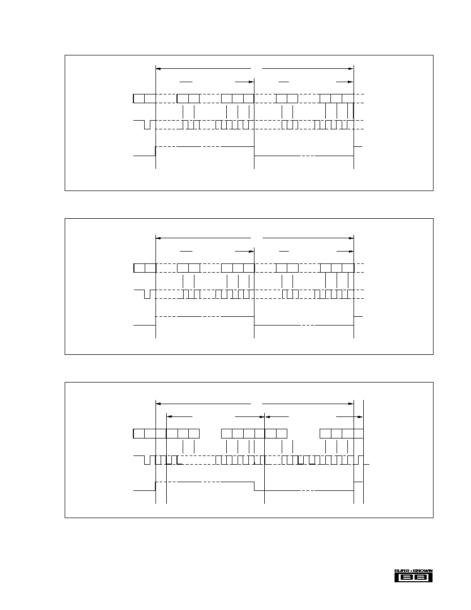
DATA INPUT TIMING
1
LRCIN
DIN
BCKIN
2
14
16
15
1
2
14
16
15
MSB
LSB
MSB
LSB
Left-channel Data
Right-channel Data
1 f/s
FIGURE 1. Normal Format, 16-Bit (LRCIN H: Lch).
FIGURE 2. Normal Format, 20-Bit (LRCIN H: Lch).
FIGURE 3. IIS Format, (16-Bit, 32 BCKIN Clock Cycles Per fs Interval).
1
LRCIN
DIN
BCKIN
2
18
20
19
1
2
18
20
19
MSB
LSB
MSB
LSB
Left-channel Data
Right-channel Data
1 f/s
1
LRCIN
DIN
BCKIN
2
13
16
14
1
2
13
15
14
MSB
LSB MSB
LSB
Left-channel Data
Right-channel Data
1 f/s
15
16
16
3