Æ
1
PCM1717
49%
FPO
PCM1717
Æ
Stereo Audio
DIGITAL-TO-ANALOG CONVERTER
FEATURES
q
ACCEPTS 16- OR 18-BIT INPUT DATA
q
COMPLETE STEREO DAC:
8X Oversampling Digital Filter
Multi-Level Delta-Sigma DAC
Analog Low Pass Filter
Output Amplifier
q
HIGH PERFORMANCE:
≠90dB THD+N
96dB Dynamic Range
100dB SNR
q
SYSTEM CLOCK: 256fs or 384fs
q
WIDE POWER SUPPLY: +2.7V to +5.5V
q
SELECTABLE FUNCTIONS:
Soft Mute
Digital Attenuation (256 Steps)
Digital De-emphasis
Output Mode: L, R, Mono, Mute
q
SMALL SSOP-20 PACKAGE
DESCRIPTION
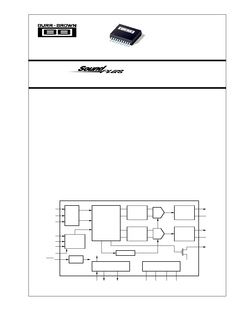
The PCM1717 is a complete low cost stereo, audio
digital-to-analog converter, including digital interpo-
lation filter, 3rd-order delta-sigma DAC, and analog
output amplifiers. PCM1717 is fabricated on a highly
advanced 0.6
µ
CMOS process. PCM1717 accepts
16- or 18-bit normal input data format, or 16- or
18-bit I
2
S data format.
The digital filter performs an 8X interpolation func-
tion, as well as special functions such as soft mute,
digital attenuation, and digital de-emphasis. The digi-
tal filter features ≠35dB stop band attenuation and
±
0.17dB ripple in the pass band.
PCM1717 is suitable for a wide variety of cost-sensitive
consumer applications where good performance is re-
quired. Its low cost, small size, and single +5V power
supply make it ideal for automotive CD players, book-
shelf CD players, BS tuners, keyboards, MPEG audio,
MIDI applications, set-top boxes, CD-ROM drives,
CD-Interactive, and CD-Karaoke systems.
Æ
PCM1717
Serial
Input
I/F
Mode
Control
I/F
8X Oversampling
Digital Filter with
Multi Function
Control
Clock/OSC Manager
XTI XTO
CLKO
V
CC
AGND
V
DD
DGND
Multi-level
Delta-Sigma
Modulator
V
OUT
L
D/C_L
Open Drain
DAC
Multi-level
Delta-Sigma
Modulator
Output Amp
and
Low-pass
Filter
Output Amp
and
Low-pass
Filter
BPZ-Cont.
V
OUT
R
D/C_R
ZERO
DAC
MC/DM0
MD/DM1
ML/MUTE
LRCIN
DIN
BCKIN
Reset
MODE
RSTB
Power Supply
© 1995 Burr-Brown Corporation
PDS-1289D
Printed in U.S.A. March, 2000
For most current data sheet and other product
information, visit www.burr-brown.com
International Airport Industrial Park ∑ Mailing Address: PO Box 11400, Tucson, AZ 85734 ∑ Street Address: 6730 S. Tucson Blvd., Tucson, AZ 85706 ∑ Tel: (520) 746-1111
Twx: 910-952-1111 ∑ Internet: http://www.burr-brown.com/ ∑ Cable: BBRCORP ∑ Telex: 066-6491 ∑ FAX: (520) 889-1510 ∑ Immediate Product Info: (800) 548-6132
SBAS038
Æ
2
PCM1717
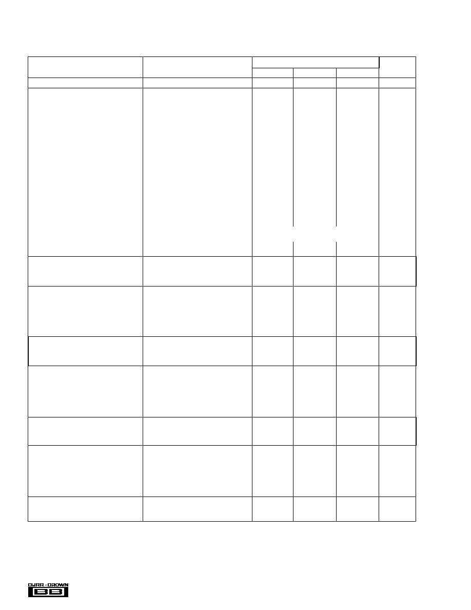
SPECIFICATIONS
All specifications at +25
∞
C, +V
CC
= +V
DD
= +5V, fs = 44.1kHz, and 16-bit input data, SYSCLK = 384fs, unless otherwise noted. Measurement bandwidth is 20kHz.
PCM1717E
PARAMETER
CONDITIONS
MIN
TYP
MAX
UNITS
RESOLUTION
16
18
Bits
DIGITAL INPUT/OUTPUT
Logic Family
CMOS
Input Logic Level:
V
IH
(2)
70% of V
DD
V
V
IL
(2)
30% of V
DD
V
V
IH
(3)
70% of V
DD
V
V
IL
(3)
30% of V
DD
V
V
IH
(4)
64% of V
DD
V
V
IL
(4)
28% of V
DD
V
Input Logic Current:
I
IH
(5)
≠6.0
µ
A
I
IL
(5)
≠120
µ
A
I
IH
(6)
≠2
µ
A
I
IL
(6)
0.02
µ
A
I
IH
(4)
V
IN
= 3.2V
40
µ
A
I
IL
(4)
V
IN
= 1.4V
≠40
µ
A
Output Logic Level: (+V
DD
= +5V)
V
OH
(7)
I
OH
= ≠5mA
3.8
V
V
OL
(7)
I
OL
= +5mA
1.0
V
V
OL
(8)
I
OL
= +5mA
1.0
V
Interface Format
Selectable Normal, I
2
S
Data Format
16/18 Bits MSB First Binary Two's Complement
Sampling Frequency
32
44.1
48
kHz
System Clock Frequency
256fs/384fs
8.192/12.288
11.2896/16.9344
12.288/18.432
MHz
DC ACCURACY
Gain Error
±
1.0
±
5.0
% of FSR
Gain Mismatch Channel-to-Channel
±
1.0
±
5.0
% of FSR
Bipolar Zero Error
V
O
= 1/2 V
CC
at Bipolar Zero
±
30
mV
DYNAMIC PERFORMANCE
(1)
V
CC
= +5V, f = 991Hz
THD+N at FS (0dB)
≠90
≠80
dB
THD+N at ≠60dB
≠34
dB
Dynamic Range
EIAJ, A-weighted
90
96
dB
Signal-To-Noise Ratio
EIAJ, A-weighted
92
100
dB
Channel Separation
90
97
dB
Level Linearity Error (≠90dB)
±
0.5
dB
DYNAMIC PERFORMANCE
(1)
V
CC
= +3V, f = 991Hz
THD+N at FS (0dB)
≠86
dB
Dynamic Range
EIAJ, A-weighted
91
dB
Signal-To-Noise Ratio
EIAJ, A-weighted
94
dB
DIGITAL FILTER PERFORMANCE
Pass Band Ripple
±
0.17
dB
Stop Band Attenuation
≠35
dB
Pass Band
0.445
fs
Stop Band
0.555
fs
De-emphasis Error
(fs = 32kHz ~ 48kHz)
≠0.2
+0.55
dB
Delay Time (Latency)
11.125/fs
sec
ANALOG OUTPUT
Voltage Range
FS (0dB) OUT
62% of V
CC
Vp-p
Load Impedance
5
k
Center Voltage
50% of V
CC
V
POWER SUPPLY REQUIREMENTS
Voltage Range:
+V
CC
+2.7
+5.5
VDC
+V
DD
+2.7
+5.5
VDC
Supply Current: +I
CC
+I
DD
(9)
+V
CC
= +V
DD
= +5V
18.0
25.0
mA
+V
CC
= +V
DD
= +3V
9.0
15.0
mA
Power Dissipation
+V
CC
= +V
DD
= +5V
90
125
mW
+V
CC
= +V
DD
= +3V
27
45
mW
TEMPERATURE RANGE
Operation
≠25
+85
∞
C
Storage
≠55
+100
∞
C
NOTES: (1) Tested with Shibasoku #725 THD. Meter 400Hz HPF, 30kHz LPF On, Average Mode with 20kHz bandwidth limiting. (2) Pins 4, 5, 6, 14: LRCIN, DIN,
BCKIN, FORMAT. (3) Pins 15, 16, 17, 18: RSTB, DM0, DM1, MUTE (Schmitt trigger input). (4) Pin 1: XTI. (5) Pins 15, 16, 17, 18: RSTB, DM0, DM1, MUTE (if
pull-up resistor is used). (6) Pins 4, 5, 6: LRCIN, DIN, BCKIN (if pull-up resistor is not used). (7) Pin 19: CLKO. (8) Pin 7: ZERO. (9) No load on pins 19 (CLKO)
and 20 (XTO).
Æ
3
PCM1717
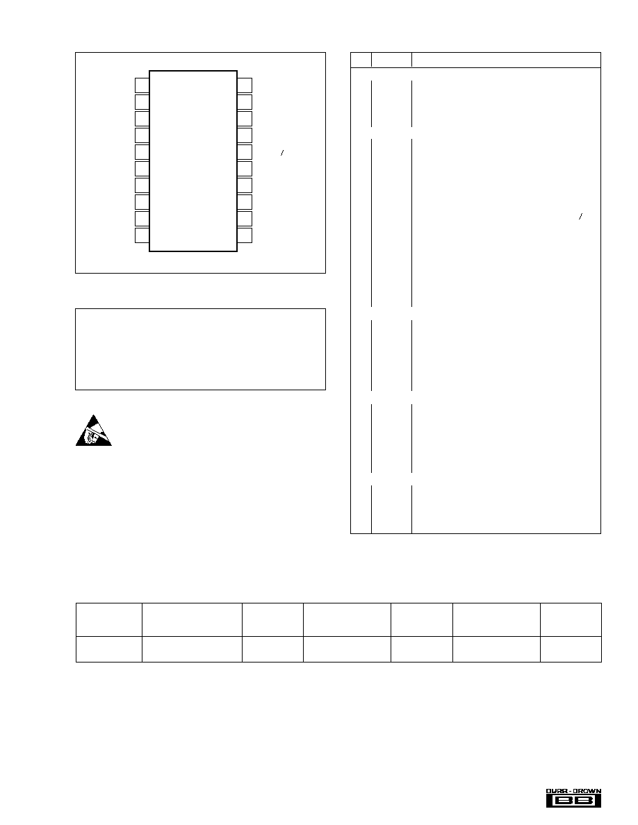
PIN ASSIGNMENTS
XTI
DGND
V
DD
LRCIN
DIN
BCKIN
ZERO
D/C_R
V
OUT
R
AGND
XTO
CLKO
ML/MUTE
MC/DM1
MD/DM0
RSTB
MODE
DC_L
V
OUT
L
V
CC
1
2
3
4
5
6
7
8
9
10
20
19
18
17
16
15
14
13
12
11
PIN CONFIGURATION
PIN
NAME
FUNCTION
Data Input Interface Pins
4
LRCIN
Sample Rate Clock Input. Controls the update rate (fs).
5
DIN
Serial Data Input. MSB first, right justified (Sony format)
or I
2
S (Philips). Contains a frame of 16- or 18-bit data.
6
BCKIN
Bit Clock Input. Clocks in the data present on DIN input.
Mode Control and Clock Signals
1
XTI
Oscillator Input (External Clock Input). For an internal
clock, tie XTI to one side of the crystal oscillator. For an
external clock, tie XTI to the output of the chosen
external clock.
14
MODE
Operation Mode Select. For Software Mode, tie Mode
"HIGH". For Hardware Mode, tie Mode "LOW".
16
MD/DM0
Mode Control for Data Input or De-emphasis. When
"HIGH" MD is selected, and a "LOW" selects DM0.
17
MC/DM1
Mode Control for BCKIN or De-emphasis. When "HIGH",
MC is selected, and a "LOW" selects DM1.
18
ML/MUTE
Mode Control for Strobe Clock or Mute. When "HIGH",
ML is selected, and a "LOW" selects mute.
19
CLKO
Buffered Output of Oscillator. Equivalent to XTI.
20
XTO
Oscillator Output. When using the internal clock, tie to
the opposite side (from pin 1) of the crystal oscillator.
When using an external clock, leave XTO open.
Operational Controls and Flags
7
ZERO
Infinite Zero Detection Flag, open drain output. When
the zero detection feature is muting the output, ZERO
is "LOW". When non-zero input data is present, ZERO
is in a high impedance state. When the input data is
continuously zero for 65.536 BCKIN cycles, zero will be
low.
15
RSTB
Resets DAC operation with an active "LOW" pulse.
Analog Output Functions
8
D/C_R
Right Channel Output Amplifier Common. Bypass to
ground with 10
µ
F capacitor.
9
V
OUT
R
Right Channel Analog Output. V
OUT
max = 0.62 x V
CC
.
12
V
OUT
L
Left Channel Analog Output. V
OUT
max = 0.62 x V
CC
.
13
D/C_L
Left Channel Output Amplifier Common. Bypass to
ground with 10
µ
F capacitor.
Power Supply Connections
2
DGND
Digital Ground.
3
V
DD
Digital Power Supply (+5V).
10
AGND
Analog Ground.
11
V
CC
Analog Power Supply (+3V).
The information provided herein is believed to be reliable; however, BURR-BROWN assumes no responsibility for inaccuracies or omissions. BURR-BROWN assumes no
responsibility for the use of this information, and all use of such information shall be entirely at the user's own risk. Prices and specifications are subject to change without notice.
No patent rights or licenses to any of the circuits described herein are implied or granted to any third party. BURR-BROWN does not authorize or warrant any BURR-BROWN
product for use in life support devices and/or systems.
Power Supply Voltage ...................................................................... +6.5V
+V
CC
to +V
DD
Difference ...................................................................
±
0.1V
Input Logic Voltage .................................................. ≠0.3V to (V
DD
+ 0.3V)
Power Dissipation .......................................................................... 200mW
Operating Temperature Range ......................................... ≠25
∞
C to +85
∞
C
Storage Temperature ...................................................... ≠55
∞
C to +125
∞
C
Lead Temperature (soldering, 5s) .................................................. +260
∞
C
Thermal Resistance,
JA .......................................................................................
+70
∞
C/W
ABSOLUTE MAXIMUM RATINGS
ELECTROSTATIC
DISCHARGE SENSITIVITY
This integrated circuit can be damaged by ESD. Burr-Brown
recommends that all integrated circuits be handled with
appropriate precautions. Failure to observe proper handling
and installation procedures can cause damage.
ESD damage can range from subtle performance degradation
to complete device failure. Precision integrated circuits may
be more susceptible to damage because very small parametric
changes could cause the device not to meet its published
specifications.
PACKAGE
SPECIFIED
DRAWING
TEMPERATURE
PACKAGE
ORDERING
TRANSPORT
PRODUCT
PACKAGE
NUMBER
RANGE
MARKING
NUMBER
(1)
MEDIA
PCM1717E
SSOP-20
334-1
≠25
∞
C to +85
∞
C
PCM1717E
PCM1717E
Rails
"
"
"
"
"
PCM1717E/2K
Tape and Reel
NOTE: (1) Models with a slash (/) are available only in Tape and Reel in the quantities indicated (e.g., /2K indicates 2000 devices per reel). Ordering 2000 pieces
of "PCM1717E/2K" will get a single 2000-piece Tape and Reel.
PACKAGE/ORDERING INFORMATION
Æ
4
PCM1717
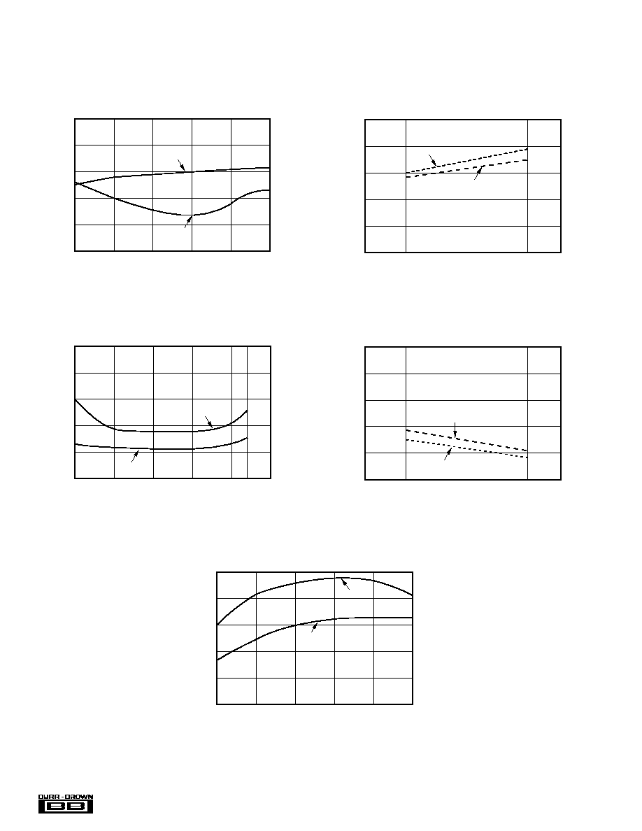
TYPICAL PERFORMANCE CURVES
At T
A
= +25
∞
C, +V
CC
= +V
DD
= +5V, fs = 44.1kHz, and 16-bit input data, SYSCLK = 384fs, unless otherwise noted.
DYNAMIC PERFORMANCE
THD+N vs TEMPERATURE
f
IN
= 1kHz, 384f
S
Temperature (∞C)
THD+N at FS (dB)
THD+N at ≠60dB (dB)
≠84
≠86
≠88
≠90
≠92
≠90
≠30
≠34
≠38
≠25
0
25
50
75
85
100
≠60dB
0dB
DYNAMIC RANGE vs INPUT DATA
f
IN
= 1kHz
Input Data
Dynamic Range (dB)
100
98
96
94
92
90
16-Bit
18-Bit
256f
S
384f
S
THD+N vs INPUT DATA
f
IN
= 1kHz, FS (0dB)
Input Data
THD+N (dB)
≠84
≠86
≠88
≠90
≠92
≠94
16-Bit
18-Bit
256f
S
384f
S
THD+N vs V
CC
, V
DD
f
IN
= 1kHz, 384f
S
V
CC
, V
DD
(V)
THD+N at FS (dB)
THD+N at ≠60dB (dB)
≠84
≠86
≠88
≠90
≠92
≠94
≠30
≠34
≠38
3.0
3.5
4.0
4.5
5.0
5.5
≠60dB
0dB
DYNAMIC RANGE AND SNR vs V
CC
, V
DD
f
IN
= 1kHz, 384f
S
V
CC
, V
DD
(dB)
100
98
96
94
92
90
3.0
3.5
4.0
4.5
5.0
5.5
SNR
Dynamic
Range
Æ
5
PCM1717
TYPICAL PERFORMANCE CURVES
At T
A
= +25
∞
C, +V
CC
= +V
DD
= +5V, fs = 44.1kHz, and 16-bit input data, SYSCLK = 384fs, unless otherwise noted.
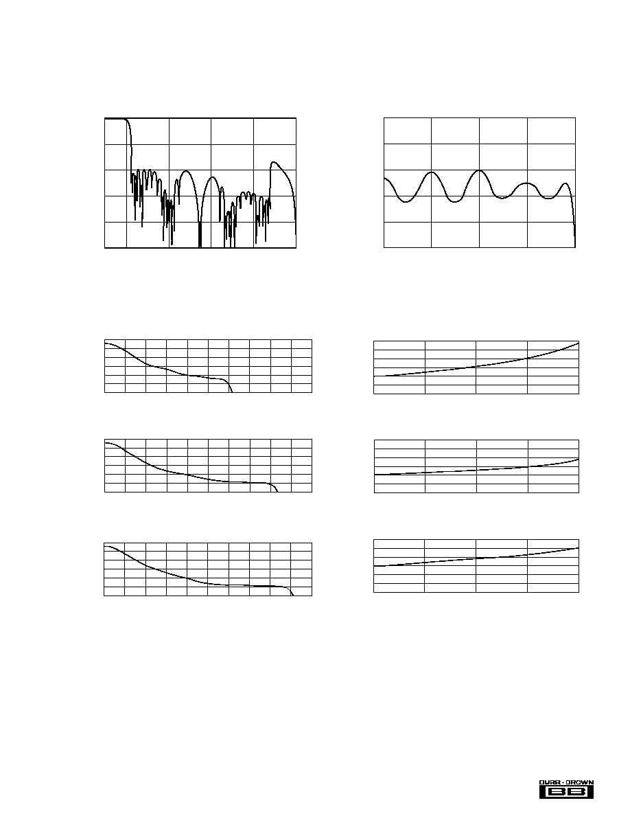
DIGITAL FILTER
0 0.4536f
S
1.3605f
S
2.2675f
S
3.1745f
S
4.0815f
S
0
≠20
≠40
≠60
≠80
≠100
dB
OVERALL FREQUENCY CHARACTERISTIC
Frequency (Hz)
0
5k
10k
15k
20k
25k
0
≠2
≠4
≠6
≠8
≠10
≠12
Level (dB)
Frequency (Hz)
DE-EMPHASIS FREQUENCY RESPONSE (32kHz)
DE-EMPHASIS FREQUENCY RESPONSE (44.1kHz)
0
≠2
≠4
≠6
≠8
≠10
≠12
Level (dB)
0
5k
10k
15k
20k
25k
Frequency (Hz)
DE-EMPHASIS FREQUENCY RESPONSE (48kHz)
0
≠2
≠4
≠6
≠8
≠10
≠12
Level (dB)
Frequency (Hz)
0
5k
10k
15k
20k
25k
PASSBAND RIPPLE CHARACTERISTIC
0
≠0.2
≠0.4
≠0.6
≠0.8
≠1
0
0.1134f
S
0.2268f
S
0.3402f
S
0.4535f
S
dB
Frequency (Hz)
0
3628
7256
10884
14512
0.6
0.4
0.2
0
≠0.2
≠0.4
≠0.6
Frequency (Hz)
DE-EMPHASIS ERROR (32kHz)
Error (dB)
0
4999.8375
9999.675
14999.5125
19999.35
0.6
0.4
0.2
0
≠0.2
≠0.4
≠0.6
Frequency (Hz)
DE-EMPHASIS ERROR (44.1kHz)
Error (dB)
0
5442
10884
16326
21768
0.6
0.4
0.2
0
≠0.2
≠0.4
≠0.6
Frequency (Hz)
DE-EMPHASIS ERROR (48kHz)
Error (dB)