PCM1730
SLES021 ≠ NOVEMBER 2001
24-BIT, 192-kHz SAMPLING ADVANCED SEGMENT, AUDIO
STEREO DIGITAL-TO-ANALOG CONVERTER
1
www.ti.com
FEATURES
D
24-Bit Resolution
D
Analog Performance (V
CC
= 5 V):
≠ Dynamic Range: 117 dB (Typically)
≠ SNR: 117 dB (Typically)
≠ THD+N: 0.0004% (Typically)
≠ Full-Scale Output (At Post Amp): 2.2-Vrms
D
Differential Current Output:
±
2.48 mA
D
8
◊
Oversampling Digital Filter:
≠ Stop-Band Attenuation: ≠82 dB
≠ Pass-Band Ripple:
±
0.002 dB
D
Sampling Frequency of 10 kHz to 200 kHz
D
System Clock: 128, 192, 256, 384, 512, or
768 f
S
With Auto Detect
D
Accepts 16-, 20-, and 24-Bit Audio Data
D
Data Formats: Standard, I
2
S, and
Left-Justified
D
Digital De-Emphasis
D
Soft Mute
D
Zero Flags for Each Output
D
Dual Supply Operation:
≠ 5 V for Analog
≠ 3.3 V for Digital
D
5-V Tolerant Digital Inputs
D
Small 28-Lead SSOP Package
APPLICATIONS
D
A/V Receivers
D
DVD Movie Players
D
SACD Player
D
HDTV Receivers
D
Car Audio Systems
D
Digital Multi-Track Recorders
D
Other Applications Requiring 24-Bit Audio
DESCRIPTION
The PCM1730 is a CMOS, monolithic integrated circuit
that includes stereo digital-to-analog converters and
support circuitry in a small 28-lead SSOP package. The
data converters utilize Texas Instruments' advanced
segment DAC architecture to achieve excellent
dynamic performance and improved tolerance to clock
jitter. The PCM1730 provides balanced current outputs,
allowing the user to optimize analog performance
externally. Sampling rates up to 200 kHz are supported.
PACKAGE/ORDERING INFORMATION
PRODUCT
PACKAGE
PACKAGE
DRAWING
NUMBER
OPERATING
TEMPERATURE RANGE
PACKAGE
MARKING
ORDERING NUMBER
PCM1730E
28 Lead SSOP
28DB
25
∞
C to 85
∞
C
PCM1730E
PCM1730E
PCM1730E
28-Lead SSOP
28DB
≠25
∞
C to 85
∞
C
PCM1730E
PCM1730E/2K
Models with a slash (/) are available only in tape and reel in the quantities indicated (e.g., /2K indicates 2000
devices per reel). Ordering 2000 pieces of PCM1730E/2K will get a single 2000-piece tape and reel.
This integrated circuit can be damaged by ESD. Texas Instruments recommends that all integrated circuits be handled with
appropriate precautions. Failure to observe proper handling and installation procedures can cause damage.
ESD damage can range from subtle performance degradation to complete device failure. Precision integrated circuits may be more
susceptible to damage because very small parametric changes could cause the device not to meet its published specifications.
Copyright
2001, Texas Instruments Incorporated
Please be aware that an important notice concerning availability, standard warranty, and use in critical applications of
Texas Instruments semiconductor products and disclaimers thereto appears at the end of this data sheet.
PRODUCTION DATA information is current as of publication date.
Products conform to specifications per the terms of Texas Instruments
standard warranty. Production processing does not necessarily include
testing of all parameters.
PCM1730
SLES021 ≠ NOVEMBER 2001
2
www.ti.com
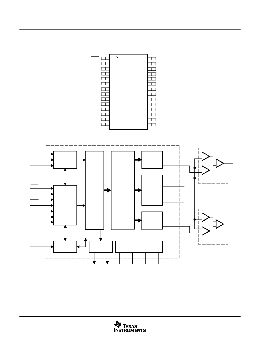
pin assignments
1
2
3
4
5
6
7
8
9
10
11
12
13
14
28
27
26
25
24
23
22
21
20
19
18
17
16
15
RST
ZEROL
ZEROR
LRCK
DATA
BCK
SCKI
DGND
V
DD
DEMP0
DEMP1
FMT0
FMT1
FMT2
V
CC
3
AGND2
I
OUT
L≠
I
OUT
L+
V
CC
2
V
CC
1
V
COM
3
I
REF
V
COM
2
V
COM
1
AGND1
I
OUT
R+
I
OUT
R≠
MUTE
SSOP PACKAGE
(TOP VIEW)
functional block diagram
System Clock
Manager
Serial
Input
I/F
Function
Control
I/F
System Clock
Zero Detect
Power Supply
ZEROL
LRCK
DATA
BCK
RST
MUTE
FMT0
FMT2
FMT1
DEMP0
DEMP1
SCKI
Digital
Filter
Advanced
Segment
DAC
Modulator
IOUTL+
Current
Segment
DAC
IOUTL≠
IOUTR≠
Current
Segment
DAC
IOUTR+
IREF
Bias
and
Vref
VCOM1
VCOM3
VCOM2
AGND2
V
DD
DGND
V
CC
1
V
CC
2
V
CC
3
AGND1
I/V and Filter
I/V and Filter
ZEROR
PCM1730
SLES021 ≠ NOVEMBER 2001
3
www.ti.com
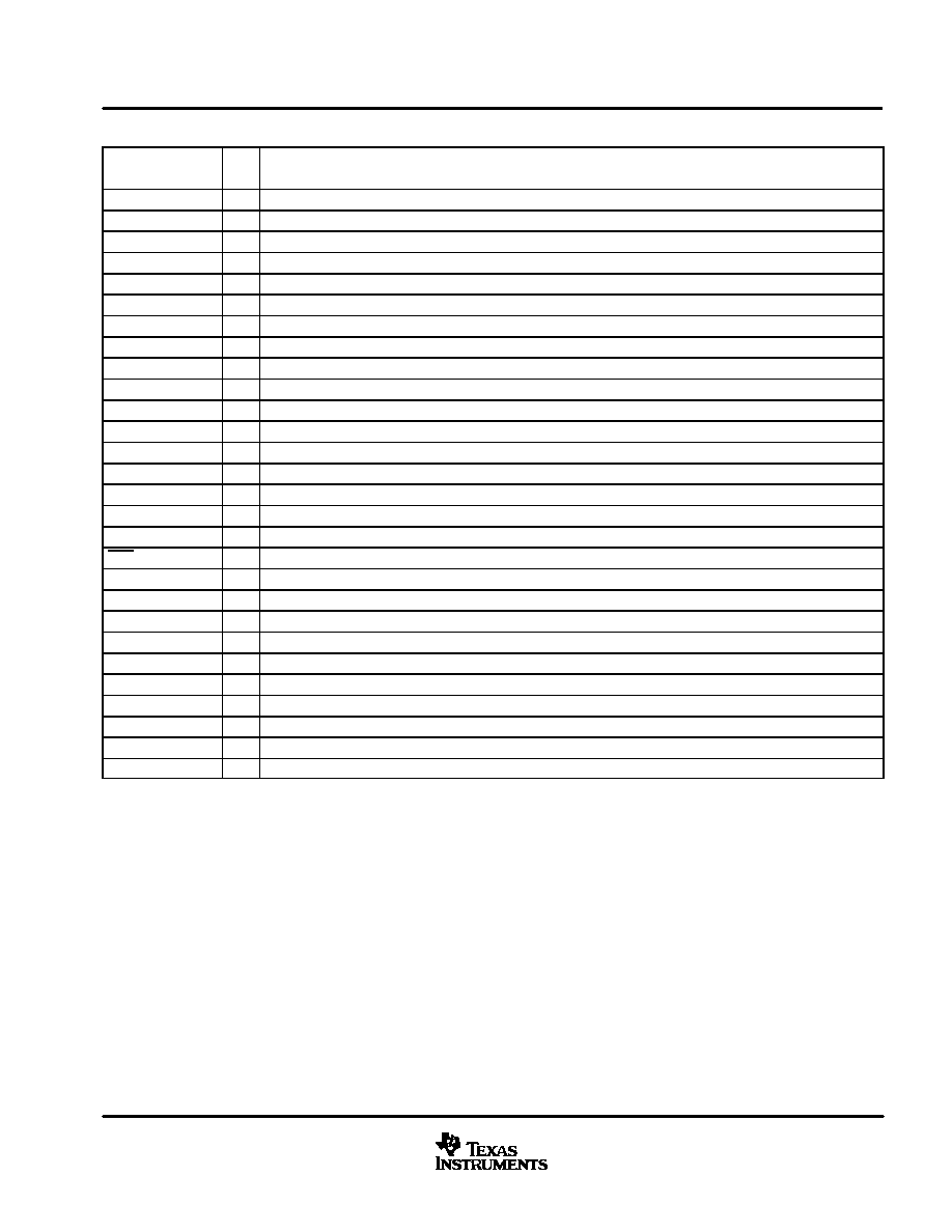
Terminal Functions
TERMINAL
I/O
DESCRIPTION
NAME
PIN
I/O
DESCRIPTION
AGND1
18
≠
Analog ground
AGND2
27
≠
Analog ground
BCK
6
I
Bit clock input
DATA
5
I
Serial audio data input
DEMP0
10
I
De-emphasis control
DEMP1
11
I
De-emphasis control
DGND
8
≠
Digital ground
FMT0
12
I
Audio data format select
FMT1
13
I
Audio data format select
FMT2
14
I
Audio data format select
IOUTL
≠
26
O
L-channel analog current output ≠
IOUTL+
25
O
L-channel analog current output +
IOUTR
≠
16
O
R-channel analog current output ≠
IOUTR+
17
O
R-channel analog current output +
IREF
21
≠
Output current reference bias pin. Connect a 16-k
resistor to GND.
LRCK
4
I
Left and right clock (fS)
MUTE
15
I
Analog output mute control
RST
1
I
Reset
SCKI
7
I
System clock input
VCC1
23
≠
Analog supply, 5 V
VCC2
24
≠
Analog supply, 5 V
VCC3
28
≠
Analog power supply, 5 V
VCOM1
19
≠
Internal bias decoupling pin
VCOM2
20
≠
Common voltage for I/V
VCOM3
22
≠
Internal bias decoupling pin
VDD
9
≠
Digital supply, 3.3 V
ZEROL
2
O
Zero flag for L-channel
ZEROR
3
O
Zero flag for R-channel
Schmitt-trigger input, 5-V tolerant
Schmitt-trigger input with internal pulldown, 5-V tolerant
PCM1730
SLES021 ≠ NOVEMBER 2001
4
www.ti.com
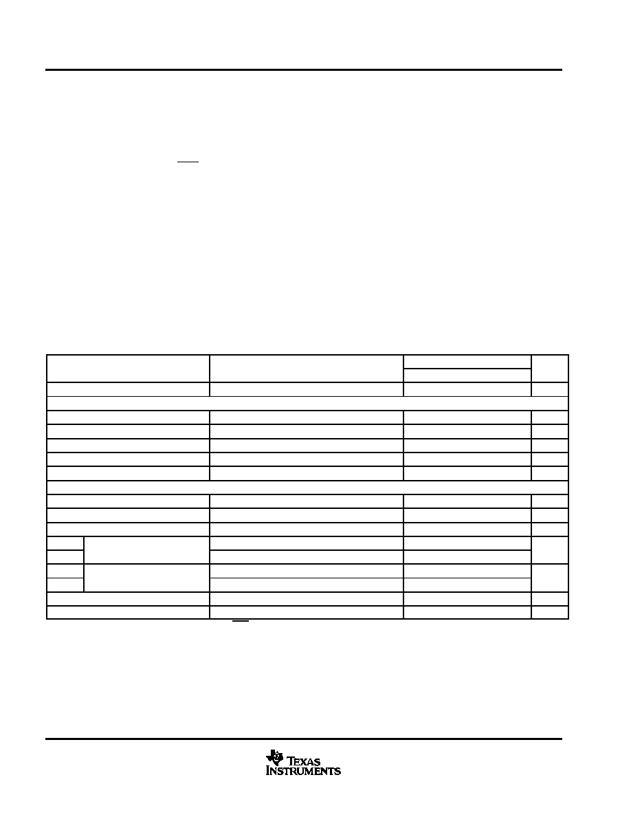
absolute maximum ratings over operating free-air temperature (unless otherwise noted)
Supply voltage: V
CC
1, V
CC
2, V
CC
3
6.5 V
. . . . . . . . . . . . . . . . . . . . . . . . . . . . . . . . . . . . . . . . . . . . . . . . . . . . . . . . . . . . . .
Supply voltage: V
DD
4 V
. . . . . . . . . . . . . . . . . . . . . . . . . . . . . . . . . . . . . . . . . . . . . . . . . . . . . . . . . . . . . . . . . . . . . . . . . . . . .
Supply voltage differences: V
CC
1, V
CC
2, and V
CC
3
±
0.1 V
. . . . . . . . . . . . . . . . . . . . . . . . . . . . . . . . . . . . . . . . . . . . . . .
Ground voltage differences: AGND1, AGND2, and DGND
±
0.1 V
. . . . . . . . . . . . . . . . . . . . . . . . . . . . . . . . . . . . . . . . . .
Digital input voltage: LRCK, DATA, BCK, SCKI, DEMP0, DEMP1, FMT0, FMT1,
FMT2, RST, and MUTE
≠0.3 V to 6.5 V
. . . . . . . . . . . . . . . . . . . . . . . . . . . . . . . . . . . . . . . . . . . . . .
Digital input voltage: ZEROL, ZEROR
≠
0.3 V to (V
DD
+ 0.3 V)
. . . . . . . . . . . . . . . . . . . . . . . . . . . . . . . . . . . . . . . . . . . .
Analog input voltage:
≠
0.3 V to (V
CC
+ 0.3 V)
. . . . . . . . . . . . . . . . . . . . . . . . . . . . . . . . . . . . . . . . . . . . . . . . . . . . . . . . . . .
Input current (any pins except supplies)
±
10 mA
. . . . . . . . . . . . . . . . . . . . . . . . . . . . . . . . . . . . . . . . . . . . . . . . . . . . . . . .
Ambient temperature under bias, T
A
≠
40
∞
C to 125
∞
C
. . . . . . . . . . . . . . . . . . . . . . . . . . . . . . . . . . . . . . . . . . . . . . . . . . . .
Storage temperature, T
stg
≠
55
∞
C to 150
∞
C
. . . . . . . . . . . . . . . . . . . . . . . . . . . . . . . . . . . . . . . . . . . . . . . . . . . . . . . . . . . . . .
Junction temperature, T
J
150
∞
C
. . . . . . . . . . . . . . . . . . . . . . . . . . . . . . . . . . . . . . . . . . . . . . . . . . . . . . . . . . . . . . . . . . . . . .
Lead temperature (soldering)
260
∞
C, 5 s
. . . . . . . . . . . . . . . . . . . . . . . . . . . . . . . . . . . . . . . . . . . . . . . . . . . . . . . . . . . . . . . .
Package temperature (IR reflow, peak)
235
∞
C, 10 s
. . . . . . . . . . . . . . . . . . . . . . . . . . . . . . . . . . . . . . . . . . . . . . . . . . . . . .
Stresses beyond those listed under "absolute maximum ratings" may cause permanent damage to the device. These are stress ratings only, and
functional operation of the device at these or any other conditions beyond those indicated under "recommended operating conditions" is not
implied. Exposure to absolute-maximum-rated conditions for extended periods may affect device reliability.
electrical characteristics, all specifications at T
A
= 25
∞
C, V
CC
= 5 V, V
DD
= 3.3 V, f
S
= 44.1 kHz, system
clock = 256 f
S
and 24-bit data (unless otherwise noted)
PARAMETER
TEST CONDITIONS
PCM1730E
UNIT
PARAMETER
TEST CONDITIONS
MIN
TYP
MAX
UNIT
RESOLUTION
24
Bits
DATA FORMAT
Audio data interface format
Standard, I2S, left justified
Audio data bit length
16, 20, 24-bits selectable
Audio data format
MSB first, 2's complement
fS
Sampling frequency
10
200
kHz
System clock frequency
128, 192, 256, 384, 512, 768 fS
DIGITAL INPUT/OUTPUT
Logic family
TTL compatible
VIH
High-level input logic level
2
VDC
VIL
Low-level input logic level
0.8
VDC
IIH
Input logic current (see Note 1)
VIN = VDD
10
A
IIL
Input logic current (see Note 1)
VIN = 0 V
≠10
µ
A
IIH
Input logic current (see Note 2)
VIN = VDD
65
100
A
IIL
Input logic current (see Note 2)
VIN = 0 V
≠10
µ
A
VOH
High-level output logic level
IOH = ≠2 mA
2.4
VDC
VOL
Low-level output logic level
IOL = 2 mA
1
VDC
NOTES:
1. Pins 1, 4, 5, 6, 7, 12, 13, 14, and 15: RST, LRCK, DATA, BCK, SCKI, FMT0, FMT1, FMT2, and MUTE
2. Pins 10 and 11: DEMP0, DEMP1

PCM1730
SLES021 ≠ NOVEMBER 2001
5
www.ti.com
electrical characteristics, all specifications at T
A
= 25
∞
C, V
CC
= 5 V, V
DD
= 3.3 V, f
S
= 44.1 kHz, system
clock = 256 f
S
and 24-bit data (unless otherwise noted) (continued)
PARAMETER
TEST CONDITIONS
PCM1730E
UNIT
PARAMETER
TEST CONDITIONS
MIN
TYP
MAX
UNIT
DYNAMIC PERFORMANCE (see Note 3)
T t l h
i di t ti
l
fS = 44.1 kHz
0.0004%
0.008%
THD+N
Total harmonic distortion plus
noise
VOUT = 0 dB
fS = 96 kHz
0.0006%
THD+N
noise
VOUT 0 dB
fS = 192 kHz
0.0012%
EIAJ, A-weighted, fS = 44.1 kHz
114
117
Dynamic range
EIAJ, A-weighted, fS = 96 kHz
117
dB
Dynamic range
EIAJ, A-weighted, fS = 192 kHz
117
dB
EIAJ, A-weighted, fS = 44.1 kHz
114
117
Signal-to-noise ratio
EIAJ, A-weighted, fS = 96 kHz
117
dB
Signal to noise ratio
EIAJ, A-weighted, fS = 192 kHz
117
dB
fS = 44.1 kHz
110
115
Channel separation
fS = 96 kHz
113
dB
Channel se aration
fS = 192 kHz
111
dB
Level linearity error
VOUT = ≠110 dB
±
1
dB
DC ACCURACY
VCOM2 voltage
2.45
V
VCOM2 output current
Delta VCOM2 < 5%
100
µ
A
Gain error
±
2
%/FSR
Gain mismatch, channel-to-
channel
±
0.5
%/FSR
Bipolar zero error
At BPZ
±
0.5
%/FSR
ANALOG OUTPUT
Output current
Full scale (≠0 dB)
±
2.48
mAp-p
Center current
BPZ input
0
mAp-p
DIGITAL FILTER PERFORMANCE--FILTER CHARACTERISTICS
Pass band
±
0.002 dB
0.454 fS
Pass band
≠3 dB
0.49 fS
Stop band
0.546 fS
Pass-band ripple
≠75
±
0.002
dB
Stop band attenuation
Stop band = 0.546 fS
dB
Stop-band attenuation
Stop band = 0.567 fS
≠82
dB
Delay time
29/fS
s
De-emphasis error
±
0.1
dB
NOTE 3: Analog performance specifications are measured by audio precision II under averaging mode. At 44.1-kHz operation, measurement
bandwidth is limited to 20 kHz. At 96-kHz and 192-kHz operation, measurement bandwidth is limited to 40 kHz.