 | –≠–ª–µ–∫—Ç—Ä–æ–Ω–Ω—ã–π –∫–æ–º–ø–æ–Ω–µ–Ω—Ç: PCM1780 | –°–∫–∞—á–∞—Ç—å:  PDF PDF  ZIP ZIP |
Burr Brown Products
from Texas Instruments
FEATURES
APPLICATIONS
DESCRIPTION
PCM1780, PCM1781, PCM1782
SLES132A ≠ MARCH 2005 ≠ REVISED APRIL 2005
24-Bit, 192-kHz Sampling, Enhanced Multilevel, Delta-Sigma,
Audio Digital-to-Analog Converter
∑
A/V Receivers
∑
24-Bit Resolution
∑
DVD Movie Players
∑
Analog Performance (V
CC
= 5 V):
∑
DVD Add-On Cards For High-End PCs
≠ Dynamic Range: 106 dB
∑
DVD Audio Players
≠ SNR: 106 dB, Typical
∑
HDTV Receivers
≠ THD+N: 0.002%, Typical
∑
Car Audio Systems
≠ Full-Scale Output: 3.9 Vp-p, Typical
∑
Other Applications Requiring 24-Bit Audio
∑
4◊/8◊ Oversampling Digital Filter:
≠ Stop-Band Attenuation: ≠50 dB
≠ Pass-Band Ripple: ±0.04 dB
The PCM1780/81/82 is a CMOS, monolithic, inte-
∑
Sampling Frequency: 5 kHz to 200 kHz
grated circuit, which includes stereo digital-to-analog
converters and support circuitry in a small 16-lead
∑
System Clock: 128 f
S
, 192 f
S
, 256 f
S
, 384 f
S
,
SSOP package. The data converters use TI's en-
512 f
S
, 768 f
S
, 1152 f
S
With Autodetect
hanced multilevel delta-sigma architecture to achieve
∑
Software Control (PCM1780, PCM1782):
excellent dynamic performance and improved toler-
≠ Accepts 16-, 18-, 20-, and 24-Bit Audio Data
ance to clock jitter. The PCM1780/81/82 accepts
industry standard audio data formats with 16- to
≠ Formats: Right-Justified, I
2
S, and
24-bit data, providing easy interfacing to audio DSP
Left-Justified
and decoder chips. Sampling rates up to 200 kHz are
≠ Digital Attenuation: Mode Selectable
supported. The PCM1780/82 provides a full set of
∑
0 dB to ≠63 dB, 0.5 dB/step
user-programmable functions through a three-wire
serial control port, which supports register write
∑
0 dB to ≠100 dB, 1 dB/step
functions. The PCM1781 provides a subset of
≠ Digital De-Emphasis
user-programmable functions through four control
≠ Digital Filter Rolloff: Sharp or Slow
pins.
≠ Soft Mute
The PCM1780 is pin-compatible with the PCM1680
≠ Zero Flags for Each Output
(8-channel DAC).
≠ Open-Drain Output Zero Flag (PCM1782)
∑
Hardware Control (PCM1781):
≠ I
2
S and 16-Bit Word, Right-Justified
≠ Digital De-Emphasis
≠ Soft Mute
≠ Zero Flag for L-, R-Channel Common Output
∑
Power Supply: 5-V Single Supply
∑
Small, 16-Lead SSOP Package (150 mil)
∑
Pin-Compatible with PCM1680
Please be aware that an important notice concerning availability, standard warranty, and use in critical applications of Texas
Instruments semiconductor products and disclaimers thereto appears at the end of this data sheet.
System Two, Audio Precision are trademarks of Audio Precision, Inc.
All trademarks are the property of their respective owners.
PRODUCTION DATA information is current as of publication date.
Copyright © 2005, Texas Instruments Incorporated
Products conform to specifications per the terms of the Texas
Instruments standard warranty. Production processing does not
necessarily include testing of all parameters.

www.ti.com
ABSOLUTE MAXIMUM RATINGS
RECOMMENDED OPERATING CONDITIONS
ELECTRICAL CHARACTERISTICS
PCM1780, PCM1781, PCM1782
SLES132A ≠ MARCH 2005 ≠ REVISED APRIL 2005
This integrated circuit can be damaged by ESD. Texas Instruments recommends that all integrated
circuits be handled with appropriate precautions. Failure to observe proper handling and installation
procedures can cause damage. ESD damage can range from subtle performance degradation to
complete device failure. Precision integrated circuits may be more susceptible to damage because very
small parametric changes could cause the device not to meet its published specifications.
over operating free-air temperature range (unless otherwise noted)
(1)
PCM1780, PCM1781, PCM1782
Supply voltage
V
CC
≠0.3 V to 6.5 V
Input voltage
≠0.3 V to V
CC
+ 0.3 V, < 6.5 V
Input current (any pins except supplies)
±10 mA
Ambient temperature under bias
≠ 40∞C to 125∞C
Storage temperature
≠ 55∞C to 150∞C
Junction temperature
150∞C
Lead temperature (soldering)
260∞C, 5 s
Package temperature (IR reflow, peak)
260∞C
(1)
Stresses beyond those listed under "absolute maximum ratings" may cause permanent damage to the device. These are stress ratings
only, and functional operation of the device at these or any other conditions beyond those indicated under "recommended operating
conditions" is not implied. Exposure to absolute-maximum-rated conditions for extended periods may affect device reliability.
over operating free-air temperature range
MIN
NOM
MAX
UNIT
Digital and analog supply voltage, V
CC
4.5
5
5.5
V
Digital input logic family
TTL
System clock
8.192
36.864
MHz
Digital input clock frequency
Sampling clock
32
192
kHz
Analog output load resistance
5
k
Analog output load capacitance
50
pF
Digital output load capacitance
20
pF
Operating free-air temperature, T
A
≠25
85
∞C
All specifications at T
A
= 25∞C, V
CC
= 5 V, f
S
= 48 kHz, system clock = 512 f
S
, and 24-bit data (unless otherwise noted)
PARAMETER
TEST CONDITIONS
MIN
TYP
MAX
UNIT
Resolution
24
Bits
DATA FORMAT
PCM1780,
Right-justified, I
2
S,
PCM1782
left-justified
Audio data interface format
PCM1781
I
2
S, right-justified
PCM1780,
16-, 18-, 20-, 24-bit
PCM1782
selectable
Audio data bit length
16≠24-bit I
2
S, 16-bit
PCM1781
right-justified
Audio data format
MSB-first, 2s complement
f
S
Sampling frequency
5
200
kHz
128 f
S
, 192 f
S
, 256 f
S
, 384 f
S
,
System clock frequency
512 f
S
, 768 f
S
, 1152 f
S
2
www.ti.com
PCM1780, PCM1781, PCM1782
SLES132A ≠ MARCH 2005 ≠ REVISED APRIL 2005
ELECTRICAL CHARACTERISTICS (continued)
All specifications at T
A
= 25∞C, V
CC
= 5 V, f
S
= 48 kHz, system clock = 512 f
S
, and 24-bit data (unless otherwise noted)
PARAMETER
TEST CONDITIONS
MIN
TYP
MAX
UNIT
DIGITAL INPUT/OUTPUT
Logic family
TTL compatible
V
IH
2
Input logic level
Vdc
V
IL
0.8
I
IH
(1)
V
IN
= V
CC
10
I
IL
(1)
V
IN
= 0 V
≠10
Input logic current
µ
A
I
IH
(2)
V
IN
= V
CC
65
100
I
IL
(2)
V
IN
= 0 V
≠10
V
OH
(3)
I
OH
= ≠1 mA
2.4
Output logic level
Vdc
V
OL
(4)
I
OL
= 1 mA
0.4
DYNAMIC PERFORMANCE
(5)
V
OUT
= 0 dB, f
S
= 48 kHz
0.002%
0.006%
V
OUT
= 0 dB, f
S
= 96 kHz, system
0.003%
THD+N
Total harmonic distortion + noise
clock = 256 f
S
V
OUT
= 0 dB, f
S
= 192 kHz, system
0.004%
clock = 128 f
S
EIAJ, A-weighted, f
S
= 48 kHz
100
106
A-weighted, f
S
= 96 kHz, system
104
Dynamic range
clock = 256 f
S
dB
A-weighted, f
S
= 192 kHz, system
102
clock = 128 f
S
EIAJ, A-weighted, f
S
= 48 kHz
100
106
A-weighted, f
S
= 96 kHz, system
104
SNR
Signal-to-noise ratio
clock = 256 f
S
dB
A-weighted, f
S
= 192 kHz, system
102
clock = 128 f
S
f
S
= 48 kHz
97
103
Channel separation
f
S
= 96 kHz, system clock = 256 f
S
101
dB
f
S
= 192 kHz, system clock = 128 f
S
100
DC ACCURACY
% of
Gain error
±1
±6
FSR
% of
Gain mismatch, channel-to-channel
±1
±6
FSR
Bipolar zero error
V
OUT
= 49% of V
CC
at BPZ input
±30
±80
mV
ANALOG OUTPUT
Output voltage
Full scale (≠0 dB)
0.78 V
CC
Vp-p
Bipolar zero voltage
0.49 V
CC
Vdc
Load impedance
AC-coupled load
5
k
DIGITAL FILTER PERFORMANCE
Filter Characteristics (Sharp Rolloff)
Pass band
±0.04 dB
0.454 f
S
Stop band
0.546 f
S
Pass-band ripple
0.04
dB
Stop-band attenuation
Stop band = 0.546 f
S
≠50
dB
(1)
Pins 5, 6, 7, 8: SCK, DATA, BCK, LRCK
(2)
Pins 2, 3, 4: MS, MC, MD (PCM1780/PCM1782). Pins 1, 2, 3, 4: FMT, DEMP0, DEMP1, MUTE (PCM1781)
(3)
Pins 1, 16: ZEROL, ZEROR (PCM1780). Pin 16: ZEROA (PCM1781)
(4)
Pins 1, 16: ZEROL, ZEROR (PCM1780/PCM1782). Pin 16: ZEROA (PCM1781)
(5)
Analog performance specifications are measured using the System TwoTM Cascade audio measurement system by Audio PrecisionTM.
3
www.ti.com
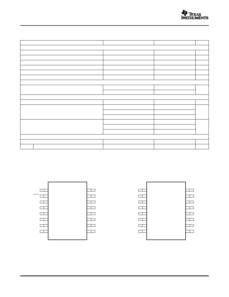
DEVICE INFORMATION
PIN ASSIGNMENTS
ZEROR/ZEROA
V
OUT
L
V
OUT
R
V
COM
AGND
V
CC
NC
NC
16
15
14
13
12
11
10
9
ZEROL/NA
MS
MC
MD
SCK
DATA
BCK
LRCK
PCM1780/PCM1782
(TOP VIEW)
1
2
3
4
5
6
7
8
ZEROA
V
OUT
L
V
OUT
R
V
COM
AGND
V
CC
NC
TEST
16
15
14
13
12
11
10
9
FMT
DEMP0
DEMP1
MUTE
SCK
DATA
BCK
LRCK
PCM1781
(TOP VIEW)
1
2
3
4
5
6
7
8
P0014-01
PCM1780, PCM1781, PCM1782
SLES132A ≠ MARCH 2005 ≠ REVISED APRIL 2005
ELECTRICAL CHARACTERISTICS (continued)
All specifications at T
A
= 25∞C, V
CC
= 5 V, f
S
= 48 kHz, system clock = 512 f
S
, and 24-bit data (unless otherwise noted)
PARAMETER
TEST CONDITIONS
MIN
TYP
MAX
UNIT
Filter Characteristics (Slow Rolloff, PCM1780/PCM1782)
Pass band
±0.5 dB
0.198 f
S
Stop band
0.884 f
S
Pass-band ripple
±0.5
dB
Stop-band attenuation
Stop band = 0.884 f
S
≠35
dB
Delay time
20/f
S
s
De-emphasis error
±0.1
dB
ANALOG FILTER PERFORMANCE
at 20 kHz
≠0.02
Frequency response
dB
at 44 kHz
≠0.07
POWER SUPPLY REQUIREMENTS
V
CC
Voltage range
4.5
5
5.5
Vdc
f
S
= 48 kHz
25
40
I
CC
Supply current
f
S
= 96 kHz, system clock = 256 f
S
30
mA
f
S
= 192 kHz, system clock = 128 f
S
30
f
S
= 48 kHz
125
200
Power dissipation
f
S
= 96 kHz, system clock = 256 f
S
150
mW
f
S
= 192 kHz, system clock = 128 f
S
150
TEMPERATURE RANGE
T
A
Operation temperature
≠25
85
∞C
JA
Thermal resistance
115
∞C/W
4
www.ti.com
PCM1780, PCM1781, PCM1782
SLES132A ≠ MARCH 2005 ≠ REVISED APRIL 2005
DEVICE INFORMATION (continued)
TERMINAL FUNCTIONS--PCM1780/PCM1782
TERMINAL
I/O
DESCRIPTION
NAME
NO.
AGND
12
≠
Ground
BCK
7
I
Audio data bit clock input
(1)
DATA
6
I
Audio data digital input
(1)
LRCK
8
I
Audio data left and right clock input
(1)
MC
3
I
Mode control clock input
(1) (2)
MD
4
I
Mode control data input
(1) (2)
MS
2
I
Mode control select input
(1) (2)
NC
9, 10
≠
No connection
SCK
5
I
System clock input
(1)
V
CC
11
≠
Power supply, 5-V
V
COM
13
≠
Common voltage decoupling
V
OUT
L
15
O
Analog output for L-channel
V
OUT
R
14
O
Analog output for R-channel
ZEROL/NA
1
O
Zero flag output for L-channel / No assign
(3)
ZEROR/ZEROA
16
O
Zero flag output for R-channel / Zero flag output for L- and R-channels
(3)
(1)
Schmitt-trigger input
(2)
Pulldown
(3)
Open-drain output (PCM1782)
TERMINAL FUNCTIONS--PCM1781
TERMINAL
I/O
DESCRIPTION
NAME
NO.
AGND
12
≠
Ground
BCK
7
I
Audio data bit clock input
(1)
DATA
6
I
Audio data digital input
(1)
DEMP0
2
I
De-emphasis control
(1) (2)
DEMP1
3
I
De-emphasis control
(1) (2)
FMT
1
I
Data format select
(1) (2)
LRCK
8
I
Audio data left and right clock input
(1)
MUTE
4
I
Soft mute control
(1) (2)
NC
10
≠
No connection
SCK
5
I
System clock input
(1)
TEST
9
≠
Test pin for factory use. Must be LOW or open
(1) (2)
V
CC
11
≠
Power supply, 5-V
V
COM
13
≠
Common voltage decoupling
V
OUT
L
15
O
Analog output for L-channel
V
OUT
R
14
O
Analog output for R-channel
ZEROA
16
O
Zero flag output for L- and R-channels
(1)
Schmitt-trigger input
(2)
Pulldown
5