Äîêóìåíòàöèÿ è îïèñàíèÿ www.docs.chipfind.ru
PCM1791A
SLES071A - MARCH 2003 - REVISED JANUARY 2004
24 BIT, 192 kHz SAMPLING, ADVANCED SEGMENT,
AUDIO STEREO DIGITAL TO ANALOG CONVERTER
FEATURES
D
24-Bit Resolution
D
Analog Performance:
- Dynamic Range: 113 dB
- THD+N: 0.001%
- Full-Scale Output: 2.1 V RMS (at Postamp)
D
Differential Voltage Output: 3.2 Vp-p
D
8
×
Oversampling Digital Filter:
- Stop-Band Attenuation: 82 dB
- Pass-Band Ripple:
±
0.002 dB
D
Sampling Frequency: 10 kHz to 200 kHz
D
System Clock: 128, 192, 256, 384, 512, or
768 f
S
With Autodetect
D
Accepts 16-, 20-, and 24-Bit Audio Data
D
PCM Data Formats: Standard, I
2
S, and
Left-Justified
D
DSD Format Interface Available
D
Optional Interface to External Digital Filter or
DSP Available
D
TDMCA or Serial Port (SPI/I
2
C)
D
User-Programmable Mode Controls:
- Digital Attenuation: 0 dB to 120 dB,
0.5 dB/Step
- Digital De-Emphasis
- Digital Filter Rolloff: Sharp or Slow
- Soft Mute
- Zero Flag for Each Output/PCM and DSD
Formats
D
Dual Supply Operation:
- 5-V Analog, 3.3-V Digital
D
5-V Tolerant Digital Inputs
D
Small 28-Lead SSOP Package, Lead-Free
Product
APPLICATIONS
D
A/V Receivers
D
SACD Players
D
DVD Players
D
HDTV Receivers
D
Car Audio Systems
D
Digital Multitrack Recorders
D
Other Applications Requiring 24-Bit Audio
DESCRIPTION
The PCM1791A is a monolithic CMOS integrated circuit
that includes stereo digital-to-analog converters and
support circuitry in a small 28-lead SSOP package. The
data converters use TI's advanced segment DAC
architecture to achieve excellent dynamic performance
and improved tolerance to clock jitter. The PCM1791A
provides balanced voltage outputs, allowing the user to
optimize analog performance externally. The PCM1791A
accepts PCM and DSD audio data formats, providing easy
interfacing to audio DSP and decoder chips. The
PCM1791A also accepts interface to external digital filter
devices (DF1704, DF1706, PMD200). Sampling rates up
to 200 kHz are supported. A full set of user-programmable
functions is accessible through an SPI or I
2
C serial control
port, which supports register write and readback functions.
The PCM1791A also supports the time-division-
multiplexed command and audio (TDMCA) data format.
This integrated circuit can be damaged by ESD. Texas Instruments recommends that all integrated circuits be handled with appropriate
precautions. Failure to observe proper handling and installation procedures can cause damage.
ESD damage can range from subtle performance degradation to complete device failure. Precision integrated circuits may be more susceptible to
damage because very small parametric changes could cause the device not to meet its published specifications.
PRODUCTION DATA information is current as of publication date. Products
conform to specifications per the terms of Texas Instruments standard warranty.
Production processing does not necessarily include testing of all parameters.
Please be aware that an important notice concerning availability, standard warranty, and use in critical applications of Texas Instruments
semiconductor products and disclaimers thereto appears at the end of this data sheet.
Burr Brown Products
from Texas Instruments
Copyright
2004, Texas Instruments Incorporated
PCM1791A
SLES071A - MARCH 2003 - REVISED JANUARY 2004
www.ti.com
2
ORDERING INFORMATION
PRODUCT
PACKAGE
PACKAGE CODE
OPERATION
TEMPERATURE
RANGE
PACKAGE
MARKING
ORDERING
NUMBER
TRANSPORT
MEDIA
PCM1791ADB
28-lead SSOP
28DB
-25
°
C to 85
°
C
PCM1791A
PCM1791ADB
Tube
PCM1791ADB
28-lead SSOP
28DB
-25
°
C to 85
°
C
PCM1791A
PCM1791ADBR
Tape and reel
ABSOLUTE MAXIMUM RATINGS
over operating free-air temperature range unless otherwise noted(1)
PCM1791A
Supply voltage
VCCF, VCCL, VCCC, VCCR
-0.3 V to 6.5 V
Supply voltage
VDD
-0.3 V to 4 V
Supply voltage differences: VCCF, VCCL, VCCC, VCCR
±
0.1 V
Ground voltage differences: AGNDF, AGNDL, AGNDC, AGNDR, DGND
±
0.1 V
Digital input voltage
LRCK, DATA, BCK, SCK, MS(2), MDI(2), MC, MUTE, RST, MSEL
0.3 V to 6.5 V
Digital input voltage
ZEROL, ZEROR, MDO, MS(3), MDI(3)
0.3 V to (VDD + 0.3 V) < 4 V
Analog input voltage
0.3 V to (VCC + 0.3 V) < 6.5 V
Input current (any pins except supplies)
±
10 mA
Ambient temperature under bias
40
°
C to 125
°
C
Storage temperature
55
°
C to 150
°
C
Junction temperature
150
°
C
Lead temperature (soldering)
260
°
C, 5 s
Package temperature (IR reflow, peak)
260
°
C
(1) Stresses beyond those listed under "absolute maximum ratings" may cause permanent damage to the device. These are stress ratings only, and
functional operation of the device at these or any other conditions beyond those indicated under "recommended operating conditions" is not
implied. Exposure to absolute-maximum-rated conditions for extended periods may affect device reliability.
(2) Input mode or I2C mode.
(3) Output mode except for I2C mode.
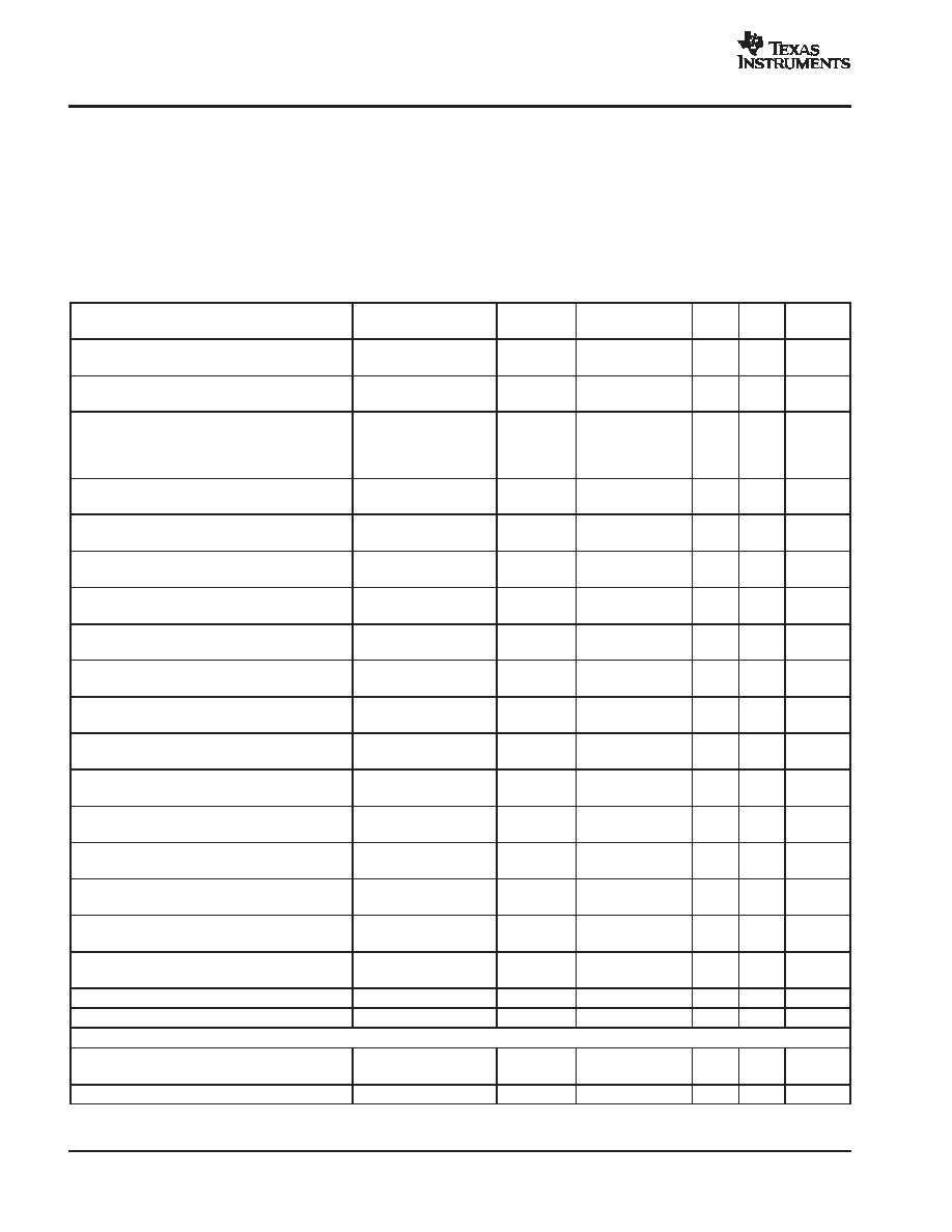
ELECTRICAL CHARACTERISTICS
all specifications at TA = 25
°
C, VCC = 5 V, VDD = 3.3 V, fS = 44.1 kHz, system clock = 256 fS, and 24-bit data, unless otherwise noted
PARAMETER
PCM1791ADB
UNIT
PARAMETER
MIN
TYP
MAX
UNIT
RESOLUTION
24
Bits
DATA FORMAT (PCM Mode)
Audio data interface format
Standard, I2S, left justified
Audio data bit length
16-, 20-, 24-bit selectable
Audio data format
MSB first, 2s complement
fS
Sampling frequency
10
200
kHz
System clock frequency
128, 192, 256, 384, 512, 768 fS
DATA FORMAT (DSD Mode)
Audio data interface format
DSD (Direct stream digital)
Audio data bit length
1 Bit
fS
Sampling frequency
2.8224
MHz
System clock frequency
2.8224
11.2896
MHz
PCM1791A
SLES071A - MARCH 2003 - REVISED JANUARY 2004
www.ti.com
3
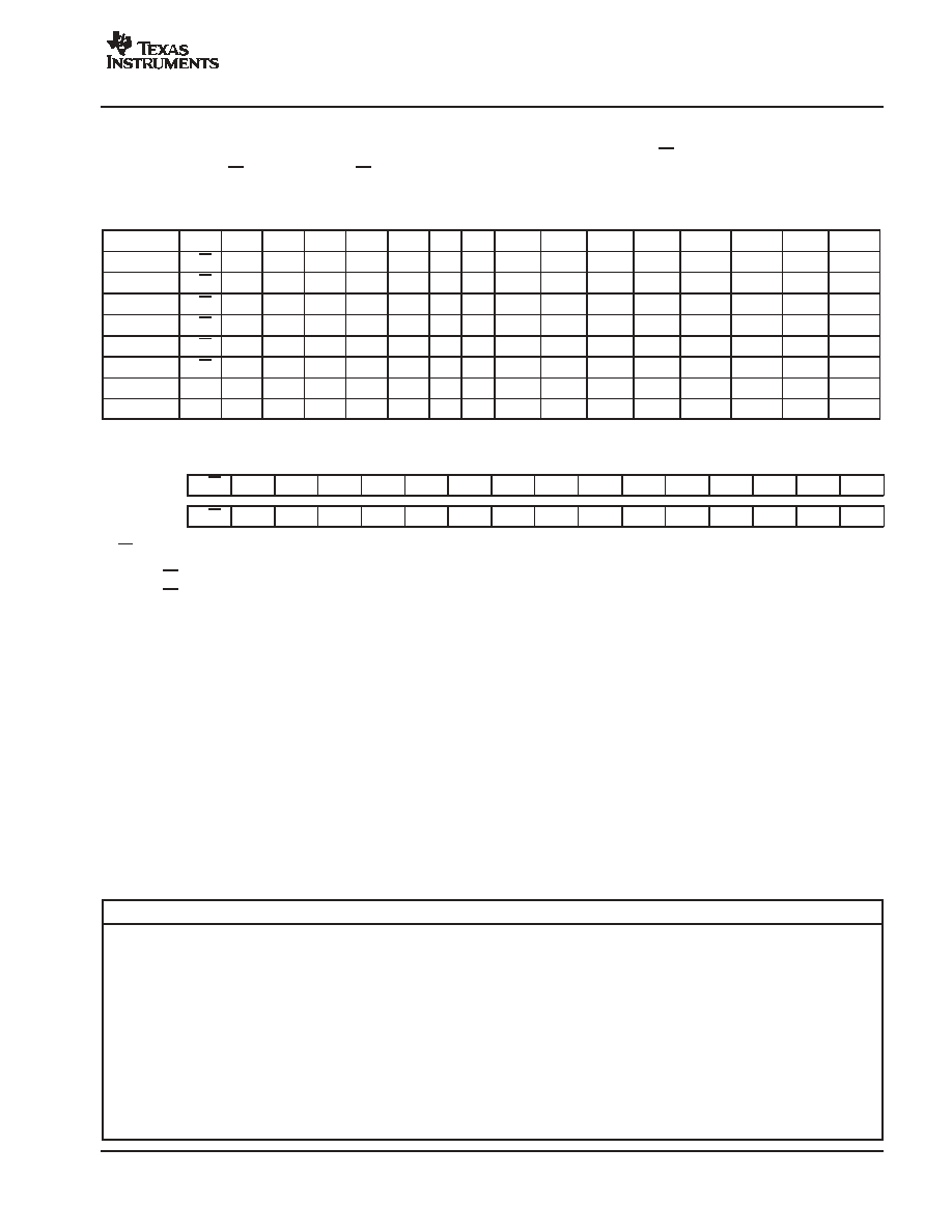
ELECTRICAL CHARACTERISTICS (Continued)
all specifications at TA = 25
°
C, VCC = 5 V, VDD = 3.3 V, fS = 44.1 kHz, system clock = 256 fS, and 24-bit data, unless otherwise noted
PARAMETER
TEST CONDITIONS
PCM1791ADB
UNIT
PARAMETER
TEST CONDITIONS
MIN
TYP
MAX
UNIT
DIGITAL INPUT/OUTPUT
Logic family
TTL compatible
VIH
Input logic level
2
VDC
VIL
Input logic level
0.8
VDC
IIH
Input logic current
VIN = VDD
10
A
IIL
Input logic current
VIN = 0 V
10
µ
A
VOH
Output logic level
IOH = 2 mA
2.4
VDC
VOL
Output logic level
IOL = 2 mA
0.4
VDC
IOHZ
High-impedance output logic current (1)
VOUT = VDD
10
A
IOLZ
High-impedance output logic current (1)
VOUT = 0 V
-10
µ
A
DYNAMIC PERFORMANCE (PCM MODE) (2)
fS = 44.1 kHz
0.001%
0.002%
THD+N at VOUT = 0 dB
fS = 96 kHz
0.0015%
THD+N at VOUT = 0 dB
fS = 192 kHz
0.003%
EIAJ, A-weighted, fS = 44.1 kHz
110
113
Dynamic range
EIAJ, A-weighted, fS = 96 kHz
113
dB
Dynamic range
EIAJ, A-weighted, fS = 192 kHz
113
dB
EIAJ, A-weighted, fS = 44.1 kHz
110
113
Signal-to-noise ratio
EIAJ, A-weighted, fS = 96 kHz
113
dB
Signal-to-noise ratio
EIAJ, A-weighted, fS = 192 kHz
113
dB
fS = 44.1 kHz
106
110
Channel separation
fS = 96 kHz
110
dB
Channel separation
fS = 192 kHz
109
dB
Level linearity error
VOUT = 120 dB
±
1
dB
DYNAMIC PERFORMANCE (DSD MODE) (2) (3)
THD+N at VOUT = 0 dB
2.1 V rms
0.001%
Dynamic range
60 dB, EIAJ, A-weighted
113
dB
Signal-to-noise ratio
EIAJ, A-weighted
113
dB
ANALOG OUTPUT
Gain error
8
±
3
8
% of FSR
Gain mismatch, channel-to-channel
3
±
0.5
3
% of FSR
Bipolar zero error
At BPZ
2
±
0.5
2
% of FSR
Differential output voltage (4)
Full scale (0 dB)
3.2
V p-p
Bipolar zero voltage (4)
At BPZ
1.4
V
Load impedance (4)
R1 = R2
1.7
k
(1) MDO pin
(2) Dynamic performance and DC accuracy are specified at the output of the postamplifier as shown in Figure 36. Analog performance specifications
are measured using the System Two
t
Cascade audio measurement system by Audio Precision
t
in the averaging mode. For all
sampling-frequency operations, measurement bandwidth is limited with a 20-kHz AES17 filter.
(3) Analog performance in the DSD mode is specified as the DSD modulation index of 100%. This is equivalent to PCM-mode performance at
44.1 kHz and 64 fS.
(4) These parameters are defined at the PCM1791A output pins. Load impedances, R1 and R2, are input resistors of the postamplifier. They are
defined as dc loads.
Audio Precision and System Two are trademarks of Audio Precision, Inc.
Other trademarks are the property of their respective owners.
PCM1791A
SLES071A - MARCH 2003 - REVISED JANUARY 2004
www.ti.com
4
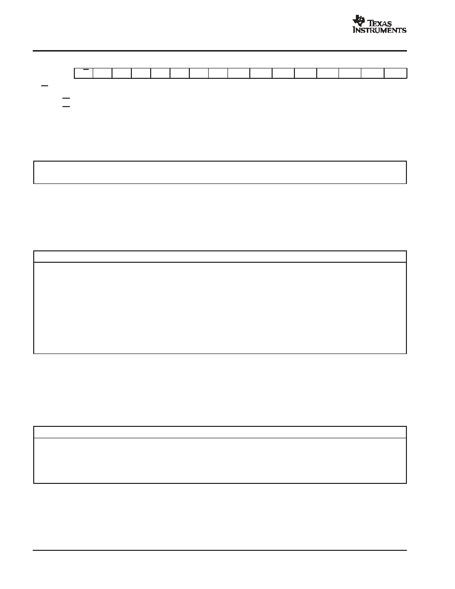
ELECTRICAL CHARACTERISTICS (Continued)
all specifications at TA = 25
°
C, VCC = 5 V, VDD = 3.3 V, fS = 44.1 kHz, system clock = 256 fS, and 24-bit data, unless otherwise noted
PARAMETER
TEST CONDITIONS
PCM1791ADB
UNIT
PARAMETER
TEST CONDITIONS
MIN
TYP
MAX
UNIT
DIGITAL FILTER PERFORMANCE
De-emphasis error
±
0.1
dB
FILTER CHARACTERISTICS-1: SHARP ROLL OFF
Pass band
±
0.002 dB
0.454 fS
Pass band
3 dB
0.49 fS
Stop band
0.546 fS
Pass-band ripple
±
0.002
dB
Stop-band attenuation
Stop band = 0.546 fS
75
dB
Stop-band attenuation
Stop band = 0.567 fS
-82
dB
Delay time
29/fS
s
FILTER CHARACTERISTICS-2: SLOW ROLL OFF
Pass band
±
0.04 dB
0.274 fS
Pass band
3 dB
0.454 fS
Stop band
0.732 fS
Pass-band ripple
±
0.002
dB
Stop-band attenuation
Stop band = 0.732 fS
82
dB
Delay time
29/fS
s
POWER SUPPLY REQUIREMENTS
VDD
Voltage range
3
3.3
3.6
VDC
VCC
Voltage range
4.5
5
5.5
VDC
(1)
fS = 44.1 kHz
6.5
8
IDD
Supply current (1)
fS = 96 kHz
13.5
mA
IDD
Supply current (1)
fS = 192 kHz
28
mA
(1)
fS = 44.1 kHz
14
16
ICC
Supply current (1)
fS = 96 kHz
15
mA
ICC
Supply current (1)
fS = 192 kHz
16
mA
(1)
fS = 44.1 kHz
90
110
Power dissipation (1)
fS = 96 kHz
120
mW
Power dissipation (1)
fS = 192 kHz
170
mW
TEMPERATURE RANGE
Operation temperature
25
85
°
C
JA
Thermal resistance
28-pin SSOP
100
°
C/W
(1) Input is BPZ data.
PCM1791A
SLES071A - MARCH 2003 - REVISED JANUARY 2004
www.ti.com
5
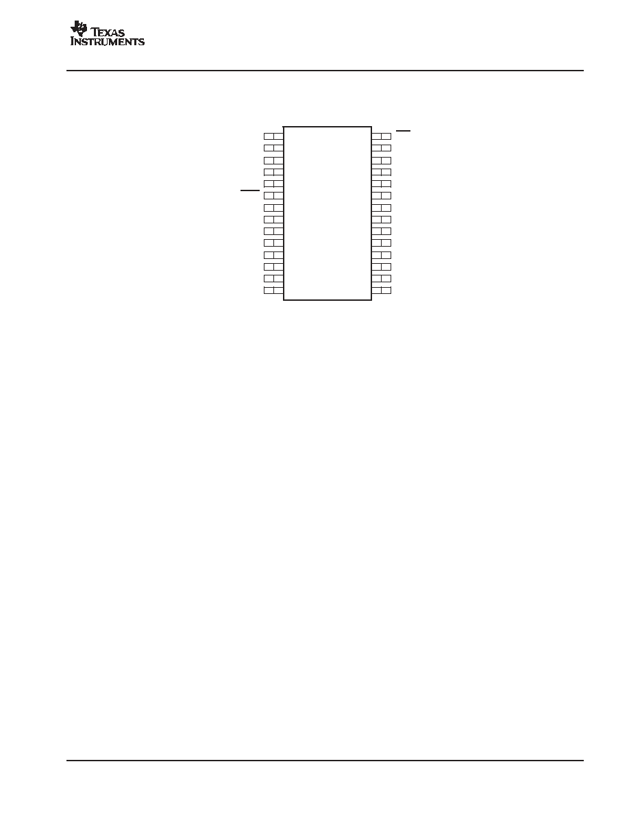
PIN ASSIGNMENTS
1
2
3
4
5
6
7
8
9
10
11
12
13
14
28
27
26
25
24
23
22
21
20
19
18
17
16
15
LRCK
BCK
DATA
MUTE
SCK
RST
V
DD
DGND
AGNDF
V
CC
R
AGNDR
V
OUT
R-
V
OUT
R+
V
COM
MS
MC
MDI
MDO
MSEL
ZEROL
ZEROR
V
CC
F
V
CC
L
AGNDL
V
OUT
L-
V
OUT
L+
AGNDC
V
CC
C
PCM1791A
(TOP VIEW)
PCM1791A
SLES071A - MARCH 2003 - REVISED JANUARY 2004
www.ti.com
6
Terminal Functions
TERMINAL
I/O
DESCRIPTIONS
NAME
PIN
I/O
DESCRIPTIONS
AGNDC
16
-
Analog ground (internal bias and current DAC)
AGNDF
9
-
Analog ground (DACFF)
AGNDL
19
-
Analog ground (L-channel I/V)
AGNDR
11
-
Analog ground (R-channel I/V)
BCK
2
I
Bit clock input (1)
DATA
3
I
Serial audio data input (1)
DGND
8
-
Digital ground
LRCK
1
I
Left and right clock (fS) input (1)
MC
27
I
Mode control clock input (1)
MDI
26
I/O
Mode control data input (2)
MDO
25
O
Mode control readback data output (3)
MS
28
I/O
Mode control chip select input (4)
MSEL
24
I
I2C/SPI select (1)
MUTE
4
I
Analog output mute control (1)
RST
6
I
Reset (1)
SCK
5
I
System clock input (1)
VCCC
15
-
Analog power supply (internal bias and current DAC), 5 V
VCCF
21
-
Analog power supply (DACFF), 5 V
VCCL
20
-
Analog power supply (L-channel I/V), 5 V
VCCR
10
-
Analog power supply (R-channel I/V), 5 V
VCOM
14
-
Internal bias decoupling pin
VDD
7
-
Digital power supply, 3.3 V
VOUTL+
17
O
L-channel analog voltage output +
VOUTL
18
O
L-channel analog voltage output
VOUTR+
13
O
R-channel analog voltage output +
VOUTR
12
O
R-channel analog voltage output
ZEROL
23
O
Zero flag for L-channel
ZEROR
22
O
Zero flag for R-channel
(1) Schmitt-trigger input, 5-V tolerant
(2) Schmitt-trigger input and output. 5-V tolerant input. In I2C mode, this pin becomes an open-drain 3-state output; otherwise, this pin is a CMOS
output.
(3) 3-state output
(4) Schmitt-trigger input and output. 5-V tolerant input and CMOS output
PCM1791A
SLES071A - MARCH 2003 - REVISED JANUARY 2004
www.ti.com
7
FUNCTIONAL BLOCK DIAGRAM
Power Supply
RST
SCK
Advanced
Segment
DAC
Modulator
VOUTL+
VOUTL-
Bias
and
Vref
V
CC
F
V
DD
AGNDR
V
CC
R
AGNDL
AGNDF
D/S and Filter
8
Oversampling
Digital
Filter
and
Function
Control
Audio
Data Input
I/F
LRCK
BCK
DATA
MDO
MDI
MC
MS
AGNDC
V
CC
C
DGND
Current
Segment
DAC
and
I/V Buffer
VCOM
Function
Control
I/F
Zero
Detect
ZEROL
ZEROR
System
Clock
Manager
MSEL
MUTE
V
CC
L
VOUTR-
VOUTR+
D/S and Filter
Current
Segment
DAC
and
I/V Buffer
PCM1791A
SLES071A - MARCH 2003 - REVISED JANUARY 2004
www.ti.com
8
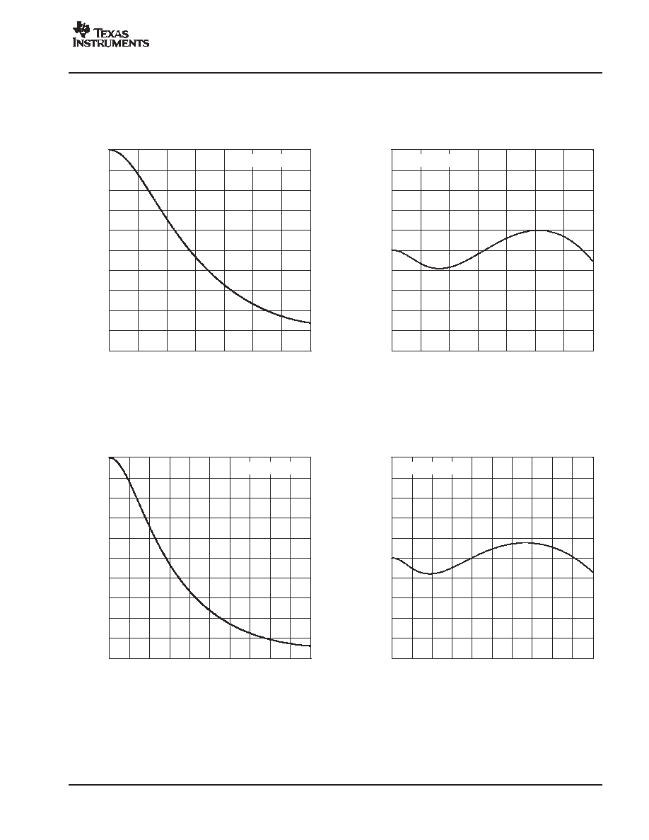
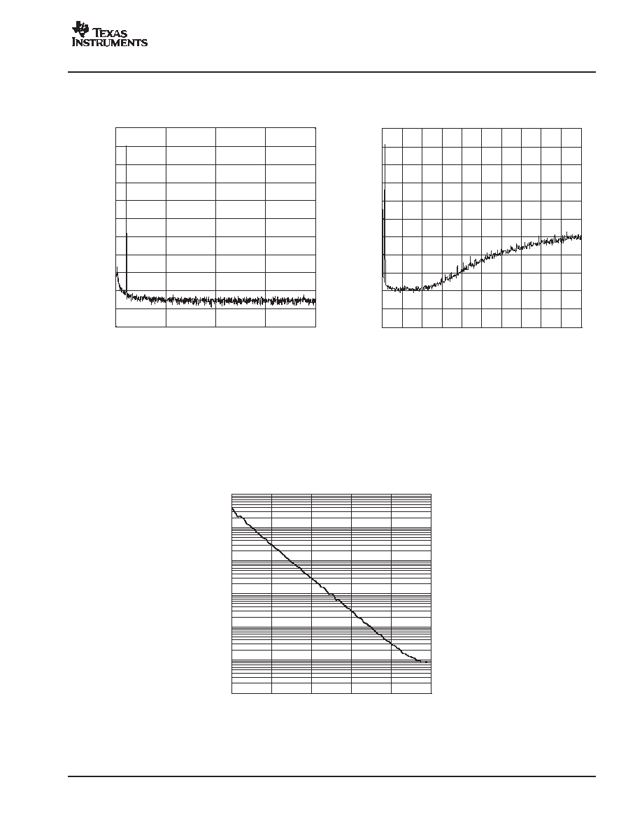
TYPICAL PERFORMANCE CURVES
DIGITAL FILTER
Digital Filter Response
Figure 1. Frequency Response, Sharp Rolloff
Frequency [
×
fS]
-160
-140
-120
-100
-80
-60
-40
-20
0
0
1
2
3
4
Amplitude - dB
AMPLITUDE
vs
FREQUENCY
Figure 2. Pass-Band Ripple, Sharp Rolloff
Frequency [
×
fS]
-3
-2
-1
0
1
2
3
0.0
0.1
0.2
0.3
0.4
0.5
AMPLITUDE
vs
FREQUENCY
0.003
0
-0.001
-0.003
0.001
0.002
-0.002
Amplitude - dB
Figure 3. Frequency Response, Slow Rolloff
Frequency [
×
fS]
-140
-120
-100
-80
-60
-40
-20
0
0
1
2
3
4
Amplitude - dB
AMPLITUDE
vs
FREQUENCY
Figure 4. Transition Characteristics, Slow Rolloff
Frequency [
×
fS]
-20
-18
-16
-14
-12
-10
-8
-6
-4
-2
0
0.0
0.1
0.2
0.3
0.4
0.5
0.6
Amplitude - dB
AMPLITUDE
vs
FREQUENCY
PCM1791A
SLES071A - MARCH 2003 - REVISED JANUARY 2004
www.ti.com
9
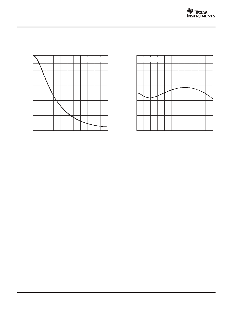
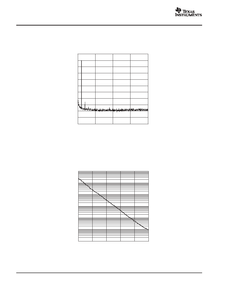
De-Emphasis Filter
Figure 5
f - Frequency - kHz
-10
-9
-8
-7
-6
-5
-4
-3
-2
-1
0
0
2
4
6
8
10
12
14
De-emphasis Level - dB
DE-EMPHASIS LEVEL
vs
FREQUENCY
fS = 32 kHz
Figure 6
f - Frequency - kHz
-0.5
-0.4
-0.3
-0.2
-0.1
-0.0
0.1
0.2
0.3
0.4
0.5
0
2
4
6
8
10
12
14
DE-EMPHASIS ERROR
vs
FREQUENCY
fS = 32 kHz
De-emphasis Error - dB
0.0
Figure 7
f - Frequency - kHz
-10
-9
-8
-7
-6
-5
-4
-3
-2
-1
0
0
2
4
6
8
10
12
14
16
18
20
De-emphasis Level - dB
DE-EMPHASIS LEVEL
vs
FREQUENCY
fS = 44.1 kHz
Figure 8
f - Frequency - kHz
-0.5
-0.4
-0.3
-0.2
-0.1
-0.0
0.1
0.2
0.3
0.4
0.5
0
2
4
6
8
10
12
14
16
18
20
DE-EMPHASIS ERROR
vs
FREQUENCY
0.0
fS = 44.1 kHz
De-emphasis Error - dB
PCM1791A
SLES071A - MARCH 2003 - REVISED JANUARY 2004
www.ti.com
10
De-Emphasis Filter (Continued)
Figure 9
f - Frequency - kHz
-10
-9
-8
-7
-6
-5
-4
-3
-2
-1
0
0
2
4
6
8
10
12
14
16
18
20
22
De-emphasis Level - dB
DE-EMPHASIS LEVEL
vs
FREQUENCY
fS = 48 kHz
Figure 10
f - Frequency - kHz
-0.5
-0.4
-0.3
-0.2
-0.1
-0.0
0.1
0.2
0.3
0.4
0.5
0
2
4
6
8
10
12
14
16
18
20
22
DE-EMPHASIS ERROR
vs
FREQUENCY
fS = 48 kHz
De-emphasis Error - dB
0.0
PCM1791A
SLES071A - MARCH 2003 - REVISED JANUARY 2004
www.ti.com
11
ANALOG DYNAMIC PERFORMANCE
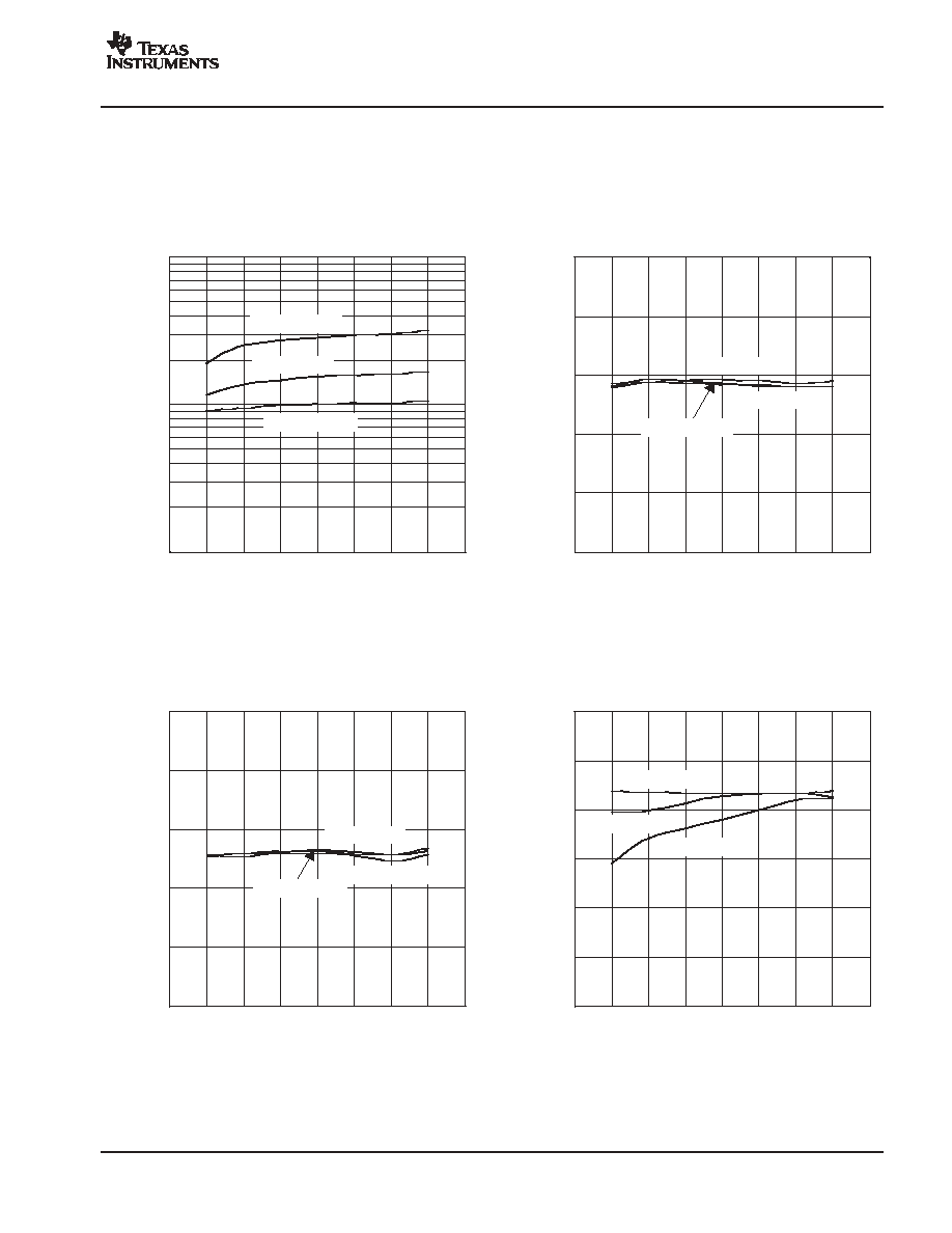
Supply Voltage Characteristics
Figure 11
4.00
4.25
4.50
4.75
5.00
5.25
5.50
5.75
6.00
VCC - Supply Voltage - V
TOTAL HARMONIC DISTORTION + NOISE
vs
SUPPLY VOLTAGE
0.01
0.001
0.0001
fS = 192 kHz
fS = 96 kHz
THD+N - T
otal Harmonic Distortion + Noise - %
fS = 44.1 kHz
Figure 12
VCC - Supply Voltage - V
108
110
112
114
116
118
4.00
4.25
4.50
4.75
5.00
5.25
5.50
5.75
6.00
Dynamic Range - dB
DYNAMIC RANGE
vs
SUPPLY VOLTAGE
fS = 96 kHz
fS = 44.1 kHz
fS = 192 kHz
Figure 13
VCC - Supply Voltage - V
108
110
112
114
116
118
4.00
4.25
4.50
4.75
5.00
5.25
5.50
5.75
6.00
SNR - Signal-to-Noise Ratio - dB
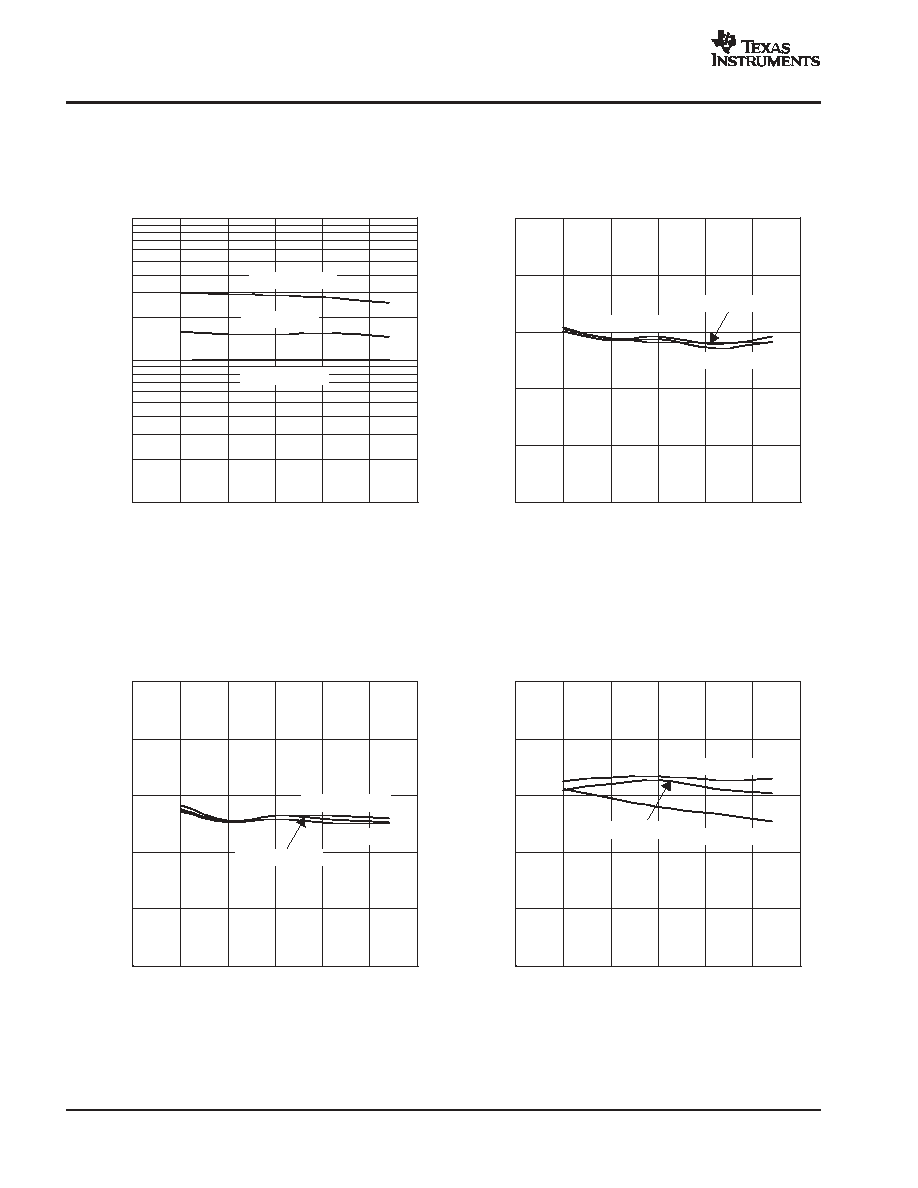
SIGNAL-to-NOISE RATIO
vs
SUPPLY VOLTAGE
fS = 96 kHz
fS = 192 kHz
fS = 44.1 kHz
Figure 14
VCC - Supply Voltage - V
102
104
106
108
110
112
114
4.00
4.25
4.50
4.75
5.00
5.25
5.50
5.75
6.00
Channel Separation - dB
CHANNEL SEPARATION
vs
SUPPLY VOLTAGE
fS = 96 kHz
fS = 192 kHz
fS = 44.1 kHz
NOTE: PCM mode, TA = 25
°
C, VDD = 3.3 V.
PCM1791A
SLES071A - MARCH 2003 - REVISED JANUARY 2004
www.ti.com
12
Temperature Characteristics
Figure 15
-50
-25
0
25
50
75
100
TOTAL HARMONIC DISTORTION + NOISE
vs
FREE-AIR TEMPERATURE
0.01
0.001
0.0001
fS = 192 kHz
fS = 96 kHz
THD+N - T
otal Harmonic Distortion + Noise - %
fS = 44.1 kHz
TA - Free-Air Temperature -
°
C
Figure 16
TA - Free-Air Temperature -
°
C
108
110
112
114
116
118
-50
-25
0
25
50
75
100
Dynamic Range - dB
DYNAMIC RANGE
vs
FREE-AIR TEMPERATURE
fS = 192 kHz
fS = 44.1 kHz
fS = 96 kHz
Figure 17
TA - Free-Air Temperature -
°
C
108
110
112
114
116
118
-50
-25
0
25
50
75
100
SNR - Signal-to-Noise Ratio - dB
SIGNAL-to-NOISE RATIO
vs
FREE-AIR TEMPERATURE
fS = 96 kHz
fS = 44.1 kHz
fS = 192 kHz
Figure 18
TA - Free-Air Temperature -
°
C
104
106
108
110
112
114
-50
-25
0
25
50
75
100
Channel Separation - dB
CHANNEL SEPARATION
vs
FREE-AIR TEMPERATURE
fS = 192 kHz
fS = 44.1 kHz
fS = 96 kHz
NOTE: PCM mode, VDD = 3.3 V, VCC = 5 V.
PCM1791A
SLES071A - MARCH 2003 - REVISED JANUARY 2004
www.ti.com
13
Figure 19. -60-dB Output Spectrum, BW = 20 kHz
f - Frequency - kHz
-160
-150
-140
-130
-120
-110
-100
-90
-80
-70
-60
-50
0
5
10
15
20
Amplitude - dB
AMPLITUDE vs FREQUENCY
Figure 20. -60-dB Output Spectrum, BW = 100 kHz
f - Frequency - kHz
-160
-150
-140
-130
-120
-110
-100
-90
-80
-70
-60
-50
0
10
20
30
40
50
60
70
80
90
100
Amplitude - dB
AMPLITUDE vs FREQUENCY
NOTE: PCM mode, fS = 44.1 kHz, 32768 points, 8 average, TA = 25
°
C, VDD = 3.3 V, VCC = 5 V.
-100
-80
-60
-40
-20
0
Input Level - dBFS
TOTAL HARMONIC DISTORTION + NOISE
vs
INPUT LEVEL
100
0.1
0.01
0.001
0.0001
THD+N - T
otal Harmonic Distortion + Noise - %
1
10
Figure 21. THD+N vs Input Level, PCM Mode
NOTE: PCM mode, fS = 44.1 kHz, TA = 25
°
C, VDD = 3.3 V, VCC = 5 V.
PCM1791A
SLES071A - MARCH 2003 - REVISED JANUARY 2004
www.ti.com
14
f - Frequency - kHz
-160
-150
-140
-130
-120
-110
-100
-90
-80
-70
-60
-50
0
5
10
15
20
Amplitude - dB
AMPLITUDE
vs
FREQUENCY
Figure 22. -60-dB Output Spectrum, DSD Mode
Figure 23. THD+N vs Input Level, DSD Mode
-90 -80 -70
-60 -50
-40 -30
-20 -10
0
Input Level - dBFS
TOTAL HARMONIC DISTORTION + NOISE
vs
INPUT LEVEL
100
0.1
0.01
0.001
0.0001
THD+N - T
otal Harmonic Distortion + Noise - %
1
10
NOTE: DSD mode (FIR-2), TA = 25
°
C, VDD = 3.3 V, VCC = 5 V.
PCM1791A
SLES071A - MARCH 2003 - REVISED JANUARY 2004
www.ti.com
15
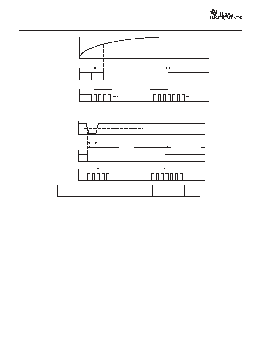
SYSTEM CLOCK AND RESET FUNCTIONS
System Clock Input
The PCM1791A requires a system clock for operating the digital interpolation filters and advanced segment DAC
modulators. The system clock is applied at the SCK input (pin 5). The PCM1791A has a system clock detection circuit
that automatically senses which frequency the system clock is operating. Table 1 shows examples of system clock
frequencies for common audio sampling rates. If the oversampling rate of the delta-sigma modulator is selected as
128 f
S
, the system clock frequency is over 256 f
S
.
Figure 24 shows the timing requirements for the system clock input. For optimal performance, it is important to use
a clock source with low phase jitter and noise. One of the Texas Instruments' PLL1700 family of multiclock generators
is an excellent choice for providing the PCM1791A system clock.
Table 1. System Clock Rates for Common Audio Sampling Frequencies
SAMPLING FREQUENCY
SYSTEM CLOCK FREQUENCY (fSCK) (MHz)
SAMPLING FREQUENCY
128 fS
192 fS
256 fS
384 fS
512 fS
768 fS
32 kHz
4.096(1)
6.144(1)
8.192
12.288
16.384
24.576
44.1 kHz
5.6488(1)
8.4672
11.2896
16.9344
22.5792
33.8688
48 kHz
6.144(1)
9.216
12.288
18.432
24.576
36.864
96 kHz
12.288
18.432
24.576
36.864
49.152(1)
73.728(1)
192 kHz
24.576
36.864
49.152(1)
73.728(1)
(2)
(2)
(1) This system clock rate is not supported in I2C fast mode.
(2) This system clock rate is not supported for the given sampling frequency.
t(SCKH)
System Clock (SCK)
t(SCKL)
2.0 V
0.8 V
H
L
t(SCY)
PARAMETERS
MIN
MAX
UNITS
t(SCY)
System clock pulse cycle time
13
ns
t(SCKH) System clock pulse duration, HIGH
5
ns
t(SCKL) System clock pulse duration, LOW
5
ns
Figure 24. System Clock Input Timing
Power-On and External Reset Functions
The PCM1791A includes a power-on reset function. Figure 25 shows the operation of this function. With V
DD
> 2 V,
the power-on reset function is enabled. The initialization sequence requires 1024 system clocks from the time
V
DD
> 2 V. After the initialization period, the PCM1791A is set to its default reset state, as described in the MODE
CONTROL REGISTERS section of this data sheet.
The PCM1791A also includes an external reset capability using the RST input (pin 6). This allows an external
controller or master reset circuit to force the PCM1791A to initialize to its default reset state.
Figure 26 shows the external reset operation and timing. The RST pin is set to logic 0 for a minimum of 20 ns. The
RST pin is then set to a logic 1 state, thus starting the initialization sequence, which requires 1024 system clock
periods. The external reset is especially useful in applications where there is a delay between the PCM1791A power
up and system clock activation.
PCM1791A
SLES071A - MARCH 2003 - REVISED JANUARY 2004
www.ti.com
16
Reset
Reset Removal
1024 System Clocks
VDD
2.4 V (Max)
2.0 V (Typ)
1.6 V (Min)
Internal Reset
System Clock
Figure 25. Power-On Reset Timing
Reset
Reset Removal
1024 System Clocks
Internal Reset
System Clock
RST (Pin 6)
t(RST)
1.4 V
PARAMETERS
MIN
MAX
UNITS
t(RST)
Reset pulse duration, LOW
20
ns
Figure 26. External Reset Timing
PCM1791A
SLES071A - MARCH 2003 - REVISED JANUARY 2004
www.ti.com
17
AUDIO DATA INTERFACE
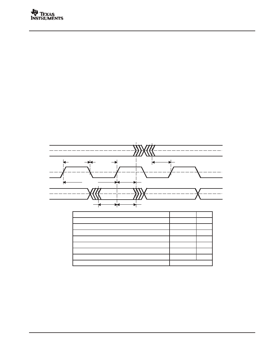
Audio Serial Interface
The audio interface port is a 3-wire serial port. It includes LRCK (pin 1), BCK (pin 2), and DATA (pin 3). BCK is the
serial audio bit clock, and it is used to clock the serial data present on DATA into the serial shift register of the audio
interface. Serial data is clocked into the PCM1791A on the rising edge of BCK. LRCK is the serial audio left/right word
clock.
The PCM1791A requires the synchronization of LRCK and the system clock, but does not need a specific phase
relationship between LRCK and the system clock.
If the relationship between LRCK and system clock changes more than
±
6 BCK, internal operation is initialized within
1/f
S
and analog outputs are forced to the bipolar zero level until resynchronization between LRCK and the system
clock is completed.
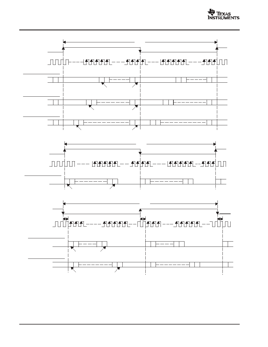
PCM Audio Data Formats and Timing
The PCM1791A supports industry-standard audio data formats, including standard right-justified, I
2
S, and
left-justified. The data formats are shown in Figure 28. Data formats are selected using the format bits, FMT[2:0],
in control register 18. The default data format is 24-bit I
2
S. All formats require binary 2s complement, MSB-first audio
data. Figure 27 shows a detailed timing diagram for the serial audio interface.
DATA
t(BCH)
1.4 V
BCK
LRCK
t(BCL)
t(LB)
t(BCY)
t(DS)
t(DH)
1.4 V
1.4 V
t(BL)
PARAMETERS
MIN
MAX
UNITS
t(BCY)
BCK pulse cycle time
70
ns
t(BCL)
BCK pulse duration, LOW
30
ns
t(BCH)
BCK pulse duration, HIGH
30
ns
t(BL)
BCK rising edge to LRCK edge
10
ns
t(LB)
LRCK edge to BCK rising edge
10
ns
t(DS)
DATA setup time
10
ns
t(DH)
DATA hold time
10
ns
--
LRCK clock data
50%
±
2 bit clocks
Figure 27. Timing of Audio Interface
PCM1791A
SLES071A - MARCH 2003 - REVISED JANUARY 2004
www.ti.com
18
(1) Standard Data Format (Right Justified) ; L-Channel = HIGH, R-Channel = LOW
14 15 16
1
2
15 16
MSB
LSB
1
2
15 16
18 19 20
MSB
LSB
1
2
19 20
1
2
19 20
22 23 24
LSB
1
23
2
24
1
23
2
24
BCK
L-Channel
DATA
R-Channel
1/fS
DATA
DATA
LRCK
Audio Data Word = 16-Bit
Audio Data Word = 20-Bit
Audio Data Word = 24-Bit
MSB
(2) Left Justified Data Format; L-Channel = HIGH, R-Channel = LOW
2
1
MSB
LSB
1
2
24
1
2
24
BCK
L-Channel
DATA
R-Channel
1/fS
LRCK
Audio Data Word = 24-Bit
23
23
(3) I
2
S Data Format; L-Channel = LOW, R-Channel = HIGH
LSB
1
2
24
2
1
1
2
24
2
1
LSB
1
2
16
1
2
16
15
15
23
23
BCK
L-Channel
DATA
R-Channel
1/fS
LRCK
Audio Data Word = 24-Bit
DATA
Audio Data Word = 16-Bit
MSB
MSB
Figure 28. Audio Data Input Formats

PCM1791A
SLES071A - MARCH 2003 - REVISED JANUARY 2004
www.ti.com
19
External Digital Filter Interface and Timing
The PCM1791A supports an external digital filter interface comprising a 4-wire synchronous serial port, which allows
the use of an external digital filter. External filters include the Texas Instruments DF1704 and DF1706, the Pacific
Microsonics PMD200, or a programmable digital signal processor.
In the external DF mode, LRCK (pin 1), BCK (pin 2), DATA (pin 3), and MUTE (pin 4) are defined as WDCK, the word
clock; BCK, the bit clock; DATAL, the L-channel data; and DATAR, the R-channel data, respectively. The external
digital filter interface is selected by using the DFTH bit of control register 20, which functions to bypass the internal
digital filter of the PCM1791A.
Detailed information for the external digital filter interface mode is provided in the APPLICATION FOR EXTERNAL
DIGITAL FILTER INTERFACE section of this data sheet.
Direct Stream Digital (DSD) Format Interface and Timing
The PCM1791A supports the DSD format interface operation, which includes out-of-band noise filtering using an
internal analog FIR filter. For DSD operation, SCK (pin 5) is redefined as BCK, DATA (pin 3) as DATAL (left-channel
audio data), and LRCK (pin 1) as DATAR (right-channel audio data). BCK (pin 2) must be forced low in the DSD mode.
The DSD format (DSD mode) interface is activated by setting the DSD bit of control register 20.
Detailed information for the DSD mode is provided in the APPLICATION FOR DSD FORMAT (DSD MODE)
INTERFACE section of this data sheet.
TDMCA Interface
The PCM1791A supports the time-division-multiplexed command and audio (TDMCA) data format to enable control
of and communication with a number of external devices over a single serial interface.
Detailed information for the TDMCA format is provided in the TDMCA INTERFACE FORMAT section of this data
sheet.
PCM1791A
SLES071A - MARCH 2003 - REVISED JANUARY 2004
www.ti.com
20
FUNCTION DESCRIPTIONS
Zero Detect
The PCM1791A has a zero-detect function. When the PCM1791A detects the zero conditions as shown in Table 2,
the PCM1791A sets ZEROL (pin 23) and ZEROR (pin 22) to HIGH.
Table 2. Zero Conditions
MODE
DETECTING CONDITION AND TIME
PCM
DATA is continuously LOW for 1024 LRCKs.
External DF mode
DATA is continuously LOW for 8
×
1024 WDCKs.
DSD
DZ0
There are an equal number of 1s and 0s in every 8 bits of DSD input data for 23 ms.
DSD
DZ1
The input data is 1001 0110 continuously for 23 ms.
Soft Mute
The PCM1791A supports the mute operation by both hardware and software control. When MUTE (pin 4) is set to
HIGH, or the MUTE bit in mode register 18 is set to 1, both analog outputs are attenuated to the bipolar zero level
in a series of 0.5-dB steps. The duration of the steps is controlled by the setting of the ATS0 and ATS1 bits in mode
register 19.
Serial Control Interface
The PCM1791A supports SPI and I
2
C that sets mode control registers as shown in Table 4. The serial control
interface is selected by MSEL (pin 24); SPI is activated when MSEL is set to LOW, and I
2
C is activated when MSEL
is set to HIGH.
SPI Interface
The SPI interface is a 4-wire synchronous serial port which operates asynchronously to the serial audio interface and
the system clock (SCK). The serial control interface is used to program and read the on-chip mode registers. The
control interface includes MDO (pin 25), MDI (pin 26), MC (pin 27), and MS (pin 28). MDO is the serial data output,
used to read back the values of the mode registers; MDI is the serial data input, used to program the mode registers;
MC is the serial bit clock, used to shift data in and out of the control port, and MS is the mode control enable, used
to enable the internal mode register access.
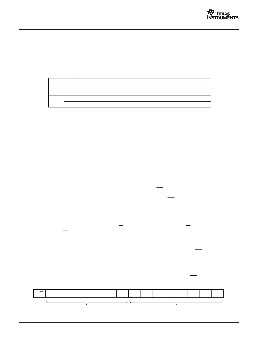
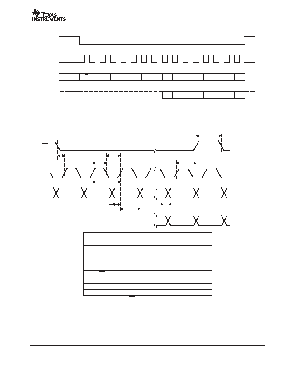
Register Read/Write Operation
All read/write operations for the serial control port use 16-bit data words. Figure 29 shows the control data word
format. The most significant bit is the read/write (R/W) bit. For write operations, the R/W bit must be set to 0. For
read operations, the R/W bit must be set to 1. There are seven bits, labeled IDX[6:0], that hold the register index (or
address) for the read and write operations. The least significant eight bits, D[7:0], contain the data to be written to,
or the data that was read from, the register specified by IDX[6:0].
Figure 30 shows the functional timing diagram for writing or reading the serial control port. MS is held at a logic 1
state until a register needs to be written or read. To start the register write or read cycle, MS is set to logic 0. Sixteen
clocks are then provided on MC, corresponding to the 16 bits of the control data word on MDI and readback data
on MDO. After the eighth clock cycle has completed, the data from the indexed-mode control register appears on
MDO during the read operation. After the sixteenth clock cycle has completed, the data is latched into the
indexed-mode control register during the write operation. To write or read subsequent data, MS must be set to 1 once.
MSB
LSB
Register Index (or Address)
Register Data
R/W
IDX6
IDX5
IDX4
IDX3
IDX2
IDX1
IDX0
D7
D6
D4
D5
D3
D2
D1
D0
Figure 29. Control Data Word Format for MDI
PCM1791A
SLES071A - MARCH 2003 - REVISED JANUARY 2004
www.ti.com
21
High Impedance
When Read Mode is Instructed
A0
D7
D6
D4
D5
D3
D2
D1
D0
D7
D6
D4
D5
D3
D2
D1
D0
R/W
A1
A2
A3
A4
A5
A6
MS
MC
MDI
MDO
NOTE: Bit 15 is used for selection of write or read. Setting R/W = 0 indicates a write, while R/W = 1 indicates a read. Bits 14-8 are used for the register
address. Bits 70 are used for register data.
Figure 30. Serial Control Format
t(MCH)
1.4 V
MS
t(MSS)
LSB
1.4 V
1.4 V
t(MCL)
t(MHH)
t(MSH)
t(MCY)
t(MDH)
t(MDS)
MC
MDI
50% of VDD
MDO
t(MOS)
PARAMETER
MIN
MAX
UNITS
t(MCY) MC pulse cycle time
100
ns
t(MCL) MC low-level time
40
ns
t(MCH) MC high-level time
40
ns
t(MHH) MS high-level time
80
ns
t(MSS) MS falling edge to MC rising edge
15
ns
t(MSH) MS hold time(1)
15
ns
t(MDH) MDI hold time
15
ns
t(MDS) MDI setup time
15
ns
t(MOS) MC falling edge to MDO stable
30
ns
(1) MC rising edge for LSB to MS rising edge
Figure 31. Control Interface Timing
PCM1791A
SLES071A - MARCH 2003 - REVISED JANUARY 2004
www.ti.com
22
I
2
C Interface
The PCM1791A supports the I
2
C serial bus and the data transmission protocol for standard and fast mode as a slave
device. This protocol is explained in I
2
C specification 2.0.
In I
2
C mode, the control terminals are changed as follows.
TERMINAL NAME
TDMCA NAME
PROPERTY
DESCRIPTION
MS
ADR0
Input
I2C address 0
MUTE
ADR1
Input
I2C address 1
MC
SCL
Input
I2C clock
MDI
SDA
Input/output
I2C data
Slave Address
MSB
LSB
1
0
0
1
1
ADR1
ADR0
R/W
The PCM1791A has 7 bits for its own slave address. The first five bits (MSBs) of the slave address are factory preset
to 10011. The next two bits of the address byte are the device select bits, which can be user-defined by the ADR1
and ADR0 terminals. A maximum of four PCM1791As can be connected on the same bus at one time. Each
PCM1791A responds when it receives its own slave address.
Packet Protocol
A master device must control packet protocol, which consists of start condition, slave address, read/write bit, data
if write or acknowledge if read, and stop condition. The PCM1791A supports only slave receivers and slave
transmitters.
9
SDA
SCL
St
Start
1-7
8
1-8
9
1-8
9
9
Sp
Stop
Slave Address
ACK
DATA
ACK
DATA
ACK
ACK
Condition
Condition
R/W
R/W :
Read Operation if 1, Otherwise Write Operation
DATA: 8 Bits (Byte)
ACK:
Acknowledgement of a Byte if 0
NACK: Not Acknowledgement if 1
Write operation
Transmitter
M
M
M
S
M
S
M
S
...
S
M
Data Type
St
Slave address
W
ACK
DATA
ACK
DATA
ACK
...
ACK
Sp
Read operation
Transmitter
M
M
M
S
S
M
S
M
...
M
M
Data Type
St
Slave address
R
ACK
DATA
ACK
DATA
ACK
...
NACK
Sp
NOTE: M: Master device
S: Slave device
St: Start condition
Sp: Stop condition
W: Write
R: Read
Figure 32. Basic I
2
C Framework
PCM1791A
SLES071A - MARCH 2003 - REVISED JANUARY 2004
www.ti.com
23
Write Register
A master can write to any PCM1791A registers using single or multiple accesses. The master sends a PCM1791A
slave address with a write bit, a register address, and the data. If multiple access is required, the address is that of
the starting register, followed by the data to be transferred. When the data are received properly, the index register
is incremented automatically by 1. When the index register reaches 0x7F, the next value is 0x0. When undefined
registers are accessed, the PCM1791A does not send an acknowledgement. Figure 33 is a diagram of the write
operation.
Transmitter
M
M
M
S
M
S
M
S
M
S
...
S
M
Data Type
St
Slave address
W
ACK
Register
address
ACK
Write data 1
ACK
Write data 2
ACK
...
ACK
Sp
M: Master device
S: Slave device
St: Start condition
ACK: Acknowledge
Sp: Stop condition
W: Write
Figure 33. Write Operation
Read Register
A master can read the PCM1791A register. The value of the register address is stored in an indirect index register
in advance. The master sends a PCM1791A slave address with a read bit after storing the register address. Then
the PCM1791A transfers the data which the index register points to. When the data are transferred during a multiple
access, the index register is incremented by 1 automatically. (When first going into read mode immediately following
a write, the index register is not incremented. The master can read the register that was previously written.) When
the index register reaches 0x7F, the next value is 0x0. The PCM1791A outputs some data when the index register
is 0x10 to 0x1F, even if it is not defined in Table 4. Figure 34 is a diagram of the read operation.
Transmitter
M
M
M
S
M
S
M
M
M
S
S
M
...
M
M
Data Type
St
Slave
address
W
ACK
Register
address
ACK
Sr
Slave
address
R
ACK
Data
ACK
...
NACK
Sp
M: Master device
S: Slave device
St: Start condition
Sr: Repeated start condition
ACK: Acknowledge
Sp: Stop condition
NACK: Not Acknowledge
W: Write
R: Read
NOTE: The slave address after the repeat start condition must be the same as the previous slave address.
Figure 34. Read Operation
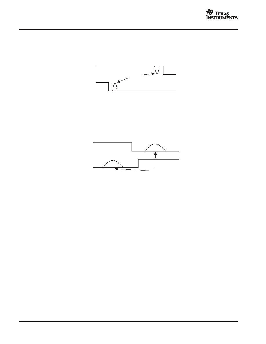
Noise Suppression
The PCM1791A incorporates noise suppression using the system clock (SCK). However, there must be no more than
two noise spikes in 600 ns. The noise suppression works for SCK frequencies between 8 MHz and 40 MHz in fast
mode. However, it works incorrectly in the particular following conditions.
Case 1:
1.
t
(SCK)
> 120 ns (t
(SCK)
: period of SCK)
2.
t
(HI)
+ t
(D-HD)
< t
(SCK)
×
5
3.
Spike noise exists on the first half of the SCL HIGH pulse.
4.
Spike noise exists on the SDA HIGH pulse just before SDA goes LOW.
SCL
SDA
Noise
When these conditions occur at the same time, the data is recognized as LOW.
PCM1791A
SLES071A - MARCH 2003 - REVISED JANUARY 2004
www.ti.com
24
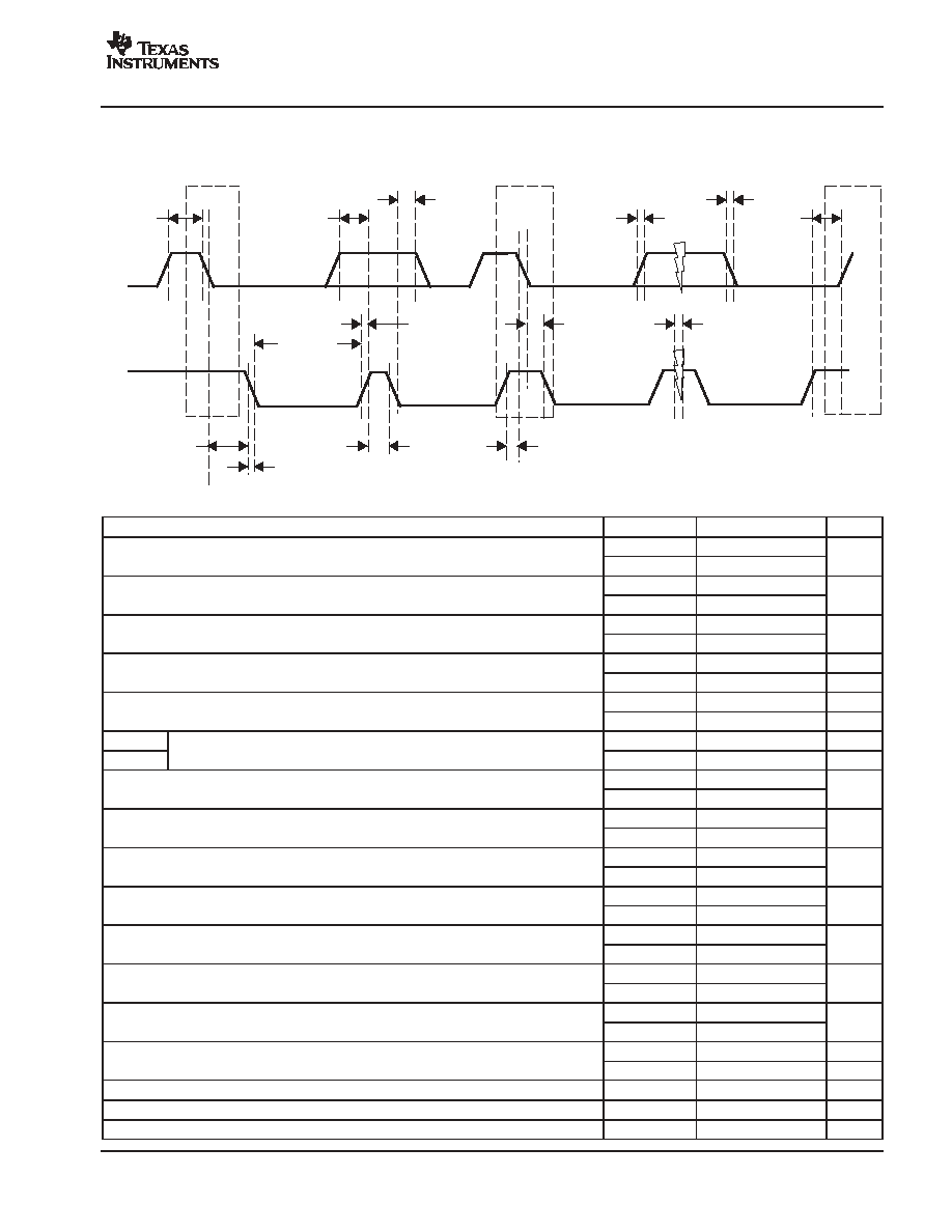
Case 2:
1.
t
(SCK)
> 120 ns
2.
t
(S-HD)
or t
(RS-HD)
< t
(SCK)
×
5
3.
Spike noise exists on both SCL and SDA during the hold time.
SCL
SDA
Noise
When these conditions occur at the same time, the PCM1791A fails to detect a start condition.
Case 3:
1.
t
(SCK)
< 50 ns
2.
t
(SP)
> t
(SCK)
3.
Spike noise exists on SCL just after SCL goes LOW.
4.
Spike noise exists on SDA just before SCL goes LOW.
SCL
SDA
Noise
When these conditions occur at the same time, the PCM1791A erroneously detects a start or stop condition.
PCM1791A
SLES071A - MARCH 2003 - REVISED JANUARY 2004
www.ti.com
25
TIMING DIAGRAM
SDA
SCL
t(BUF)
t(D-SU)
t(D-HD)
Start
t(LOW)
t(S-HD)
t(SCL-F)
t(SCL-R)
t(HI)
Repeated Start
t(RS-SU)
t(RS-HD)
t(SDA-F)
t(SDA-R)
t(P-SU)
Stop
t(SP)
TIMING CHARACTERISTICS
PARAMETER
CONDITIONS
MIN
MAX
UNIT
f(SCL)
SCL clock frequency
Standard
100
kHz
f(SCL)
SCL clock frequency
Fast
400
kHz
t(BUF)
Bus free time between stop and start conditions
Standard
4.7
µ
s
t(BUF)
Bus free time between stop and start conditions
Fast
1.3
µ
s
t(LOW)
Low period of the SCL clock
Standard
4.7
µ
s
t(LOW)
Low period of the SCL clock
Fast
1.3
µ
s
t(HI)
High period of the SCL clock
Standard
4
µ
s
t(HI)
High period of the SCL clock
Fast
600
ns
t(RS-SU)
Setup time for (repeated) start condition
Standard
4.7
µ
s
t(RS-SU)
Setup time for (repeated) start condition
Fast
600
ns
t(S-HD)
Hold time for (repeated) start condition
Standard
4
µ
s
t(RS-HD)
Hold time for (repeated) start condition
Fast
600
ns
t(D-SU)
Data setup time
Standard
250
ns
t(D-SU)
Data setup time
Fast
100
ns
t(D-HD)
Data hold time
Standard
0
900
ns
t(D-HD)
Data hold time
Fast
0
900
ns
t(SCL-R)
Rise time of SCL signal
Standard
20 + 0.1 CB
1000
ns
t(SCL-R)
Rise time of SCL signal
Fast
20 + 0.1 CB
300
ns
t(SCL-R1)
Rise time of SCL signal after a repeated start condition and after an
Standard
20 + 0.1 CB
1000
ns
t(SCL-R1)
Rise time of SCL signal after a repeated start condition and after an
acknowledge bit
Fast
20 + 0.1 CB
300
ns
t(SCL-F)
Fall time of SCL signal
Standard
20 + 0.1 CB
1000
ns
t(SCL-F)
Fall time of SCL signal
Fast
20 + 0.1 CB
300
ns
t(SDA-R)
Rise time of SDA signal
Standard
20 + 0.1 CB
1000
ns
t(SDA-R)
Rise time of SDA signal
Fast
20 + 0.1 CB
300
ns
t(SDA-F)
Fall time of SDA signal
Standard
20 + 0.1 CB
1000
ns
t(SDA-F)
Fall time of SDA signal
Fast
20 + 0.1 CB
300
ns
t(P-SU)
Setup time for stop condition
Standard
4
µ
s
t(P-SU)
Setup time for stop condition
Fast
600
ns
C(B)
Capacitive load for SDA and SCL lines
400
pF
t(SP)
Pulse duration of suppressed spike
Fast
50
ns
VNH
Noise margin at high level for each connected device (including hysteresis)
0.2 VDD
V
PCM1791A
SLES071A - MARCH 2003 - REVISED JANUARY 2004
www.ti.com
26
MODE CONTROL REGISTERS
User-Programmable Mode Controls
The PCM1791A includes a number of user-programmable functions which are accessed via mode control registers.
The registers are programmed using the serial control interface, which was previously discussed in this data sheet.
Table 3 lists the available mode-control functions, along with their default reset conditions and associated register
index.
Table 3. User-Programmable Function Controls
FUNCTION
DEFAULT
REGISTER
BIT
PCM
DSD
DF
BYPASS
Digital attenuation control
0 dB to 120 dB and mute, 0.5 dB/step
0 dB
Register 16
Register 17
ATL[7:0] (for L-ch)
ATR[7:0] (for R-ch)
yes
Attenuation load control
Disabled, enabled
Attenuation disabled
Register 18
ATLD
yes
Input audio data format selection
16-, 20-, 24-bit standard (right-justified) format
24-bit MSB-first left-justified format
16-/24-bit I2S format
24-bit I2S format
Register 18
FMT[2:0]
yes
yes
Sampling rate selection for de-emphasis
Disabled, 44.1 kHz, 48 kHz, 32 kHz
De-emphasis disabled
Register 18
DMF[1:0]
yes
yes(1)
De-emphasis control
Disabled, enabled
De-emphasis disabled
Register 18
DME
yes
Soft mute control
Mute disabled, enabled
Mute disabled
Register 18
MUTE
yes
Output phase reversal
Normal, reverse
Normal
Register 19
REV
yes
yes
yes
Attenuation speed selection
×
1 fS,
×
(1/2)fS,
×
(1/4)fS,
×
(1/8)fS
×
1 fS
Register 19
ATS[1:0]
yes
DAC operation control
Enabled, disabled
DAC operation enabled
Register 19
OPE
yes
yes
yes
Digital filter rolloff selection
Sharp rolloff, slow rolloff
Sharp rolloff
Register 19
FLT
yes
Infinite zero mute control
Disabled, enabled
Disabled
Register 19
INZD
yes
yes
System reset control
Reset operation , normal operation
Normal operation
Register 20
SRST
yes
yes
yes
DSD interface mode control
DSD enabled, disabled
Disabled
Register 20
DSD
yes
yes
Digital-filter bypass control
DF enabled, DF bypass
DF enabled
Register 20
DFTH
yes
yes
Monaural mode selection
Stereo, monaural
Stereo
Register 20
MONO
yes
yes
yes
Channel selection for monaural mode data
L-channel, R-channel
L-channel
Register 20
CHSL
yes
yes
yes
Delta-sigma oversampling rate selection
×
64 fS,
×
128 fS,
×
32 fS
×
64 fS
Register 20
OS[1:0]
yes
yes(2)
yes
PCM zero output enable
Enabled
Register 21
PCMZ
yes
yes
DSD zero output enable
Disabled
Register 21
DZ[1:0]
yes
Function Available Only for Read
Zero detection flag
Not zero, zero detected
Not zero = 0
Zero detected = 1
Register 22
ZFGL (for L-ch)
ZFGR (for R-ch)
yes
yes
yes
Device ID (at TDMCA)
-
Register 23
ID[4:0]
yes
(1) When in DSD mode, DMF[1:0] is defined as DSD filter (analog FIR) performance selection.
(2) When in DSD mode, OS[1:0] is defined as DSD filter (analog FIR) operation rate selection.
PCM1791A
SLES071A - MARCH 2003 - REVISED JANUARY 2004
www.ti.com
27
Register Map
The mode control register map is shown in Table 4. Registers 1621 include an R/W bit, which determines whether
a register read (R/W = 1) or write (R/W = 0) operation is performed. Registers 22 and 23 are read-only.
Table 4. Mode Control Register Map
B15
B14
B13
B12
B11
B10
B9
B8
B7
B6
B5
B4
B3
B2
B1
B0
Register 16
R/W
0
0
1
0
0
0
0
ATL7
ATL6
ATL5
ATL4
ATL3
ATL2
ATL1
ATL0
Register 17
R/W
0
0
1
0
0
0
1
ATR7
ATR6
ATR5
ATR4
ATR3
ATR2
ATR1
ATR0
Register 18
R/W
0
0
1
0
0
1
0
ATLD
FMT2
FMT1
FMT0
DMF1
DMF0
DME
MUTE
Register 19
R/W
0
0
1
0
0
1
1
REV
ATS1
ATS0
OPE
RSV
RSV
FLT
INZD
Register 20
R/W
0
0
1
0
1
0
0
RSV
SRST
DSD
DFTH
MONO
CHSL
OS1
OS0
Register 21
R/W
0
0
1
0
1
0
1
RSV
RSV
RSV
RSV
RSV
DZ1
DZ0
PCMZ
Register 22
R
0
0
1
0
1
1
0
RSV
RSV
RSV
RSV
RSV
RSV
ZFGR
ZFGL
Register 23
R
0
0
1
0
1
1
1
RSV
RSV
RSV
ID4
ID3
ID2
ID1
ID0
Register Definitions
B15
B14
B13
B12
B11
B10
B9
B8
B7
B6
B5
B4
B3
B2
B1
B0
Register 16
R/W
0
0
1
0
0
0
0
ATL7
ATL6
ATL5
ATL4
ATL3
ATL2
ATL1
ATL0
Register 17
R/W
0
0
1
0
0
0
1
ATR7
ATR6
ATR5
ATR4
ATR3
ATR2
ATR1
ATR0
R/W: Read/Write Mode Select
When R/W = 0, a write operaton is performed.
When R/W = 1, a read operaton is performed.
Default value: 0
ATx[7:0]: Digital Attenuation Level Setting
These bits are available for read and write.
Default value: 1111 1111b
Each DAC output has a digital attenuator associated with it. The attenuator can be set from 0 dB to 120 dB, in 0.5-dB
steps. Alternatively, the attenuator can be set to infinite attenuation (or mute).
The attenuation data for each channel can be set individually. However, the data load control (the ATLD bit of control
register 18) is common to both attenuators. ATLD must be set to 1 in order to change an attenuator setting. The
attenuation level can be set using the following formula:
Attenuation level (dB) = 0.5 dB
·
(ATx[7:0]
DEC
255)
where ATx[7:0]
DEC
= 0 through 255
For ATx[7:0]
DEC
= 0 through 14, the attenuator is set to infinite attenuation. The following table shows attenuation
levels for various settings:
ATx[7:0]
Decimal Value
Attenuation Level Setting
1111 1111b
255
0 dB, no attenuation (default)
1111 1110b
254
0.5 dB
1111 1101b
253
1.0 dB
L
L
L
0001 0000b
16
119.5 dB
0000 1111b
15
120.0 dB
0000 1110b
14
Mute
L
L
L
0000 0000b
0
Mute
PCM1791A
SLES071A - MARCH 2003 - REVISED JANUARY 2004
www.ti.com
28
B15
B14
B13
B12
B11
B10
B9
B8
B7
B6
B5
B4
B3
B2
B1
B0
Register 18
R/W
0
0
1
0
0
1
0
ATLD
FMT2
FMT1
FMT0
DMF1
DMF0
DME
MUTE
R/W: Read/Write Mode Select
When R/W = 0, a write operaton is performed.
When R/W = 1, a read operaton is performed.
Default value: 0
ATLD: Attenuation Load Control
This bit is available for read and write.
Default value: 0
ATLD = 0
Attenuation control disabled (default)
ATLD = 1
Attenuation control enabled
The ATLD bit enables loading of the attenuation data contained in registers 16 and 17. When ATLD = 0, the
attenuation settings remain at the previously programmed levels, ignoring new data loaded from registers 16 and
17. When ATLD = 1, attenuation data written to registers 16 and 17 is loaded normally.
FMT[2:0]: Audio Interface Data Format
These bits are available for read and write.
Default value: 101
FMT[2:0]
Audio Data Format Selection
000
16-bit standard format, right-justified data
001
20-bit standard format, right-justified data
010
24-bit standard format, right-justified data
011
24-bit MSB-first, left-justified format data
100
16-bit I
2
S format data
101
24-bit I
2
S format data (default)
110
Reserved
111
Reserved
The FMT[2:0] bits select the data format for the serial audio interface.
For the external digital filter interface mode (DFTH mode), this register is operated as shown in the
APPLICATION
FOR EXTERNAL DIGITAL FILTER INTERFACE
section of this data sheet.
DMF[1:0]: Sampling Frequency Selection for the De-Emphasis Function
These bits are available for read and write.
Default value: 00
DMF[1:0]
De-Emphasis Sampling Frequency Selection
00
Disabled (default)
01
48 kHz
10
44.1 kHz
11
32 kHz
The DMF[1:0] bits select the sampling frequency used by the digital de-emphasis function when it is enabled by
setting the DME bit. The de-emphasis curves are shown in the TYPICAL PERFORMANCE CURVES section of this
data sheet.
For the DSD mode, analog FIR filter performance can be selected using this register. A register map and filter
response plots are shown in the APPLICATION FOR DSD FORMAT (DSD MODE) INTERFACE section of this data
sheet.
PCM1791A
SLES071A - MARCH 2003 - REVISED JANUARY 2004
www.ti.com
29
DME: Digital De-Emphasis Control
This bit is available for read and write.
Default value: 0
DME = 0
De-emphasis disabled (default)
DME = 1
De-emphasis enabled
The DME bit enables or disables the de-emphasis function for both channels.
MUTE: Soft Mute Control
This bit is available for read and write.
Default value: 0
MUTE = 0
MUTE disabled (default)
MUTE = 1
MUTE enabled
The MUTE bit enables or disables the soft mute function for both channels.
Soft mute is operated as a 256-step attenuator. The speed for each step to
dB (mute) is determined by the
attenuation rate selected in the ATS register.
B15
B14
B13
B12
B11
B10
B9
B8
B7
B6
B5
B4
B3
B2
B1
B0
Register 19
R/W
0
0
1
0
0
1
1
REV
ATS1
ATS0
OPE
RSV
RSV
FLT
INZD
R/W: Read/Write Mode Select
When R/W = 0, a write operaton is performed.
When R/W = 1, a read operaton is performed.
Default value: 0
REV: Output Phase Reversal
This bit is available for read and write.
Default value: 0
REV = 0
Normal output (default)
REV = 1
Inverted output
The REV bit inverts the output phase for both channels.
ATS[1:0]: Attenuation Rate Select
These bits are available for read and write.
Default value: 00
ATS[1:0]
Attenuation Rate Selection
00
Every LRCK (default)
01
LRCK/2
10
LRCK/4
11
LRCK/8
The ATS[1:0] bits select the rate at which the attenuator is decremented/incremented during level transitions.
PCM1791A
SLES071A - MARCH 2003 - REVISED JANUARY 2004
www.ti.com
30
OPE: DAC Operation Control
This bit is available for read and write.
Default value: 0
OPE = 0
DAC operation enabled (default)
OPE = 1
DAC operation disabled
The OPE bit enables or disables the analog output for both channels. Disabling the analog outputs forces them to
the bipolar zero level (BPZ) even if digital audio data is present on the input.
FLT: Digital Filter Rolloff Control
This bit is available for read and write.
Default value: 0
FLT = 0
Sharp rolloff (default)
FLT = 1
Slow rolloff
The FLT bit selects the digital filter rolloff characteristic. The filter responses for these selections are shown in the
TYPICAL PERFORMANCE CURVES section of this data sheet.
INZD: Infinite Zero Detect Mute Control
This bit is available for read and write.
Default value: 0
INZD = 0
Infinite zero detect mute disabled (default)
INZD = 1
Infinite zero detect mute enabled
The INZD bit enables or disables the zero detect mute function. Setting INZD to 1 forces muted analog outputs to
hold a bipolar zero level when the PCM1791A detects a zero condition in both channels. The infinite zero detect mute
function is not available in the DSD mode.
B15
B14
B13
B12
B11
B10
B9
B8
B7
B6
B5
B4
B3
B2
B1
B0
Register 20
R/W
0
0
1
0
1
0
0
RSV
SRST
DSD
DFTH
MONO
CHSL
OS1
OS0
R/W: Read/Write Mode Select
When R/W = 0, a write operaton is performed.
When R/W = 1, a read operaton is performed.
Default value: 0
SRST: System Reset Control
This bit is available for write only.
Default value: 0
SRST = 0
Normal operation (default)
SRST = 1
System reset operation (generate one reset pulse)
The SRST bit resets the PCM1791A to the initial system condition.
DSD: DSD Interface Mode Control
This bit is available for read and write.
Default value: 0
DSD = 0
DSD interface mode disabled (default)
DSD = 1
DSD interface mode enabled
The DSD bit enables or disables the DSD interface mode.
PCM1791A
SLES071A - MARCH 2003 - REVISED JANUARY 2004
www.ti.com
31
DFTH: Digital Filter Bypass (or Through Mode) Control
This bit is available for read and write.
Default value: 0
DFTH = 0
Digital filter enabled (default)
DFTH = 1
Digital filter bypassed for the external digital filter
The DFTH bit enables or disables the external digital filter interface mode.
MONO: Monaural Mode Selection
This bit is available for read and write.
Default value: 0
MONO = 0
Stereo mode (default)
MONO = 1
Monaural mode
The MONO function changes operation mode from the normal stereo mode to the monaural mode. When the
monaural mode is selected, both DACs operate in a balanced mode for one channel of audio input data. Channel
selection is available for L-channel or R-channel data, determined by the setting of the CHSL bit as described
immediately following.
CHSL: Channel Selection for Monaural Mode
This bit is available for read and write.
Default value: 0
CHSL = 0
L-channel selected (default)
CHSL = 1
R-channel selected
This bit is available when MONO = 1.
The CHSL bit selects L-channel or R-channel data to be used in monaural mode. In the DSD mono mode, DATA (pin
3) is used for the input data.
OS[1:0]: Delta-Sigma Oversampling Rate Selection
These bits are available for read and write.
Default value: 00
OS[1:0]
Operation Speed Select
00
64 times f
S
(default)
01
32 times f
S
10
128 times f
S
11
Reserved
The OS bits change the oversampling rate of delta-sigma modulation. Use of this function enables the designer to
stabilize the conditions at the post low-pass filter for different sampling rates. As an application example,
programming to set 128 times in 44.1-kHz operation, 64 times in 96-kHz operation, and 32 times in 192-kHz operation
allows the use of only a single type (cutoff frequency) of post low-pass filter. The 128 f
S
oversampling rate is not
available at sampling rates above 100 kHz. If the 128-f
S
oversampling rate is selected, a system clock of more than
256 f
S
is required.
In DSD mode, these bits select the speed of the bit clock for DSD data coming into the analog FIR filter.
B15
B14
B13
B12
B11
B10
B9
B8
B7
B6
B5
B4
B3
B2
B1
B0
Register 21
R/W
0
0
1
0
1
0
1
RSV
RSV
RSV
RSV
RSV
DZ1
DZ0
PCMZ
R/W: Read/Write Mode Select
When R/W = 0, a write operaton is performed.
When R/W = 1, a read operaton is performed.
Default value: 0
PCM1791A
SLES071A - MARCH 2003 - REVISED JANUARY 2004
www.ti.com
32
DZ[1:0]: DSD Zero Output Enable
These bits are available for read and write.
Default value: 00
DZ[1:0]
Zero Output Enable
00
Disabled (default)
01
Even pattern detect
1x
96
H
pattern detect
The DZ bits enable or disable the output zero flags, and select the zero pattern in the DSD mode.
PCMZ: PCM Zero Output Enable
This bit is available for read and write.
Default value: 1
PCMZ = 0
PCM zero output disabled
PCMZ = 1
PCM zero output enabled (default)
The PCMZ bit enables or disables the output zero flags in the PCM mode and the external DF mode.
B15
B14
B13
B12
B11
B10
B9
B8
B7
B6
B5
B4
B3
B2
B1
B0
Register 22
R
0
0
1
0
1
1
0
RSV
RSV
RSV
RSV
RSV
RSV
ZFGR
ZFGL
R: Read Mode Select
Value is always 1, specifying the readback mode.
ZFGx: Zero-Detection Flag
where x = L or R, corresponding to the DAC output channel. These bits are available only for readback.
Default value: 00
ZFGx = 0
Not zero
ZFGx = 1
Zero detected
These bits show zero conditions. Their status is the same as that of the zero flags at ZEROL (pin 23) and ZEROR
(pin 22). See Zero Detect in the FUNCTION DESCRIPTIONS section.
B15
B14
B13
B12
B11
B10
B9
B8
B7
B6
B5
B4
B3
B2
B1
B0
Register 23
R
0
0
1
0
1
1
1
RSV
RSV
RSV
ID4
ID3
ID2
ID1
ID0
R: Read Mode Select
Value is always 1, specifying the readback mode.
ID[4:0]: Device ID
The ID[4:0] bits hold a device ID in the TDMCA mode.
PCM1791A
SLES071A - MARCH 2003 - REVISED JANUARY 2004
www.ti.com
33
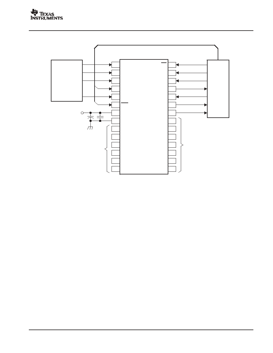
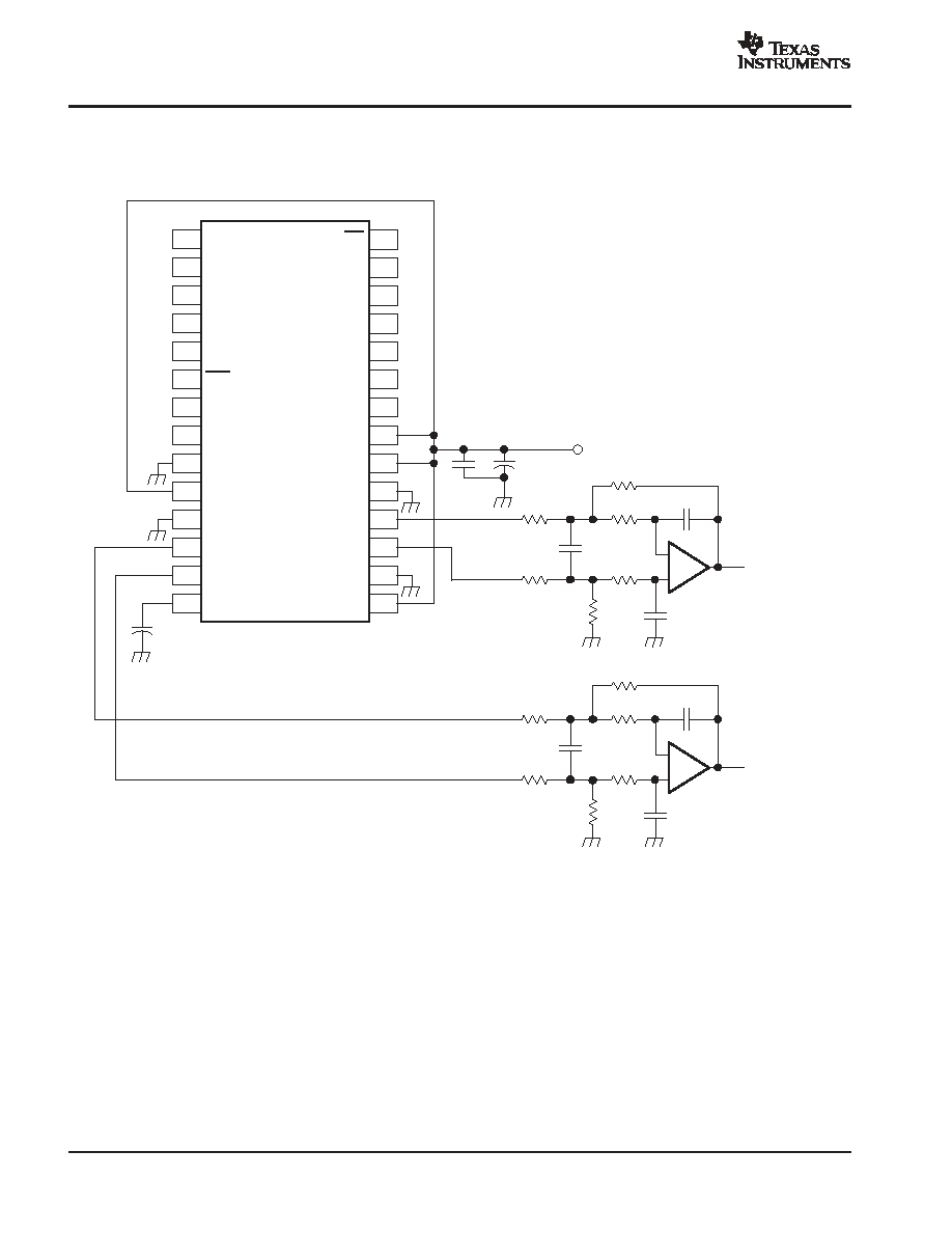
TYPICAL CONNECTION DIAGRAM IN PCM MODE
SCK
24
23
22
21
20
19
18
17
16
15
5
6
7
8
9
10
11
12
13
14
PCM1791A
RST
VDD
DGND
AGNDF
VCCR
AGNDR
VOUTR-
VOUTR+
VCOM
MSEL
VOUTL-
ZEROL
ZEROR
VCCF
VCCL
VOUTL+
AGNDC
AGNDL
LRCK
1
2
3
4
BCK
DATA
MUTE
28
27
26
25
MS
MC
MDI
MDO
VCCC
Controller
L/R Clock (fS)
Bit Clock
Audio Data
System Clock
+
3.3 V
Analog
Output Stage
(See Figure 36)
Analog
Output Stage
(See Figure 36)
Figure 35. Typical Application Circuit for Standard PCM Audio Operation
PCM1791A
SLES071A - MARCH 2003 - REVISED JANUARY 2004
www.ti.com
34
APPLICATION INFORMATION
ANALOG OUTPUTS
SCK
24
23
22
21
20
19
18
17
16
15
5
6
7
8
9
10
11
12
13
14
PCM1791A
RST
VDD
DGND
AGNDF
VCCR
AGNDR
VOUTR-
VOUTR+
VCOM
MSEL
VOUTL-
ZEROL
ZEROR
VCCF
VCCL
VOUTL+
AGNDC
AGNDL
LRCK
1
2
3
4
BCK
DATA
MUTE
28
27
26
25
MS
MC
MDI
MDO
VCCC
+
1
µ
F
-
+
C3L
R6L
R4L
R5L
C1L
C2L
R3L
R2L
R1L
VOUT
L-Channel
+
5 V
-
+
VOUT
R-Channel
10
µ
F
0.1
µ
F
C3R
R6R
R4R
R5R
C1R
C2R
R3R
R2R
R1R
NOTE: Example R and C values for fC = 77 kHz R1, R2: 1.8 k
, R3,R4: 3.3 k
, R5,R6: 680
, C1: 1800 pF, C2, C3: 560 pF.
Figure 36. Typical Application for Analog Output Stage
Analog Output Level and LPF
The signal level of the DAC differential-voltage output {(V
OUT
L+)(V
OUT
L), (V
OUT
R+)(V
OUT
R)} is 3.2 Vp-p
at 0 dB (full scale). The voltage output of the LPF is given by following equation:
V
OUT
= 3.2 Vp-p
×
(R
f
/R
i
)
Here, R
f
is the feedback resistor in the LPF, and R
3
= R
4
in a typical application circuit. R
i
is the input resistor
in the LPF, and R
1
= R
2
in a typical application circuit.
Op Amp for LPF
An OPA2134 or 5532 type op amp is recommended for the LPF circuit to obtain the specified audio
performance. Dynamic performance such as gain bandwidth, settling time, and slew rate of the op amp largely
determines the audio dynamic performance of the LPF section. The input noise specification of the op amp
should be considered to obtain a 113-dB S/N ratio.
PCM1791A
SLES071A - MARCH 2003 - REVISED JANUARY 2004
www.ti.com
35
Analog Gain of Balanced Amplifier
The DAC voltage outputs are followed by balanced amplifier stages, which sum the differential signals for each
channel, creating a single-ended voltage output. In addition, the balanced amplifiers provide a third-order
low-pass filter function, which band limits the audio output signal. The cutoff frequency and gain are determined
by external R and C component values. In this case, the cutoff frequency is 77 kHz with a gain of 1.83. The
output voltage for each channel is 5.9 Vp-p, or 2.1 V rms.
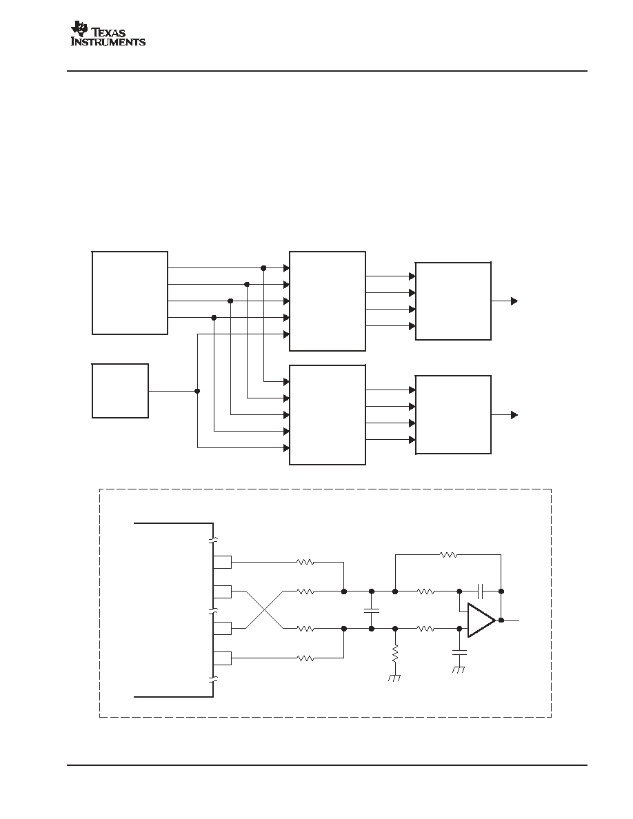
Application for Monaural-Mode Operation
A single-channel signal from the stereo audio data input is output from both V
OUT
L and V
OUT
R as a differential
output. The channel to be output is selected by setting the CHSL bit in register 20. The advantage of monaural
operation is to provide over 115 dB of dynamic range for high-end audio applications.
-
+
C3
C1
C2
R2
18
17
13
12
PCM1791A
VOUTR+
VOUTL-
VOUTL+
VOUTR-
R4
R1
R3
R5
R6
R8
R7
L/R Clock
Bit Clock
System Clock
Audio Data
PCM1791A
PCM1791A
Controller
Analog
Output
Stage
VOUT
R-Channel
Analog
Output
Stage
VOUT
L-Channel
Analog Output Stage
NOTE: Example R and C values for fC = 77 kHz, R1R4: 3.6 k
, R5, R6: 3.3 k
, R7, R8: 680
, C1: 1800 pF, C2, C3: 560 pF.
Figure 37. Connection Diagram for Monaural Mode Interface
PCM1791A
SLES071A - MARCH 2003 - REVISED JANUARY 2004
www.ti.com
36
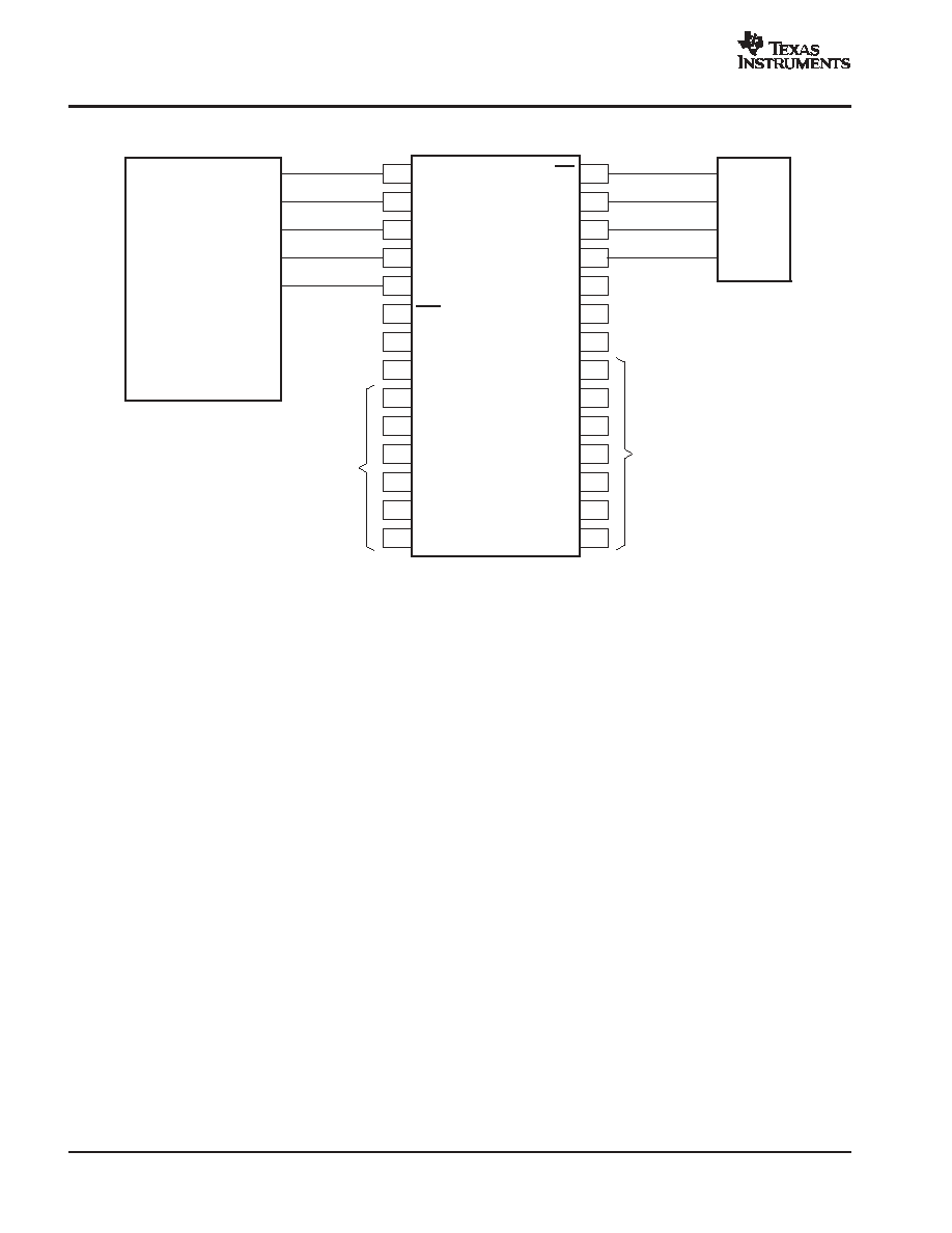
APPLICATION FOR EXTERNAL DIGITAL FILTER INTERFACE
SCK
24
23
22
21
20
19
18
17
16
15
5
6
7
8
9
10
11
12
13
14
PCM1791A
RST
VDD
DGND
AGNDF
VCCR
AGNDR
VOUTR-
VOUTR+
VCOM
MSEL
VOUTL-
ZEROL
ZEROR
VCCF
VCCL
VOUTL+
AGNDC
AGNDL
LRCK
1
2
3
4
BCK
DATA
MUTE
28
27
26
25
MS
MC
MDI
MDO
VCCC
Mode
Control
WDCK (Word Clock)
BCK
DATA-L
SCK
Analog
Output Stage
(Same as Standard
Application)
Analog
Output Stage
(Same as Standard
Application)
DF1704
DF1706
PMD200
DATA-R
Figure 38. Connection Diagram for External DIgital Filter (Internal DF Bypass Mode) Application
Application for Interfacing With an External Digital Filter
For some applications, it may be desirable to use an external digital filter to perform the interpolation function, as it
can provide improved stop-band attenuation when compared to the internal digital filter of the PCM1791A.
The PCM1791A supports several external digital filters, including:
D
Texas Instruments DF1704 and DF1706
D
Pacific Microsonics PMD200 HDCD filter/decoder IC
D
Programmable digital signal processors
The external digital filter application mode is accessed by programming the following bit in the corresponding control
register:
D
DFTH = 1 (register 20)
The pins used to provide the serial interface for the external digital filter are shown in the connection diagram of
Figure 38. The word clock (WDCK) signals must be operated at 8
×
or 4
×
the desired sampling frequency, f
S
.
Pin Assignments When Using the External Digital Filter Interface
D
LRCK (pin 1): WDCK as word clock input
D
BCK (pin 2): BCK as bit clock for audio data
D
DATA (pin 3): DATAL as L-channel audio data input
D
MUTE (pin 4): DATAR as R-channel audio data input
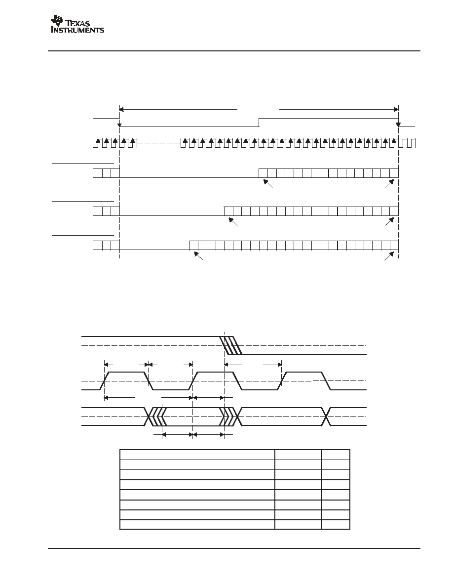
PCM1791A
SLES071A - MARCH 2003 - REVISED JANUARY 2004
www.ti.com
37
Audio Format
The PCM1791A in the external digital filter interface mode supports right-justified audio formats including 16-bit,
20-bit, and 24-bit audio data, as shown in Figure 39. The audio format is selected by the FMT[2:0] bits of control
register 18.
MSB
LSB
16
BCK
DATAL
DATAR
1/4 fS or 1/8 fS
WDCK
Audio Data Word = 16-Bit
Audio Data Word = 20-Bit
Audio Data Word = 24-Bit
1
2
3
4
5
6
7
8
9 10 11 12 13 14 15
16
15
MSB
LSB
16
1
2
3
4
5
6
7
8
9 10 11 12 13 14 15
20
19
20
17 18 19
MSB
LSB
16
1
2
3
4
5
6
7
8
9 10 11 12 13 14 15
24
23
20
17 18 19
24
21 22 23
DATAL
DATAR
DATAL
DATAR
Figure 39. Audio Data Input Format for External Digital Filter (Internal DF Bypass Mode) Application
System Clock (SCK) and Interface Timing
The PCM1791A in an application using an external digital filter requires the synchronization of WDCK and the system
clock. The system clock is phase-free with respect to WDCK. Interface timing among WDCK, BCK, DATAL, and
DATAR is shown in Figure 40.
DATAL
DATAR
t(BCH)
1.4 V
BCK
WDCK
t(BCL)
t(LB)
t(BCY)
t(DS)
t(DH)
1.4 V
1.4 V
t(BL)
PARAMETER
MIN
MAX
UNITS
t(BCY) BCK pulse cycle time
20
ns
t(BCL) BCK pulse duration, LOW
7
ns
t(BCH) BCK pulse duration, HIGH
7
ns
t(BL)
BCK rising edge to WDCK falling edge
5
ns
t(LB)
WDCK falling edge to BCK rising edge
5
ns
t(DS)
DATAL, DATAR setup time
5
ns
t(DH)
DATAL, DATAR hold time
5
ns
Figure 40. Audio Interface Timing for External Digital Filter (Internal DF Bypass Mode) Application
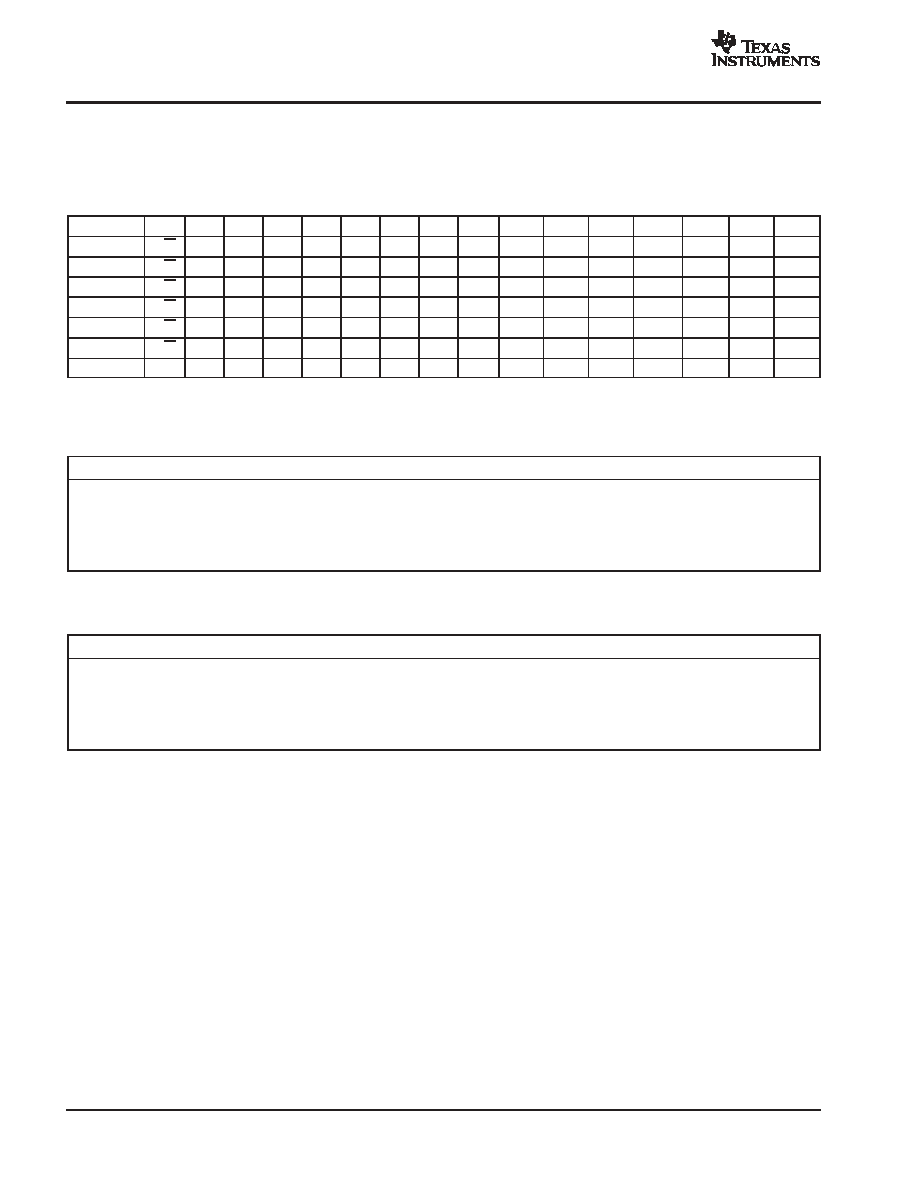
PCM1791A
SLES071A - MARCH 2003 - REVISED JANUARY 2004
www.ti.com
38
Functions Available in the External Digital Filter Mode
The external digital filter mode allows access to the majority of the PCM1791A mode control functions.
The following table shows the register mapping available when the external digital filter mode is selected, along with
descriptions of functions which are modified when using this mode selection.
B15
B14
B13
B12
B11
B10
B9
B8
B7
B6
B5
B4
B3
B2
B1
B0
Register 16
R/W
0
0
1
0
0
0
0
-
-
-
-
-
-
-
-
Register 17
R/W
0
0
1
0
0
0
1
-
-
-
-
-
-
-
-
Register 18
R/W
0
0
1
0
0
1
0
-
FMT2
FMT1
FMT0
-
-
-
-
Register 19
R/W
0
0
1
0
0
1
1
REV
-
-
OPE
-
-
-
INZD
Register 20
R/W
0
0
1
0
1
0
0
-
SRST
0
1
MONO
CHSL
OS1
OS0
Register 21
R/W
0
0
1
0
1
0
1
-
-
-
-
-
-
-
PCMZ
Register 22
R
0
0
1
0
1
1
0
-
-
-
-
-
-
ZFGR
ZFGL
NOTE: -: Function is disabled. No operation even if data bit is set
FMT[2:0]: Audio Data Format Selection
Default value: 000
FMT[2:0]
Audio Data Format Select
000
16-bit right-justified format (default)
001
20-bit right-justified format
010
24-bit right-justified format
Other
N/A
OS[1:0]: Delta-Sigma Modulator Oversampling Rate Selection
Default value: 00
OS[1:0]
Operation Speed Select
00
8 times WDCK (default)
01
4 times WDCK
10
16 times WDCK
11
Reserved
The effective oversampling rate is determined by the oversampling performed by both the external digital filter and
the delta-sigma modulator. For example, if the external digital filter is 8
×
oversampling, and the user selects
OS[1:0] = 00, then the delta-sigma modulator oversamples by 8
×
, resulting in an effective oversampling rate of 64
×
.
The 16
×
WDCK oversampling rate is not available above a 100-kHz sampling rate. If the oversampling rate selected
is 16
×
WDCK, the system clock frequency must be over 256 f
S
.
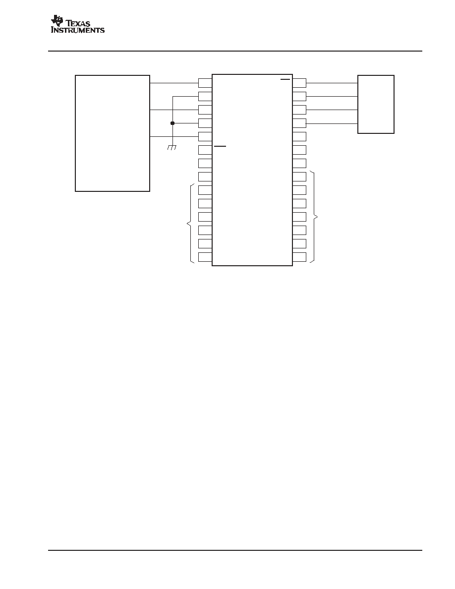
PCM1791A
SLES071A - MARCH 2003 - REVISED JANUARY 2004
www.ti.com
39
APPLICATION FOR DSD FORMAT (DSD MODE) INTERFACE
SCK
24
23
22
21
20
19
18
17
16
15
5
6
7
8
9
10
11
12
13
14
PCM1791A
RST
VDD
DGND
AGNDF
VCCR
AGNDR
VOUTR-
VOUTR+
VCOM
MSEL
VOUTL-
ZEROL
ZEROR
VCCF
VCCL
VOUTL+
AGNDC
AGNDL
LRCK
1
2
3
4
BCK
DATA
MUTE
28
27
26
25
MS
MC
MDI
MDO
VCCC
Mode
Control
DATA-R
DATA-L
BIT Clock (n
fS)
Analog
Output Stage
(Same as Standard
Application)
Analog
Output Stage
(Same as Standard
Application)
DSD Decoder
Figure 41. Connection Diagram in DSD Mode
Feature
This mode is used for interfacing directly to a DSD decoder, which is found in Super Audio CD
t
(SACD) applications.
The DSD mode is available by programming the following bit in the corresponding control register:
D
DSD = 1 (register 20)
The DSD mode provides a low-pass filtering function. The filtering is provided using an analog FIR filter structure.
Four FIR responses are available, and are selected by the DMF[1:0] bits of control register 18.
The DSD bit must be set before inputting DSD data; otherwise, the PCM1791A erroneously detects the TDMCA
mode, and commands are not accepted through the serial control interface.
Super Audio CD is a trademark of Sony Kabushiki Kaisha TA Sony Corporation, Japan.
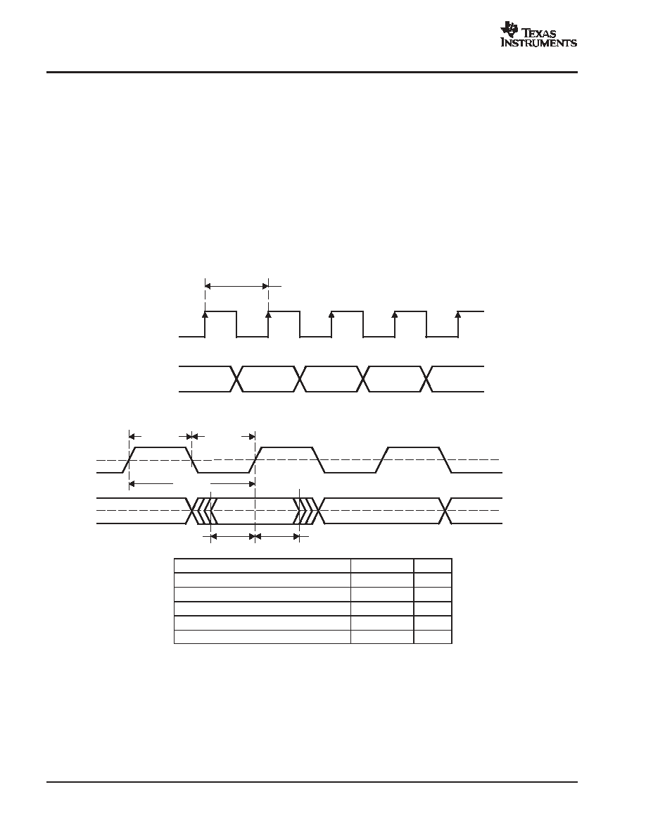
PCM1791A
SLES071A - MARCH 2003 - REVISED JANUARY 2004
www.ti.com
40
Pin Assignments When Using the DSD Format Interface
Several pins are redefined for DSD mode operation. These include:
D
DATA (pin 3): DSDL as L-channel DSD data input, or as DSD data input in mono mode
D
LRCK (pin 1): DSDR as R-channel DSD data input
D
SCK (pin 5): DBCK as bit clock for DSD data
D
BCK (pin 2): Set LOW (N/A)
Requirements for System Clock
The bit clock (DBCK) for DSD mode is required at pin 5 of the PCM1791A. The frequency of bit clock may be N times
the sampling frequency. Generally, N is 64 in DSD applications.
The interface timing between the bit clock and DSDL, DSDR is required to meet the setup and hold time specifications
shown in Figure 43.
t = 1/(64
×
44.1 kHz)
D1
DSDL
DSDR
D0
D2
D3
D4
DBCK
Figure 42. Normal Data Output Form From DSD Decoder
DSDL
DSDR
t(BCH)
DBCK
t(BCL)
t(BCY)
1.4 V
1.4 V
t(DS)
t(DH)
PARAMETER
MIN
MAX
UNITS
t(BCY) DBCK pulse cycle time
85(1)
ns
t(BCH) DBCK high-level time
30
ns
t(BCL) DBCK low-level time
30
ns
t(DS)
DSDL, DSDR setup time
10
ns
t(DH)
DSDL, DSDR hold time
10
ns
(1) 2.8224 MHz
×
4. (2.8224 MHz = 64
×
44.1 kHz. This value is specified as a
sampling rate of DSD.)
Figure 43. Timing for DSD Audio Interface
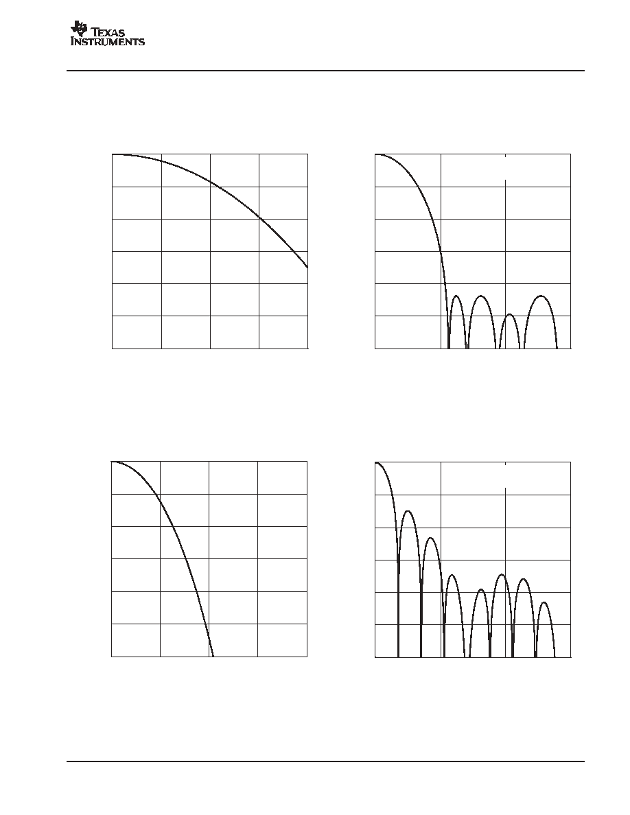
PCM1791A
SLES071A - MARCH 2003 - REVISED JANUARY 2004
www.ti.com
41
ANALOG FIR FILTER PERFORMANCE IN DSD MODE
Figure 44. DSD Filter-1, Low BW
f - Frequency - kHz
-6
-5
-4
-3
-2
-1
0
0
50
100
150
200
Gain - dB
GAIN
vs
FREQUENCY
Figure 45. DSD Filter-1, High BW
f - Frequency - kHz
-60
-50
-40
-30
-20
-10
0
0
500
1000
1500
Gain - dB
GAIN
vs
FREQUENCY
fc = 185 kHz
Gain(1) = -6.6 dB
Figure 46. DSD Filter-2, Low BW
f - Frequency - kHz
-6
-5
-4
-3
-2
-1
0
0
50
100
150
200
Gain - dB
GAIN
vs
FREQUENCY
Figure 47. DSD Filter-2, High BW
f - Frequency - kHz
-60
-50
-40
-30
-20
-10
0
0
500
1000
1500
Gain - dB
GAIN
vs
FREQUENCY
fc = 77 kHz
Gain (1) = -6 dB
(1) This gain is in comparison to PCM 0 dB, when the DSD input signal efficiency is 50%.
All specifications at DBCK = 2.8224 MHz (44.1 kHz
×
64 fS), and 50% modulation DSD data input, unless otherwise noted.
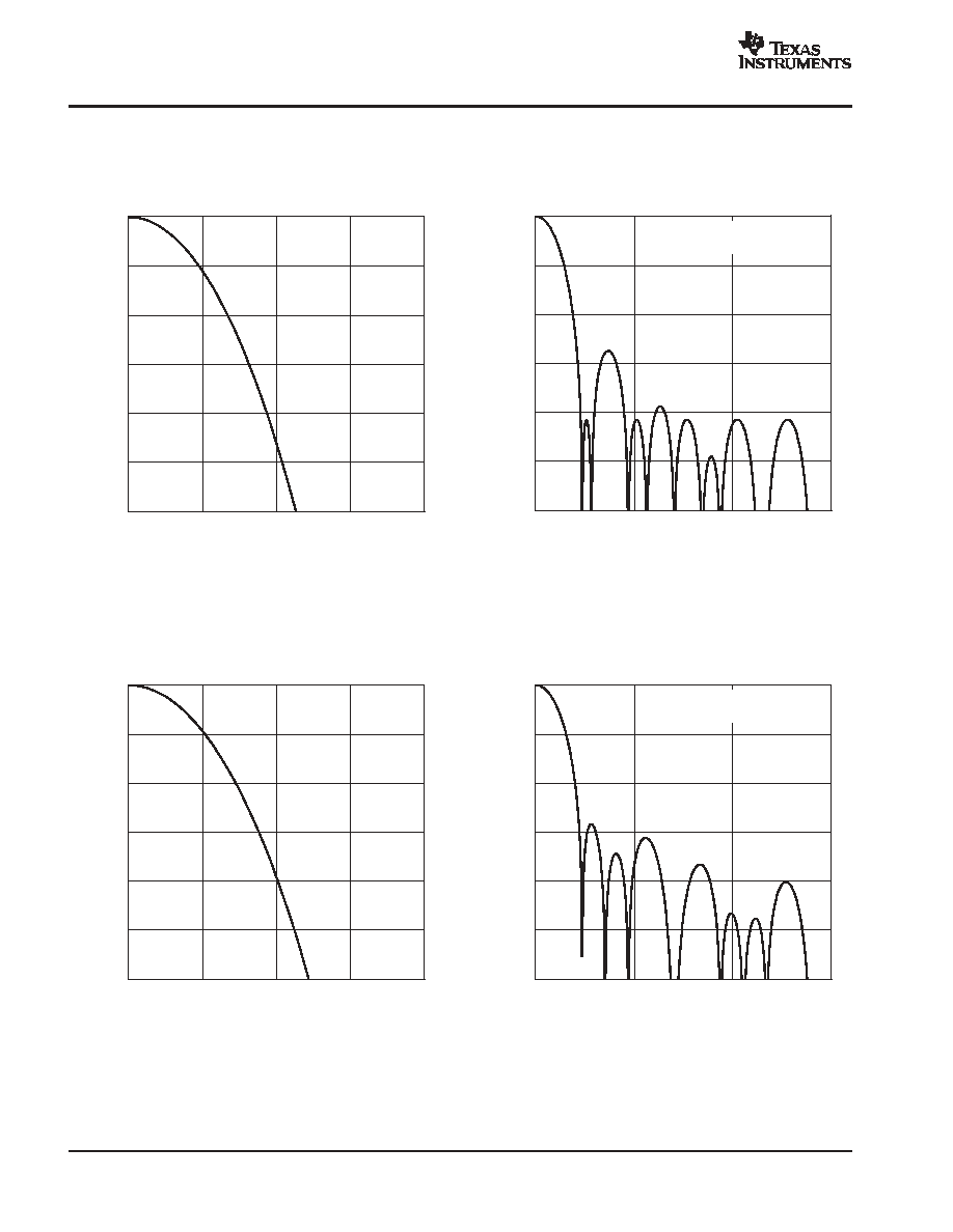
PCM1791A
SLES071A - MARCH 2003 - REVISED JANUARY 2004
www.ti.com
42
ANALOG FIR FILTER PERFORMANCE IN DSD MODE (CONTINUED)
Figure 48. DSD Filter-3, Low BW
f - Frequency - kHz
-6
-5
-4
-3
-2
-1
0
0
50
100
150
200
Gain - dB
GAIN
vs
FREQUENCY
Figure 49. DSD Filter-3, High BW
f - Frequency - kHz
-60
-50
-40
-30
-20
-10
0
0
500
1000
1500
Gain - dB
GAIN
vs
FREQUENCY
fc = 85 kHz
Gain(1) = -1.5 dB
Figure 50. DSD Filter-4, Low BW
f - Frequency - kHz
-6
-5
-4
-3
-2
-1
0
0
50
100
150
200
Gain - dB
GAIN
vs
FREQUENCY
Figure 51. DSD Filter-4, High BW
f - Frequency - kHz
-60
-50
-40
-30
-20
-10
0
0
500
1000
1500
Gain - dB
GAIN
vs
FREQUENCY
fc = 94 kHz
Gain(1) = -3.3 dB
(1) This gain is in comparison to PCM 0 dB, when the DSD input signal efficiency is 50%.
All specifications at DBCK = 2.8224 MHz (44.1 kHz
×
64 fS), and 50% modulation DSD data input, unless otherwise noted.
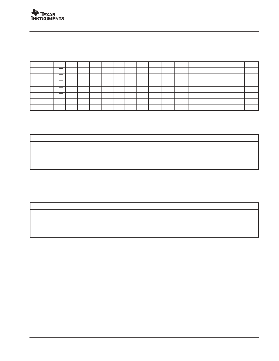
PCM1791A
SLES071A - MARCH 2003 - REVISED JANUARY 2004
www.ti.com
43
DSD MODE CONFIGURATION AND FUNCTION CONTROLS
Configuration for the DSD Interface Mode
DSD = 1 (Register 20, B5)
B15
B14
B13
B12
B11
B10
B9
B8
B7
B6
B5
B4
B3
B2
B1
B0
Register 16
R/W
0
0
1
0
0
0
0
-
-
-
-
-
-
-
-
Register 17
R/W
0
0
1
0
0
0
1
-
-
-
-
-
-
-
-
Register 18
R/W
0
0
1
0
0
1
0
-
-
-
-
DMF1
DMF0
-
-
Register 19
R/W
0
0
1
0
0
1
1
REV
-
-
OPE
-
-
-
-
Register 20
R/W
0
0
1
0
1
0
0
-
SRST
1
-
MONO
-
OS1
OS0
Register 21
R
0
0
1
0
1
0
1
-
-
-
-
-
DZ1
DZ0
-
Register 22
R
0
0
1
0
1
1
0
-
-
-
-
-
-
ZFGR
ZFGL
NOTE: -: Function is disabled. No operation even if data bit is set
DMF[1:0]: Analog FIR Performance Selection
Default value: 00
DMF[1:0]
Analog FIR Performance Select
00
FIR-1 (default)
01
FIR-2
10
FIR-3
11
FIR-4
Plots for the four analog FIR filter responses are shown in the ANALOG FIR FILTER PERFORMANCE IN DSD
MODE section of this data sheet.
OS[1:0]: Analog-FIR Operation Speed Selection
Default value: 00
OS[1:0]
Operation Speed Select
00
f
DBCK
(default)
01
f
DBCK
/2
10
Reserved
11
f
DBCK
/4
The OS bits in the DSD mode select the operating rate of the analog FIR. The OS bits must be set before setting
the DSD bit to 1.
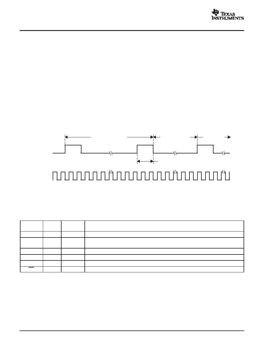
PCM1791A
SLES071A - MARCH 2003 - REVISED JANUARY 2004
www.ti.com
44
TDMCA INTERFACE FORMAT
The PCM1791A supports the time-division-multiplexed command and audio (TDMCA) data format to simplify the
host control serial interface. The TDMCA format is designed not only for the McBSP of TI DSPs but also for any
programmable devices. The TDMCA format can transfer not only audio data but also command data, so that it can
be used together with any kind of device that supports the TDMCA format. The TDMCA frame consists of a command
field, extended command field, and some audio data fields. Those audio data are transported to IN devices (such
as a DAC) and/or from OUT devices (such as an ADC). The PCM1791A is an IN device. LRCK and BCK are used
with both IN and OUT devices so that the sample frequency of all devices in a system must be the same. The TDMCA
mode supports a maximum of 30 device IDs. The maximum number of audio channels depends on the BCK
frequency.
TDMCA Mode Determination
The PCM1791A recognizes the TDMCA mode automatically when it receives an LRCK signal with a pulse duration
of two BCK clocks. If the TDMCA mode operation is not needed, the duty cycle of LRCK must be 50%. Figure 52
shows the LRCK and BCK timing that determines the TDMCA mode. The PCM1791A enters the TDMCA mode after
two continuous TDMCA frames. Any TDMCA commands can be issued during the next TDMCA frame after the
TDMCA mode is entered.
Pre-TDMCA Frame
BCK
LRCK
2 BCK
TDMCA Frame
Command
Accept
Figure 52. LRCK and BCK Timing for Determination of TDMCA Mode
TDMCA Terminals
TDMCA requires six signals, four of which are for command and audio data interface, and one pair of signals which
are for daisy chaining. Those signals can be shared as in the following table. The DO signal has a 3-state output so
that it can be connected directly to other devices.
TERMINAL
NAME
TDMCA
NAME
PROPERTY
DESCRIPTION
LRCK
LRCK
input
TDMCA frame start signal. It must be the same as the sampling frequency.
BCK
BCK
input
TDMCA clock. Its frequency must be high enough to communicate a TDMCA frame within an LRCK
cycle.
DATA
DI
input
TDMCA command and audio data input signal
MDI
DO
output
TDMCA command data 3-state output signal
MC
DCI
input
TDMCA daisy-chain input signal
MS
DCO
output
TDMCA daisy-chain output signal
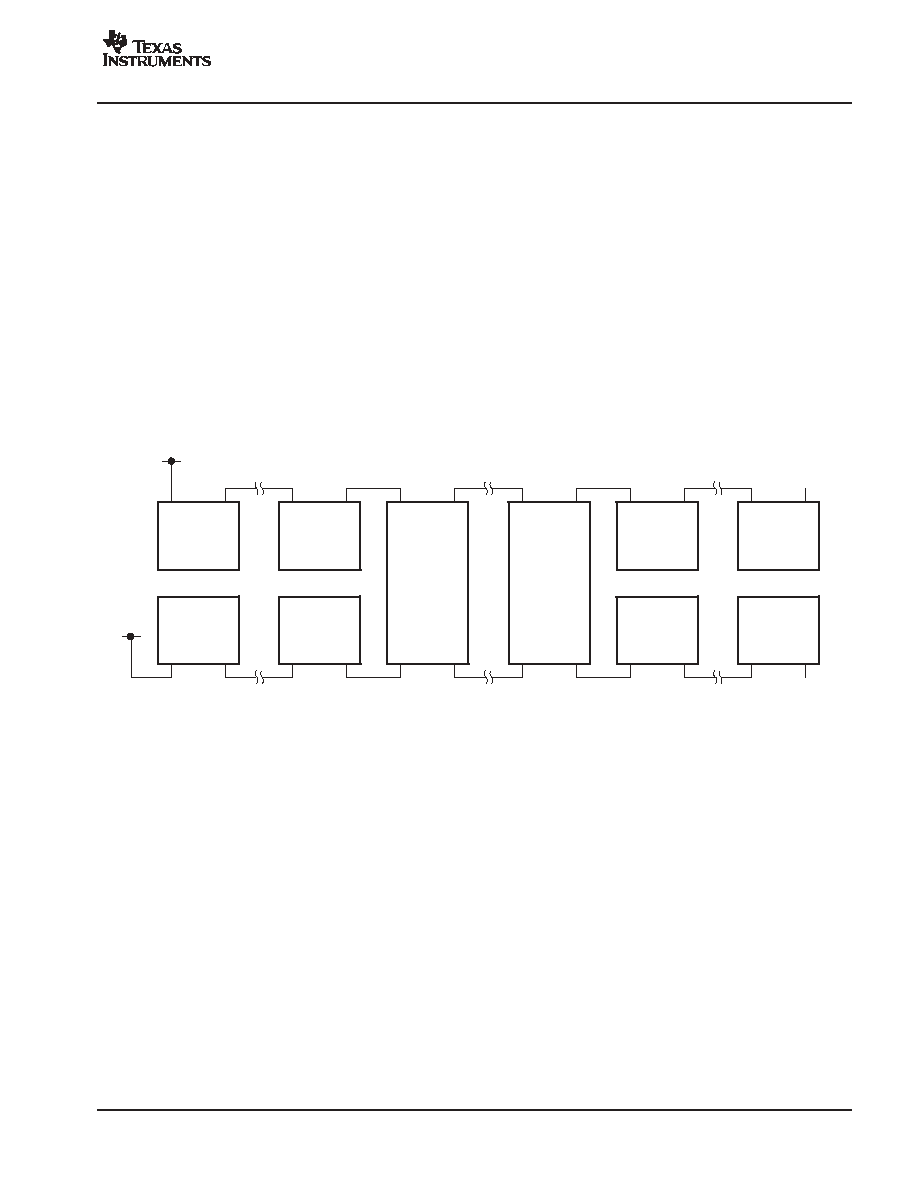
PCM1791A
SLES071A - MARCH 2003 - REVISED JANUARY 2004
www.ti.com
45
Device ID Determination
The TDMCA mode also supports a multichip implementation in one system. This means a host controller (DSP) can
simultaneously support several TDMCA devices, which can be of the same type or different types, including PCM
devices. The PCM devices are categorized as IN device, OUT device, IN/OUT device, and NO device. The IN device
has an input port to get audio data, the OUT device has an output port to supply audio data, the IN/OUT device has
both input and output ports for audio data, and the NO device has no port for audio data but needs command data
from the host. A DAC is an IN device, an ADC is an OUT device, a CODEC is an IN/OUT device, and a PLL is a NO
device. The PCM1791A is an IN device. For the host controller to distinguish the devices, each device is assigned
its own device ID by the daisy chain. The devices obtain their own device IDs automatically by connecting their DCI
to the DCO of the preceding device and their DCO to the DCI of the following device in the daisy chain. The daisy
chains are categorized as the IN chain and the OUT chain, which are completely independent and equivalent.
Figure 53 shows an example daisy chain connection. If a system needs to chain the PCM1791A and a NO device
in the same IN or OUT chain, the NO device must be chained at the back end of the chain because it does not require
any audio data. Figure 54 shows an example of TDMCA system including an IN chain and an OUT chain with a TI
DSP. For a device to get its own device ID, the DID signal must be set to 1 (see the Command Field section for details),
and LRCK and BCK must be driven in the TDMCA mode for all PCM devices which are chained. The device at the
top of the chain knows its device ID is 1 because its DCI is fixed HIGH. Other devices count the BCK pulses and
observe their own DCI signal to determine their position and ID. Figure 55 shows the initialization of each device ID.
IN Device
DCI
DCO
OUT Device
DCI
DCO
IN
OUT
IN/OUT
IN Chain
OUT Chain
IN Device
OUT Device
DCI
DCO
DCI
DCO
DCIi
DCIo
DCOi
DCOo
IN
OUT
DCIi
DCIo
DCOi
DCOo
NO Device
DCI
DCO
NO Device
DCI
DCO
NO Device
NO Device
DCI
DCO
DCI
DCO
Device
IN/OUT
Device
·
·
·
·
·
·
·
·
·
·
·
·
·
·
·
Figure 53. Daisy Chain Connection
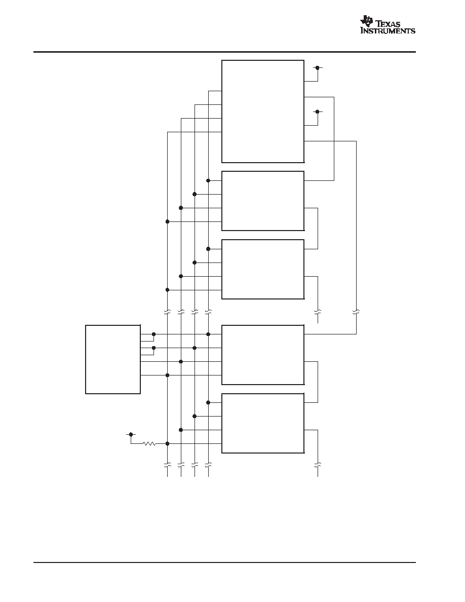
PCM1791A
SLES071A - MARCH 2003 - REVISED JANUARY 2004
www.ti.com
46
IN Device
(PCM1791A)
DCI
DCO
LRCK
BCK
DI
DO
Device ID = 2
TI DSP
FSX
CLKX
DX
FSR
CLKR
DR
NO Device
DCI
DCO
OUT Device
DCI
DCO
OUT Device
DCI
DCO
Device ID = 3
Device ID = 2
Device ID = 3
LRCK
BCK
DI
DO
LRCK
BCK
DI
DO
LRCK
BCK
DI
DO
IN/OUT
Device
DCII
DCIO
LRCK
BCK
DI
DO
Device ID = 1
DCOO
DCOI
·
·
·
·
·
·
(DIX1700)
Figure 54. IN Daisy Chain and OUT Daisy Chain Connection for a Multichip System
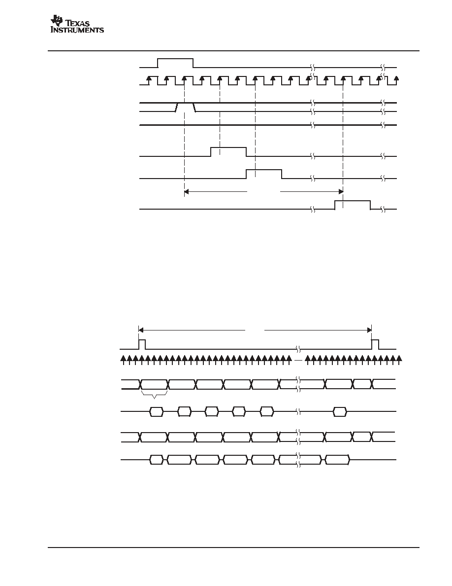
PCM1791A
SLES071A - MARCH 2003 - REVISED JANUARY 2004
www.ti.com
47
58 BCK
Command Field
DID
LRCK
BCK
DI
DCO1
DCI2
Device ID = 1
Device ID = 2
DCO1
DCO2
DCI3
DCO29
DCI30
Device ID = 3
Device ID = 30
·
·
·
·
·
·
Figure 55. Device ID Determination Sequence
TDMCA Frame
In general, the TDMCA frame consists of the command field, extended command (EMD) field, and audio data fields.
All of them are 32 bits in length, but the lowest byte has no meaning. The MSB is transferred first for each field. The
command field is always transferred as the first packet of the frame. The EMD field is transferred if the EMD flag of
the command field is HIGH. If any EMD packets are transferred, no audio data follows the EMD packets. This frame
is for quick system initialization. All devices of a daisy chain should respond to the command field and extended
command field. The PCM1791A has two audio channels that can be selected by OPE (register 19). If this OPE bit
is not set to HIGH, those audio channels are transferred. Figure 56 shows the general TDMCA frame. If some DACs
are enabled, but corresponding audio data packets are not transferred, the analog outputs are unpredictable.
LRCK
BCK
DI
CMD
EMD
EMD
EMD
CMD
Don't
Care
EMD
EMD
DO
Ch1
Ch(m)
Ch2
CMD
CMD
Ch2
Ch3
Ch(n)
CMD
Ch1
Ch4
DI
Ch3
Ch4
[For Initialization]
[For Operation]
32 Bits
DO
CMD
CMD
CMD
CMD
CMD
CMD
1/fS
Don't
Care
Figure 56. General TDMCA Frame
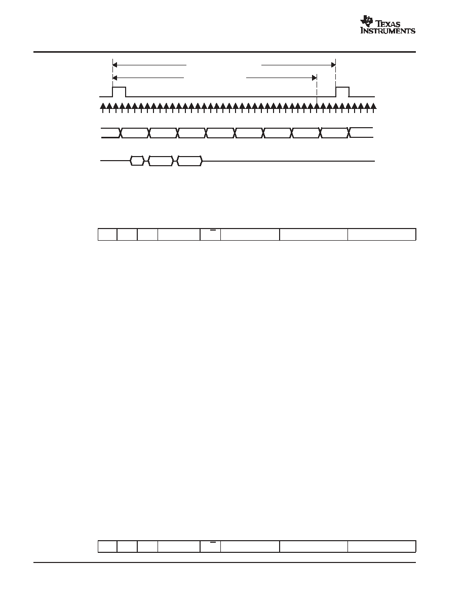
PCM1791A
SLES071A - MARCH 2003 - REVISED JANUARY 2004
www.ti.com
48
BCK
DI
CMD
Don't
Care
Ch1
CMD
CMD
Ch2
Ch3
Ch1
Ch4
IN and OUT Channel Orders are Completely Independent
DO
7 Packets
×
32 Bits
Ch5
Ch6
1/fS (256 BCK Clocks)
Ch2
LRCK
Figure 57. TDMCA Frame Example of 6-Ch DAC and 2-Ch ADC With Command Read
Command Field
The normal command field is defined as follows. When the DID bit (MSB) is 1, this frame is used only for device ID
determination, and all remaining bits in the field are ignored.
31
30
29
28 24
23
22 16
15 8
7 0
command
DID
EMD
DCS
device ID
R/W
register ID
data
not used
Bit 31: Device ID enable flag
The PCM1791A operates to get its own device ID for TDMCA initialization if this bit is HIGH.
Bit 30: Extended command enable flag
An EMD packet is transferred if this bit is HIGH, otherwise skipped. Once it is HIGH, this frame does not contain any
audio data. This is for system initialization.
Bit 29: Daisy chain selection flag
HIGH designates OUT-chain devices, LOW designates IN-chain devices. The PCM1791A is an IN device, so the
DCS bit must be set to LOW.
Bits[28:24]: Device ID
The device ID is 5 bits in length, and it can be defined. These bits identify the order of a device in the IN or OUT daisy
chain. The top of the daisy chain defines device ID 1 and successive devices are numbered 2, 3, 4, etc. All devices
for which the DCI is fixed HIGH are also defined as ID 1. The maximum device ID is 30 each in the IN and OUT chains.
If a device ID of 0x1F is used, all devices are selected as broadcast when in the write mode. If a device ID of 0x00
is used, no device is selected.
Bit 23: Command Read/Write flag
If this bit is HIGH, the command is a read operation.
Bits[22:16]: Register ID
It is 7 bits in length.
Bits[15:8]: Command data
It is 8 bits in length. Any valid data can be chosen for each register.
Bits[7:0]: Not used
These bits are never transported when a read operation is performed.
Extended command field
The extended command field is the same as the command field, except that it does not have a DID flag.
31
30
29
28 24
23
22 16
15 8
7 0
extended command
rsvd
EMD
DCS
device ID
R/W
register ID
data
not used
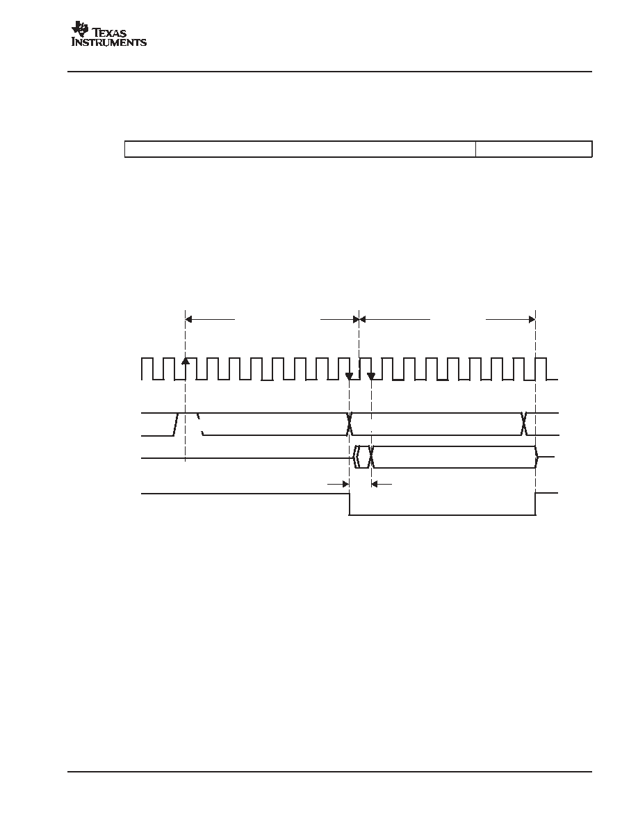
PCM1791A
SLES071A - MARCH 2003 - REVISED JANUARY 2004
www.ti.com
49
Audio Fields
The audio field is 32 bits in length and the audio data is transferred MSB first, so the other fields must be stuffed with
0s as shown in the following example.
31 16 12 8
7 4 3 0
audio data
MSB 24 bits LSB
All 0s
TDMCA Register Requirements
TDMCA mode requires device ID and audio channel information, previously described. The OPE bit in register 19
indicates audio channel availability and register 23 indicates the device ID. Register 23 is used only in the TDMCA
mode. See the mode control register map (Table 4).
Register Write/Read Operation
The command supports register write and read operations. If the command requests to read one register, the read
data is transferred on DO during the data phase of the timing cycle. The DI signal can be retrieved at the positive
edge of BCK, and the DO signal is driven at the negative edge of BCK. DO is activated one BCK cycle early to
compensate for the output delay caused by high impedance. Figure 58 shows the TDMCA write and read timing.
BCK
DI
DO
DOEN
(Internal)
1 BCK Early
Read Mode and Proper Register ID
Write Data Retrieved, if Write Mode
Read Data Driven, if Read Mode
Register ID Phase
Data Phase
Figure 58. TDMCA Write and Read Operation Timing
TDMCA-Mode Operation
DCO specifies the owner of the next audio channel in TDMCA-mode operation. When a device retrieves its own audio
channel data, DCO goes HIGH during the last audio channel period. Figure 59 shows the DCO output timing in
TDMCA-mode operation. The host controller ignores the behavior of DCI and DCO. DCO indicates the last audio
channel of each device. Therefore, DCI means the next audio channel is allocated.
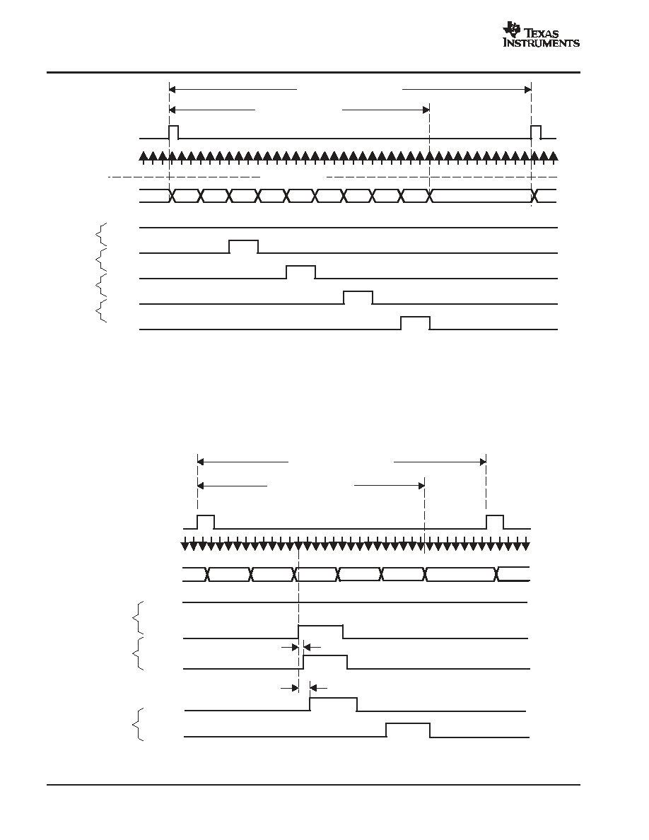
PCM1791A
SLES071A - MARCH 2003 - REVISED JANUARY 2004
www.ti.com
50
9 Packets
×
32 Bits
LRCK
BCK
DI
CMD
Don't Care
DCI1
DCO1
DID = 1
DCI2
DCO2
DID = 2
DCI3
DCO3
DID = 3
DCI4
DCO4
DID = 4
IN Daisy Chain
CMD
Ch1
Ch2
Ch3
Ch4
Ch5
Ch6
Ch7
Ch8
1/fS (384 BCK Clocks)
Figure 59. DCO Output Timing of TDMCA Mode Operation
If some devices are skipped due to no active audio channel, the skipped devices must notify the next device that the
DCO will be passed through the next DCI. Figure 60 and Figure 61 show DCO timing with skip operation. Figure 62
shows the ac timing of the daisy chain signals.
DID = 1
DID = 2
DID = 8
Don't Care
DCI
DCO
DCI
DCO
DCI
DCO
LRCK
BCK
DI
CMD
Ch1
Ch16
CMD
Ch2
Ch15
14 BCK Delay
2 BCK Delay
5 Packets
×
32 Bits
1/fS (256 BCK Clocks)
·
·
·
·
·
·
·
·
·
Figure 60. DCO Output Timing With Skip Operation
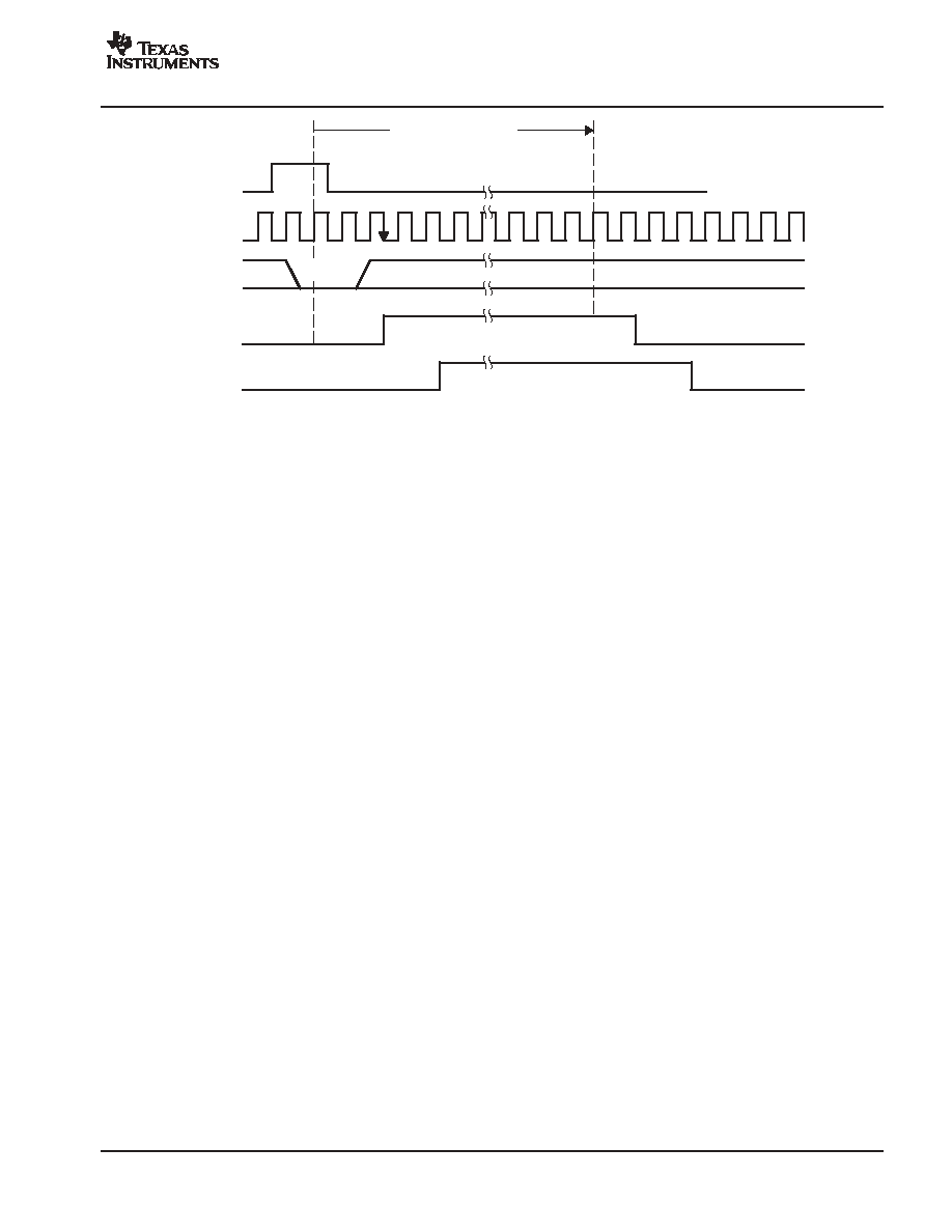
PCM1791A
SLES071A - MARCH 2003 - REVISED JANUARY 2004
www.ti.com
51
·
·
·
Command Packet
LRCK
BCK
DI
DCO1
DCO2
DID EMD
Figure 61. DCO Output Timing With Skip Operation (for Command Packet 1)
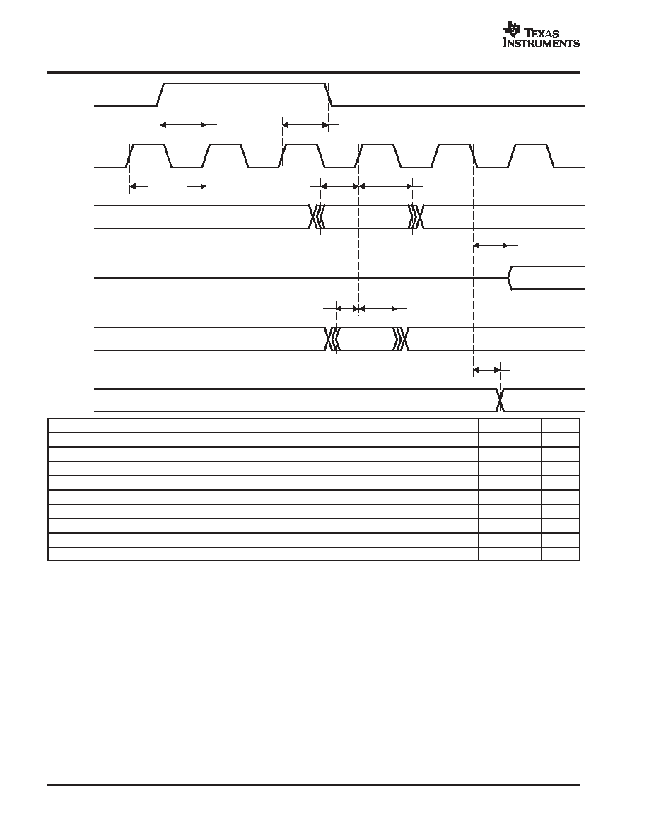
PCM1791A
SLES071A - MARCH 2003 - REVISED JANUARY 2004
www.ti.com
52
t(DS)
t(COE)
BCK
LRCK
DI
DCI
DO
DCO
t(DH)
t(DOE)
t(DH)
t(DS)
t(BL)
t(LB)
t(BCY)
PARAMETER
MIN
MAX
UNITS
t(BCY) BCK pulse cycle time
20
ns
t(LB)
LRCK setup time
0
ns
t(BL)
LRCK hold time
3
ns
t(DS)
DI setup time
0
ns
t(DH)
DI hold time
3
ns
t(DS)
DCI setup time
0
ns
t(DH)
DCI hold time
3
ns
t(DOE) DO output delay(1)
8
ns
t(COE) DCO output delay(1)
6
ns
(1) Load capacitance is 10 pF.
Figure 62. AC Timing of Daisy Chain Signals
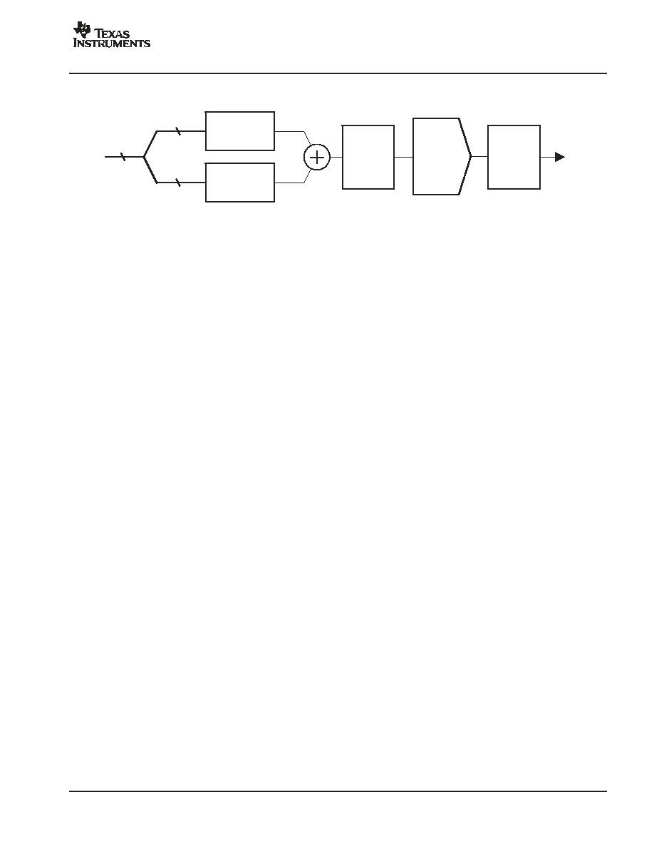
PCM1791A
SLES071A - MARCH 2003 - REVISED JANUARY 2004
www.ti.com
53
THEORY OF OPERATION
Analog
Voltage
Output
Digital
Input
24 Bit
8 fS
MSB
and
Lower 18 Bit
Upper
6 Bit
ICOB
Decoder
3rd-Order
5-Level
Sigma-Delta
Advanced
DWA
Current
Segment
DAC
0-4
Level
0-62
Level
0-66
I/V
Converter
Figure 63. Advanced Segment DAC With I/V Converter
The PCM1791A uses TI's advanced segment DAC architecture to achieve excellent dynamic performance and
improved tolerance to clock jitter. The PCM1791A provides balanced voltage outputs.
Digital input data via the digital filter is separated into 6 upper bits and 18 lower bits. The 6 upper bits are converted
to inverted complementary offset binary (ICOB) code. The lower 18 bits, in association with the MSB, are processed
by a five-level third-order delta-sigma modulator operated at 64 f
S
by default. The 1 level of the modulator is equivalent
to the 1 LSB of the ICOB code converter. The data groups processed in the ICOB converter and third-order
delta-sigma modulator are summed together to an up to 66-level digital code, and then processed by data-weighted
averaging (DWA) to reduce the noise produced by element mismatch. The data of up to 66 levels from the DWA is
converted to an analog output in the differential-current segment section.
This architecture has overcome the various drawbacks of conventional multibit processing and also achieves
excellent dynamic performance.
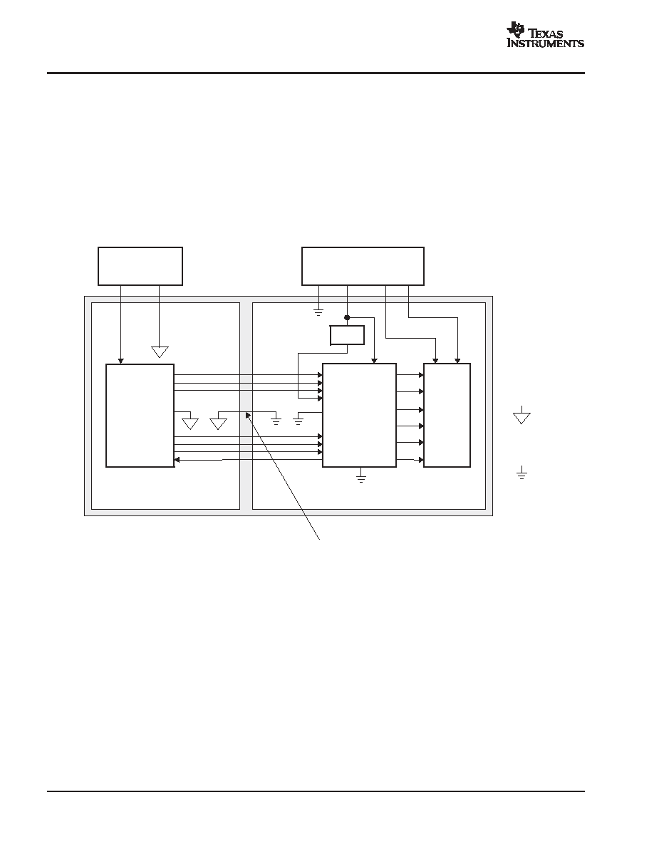
PCM1791A
SLES071A - MARCH 2003 - REVISED JANUARY 2004
www.ti.com
54
CONSIDERATIONS FOR APPLICATION CIRCUITS
PCB Layout Guidelines
A typical PCB floor plan for the PCM1791A is shown in Figure 64. A ground plane is recommended, with the analog
and digital sections being isolated from one another using a split or cut in the circuit board. The PCM1791A must
be oriented with the digital I/O pins facing the ground plane split/cut to allow for short, direct connections to the digital
audio interface and control signals originating from the digital section of the board. Separate power supplies are
recommended for the digital and analog sections of the board. This prevents the switching noise present on the digital
supply from contaminating the analog power supply and degrading the dynamic performance of the D/A converters.
In cases where a common 5-V supply would be used for the analog and digital sections, an inductance (RF choke,
ferrite bead) must be placed between the analog and digital 5-V supply connections to avoid coupling of the digital
switching noise into the analog circuitry. Figure 65 shows the recommended approach for single-supply applications.
Digital Logic
and
Audio
Processor
Digital Power
+VD
DGND
Digital Section
Analog Section
Return Path for Digital Signals
Analog Power
+VS
AGND
-VS
+5VA
Digital
Ground
Analog
Ground
Output
Circuits
PCM1791A
AGND
VCC
VDD
DGND
REG
Figure 64. Recommended PCB Layout
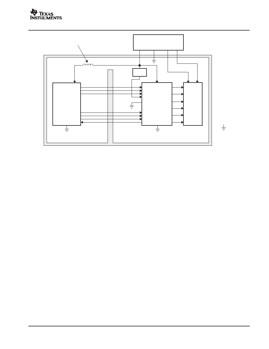
PCM1791A
SLES071A - MARCH 2003 - REVISED JANUARY 2004
www.ti.com
55
VDD
Digital Section
Analog Section
RF Choke or Ferrite Bead
Power Supplies
Common
Ground
Output
Circuits
AGND
VCC
+VS
+5V
-VS
AGND
VDD
DGND
REG
PCM1791A
Figure 65. Single-Supply PCB Layout
Bypass and Decoupling Capacitor Requirements
Various sized decoupling capacitors can be used, with no special tolerances being required. All capacitors must be
located as close as possible to the appropriate pins of the PCM1791A to reduce noise pickup from surrounding
circuitry. Aluminum electrolytic capacitors that are designed for hi-fi audio applications are recommended for larger
values, while metal film or monolithic ceramic capacitors are used for smaller values.
Post-LPF Design
By proper choice of the op amp and resistors used in the post-LPF circuit, excellent performance of the PCM1791A
should be achieved. To obtain 0.001% THD+N and 113 dB signal-to-noise-ratio audio performance, the THD+N and
input noise performance of the op amp should be considered. This is because the input noise of the op amp
contributes directly to the output noise level of the application. The V
OUT
pin of the PCM1791A and the input resistor
of the post-LPF circuit must be connected as closely as possible.
Out-of-band noise level and attenuated sampling spectrum level are much lower than for typical delta-sigma type
DACs due to the combination of a high-performance digital filter and advanced segment DAC architecture. The use
of a second-order or third-order post-LPF is recommended for the post-LPF of the PCM1791A. The cutoff frequency
of the post-LPF depends on the application. For example, there are many sampling-rate operations such as f
S
= 44.1
kHz on CDDA, f
S
= 96 kHz on DVD-M, f
S
= 192 kHz on DVD-A, f
S
= 64 f
S
on DSD (SACD).
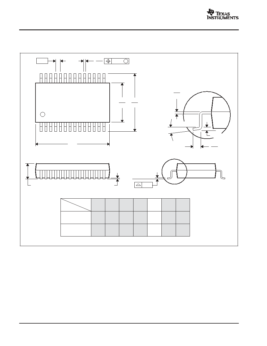
PCM1791A
SLES071A - MARCH 2003 - REVISED JANUARY 2004
www.ti.com
56
MECHANICAL DATA
DB (R-PDSO-G**)
PLASTIC SMALL-OUTLINE
4040065 /E 12/01
28 PINS SHOWN
Gage Plane
8,20
7,40
0,55
0,95
0,25
38
12,90
12,30
28
10,50
24
8,50
Seating Plane
9,90
7,90
30
10,50
9,90
0,38
5,60
5,00
15
0,22
14
A
28
1
20
16
6,50
6,50
14
0,05 MIN
5,90
5,90
DIM
A MAX
A MIN
PINS **
2,00 MAX
6,90
7,50
0,65
M
0,15
0
°
-8
°
0,10
0,09
0,25
NOTES: A. All linear dimensions are in millimeters.
B. This drawing is subject to change without notice.
C. Body dimensions do not include mold flash or protrusion not to exceed 0,15.
D. Falls within JEDEC MO-150
PACKAGING INFORMATION
Orderable Device
Status
(1)
Package
Type
Package
Drawing
Pins Package
Qty
Eco Plan
(2)
Lead/Ball Finish
MSL Peak Temp
(3)
PCM1791ADB
ACTIVE
SSOP
DB
28
47
Pb-Free
(RoHS)
CU NIPDAU
Level-1-260C-UNLIM
PCM1791ADBR
ACTIVE
SSOP
DB
28
2000
None
CU SNBI
Level-1-235C-UNLIM
(1)
The marketing status values are defined as follows:
ACTIVE: Product device recommended for new designs.
LIFEBUY: TI has announced that the device will be discontinued, and a lifetime-buy period is in effect.
NRND: Not recommended for new designs. Device is in production to support existing customers, but TI does not recommend using this part in
a new design.
PREVIEW: Device has been announced but is not in production. Samples may or may not be available.
OBSOLETE: TI has discontinued the production of the device.
(2)
Eco Plan - May not be currently available - please check
http://www.ti.com/productcontent
for the latest availability information and additional
product content details.
None: Not yet available Lead (Pb-Free).
Pb-Free (RoHS): TI's terms "Lead-Free" or "Pb-Free" mean semiconductor products that are compatible with the current RoHS requirements
for all 6 substances, including the requirement that lead not exceed 0.1% by weight in homogeneous materials. Where designed to be soldered
at high temperatures, TI Pb-Free products are suitable for use in specified lead-free processes.
Green (RoHS & no Sb/Br): TI defines "Green" to mean "Pb-Free" and in addition, uses package materials that do not contain halogens,
including bromine (Br) or antimony (Sb) above 0.1% of total product weight.
(3)
MSL, Peak Temp. -- The Moisture Sensitivity Level rating according to the JEDECindustry standard classifications, and peak solder
temperature.
Important Information and Disclaimer:The information provided on this page represents TI's knowledge and belief as of the date that it is
provided. TI bases its knowledge and belief on information provided by third parties, and makes no representation or warranty as to the
accuracy of such information. Efforts are underway to better integrate information from third parties. TI has taken and continues to take
reasonable steps to provide representative and accurate information but may not have conducted destructive testing or chemical analysis on
incoming materials and chemicals. TI and TI suppliers consider certain information to be proprietary, and thus CAS numbers and other limited
information may not be available for release.
In no event shall TI's liability arising out of such information exceed the total purchase price of the TI part(s) at issue in this document sold by TI
to Customer on an annual basis.
PACKAGE OPTION ADDENDUM
www.ti.com
4-Mar-2005
Addendum-Page 1

IMPORTANT NOTICE
Texas Instruments Incorporated and its subsidiaries (TI) reserve the right to make corrections, modifications,
enhancements, improvements, and other changes to its products and services at any time and to discontinue
any product or service without notice. Customers should obtain the latest relevant information before placing
orders and should verify that such information is current and complete. All products are sold subject to TI's terms
and conditions of sale supplied at the time of order acknowledgment.
TI warrants performance of its hardware products to the specifications applicable at the time of sale in
accordance with TI's standard warranty. Testing and other quality control techniques are used to the extent TI
deems necessary to support this warranty. Except where mandated by government requirements, testing of all
parameters of each product is not necessarily performed.
TI assumes no liability for applications assistance or customer product design. Customers are responsible for
their products and applications using TI components. To minimize the risks associated with customer products
and applications, customers should provide adequate design and operating safeguards.
TI does not warrant or represent that any license, either express or implied, is granted under any TI patent right,
copyright, mask work right, or other TI intellectual property right relating to any combination, machine, or process
in which TI products or services are used. Information published by TI regarding third-party products or services
does not constitute a license from TI to use such products or services or a warranty or endorsement thereof.
Use of such information may require a license from a third party under the patents or other intellectual property
of the third party, or a license from TI under the patents or other intellectual property of TI.
Reproduction of information in TI data books or data sheets is permissible only if reproduction is without
alteration and is accompanied by all associated warranties, conditions, limitations, and notices. Reproduction
of this information with alteration is an unfair and deceptive business practice. TI is not responsible or liable for
such altered documentation.
Resale of TI products or services with statements different from or beyond the parameters stated by TI for that
product or service voids all express and any implied warranties for the associated TI product or service and
is an unfair and deceptive business practice. TI is not responsible or liable for any such statements.
Following are URLs where you can obtain information on other Texas Instruments products and application
solutions:
Products
Applications
Amplifiers
amplifier.ti.com
Audio
www.ti.com/audio
Data Converters
dataconverter.ti.com
Automotive
www.ti.com/automotive
DSP
dsp.ti.com
Broadband
www.ti.com/broadband
Interface
interface.ti.com
Digital Control
www.ti.com/digitalcontrol
Logic
logic.ti.com
Military
www.ti.com/military
Power Mgmt
power.ti.com
Optical Networking
www.ti.com/opticalnetwork
Microcontrollers
microcontroller.ti.com
Security
www.ti.com/security
Telephony
www.ti.com/telephony
Video & Imaging
www.ti.com/video
Wireless
www.ti.com/wireless
Mailing Address:
Texas Instruments
Post Office Box 655303 Dallas, Texas 75265
Copyright
2005, Texas Instruments Incorporated