 | –≠–ª–µ–∫—Ç—Ä–æ–Ω–Ω—ã–π –∫–æ–º–ø–æ–Ω–µ–Ω—Ç: PCM1793 | –°–∫–∞—á–∞—Ç—å:  PDF PDF  ZIP ZIP |
PCM1793
SLES076A - MARCH 2003 - REVISED JANUARY 2004
24 BIT, 192 kHz SAMPLING, ADVANCED SEGMENT,
AUDIO STEREO DIGITAL TO ANALOG CONVERTER
FEATURES
D
24-Bit Resolution
D
Analog Performance:
- Dynamic Range: 113 dB
- THD+N: 0.001%
- Full-Scale Output: 2.1 V rms (at
Postamplifier)
D
Differential Voltage Output: 3.2 V p-p
D
8
◊
Oversampling Digital Filter:
- Stop-Band Attenuation: ≠82 dB
- Pass-Band Ripple:
±
0.002 dB
D
Sampling Frequency: 10 kHz to 200 kHz
D
System Clock: 128, 192, 256, 384, 512, or
768 f
S
With Autodetect
D
Accepts 16-, 20-, and 24-Bit Audio Data
D
Data Formats: Standard, I
2
S, and
Left-Justified
D
Digital De-Emphasis
D
Soft Mute
D
Zero Flags for Each Output
D
Dual Supply Operation:
- 5-V Analog, 3.3-V Digital
D
5-V Tolerant Digital Inputs
D
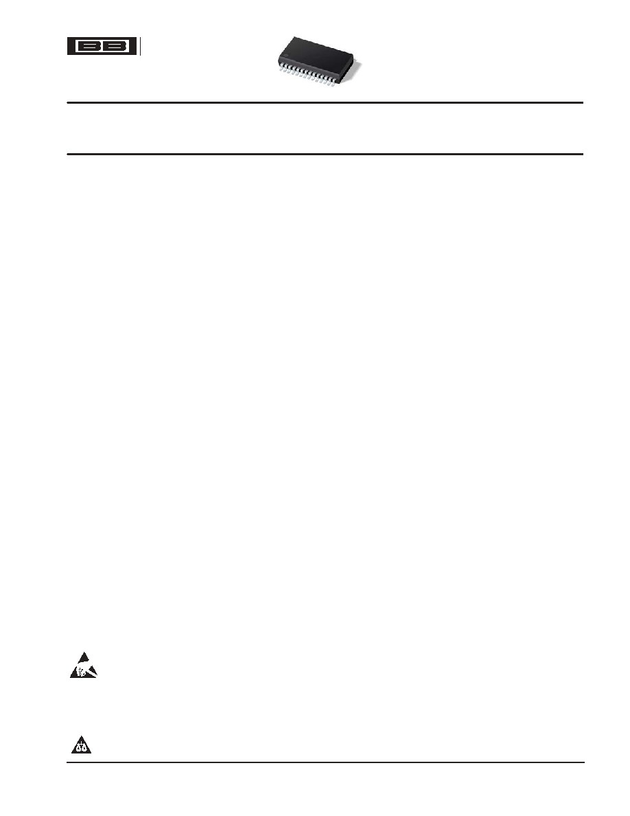
Small 28-Lead SSOP Package, Lead-Free
Product
APPLICATIONS
D
A/V Receivers
D
DVD Players
D
Musical Instruments
D
HDTV Receivers
D
Car Audio Systems
D
Digital Multitrack Recorders
D
Other Applications Requiring 24-Bit Audio
DESCRIPTION
The PCM1793 is a monolithic CMOS integrated circuit that
includes stereo digital-to-analog converters and support
circuitry in a small 28-lead SSOP package. The data
converters use TI's advanced segment DAC architecture
to achieve excellent dynamic performance and improved
tolerance to clock jitter. The PCM1793 provides balanced
voltage outputs, allowing the user to optimize analog
performance externally. Sampling rates up to 200 kHz are
supported.
This integrated circuit can be damaged by ESD. Texas Instruments recommends that all integrated circuits be handled with appropriate
precautions. Failure to observe proper handling and installation procedures can cause damage.
ESD damage can range from subtle performance degradation to complete device failure. Precision integrated circuits may be more susceptible to
damage because very small parametric changes could cause the device not to meet its published specifications.
PRODUCTION DATA information is current as of publication date. Products
conform to specifications per the terms of Texas Instruments standard warranty.
Production processing does not necessarily include testing of all parameters.
Please be aware that an important notice concerning availability, standard warranty, and use in critical applications of Texas Instruments
semiconductor products and disclaimers thereto appears at the end of this data sheet.
Burr Brown Products
from Texas Instruments
Copyright
2004, Texas Instruments Incorporated
PCM1793
SLES076A - MARCH 2003 - REVISED JANUARY 2004
www.ti.com
2
ORDERING INFORMATION
PRODUCT
PACKAGE
PACKAGE CODE
OPERATION
TEMPERATURE
RANGE
PACKAGE
MARKING
ORDERING
NUMBER
TRANSPORT
MEDIA
PCM1793DB
28-lead SSOP
28DB
-25
∞
C to 85
∞
C
PCM1793
PCM1793DB
Tube
PCM1793DB
28-lead SSOP
28DB
-25
∞
C to 85
∞
C
PCM1793
PCM1793DBR
Tape and reel
ABSOLUTE MAXIMUM RATINGS
over operating free-air temperature range unless otherwise noted(1)
PCM1793
Supply voltage
VCCF, VCCL, VCCC, VCCR
-0.3 V to 6.5 V
Supply voltage
VDD
-0.3 V to 4 V
Supply voltage differences: VCCF, VCCL, VCCC, VCCR
±
0.1 V
Ground voltage differences: AGNDF, AGNDL, AGNDC, AGNDR, DGND
±
0.1 V
Digital input voltage
LRCK, DATA, BCK, SCK, DEMP0, DEMP1, FMT0, FMT1, FMT2, RST, MUTE
≠0.3 V to 6.5 V
Digital input voltage
ZEROL, ZEROR
≠0.3 V to (VDD + 0.3 V) < 4 V
Analog input voltage
≠0.3 V to (VCC + 0.3 V) < 6.5 V
Input current (any pins except supplies)
±
10 mA
Ambient temperature under bias
≠40
∞
C to 125
∞
C
Storage temperature
≠55
∞
C to 150
∞
C
Junction temperature
150
∞
C
Lead temperature (soldering)
260
∞
C, 5 s
Package temperature (IR reflow, peak)
260
∞
C
(1) Stresses beyond those listed under "absolute maximum ratings" may cause permanent damage to the device. These are stress ratings only, and
functional operation of the device at these or any other conditions beyond those indicated under "recommended operating conditions" is not
implied. Exposure to absolute-maximum-rated conditions for extended periods may affect device reliability.
ELECTRICAL CHARACTERISTICS
all specifications at TA = 25
∞
C, VCC = 5 V, VDD = 3.3 V, fS = 44.1 kHz, system clock = 256 fS, and 24-bit data, unless otherwise noted
PARAMETER
TEST CONDITIONS
PCM1793DB
UNIT
PARAMETER
TEST CONDITIONS
MIN
TYP
MAX
UNIT
RESOLUTION
24
Bits
DATA FORMAT
Audio data interface format
Standard, I2S, left justified
Audio data bit length
16-, 20-, 24-bit selectable
Audio data format
MSB first, 2s complement
fS
Sampling frequency
10
200
kHz
System clock frequency
128, 192, 256, 384, 512, 768 fS
DIGITAL INPUT/OUTPUT
Logic family
TTL compatible
VIH
Input logic level
2
VDC
VIL
Input logic level
0.8
VDC
IIH
Input logic current
VIN = VDD
10
µ
A
IIL
Input logic current
VIN = 0 V
≠10
µ
A
VOH
Output logic level
IOH = -2 mA
2.4
VDC
VOL
Output logic level
IOL = 2 mA
0.4
VDC
PCM1793
SLES076A - MARCH 2003 - REVISED JANUARY 2004
www.ti.com
3
ELECTRICAL CHARACTERISTICS (Continued)
all specifications at TA = 25
∞
C, VCC = 5 V, VDD = 3.3 V, fS = 44.1 kHz, system clock = 256 fS, and 24-bit data, unless otherwise noted
PARAMETER
TEST CONDITIONS
PCM1793DB
UNIT
PARAMETER
TEST CONDITIONS
MIN
TYP
MAX
UNIT
DYNAMIC PERFORMANCE (1)
fS = 44.1 kHz
0.001%
0.002%
THD+N at VOUT = 0 dB
fS = 96 kHz
0.0015%
THD+N at VOUT = 0 dB
fS = 192 kHz
0.003%
EIAJ, A-weighted, fS = 44.1 kHz
110
113
Dynamic range
EIAJ, A-weighted, fS = 96 kHz
113
dB
Dynamic range
EIAJ, A-weighted, fS = 192 kHz
113
dB
EIAJ, A-weighted, fS = 44.1 kHz
110
113
Signal-to-noise ratio
EIAJ, A-weighted, fS = 96 kHz
113
dB
Signal-to-noise ratio
EIAJ, A-weighted, fS = 192 kHz
113
dB
fS = 44.1 kHz
106
110
Channel separation
fS = 96 kHz
110
dB
Channel separation
fS = 192 kHz
109
dB
Level linearity error
VOUT = -120 dB
±
1
dB
ANALOG OUTPUT
Gain error
≠8
±
3
8
% of FSR
Gain mismatch, channel-to-channel
≠3
±
0.5
3
% of FSR
Bipolar zero error
At BPZ
≠2
±
0.5
2
% of FSR
Differential output voltage (2)
Full scale (0 dB)
3.2
V p-p
Bipolar zero voltage (2)
At BPZ
1.4
V
Load impedance (2)
R1 = R2
1.7
k
DIGITAL FILTER PERFORMANCE
De-emphasis error
±
0.1
dB
Pass band
±
0.002 dB
0.454 fS
Pass band
≠3 dB
0.49 fS
Stop band
0.546 fS
Pass-band ripple
±
0.002
dB
Stop-band attenuation
Stop band = 0.546 fS
≠75
dB
Stop-band attenuation
Stop band = 0.567 fS
≠82
dB
Delay time
29/fS
s
(1) Dynamic performance and DC accuracy are specified at the output of the postamplifier as shown in Figure 28. Analog performance specifications
are measured using the System Two
t
Cascade audio measurement system by Audio Precision
t
in the averaging mode. At all sampling
frequency operations, measurement bandwidth is limited with a 20-kHz AES17 filter.
(2) These parameters are defined at the PCM1793 output pin. Load impedance, R1 and R2, are input resistors of the postamplifier. These are defined
as dc loads.
Audio Precision and System Two are trademarks of Audio Precision, Inc.
Other trademarks are the property of their respective owners.
PCM1793
SLES076A - MARCH 2003 - REVISED JANUARY 2004
www.ti.com
4
ELECTRICAL CHARACTERISTICS (Continued)
all specifications at TA = 25
∞
C, VCC = 5 V, VDD = 3.3 V, fS = 44.1 kHz, system clock = 256 fS, and 24-bit data, unless otherwise noted
PARAMETER
TEST CONDITIONS
PCM1793DB
UNIT
PARAMETER
TEST CONDITIONS
MIN
TYP
MAX
UNIT
POWER SUPPLY REQUIREMENTS
VDD
Voltage range
3
3.3
3.6
VDC
VCC
Voltage range
4.5
5
5.5
VDC
(1)
fS = 44.1 kHz
6.5
8
IDD
Supply current (1)
fS = 96 kHz
13.5
mA
IDD
Supply current (1)
fS = 192 kHz
28
mA
(1)
fS = 44.1 kHz
14
16
ICC
Supply current (1)
fS = 96 kHz
15
mA
ICC
Supply current (1)
fS = 192 kHz
16
mA
(1)
fS = 44.1 kHz
90
110
Power dissipation (1)
fS = 96 kHz
120
mW
Power dissipation (1)
fS = 192 kHz
170
mW
TEMPERATURE RANGE
Operation temperature
≠25
85
∞
C
JA
Thermal resistance
28-pin SSOP
100
∞
C/W
(1) Input is BPZ data.
PIN ASSIGNMENTS
1
2
3
4
5
6
7
8
9
10
11
12
13
14
28
27
26
25
24
23
22
21
20
19
18
17
16
15
LRCK
BCK
DATA
MUTE
SCK
RST
V
DD
DGND
AGNDF
V
CC
R
AGNDR
V
OUT
R-
V
OUT
R+
V
COM
FMT2
FMT1
FMT0
DEMP1
DEMP0
ZEROL
ZEROR
V
CC
F
V
CC
L
AGNDL
V
OUT
L-
V
OUT
L+
AGNDC
V
CC
C
PCM1793
(TOP VIEW)
PCM1793
SLES076A - MARCH 2003 - REVISED JANUARY 2004
www.ti.com
5
Terminal Functions
TERMINAL
I/O
DESCRIPTIONS
NAME
PIN
I/O
DESCRIPTIONS
AGNDC
16
-
Analog ground (internal bias and current DAC)
AGNDF
9
-
Analog ground (DACFF)
AGNDL
19
-
Analog ground (L-channel I/V)
AGNDR
11
-
Analog ground (R-channel I/V)
BCK
2
I
Bit clock input (1)
DATA
3
I
Serial audio data input (1)
DEMP0
24
I
De-emphasis control 0 (1)
DEMP1
25
I
De-emphasis control 1 (1)
DGND
8
-
Digital ground
FMT0
26
I
Audio data format select 0 (1)
FMT1
27
I
Audio data format select 1 (1)
FMT2
28
I
Audio data format select 2 (1)
LRCK
1
I
Left and right clock (fS) input (1)
MUTE
4
I
Analog output mute control (1)
RST
6
I
Reset(1)
SCK
5
I
System clock input(1)
VCCC
15
-
Analog power supply (internal bias and current DAC), 5 V
VCCF
21
-
Analog power supply (DACFF), 5 V
VCCL
20
-
Analog power supply (L-channel I/V), 5 V
VCCR
10
-
Analog power supply (R-channel I/V), 5 V
VCOM
14
-
Internal bias decoupling pin
VDD
7
-
Digital power supply, 3.3 V
VOUTL+
17
O
L-channel analog voltage output +
VOUTL-
18
O
L-channel analog voltage output -
VOUTR+
13
O
R-channel analog voltage output +
VOUTR-
12
O
R-channel analog voltage output -
ZEROL
23
O
Zero flag for L-channel
ZEROR
22
O
Zero flag for R-channel
(1) Schmitt-trigger input, 5-V tolerant
PCM1793
SLES076A - MARCH 2003 - REVISED JANUARY 2004
www.ti.com
6
FUNCTIONAL BLOCK DIAGRAM
Power Supply
RST
SCK
Advanced
Segment
DAC
Modulator
VOUTL+
VOUTL-
Bias
and
Vref
V
CC
F
V
DD
AGNDR
V
CC
R
AGNDL
AGNDF
D/S and Filter
8
Oversampling
Digital
Filter
and
Function
Control
Audio
Data Input
I/F
LRCK
BCK
DATA
DEMP1
DEMP0
AGNDC
V
CC
C
DGND
Current
Segment
DAC
and
I/V Buffer
VCOM
Function
Control
I/F
Zero
Detect
ZEROL
ZEROR
System
Clock
Manager
FMT2
MUTE
V
CC
L
VOUTR-
VOUTR+
D/S and Filter
Current
Segment
DAC
and
I/V Buffer
FMT1
FMT0
PCM1793
SLES076A - MARCH 2003 - REVISED JANUARY 2004
www.ti.com
7
TYPICAL PERFORMANCE CURVES
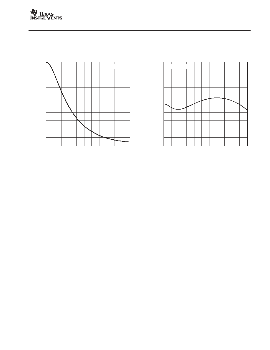
DIGITAL FILTER
Digital Filter Response
Figure 1. Frequency Response, Sharp Rolloff
Frequency [
◊
fS]
-160
-140
-120
-100
-80
-60
-40
-20
0
0
1
2
3
4
Amplitude - dB
AMPLITUDE
vs
FREQUENCY
Figure 2. Pass-Band Ripple, Sharp Rolloff
Frequency [
◊
fS]
-3
-2
-1
0
1
2
3
0.0
0.1
0.2
0.3
0.4
0.5
AMPLITUDE
vs
FREQUENCY
0.003
0
-0.001
-0.003
0.001
0.002
-0.002
Amplitude - dB
Figure 3. Frequency Response, Slow Rolloff
Frequency [
◊
fS]
-140
-120
-100
-80
-60
-40
-20
0
0
1
2
3
4
Amplitude - dB
AMPLITUDE
vs
FREQUENCY
Figure 4. Transition Characteristics, Slow Rolloff
Frequency [
◊
fS]
-20
-18
-16
-14
-12
-10
-8
-6
-4
-2
0
0.0
0.1
0.2
0.3
0.4
0.5
0.6
Amplitude - dB
AMPLITUDE
vs
FREQUENCY
PCM1793
SLES076A - MARCH 2003 - REVISED JANUARY 2004
www.ti.com
8
De-Emphasis Filter
Figure 5
f - Frequency - kHz
-10
-9
-8
-7
-6
-5
-4
-3
-2
-1
0
0
2
4
6
8
10
12
14
De-emphasis Level - dB
DE-EMPHASIS LEVEL
vs
FREQUENCY
fS = 32 kHz
Figure 6
f - Frequency - kHz
-0.5
-0.4
-0.3
-0.2
-0.1
-0.0
0.1
0.2
0.3
0.4
0.5
0
2
4
6
8
10
12
14
DE-EMPHASIS ERROR
vs
FREQUENCY
fS = 32 kHz
De-emphasis Error - dB
0.0
Figure 7
f - Frequency - kHz
-10
-9
-8
-7
-6
-5
-4
-3
-2
-1
0
0
2
4
6
8
10
12
14
16
18
20
De-emphasis Level - dB
DE-EMPHASIS LEVEL
vs
FREQUENCY
fS = 44.1 kHz
Figure 8
f - Frequency - kHz
-0.5
-0.4
-0.3
-0.2
-0.1
-0.0
0.1
0.2
0.3
0.4
0.5
0
2
4
6
8
10
12
14
16
18
20
DE-EMPHASIS ERROR
vs
FREQUENCY
0.0
fS = 44.1 kHz
De-emphasis Error - dB
PCM1793
SLES076A - MARCH 2003 - REVISED JANUARY 2004
www.ti.com
9
De-Emphasis Filter (Continued)
Figure 9
f - Frequency - kHz
-10
-9
-8
-7
-6
-5
-4
-3
-2
-1
0
0
2
4
6
8
10
12
14
16
18
20
22
De-emphasis Level - dB
DE-EMPHASIS LEVEL
vs
FREQUENCY
fS = 48 kHz
Figure 10
f - Frequency - kHz
-0.5
-0.4
-0.3
-0.2
-0.1
-0.0
0.1
0.2
0.3
0.4
0.5
0
2
4
6
8
10
12
14
16
18
20
22
DE-EMPHASIS ERROR
vs
FREQUENCY
fS = 48 kHz
De-emphasis Error - dB
0.0
PCM1793
SLES076A - MARCH 2003 - REVISED JANUARY 2004
www.ti.com
10
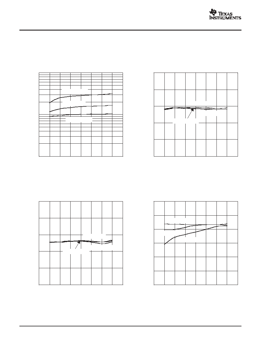
ANALOG DYNAMIC PERFORMANCE
Supply Voltage Characteristics
Figure 11
4.00
4.25
4.50
4.75
5.00
5.25
5.50
5.75
6.00
VCC - Supply Voltage - V
TOTAL HARMONIC DISTORTION + NOISE
vs
SUPPLY VOLTAGE
0.01
0.001
0.0001
fS = 192 kHz
fS = 96 kHz
THD+N - T
otal Harmonic Distortion + Noise - %
fS = 44.1 kHz
Figure 12
VCC - Supply Voltage - V
108
110
112
114
116
118
4.00
4.25
4.50
4.75
5.00
5.25
5.50
5.75
6.00
Dynamic Range - dB
DYNAMIC RANGE
vs
SUPPLY VOLTAGE
fS = 96 kHz
fS = 44.1 kHz
fS = 192 kHz
Figure 13
VCC - Supply Voltage - V
108
110
112
114
116
118
4.00
4.25
4.50
4.75
5.00
5.25
5.50
5.75
6.00
SNR - Signal-to-Noise Ratio - dB
SIGNAL-to-NOISE RATIO
vs
SUPPLY VOLTAGE
fS = 96 kHz
fS = 192 kHz
fS = 44.1 kHz
Figure 14
VCC - Supply Voltage - V
102
104
106
108
110
112
114
4.00
4.25
4.50
4.75
5.00
5.25
5.50
5.75
6.00
Channel Separation - dB
CHANNEL SEPARATION
vs
SUPPLY VOLTAGE
fS = 96 kHz
fS = 192 kHz
fS = 44.1 kHz
NOTE: PCM mode, TA = 25
∞
C, VDD = 3.3 V.
PCM1793
SLES076A - MARCH 2003 - REVISED JANUARY 2004
www.ti.com
11
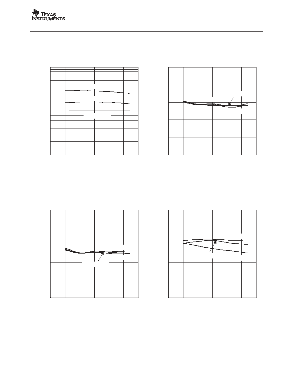
Temperature Characteristics
Figure 15
-50
-25
0
25
50
75
100
TOTAL HARMONIC DISTORTION + NOISE
vs
FREE-AIR TEMPERATURE
0.01
0.001
0.0001
fS = 192 kHz
fS = 96 kHz
THD+N - T
otal Harmonic Distortion + Noise - %
fS = 44.1 kHz
TA - Free-Air Temperature -
∞
C
Figure 16
TA - Free-Air Temperature -
∞
C
108
110
112
114
116
118
-50
-25
0
25
50
75
100
Dynamic Range - dB
DYNAMIC RANGE
vs
FREE-AIR TEMPERATURE
fS = 192 kHz
fS = 44.1 kHz
fS = 96 kHz
Figure 17
TA - Free-Air Temperature -
∞
C
108
110
112
114
116
118
-50
-25
0
25
50
75
100
SNR - Signal-to-Noise Ratio - dB
SIGNAL-to-NOISE RATIO
vs
FREE-AIR TEMPERATURE
fS = 96 kHz
fS = 44.1 kHz
fS = 192 kHz
Figure 18
TA - Free-Air Temperature -
∞
C
104
106
108
110
112
114
-50
-25
0
25
50
75
100
Channel Separation - dB
CHANNEL SEPARATION
vs
FREE-AIR TEMPERATURE
fS = 192 kHz
fS = 44.1 kHz
fS = 96 kHz
NOTE: PCM mode, VDD = 3.3 V, VCC = 5 V.
PCM1793
SLES076A - MARCH 2003 - REVISED JANUARY 2004
www.ti.com
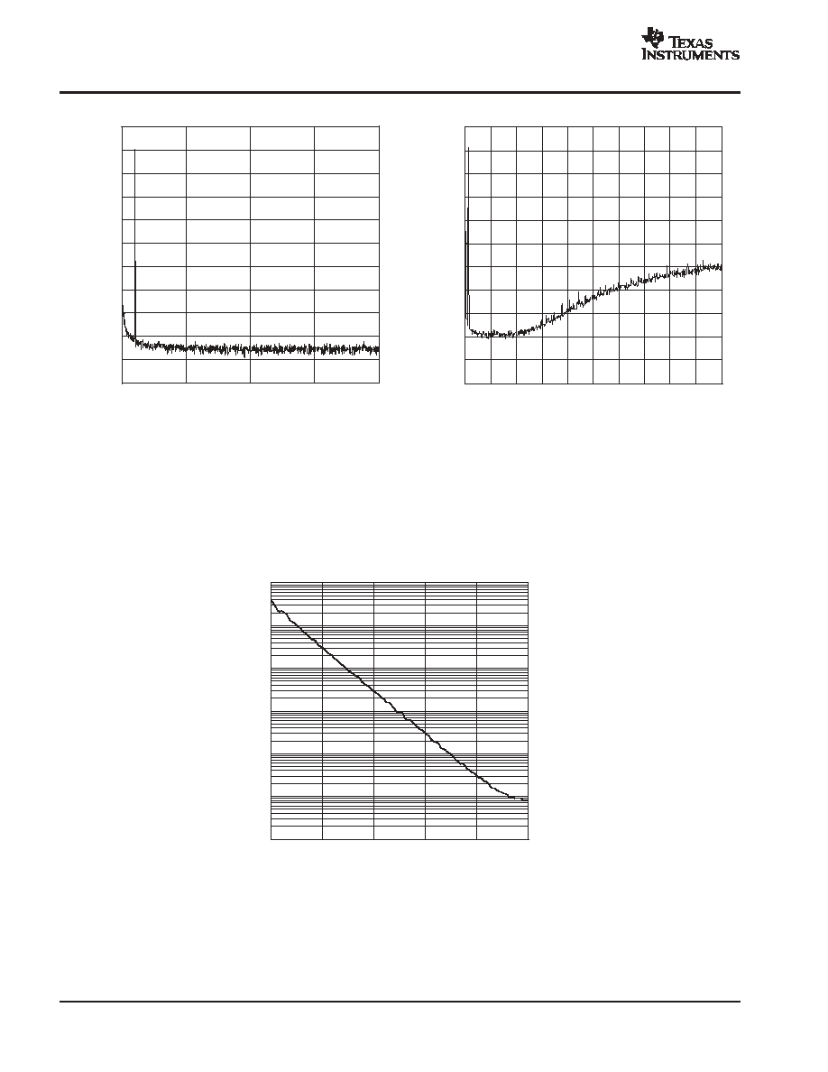
12
f - Frequency - kHz
-160
-150
-140
-130
-120
-110
-100
-90
-80
-70
-60
-50
0
5
10
15
20
Amplitude - dB
AMPLITUDE vs FREQUENCY
Figure 19. -60-dB Output Spectrum, BW = 20 kHz
Figure 20. -60-dB Output Spectrum, BW = 100 kHz
f - Frequency - kHz
-160
-150
-140
-130
-120
-110
-100
-90
-80
-70
-60
-50
0
10
20
30
40
50
60
70
80
90
100
Amplitude - dB
AMPLITUDE vs FREQUENCY
NOTE: PCM mode, fS = 44.1 kHz, 32768 points, 8 average, TA = 25
∞
C, VDD = 3.3 V, VCC = 5 V.
-100
-80
-60
-40
-20
0
Input Level - dBFS
TOTAL HARMONIC DISTORTION + NOISE
vs
INPUT LEVEL
100
0.1
0.01
0.001
0.0001
THD+N - T
otal Harmonic Distortion + Noise - %
1
10
Figure 21. THD+N vs Input Level, PCM Mode
NOTE: PCM mode, fS = 44.1 kHz, TA = 25
∞
C, VDD = 3.3 V, VCC = 5 V.
PCM1793
SLES076A - MARCH 2003 - REVISED JANUARY 2004
www.ti.com
13
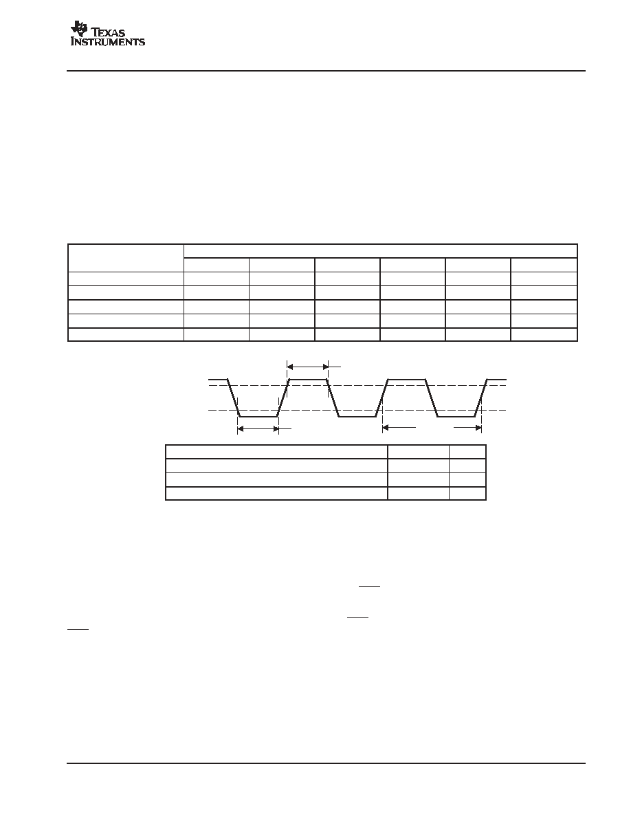
SYSTEM CLOCK AND RESET FUNCTIONS
System Clock Input
The PCM1793 requires a system clock for operating the digital interpolation filters and advanced segment DAC
modulators. The system clock is applied at the SCK input (pin 5). The PCM1793 has a system clock detection circuit
that automatically senses which frequency the system clock is operating. Table 1 shows examples of system clock
frequencies for common audio sampling rates.
Figure 22 shows the timing requirements for the system clock input. For optimal performance, it is important to use
a clock source with low phase jitter and noise. One of the Texas Instruments' PLL1700 family of multiclock generators
is an excellent choice for providing the PCM1793 system clock.
Table 1. System Clock Rates for Common Audio Sampling Frequencies
SAMPLING FREQUENCY
SYSTEM CLOCK FREQUENCY (FSCK) (MHZ)
SAMPLING FREQUENCY
128 fS
192 fS
256 fS
384 fS
512 fS
768 fS
32 kHz
4.096
6.144
8.192
12.288
16.384
24.576
44.1 kHz
5.6488
8.4672
11.2896
16.9344
22.5792
33.8688
48 kHz
6.144
9.216
12.288
18.432
24.576
36.864
96 kHz
12.288
18.432
24.576
36.864
49.152
73.728
192 kHz
24.576
36.864
49.152
73.728
(1)
(1)
(1) This system clock rate is not supported for the given sampling frequency.
t(SCKH)
System Clock (SCK)
t(SCKL)
2.0 V
0.8 V
H
L
t(SCY)
PARAMETERS
MIN
MAX
UNITS
t(SCY)
System clock pulse cycle time
13
ns
t(SCKH) System clock pulse duration, HIGH
5
ns
t(SCKL) System clock pulse duration, LOW
5
ns
Figure 22. System Clock Input Timing
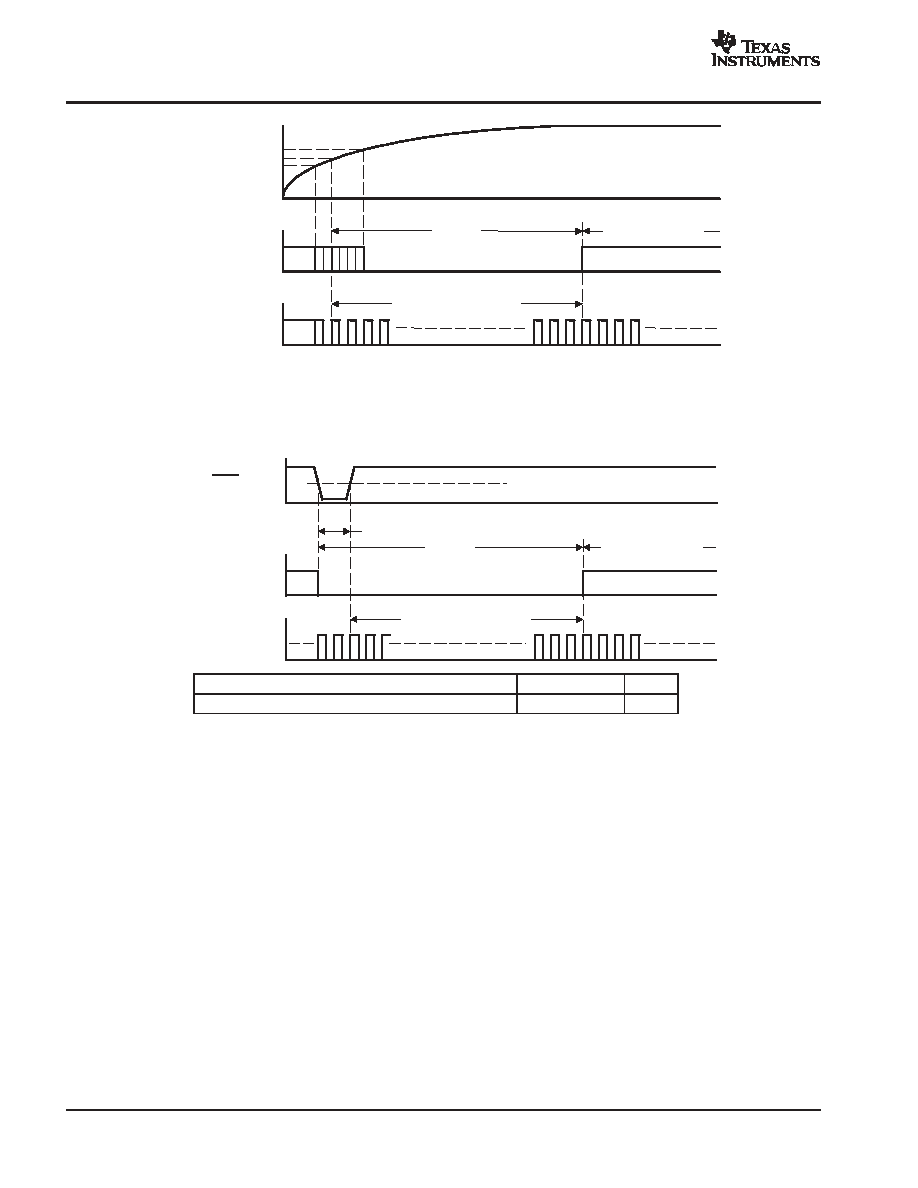
Power-On and External Reset Functions
The PCM1793 includes a power-on reset function. Figure 23 shows the operation of this function. With V
DD
> 2 V,
the power-on reset function is enabled. The initialization sequence requires 1024 system clocks from the time
V
DD
> 2 V.
The PCM1793 also includes an external reset capability using the RST input (pin 6). This allows an external controller
or master reset circuit to force the PCM1793 to initialize to its default reset state.
Figure 24 shows the external reset operation and timing. The RST pin is set to logic 0 for a minimum of 20 ns. The
RST pin is then set to a logic 1 state, thus starting the initialization sequence, which requires 1024 system clock
periods. The external reset is especially useful in applications where there is a delay between the PCM1793 power
up and system clock activation.
PCM1793
SLES076A - MARCH 2003 - REVISED JANUARY 2004
www.ti.com
14
Reset
Reset Removal
1024 System Clocks
VDD
2.4 V (Max)
2.0 V (Typ)
1.6 V (Min)
Internal Reset
System Clock
Figure 23. Power-On Reset Timing
Reset
Reset Removal
1024 System Clocks
Internal Reset
System Clock
RST (Pin 6)
t(RST)
1.4 V
PARAMETERS
MIN
MAX
UNITS
t(RST)
Reset pulse duration, LOW
20
ns
Figure 24. External Reset Timing
PCM1793
SLES076A - MARCH 2003 - REVISED JANUARY 2004
www.ti.com
15
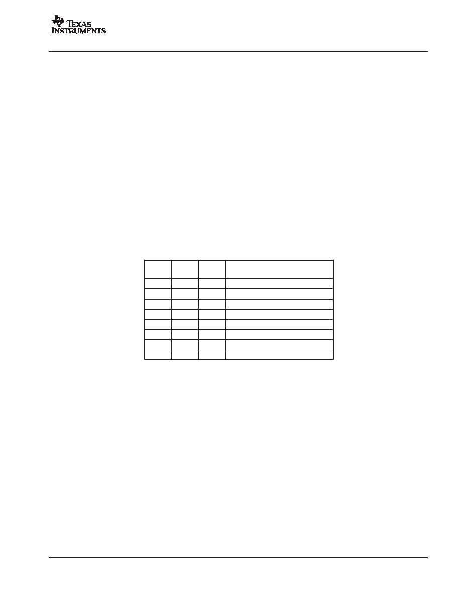
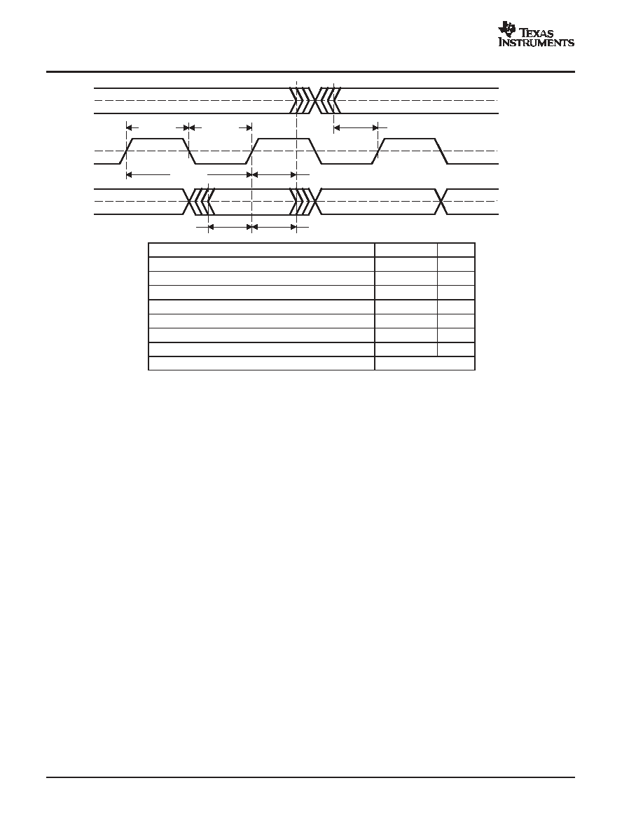
AUDIO DATA INTERFACE
Audio Serial Interface
The audio interface port is a 3-wire serial port. It includes LRCK (pin 1), BCK (pin 2), and DATA (pin 3). BCK is the
serial audio bit clock, and it is used to clock the serial data present on DATA into the serial shift register of the audio
interface. Serial data is clocked into the PCM1793 on the rising edge of BCK. LRCK is the serial audio left/right word
clock.
The PCM1793 requires the synchronization of LRCK and the system clock, but does not need a specific phase
relation between LRCK and the system clock.
If the relationship between LRCK and the system clock changes more than
±
6 BCK, internal operation is initialized
within 1/f
S
and the analog outputs are forced to the bipolar zero level until resynchronization between LRCK and the
system clock is completed.
PCM Audio Data Formats and Timing
The PCM1793 supports industry-standard audio data formats, including standard right-justified, I
2
S, and
left-justified. The data formats are shown in Figure 26. Data formats are selected using the format bits,
FMT2 (pin 28), FMT1 (pin27), and FMT0 (pin26) as shown in Table 2. All formats require binary 2s complement,
MSB-first audio data. Figure 25 shows a detailed timing diagram for the serial audio interface.
Table 2. Audio Data Format Selection
FMT2
PIN 28
FMT1
PIN 27
FMT0
PIN 26
FORMAT
LOW
LOW
LOW
16-bit standard format, right-justified
LOW
LOW
HIGH
20-bit standard format, right-justified
LOW
HIGH
LOW
24-bit standard format, right-justified
LOW
HIGH
HIGH
24-bit MSB-first, left-justified format
HIGH
LOW
LOW
16-bit I2S format
HIGH
LOW
HIGH
24-bit I2S format
HIGH
HIGH
LOW
Reserved
HIGH
HIGH
HIGH
Reserved
PCM1793
SLES076A - MARCH 2003 - REVISED JANUARY 2004
www.ti.com
16
DATA
t(BCH)
1.4 V
BCK
LRCK
t(BCL)
t(LB)
t(BCY)
t(DS)
t(DH)
1.4 V
1.4 V
t(BL)
PARAMETERS
MIN
MAX
UNITS
t(BCY)
BCK pulse cycle time
70
ns
t(BCL)
BCK pulse duration, LOW
30
ns
t(BCH)
BCK pulse duration, HIGH
30
ns
t(BL)
BCK rising edge to LRCK edge
10
ns
t(LB)
LRCK edge to BCK rising edge
10
ns
t(DS)
DATA setup time
10
ns
t(DH)
DATA hold time
10
ns
--
LRCK clock duty
50%
±
2 bit clocks
Figure 25. Timing of Audio Interface
PCM1793
SLES076A - MARCH 2003 - REVISED JANUARY 2004
www.ti.com
17
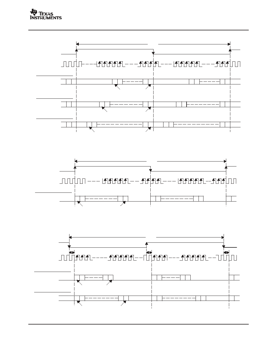
14 15 16
1
2
15 16
MSB
LSB
1
2
15 16
18 19 20
MSB
LSB
1
2
19 20
1
2
19 20
22 23 24
LSB
1
23
2
24
1
23
2
24
2
1
MSB
LSB
1
2
24
1
2
24
LSB
1
2
24
2
1
1
2
24
2
1
LSB
1
2
16
1
2
16
BCK
L-Channel
DATA
R-Channel
1/fS
DATA
DATA
LRCK
Audio Data Word = 16-Bit
Audio Data Word = 20-Bit
Audio Data Word = 24-Bit
BCK
L-Channel
DATA
R-Channel
1/fS
LRCK
Audio Data Word = 24-Bit
23
23
15
15
23
23
BCK
L-Channel
DATA
R-Channel
1/fS
LRCK
Audio Data Word = 24-Bit
DATA
Audio Data Word = 16-Bit
MSB
MSB
MSB
(2) Left Justified Data Format; L-Channel = HIGH, R-Channel = LOW
(1) Standard Data Format (Right Justified); L-Channel = HIGH, R-Channel = LOW
(3) I
2
S Data Format; L-Channel = LOW, R-Channel = HIGH
Figure 26. Audio Data Input Formats
PCM1793
SLES076A - MARCH 2003 - REVISED JANUARY 2004
www.ti.com
18
FUNCTION DESCRIPTIONS
Zero Detect
When the PCM1793 detects that the audio input data in the L-channel or R-channel is continuously zero for 1024
f
S
, the PCM1793 sets ZEROL (pin 23) or ZEROR (pin 22) to HIGH.
Soft Mute
The PCM1793 supports mute operation. When MUTE (pin 4) is set to HIGH, both analog outputs are transitioned
to the bipolar zero level in -0.5-dB steps with a transition speed of 1/f
S
per step. This system provides pop-free muting
of the DAC output.
De-Emphasis
The PCM1793 has de-emphasis filters for sampling frequencies of 32 kHz, 44.1 kHz, and 48 kHz. DEMP1 (pin 25)
and DEMP0 (pin 24) select the sampling frequency for which de-emphasis filtering is performed, as shown in Table 3.
Table 3. De-Emphasis Control
DEMP1
PIN 25
DEMP0
PIN 24
DE-EMPHASIS FUNCTION
LOW
LOW
Disabled
LOW
HIGH
48 kHz
HIGH
LOW
44.1 kHz
HIGH
HIGH
32 kHz
PCM1793
SLES076A - MARCH 2003 - REVISED JANUARY 2004
www.ti.com
19
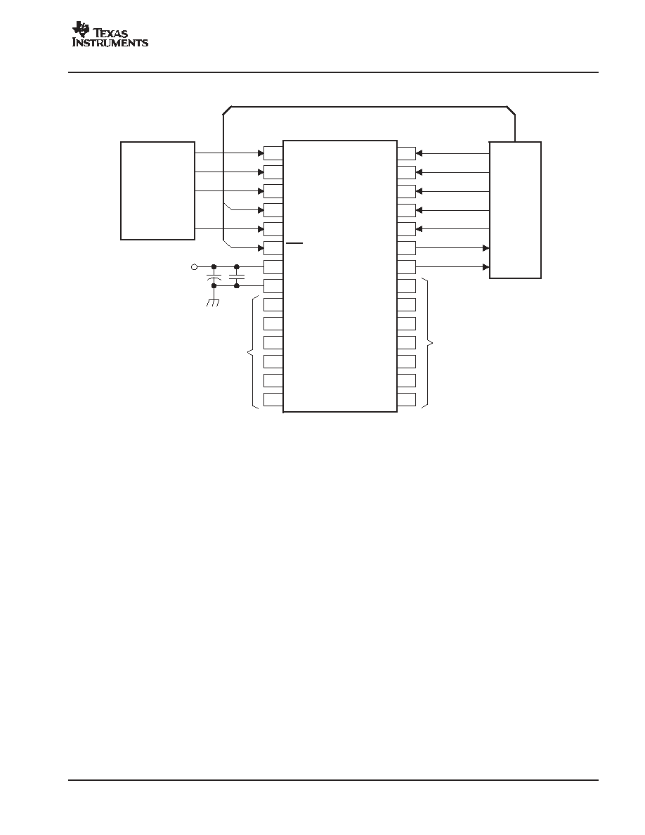
TYPICAL CONNECTION DIAGRAM
SCK
24
23
22
21
20
19
18
17
16
15
5
6
7
8
9
10
11
12
13
14
PCM1793
RST
VDD
DGND
AGNDF
VCCR
AGNDR
VOUTR-
VOUTR+
VCOM
DEMP0
VOUTL-
ZEROL
ZEROR
VCCF
VCCL
VOUTL+
AGNDC
AGNDL
LRCK
1
2
3
4
BCK
DATA
MUTE
28
27
26
25
FMT2
FMT1
FMT0
DEMP1
VCCC
Controller
L/R Clock (fS)
Bit Clock
Audio Data
System Clock
+
3.3 V
Analog
Output Stage
(See Figure 28)
Analog
Output Stage
(See Figure 28)
Figure 27. Typical Application Circuit
PCM1793
SLES076A - MARCH 2003 - REVISED JANUARY 2004
www.ti.com
20
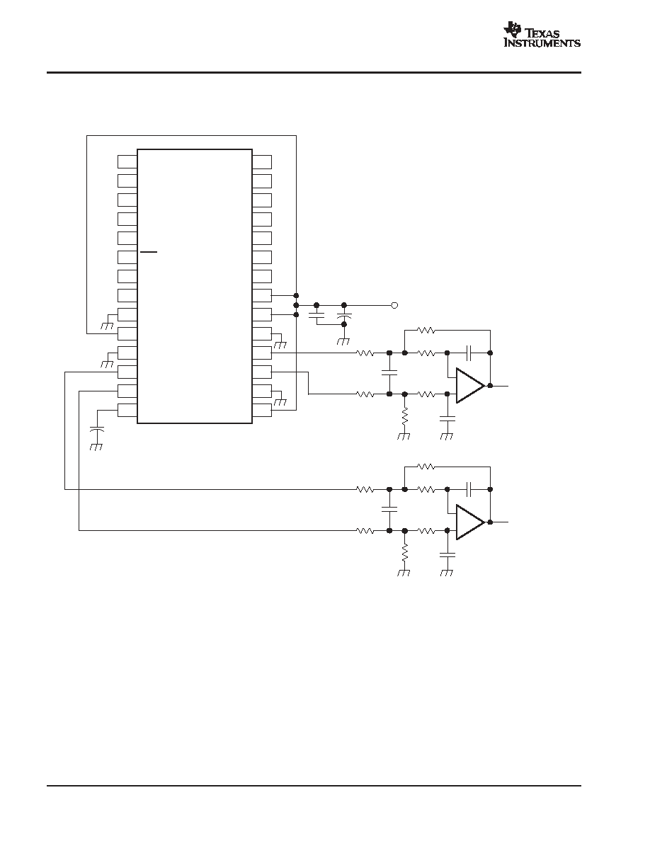
APPLICATION INFORMATION
ANALOG OUTPUTS
SCK
24
23
22
21
20
19
18
17
16
15
5
6
7
8
9
10
11
12
13
14
PCM1793
RST
VDD
DGND
AGNDF
VCCR
AGNDR
VOUTR-
VOUTR+
VCOM
DEMP0
VOUTL-
ZEROL
ZEROR
VCCF
VCCL
VOUTL+
AGNDC
AGNDL
LRCK
1
2
3
4
BCK
DATA
MUTE
28
27
26
25
FMT2
FMT1
FMT0
DEMP1
VCCC
+
1
µ
F
-
+
C3L
R6L
R4L
R5L
C1L
C2L
R3L
R2L
R1L
VOUT
L-Channel
+
5 V
-
+
VOUT
R-Channel
10
µ
F
0.1
µ
F
C3R
R6R
R4R
R5R
C1R
C2R
R3R
R2R
R1R
NOTE: Example R and C values for fC = 77 kHz ≠ R1, R2: 1.8 k
, R3,R4: 3.3 k
, R5,R6: 680
, C1: 1800 pF, C2, C3: 560 pF.
Figure 28. Typical Application for Analog Output Stage
Analog Output Level and LPF
The signal level of the DAC differential-voltage output {(V
OUT
L+)≠(V
OUT
L≠), (V
OUT
R+)≠(V
OUT
R≠)} is 3.2 Vp-p
at 0 dB (full scale). The voltage output of the LPF is given by following equation:
V
OUT
= 3.2 Vp-p
◊
(R
f
/R
i
)
Here, R
f
is the feedback resistor in the LPF, and R
3
= R
4
in a typical application circuit. R
i
is the input resistor
in the LPF, and R
1
= R
2
in a typical application circuit.
Op Amp for LPF
An OPA2134 or 5532 type op amp is recommended for the LPF circuit to obtain the specified audio
performance. Dynamic performance such as gain bandwidth, settling time, and slew rate of the op amp largely
determines the audio dynamic performance of the LPF section. The input noise specification of the op amp
should be considered to obtain a 113-dB S/N ratio.
PCM1793
SLES076A - MARCH 2003 - REVISED JANUARY 2004
www.ti.com
21
Analog Gain of Balanced Amplifier
The DAC voltage outputs are followed by balanced amplifier stages, which sum the differential signals for each
channel, creating a single-ended voltage output. In addition, the balanced amplifiers provide a third-order
low-pass filter function, which band limits the audio output signal. The cutoff frequency and gain are determined
by external R and C component values. In this case, the cutoff frequency is 77 kHz with a gain of 1.83. The
output voltage for each channel is 5.9 Vp-p, or 2.1 V rms.
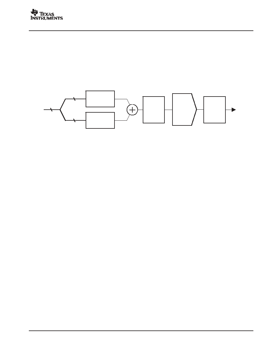
THEORY OF OPERATION
Analog
Voltage
Output
Digital
Input
24 Bit
8 fS
MSB
and
Lower 18 Bit
Upper
6 Bit
ICOB
Decoder
3rd-Order
5-Level
Sigma-Delta
Advanced
DWA
Current
Segment
DAC
0-4
Level
0-62
Level
0-66
I/V
Converter
Figure 29. Advanced Segment DAC With I/V Converter
The PCM1793 uses TI's advanced segment DAC architecture to achieve excellent dynamic performance and
improved tolerance to clock jitter. The PCM1793 provides balanced voltage outputs.
Digital input data via the digital filter is separated into 6 upper bits and 18 lower bits. The 6 upper bits are converted
to inverted complementary offset binary (ICOB) code. The lower 18 bits, associated with the MSB, are processed
by a five-level third-order delta-sigma modulator operated at 64 f
S
by default. The 1 level of the modulator is equivalent
to the 1 LSB of the ICOB code converter. The data groups processed in the ICOB converter and third-order
delta-sigma modulator are summed together to an up-to-66-level digital code, and then processed by data-weighted
averaging (DWA) to reduce the noise produced by element mismatch. The data of up to 66 levels from the DWA is
converted to an analog output in the differential-current segment section.
This architecture has overcome the various drawbacks of conventional multibit processing and also achieves
excellent dynamic performance.
PCM1793
SLES076A - MARCH 2003 - REVISED JANUARY 2004
www.ti.com
22
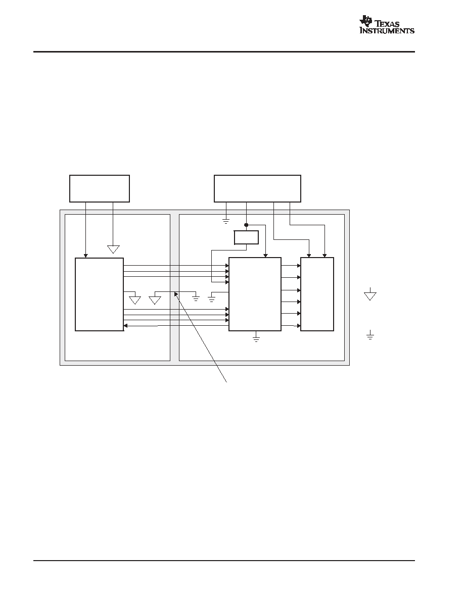
CONSIDERATIONS FOR APPLICATION CIRCUITS
PCB Layout Guidelines
A typical PCB floor plan for the PCM1793 is shown in Figure 30. A ground plane is recommended, with the analog
and digital sections being isolated from one another using a split or cut in the circuit board. The PCM1793 must be
oriented with the digital I/O pins facing the ground plane split/cut to allow for short, direct connections to the digital
audio interface and control signals originating from the digital section of the board. Separate power supplies are
recommended for the digital and analog sections of the board. This prevents the switching noise present on the digital
supply from contaminating the analog power supply and degrading the dynamic performance of the D/A converters.
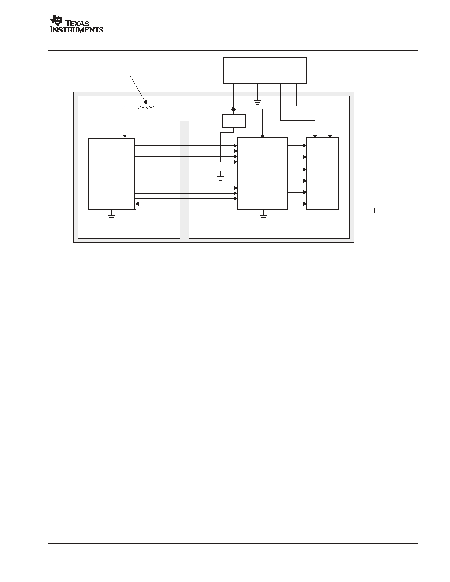
In cases where a common 5-V supply would be used for the analog and digital sections, an inductance (RF choke,
ferrite bead) must be placed between the analog and digital 5-V supply connections to avoid coupling of the digital
switching noise into the analog circuitry. Figure 31 shows the recommended approach for single-supply applications.
Digital Logic
and
Audio
Processor
Digital Power
+VD
DGND
Digital Section
Analog Section
Return Path for Digital Signals
Analog Power
+VS
AGND
-VS
+5VA
Digital
Ground
Analog
Ground
Output
Circuits
PCM1793
AGND
VCC
VDD
DGND
REG
Figure 30. Recommended PCB Layout
PCM1793
SLES076A - MARCH 2003 - REVISED JANUARY 2004
www.ti.com
23
VDD
Digital Section
Analog Section
RF Choke or Ferrite Bead
Power Supplies
Common
Ground
Output
Circuits
AGND
VCC
+VS
+5V
-VS
AGND
VDD
DGND
REG
PCM1793
Figure 31. Single-Supply PCB Layout
Bypass and Decoupling Capacitor Requirements
Various-sized decoupling capacitors can be used, with no special tolerances being required. All capacitors must be
located as close as possible to the appropriate pins of the PCM1793 to reduce noise pickup from surrounding circuitry.
Aluminum electrolytic capacitors that are designed for hi-fi audio applications are recommended for larger values,
while metal film or monolithic ceramic capacitors are used for smaller values.
Post-LPF Design
By proper choice of the op amp and resistors used in the post-LPF circuit, excellent performance of the PCM1793
should be achieved. To obtain 0.001% THD+N, 113 dB signal-to-noise-ratio audio performance, the THD+N and input
noise performance of the op amp must be considered. This is because the input noise of the op amp contributes
directly to the output noise level of the application. The V
OUT
pins of the PCM1793 and the input resistor of the
post-LPF circuit must be connected as closely as possible.
Out-of-band noise level and attenuated sampling spectrum level are much lower than for typical delta-sigma type
DACs due to the combination of a high-performance digital filter and advanced segment DAC architecture. The use
of a second-order or third-order post-LPF is recommended for the post-LPF of the PCM1793. The cutoff frequency
of the post-LPF depends on the application. For example, there are many sampling-rate operations such as
f
S
= 44.1 kHz on CDDA, f
S
= 96 kHz on DVD-M, f
S
= 192 kHz on DVD-A, f
S
= 64 f
S
on DSD (SACD).
PCM1793
SLES076A - MARCH 2003 - REVISED JANUARY 2004
www.ti.com
24
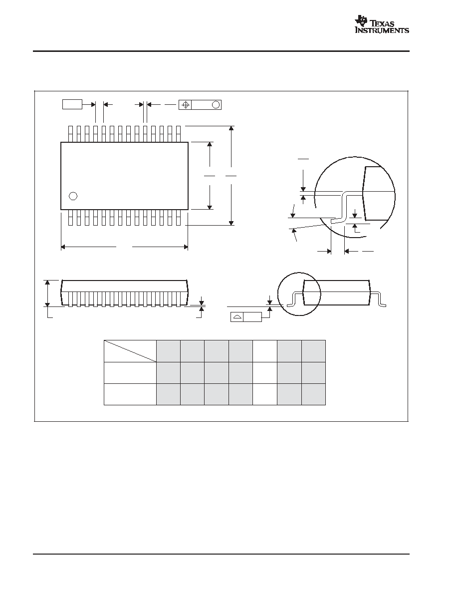
MECHANICAL DATA
DB (R-PDSO-G**)
PLASTIC SMALL-OUTLINE
4040065 /E 12/01
28 PINS SHOWN
Gage Plane
8,20
7,40
0,55
0,95
0,25
38
12,90
12,30
28
10,50
24
8,50
Seating Plane
9,90
7,90
30
10,50
9,90
0,38
5,60
5,00
15
0,22
14
A
28
1
20
16
6,50
6,50
14
0,05 MIN
5,90
5,90
DIM
A MAX
A MIN
PINS **
2,00 MAX
6,90
7,50
0,65
M
0,15
0
∞
-8
∞
0,10
0,09
0,25
NOTES: A. All linear dimensions are in millimeters.
B. This drawing is subject to change without notice.
C. Body dimensions do not include mold flash or protrusion not to exceed 0,15.
D. Falls within JEDEC MO-150

IMPORTANT NOTICE
Texas Instruments Incorporated and its subsidiaries (TI) reserve the right to make corrections, modifications,
enhancements, improvements, and other changes to its products and services at any time and to discontinue
any product or service without notice. Customers should obtain the latest relevant information before placing
orders and should verify that such information is current and complete. All products are sold subject to TI's terms
and conditions of sale supplied at the time of order acknowledgment.
TI warrants performance of its hardware products to the specifications applicable at the time of sale in
accordance with TI's standard warranty. Testing and other quality control techniques are used to the extent TI
deems necessary to support this warranty. Except where mandated by government requirements, testing of all
parameters of each product is not necessarily performed.
TI assumes no liability for applications assistance or customer product design. Customers are responsible for
their products and applications using TI components. To minimize the risks associated with customer products
and applications, customers should provide adequate design and operating safeguards.
TI does not warrant or represent that any license, either express or implied, is granted under any TI patent right,
copyright, mask work right, or other TI intellectual property right relating to any combination, machine, or process
in which TI products or services are used. Information published by TI regarding third-party products or services
does not constitute a license from TI to use such products or services or a warranty or endorsement thereof.
Use of such information may require a license from a third party under the patents or other intellectual property
of the third party, or a license from TI under the patents or other intellectual property of TI.
Reproduction of information in TI data books or data sheets is permissible only if reproduction is without
alteration and is accompanied by all associated warranties, conditions, limitations, and notices. Reproduction
of this information with alteration is an unfair and deceptive business practice. TI is not responsible or liable for
such altered documentation.
Resale of TI products or services with statements different from or beyond the parameters stated by TI for that
product or service voids all express and any implied warranties for the associated TI product or service and
is an unfair and deceptive business practice. TI is not responsible or liable for any such statements.
Following are URLs where you can obtain information on other Texas Instruments products and application
solutions:
Products
Applications
Amplifiers
amplifier.ti.com
Audio
www.ti.com/audio
Data Converters
dataconverter.ti.com
Automotive
www.ti.com/automotive
DSP
dsp.ti.com
Broadband
www.ti.com/broadband
Interface
interface.ti.com
Digital Control
www.ti.com/digitalcontrol
Logic
logic.ti.com
Military
www.ti.com/military
Power Mgmt
power.ti.com
Optical Networking
www.ti.com/opticalnetwork
Microcontrollers
microcontroller.ti.com
Security
www.ti.com/security
Telephony
www.ti.com/telephony
Video & Imaging
www.ti.com/video
Wireless
www.ti.com/wireless
Mailing Address:
Texas Instruments
Post Office Box 655303 Dallas, Texas 75265
Copyright
2004, Texas Instruments Incorporated