 | –≠–ª–µ–∫—Ç—Ä–æ–Ω–Ω—ã–π –∫–æ–º–ø–æ–Ω–µ–Ω—Ç: PCM1798 | –°–∫–∞—á–∞—Ç—å:  PDF PDF  ZIP ZIP |
PCM1798
SLES102 ≠ DECEMBER 2003
24 BIT, 192 kHz SAMPLING, ADVANCED SEGMENT,
AUDIO STEREO DIGITAL TO ANALOG CONVERTER
FEATURES
D
24-Bit Resolution
D
Analog Performance:
- Dynamic Range: 123 dB
- THD+N: 0.0005%
D
Differential Current Output: 4 mA p-p
D
8◊ Oversampling Digital Filter:
- Stop-Band Attenuation: ≠98 dB
- Pass-Band Ripple: ±0.0002 dB
D
Sampling Frequency: 10 kHz to 200 kHz
D
System Clock: 128, 192, 256, 384, 512, or
768 f
S
With Autodetect
D
Accepts 16- and 24-Bit Audio Data
D
PCM Data Formats: Standard, I
2
S, and
Left-Justified
D
Interface Available for Optional External
Digital Filter or DSP
D
Digital De-Emphasis
D
Digital Filter Rolloff: Sharp or Slow
D
Soft Mute
D
Zero Flag
D
Dual-Supply Operation: 5-V Analog, 3.3-V
Digital
D
5-V Tolerant Digital Inputs
D
Small 28-Lead SSOP Package, Lead-Free
Product
D
Pin Assignment Compatible With PCM1794
APPLICATIONS
D
A/V Receivers
D
DVD Players
D
Musical Instruments
D
HDTV Receivers
D
Car Audio Systems
D
Digital Multitrack Recorders
D
Other Applications Requiring 24-Bit Audio
DESCRIPTION
The PCM1798 is a monolithic CMOS integrated circuit that
includes stereo digital-to-analog converters and support
circuitry in a small 28-lead SSOP package. The data
converters use TI's advanced segment DAC architecture
to achieve excellent dynamic performance and improved
tolerance to clock jitter. The PCM1798 provides balanced
current outputs, allowing the user to optimize analog
performance externally. Sampling rates up to 200 kHz are
supported.
This integrated circuit can be damaged by ESD. Texas Instruments recommends that all integrated circuits be handled with appropriate
precautions. Failure to observe proper handling and installation procedures can cause damage.
ESD damage can range from subtle performance degradation to complete device failure. Precision integrated circuits may be more susceptible to
damage because very small parametric changes could cause the device not to meet its published specifications.
Please be aware that an important notice concerning availability, standard warranty, and use in critical applications of Texas Instruments
semiconductor products and disclaimers thereto appears at the end of this data sheet.
Burr Brown Products
from Texas Instruments
Copyright
2003, Texas Instruments Incorporated
PRODUCTION DATA information is current as of publication date. Products
conform to specifications per the terms of Texas Instruments standard warranty.
Production processing does not necessarily include testing of all parameters.
PCM1798
SLES102 ≠ DECEMBER 2003
www.ti.com
2
ORDERING INFORMATION
PRODUCT
PACKAGE
PACKAGE CODE
OPERATION
TEMPERATURE
RANGE
PACKAGE
MARKING
ORDERING
NUMBER
TRANSPORT
MEDIA
PCM1798DB
28 lead SSOP
28DB
25
∞
C to 85
∞
C
PCM1798
PCM1798DB
Tube
PCM1798DB
28-lead SSOP
28DB
≠25
∞
C to 85
∞
C
PCM1798
PCM1798DBR
Tape and reel
ABSOLUTE MAXIMUM RATINGS
over operating free-air temperature range unless otherwise noted(1)
PCM1798
Supply voltage
VCC1, VCC2L, VCC2R
≠0.3 V to 6.5 V
Supply voltage
VDD
≠0.3 V to 4 V
Supply voltage differences: VCC1, VCC2L, VCC2R
±
0.1 V
Ground voltage differences: AGND1, AGND2, AGND3L, AGND3R, DGND
±
0.1 V
Digital input voltage
LRCK, DATA, BCK, SCK, FMT1, FMT0, MONO, CHSL, DEM, MUTE, RST,
≠0.3 V to 6.5 V
Digital input voltage
ZERO
≠0.3 V to (VDD + 0.3 V) < 4 V
Analog input voltage
≠0.3 V to (VCC + 0.3 V) < 6.5 V
Input current (any pins except supplies)
±
10 mA
Ambient temperature under bias
≠40
∞
C to 125
∞
C
Storage temperature
≠55
∞
C to 150
∞
C
Junction temperature
150
∞
C
Lead temperature (soldering)
260
∞
C, 5 s
Package temperature (IR reflow, peak)
260
∞
C
(1) Stresses beyond those listed under "absolute maximum ratings" may cause permanent damage to the device. These are stress ratings only, and
functional operation of the device at these or any other conditions beyond those indicated under "recommended operating conditions" is not
implied. Exposure to absolute-maximum-rated conditions for extended periods may affect device reliability.
ELECTRICAL CHARACTERISTICS
all specifications at TA = 25
∞
C, VCC1 = VCC2L = VCC2R = 5 V, VDD = 3.3 V, fS = 44.1 kHz, system clock = 256 fS, and 24-bit data, unless
otherwise noted
PARAMETER
TEST CONDITIONS
PCM1798DB
UNIT
PARAMETER
TEST CONDITIONS
MIN
TYP
MAX
UNIT
RESOLUTION
24
Bits
DATA FORMAT
Audio data interface format
Standard, I2S, left-justified
Audio data bit length
16-, 24-bit selectable
Audio data format
MSB first, 2s complement
fS
Sampling frequency
10
200
kHz
System clock frequency
128, 192, 256, 384, 512, 768 fS
DIGITAL INPUT/OUTPUT
Logic family
TTL compatible
VIH
Input logic level
2
VDC
VIL
Input logic level
0.8
VDC
IIH
Input logic current
VIN = VDD
10
µ
A
IIL
Input logic current
VIN = 0 V
≠10
µ
A
VOH
O t t l i l
l
IOH = ≠2 mA
2.4
VDC
VOL
Output logic level
IOL = 2 mA
0.4
VDC

PCM1798
SLES102 ≠ DECEMBER 2003
www.ti.com
3
ELECTRICAL CHARACTERISTICS (Continued)
all specifications at TA = 25
∞
C, VCC1 = VCC2L = VCC2R = 5 V, VDD = 3.3 V, fS = 44.1 kHz, system clock = 256 fS, and 24-bit data, unless
otherwise noted
PARAMETER
TEST CONDITIONS
PCM1798DB
UNIT
PARAMETER
TEST CONDITIONS
MIN
TYP
MAX
UNIT
DYNAMIC PERFORMANCE (1)(2)
fS = 44.1 kHz
0.0005%
0.001%
THD+N at VOUT = 0 dB
fS = 96 kHz
0.001%
THD+N at VOUT 0 dB
fS = 192 kHz
0.0015%
EIAJ, A-weighted, fS = 44.1 kHz
120
123
Dynamic range
EIAJ, A-weighted, fS = 96 kHz
123
dB
Dynamic range
EIAJ, A-weighted, fS = 192 kHz
123
dB
EIAJ, A-weighted, fS = 44.1 kHz
120
123
Signal-to-noise ratio
EIAJ, A-weighted, fS = 96 kHz
123
dB
Signal to noise ratio
EIAJ, A-weighted, fS = 192 kHz
123
dB
fS = 44.1 kHz
116
119
Channel separation
fS = 96 kHz
118
dB
Channel separation
fS = 192 kHz
117
dB
Level linearity error
VOUT = ≠120 dB
±
1
dB
DYNAMIC PERFORMANCE (MONO MODE) (1)(2)(3)
fS = 44.1 kHz
0.0005%
THD+N at VOUT = 0 dB
fS = 96 kHz
0.001%
THD+N at VOUT 0 dB
fS = 192 kHz
0.0015%
EIAJ, A-weighted, fS = 44.1 kHz
126
Dynamic range
EIAJ, A-weighted, fS = 96 kHz
126
dB
Dynamic range
EIAJ, A-weighted, fS = 192 kHz
126
dB
EIAJ, A-weighted, fS = 44.1 kHz
126
Signal-to-noise ratio
EIAJ, A-weighted, fS = 96 kHz
126
dB
Signal to noise ratio
EIAJ, A-weighted, fS = 192 kHz
126
dB
(1) Filter condition:
THD+N: 20-Hz HPF, 20-kHz AES17 LPF
Dynamic range: 20-Hz HPF, 20-kHz AES17 LPF, A-weighted
Signal-to-noise ratio: 20-Hz HPF, 20-kHz AES17 LPF, A-weighted
Channel separation: 20-Hz HPF, 20-kHz AES17 LPF
Analog performance specifications are measured using the System Two
t
Cascade audio measurement system by Audio Precision
in the
averaging mode.
(2) Dynamic performance and dc accuracy are specified at the output of the postamplifier as shown in Figure 24.
(3) Dynamic performance and dc accuracy are specified at the output of the measurement circuit as shown in Figure 25.
Audio Precision and System Two are trademarks of Audio Precision, Inc.
Other trademarks are the property of their respective owners.
PCM1798
SLES102 ≠ DECEMBER 2003
www.ti.com
4
ELECTRICAL CHARACTERISTICS (Continued)
all specifications at TA = 25
∞
C, VCC1 = VCC2L = VCC2R = 5 V, VDD = 3.3 V, fS = 44.1 kHz, system clock = 256 fS, and 24-bit data, unless
otherwise noted
PARAMETER
TEST CONDITIONS
PCM1798DB
UNIT
PARAMETER
TEST CONDITIONS
MIN
TYP
MAX
UNIT
ANALOG OUTPUT
Gain error
≠7
±
2
7
% of FSR
Gain mismatch, channel-to-channel
≠3
±
0.5
3
% of FSR
Bipolar zero error
At BPZ
≠2
±
0.5
2
% of FSR
Output current
Full scale (0 dB)
4
mA p-p
Center current
At BPZ
≠3.5
mA
DIGITAL FILTER PERFORMANCE
De-emphasis error
±
0.1
dB
FILTER CHARACTERISTICS≠1: SHARP ROLLOFF
Pass band
±
0.0002 dB
0.454 fS
Pass band
≠3 dB
0.49 fS
Stop band
0.546 fS
Pass-band ripple
±
0.0002
dB
Stop-band attenuation
Stop band = 0.546 fS
≠98
dB
Delay time
38/fS
s
FILTER CHARACTERISTICS≠2: SLOW ROLLOFF
Pass band
±
0.001 dB
0.21 fS
Pass band
≠3 dB
0.448 fS
Stop band
0.79 fS
Pass-band ripple
±
0.001
dB
Stop-band attenuation
Stop band = 0.732 fS
≠80
dB
Delay time
38/fS
s
POWER SUPPLY REQUIREMENTS
VDD
3
3.3
3.6
VDC
VCC1
Voltage range
VCC2L
Voltage range
4.75
5
5.25
VDC
VCC2R
4.75
5
5.25
VDC
fS = 44.1 kHz
7
9
IDD
fS = 96 kHz
13
mA
IDD
Supply current (1)
fS = 192 kHz
25
mA
Supply current (1)
fS = 44.1 kHz
18
23
ICC
fS = 96 kHz
19
mA
ICC
fS = 192 kHz
20
mA
fS = 44.1 kHz
115
150
Power dissipation (1)
fS = 96 kHz
140
mW
Power dissipation ( )
fS = 192 kHz
180
mW
TEMPERATURE RANGE
Operation temperature
≠25
85
∞
C
JA
Thermal resistance
28-pin SSOP
100
∞
C/W
(1) Input is BPZ data.
PCM1798
SLES102 ≠ DECEMBER 2003
www.ti.com
5
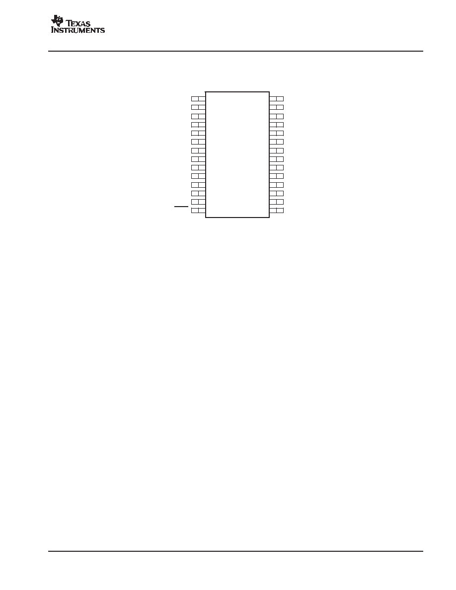
PIN ASSIGNMENTS
1
2
3
4
5
6
7
8
9
10
11
12
13
14
28
27
26
25
24
23
22
21
20
19
18
17
16
15
MONO
CHSL
DEM
LRCK
DATA
BCK
SCK
DGND
V
DD
MUTE
FMT0
FMT1
ZERO
RST
V
CC
2L
AGND3L
I
OUT
L≠
I
OUT
L+
AGND2
V
CC
1
V
COM
L
V
COM
R
I
REF
AGND1
I
OUT
R≠
I
OUT
R+
AGND3R
V
CC
2R
PCM1798
(TOP VIEW)