49%
FPO
PCM1801
FEATURES
q
DUAL 16-BIT MONOLITHIC
ADC
q
SINGLE-ENDED VOLTAGE INPUT
q
64X OVERSAMPLING DECIMATION FILTER:
Passband Ripple:
±
0.05dB
Stopband Attenuation: ≠65dB
q
ANALOG PERFORMANCE:
THD+N: ≠88dB (typ)
SNR: 93dB (typ)
Dynamic Range: 93dB (typ)
Internal High-Pass Filter
q
PCM AUDIO INTERFACE: Left Justified, I
2
S
q
SAMPLING RATE: 4kHz to 48kHz
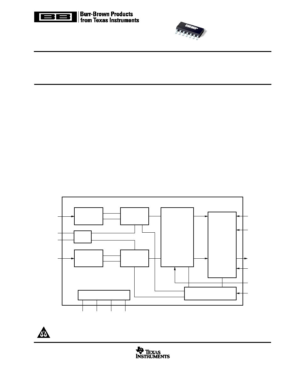
16-Bit, Stereo, Audio
ANALOG-TO-DIGITAL CONVERTER
PCM1801
Clock/Timing Control
BYPAS
V
CC
V
DD
AGND
Reference
Format
Control
FMT
SCKI
Serial Data
Interface
DOUT
BCK
LRCK
V
IN
L
V
REF
1
V
REF
2
V
IN
R
Power Supply
DGND
(≠)
(+)
x1/64
Decimation
and
High-Pass Filter
5th-Order
Modulator
5th-Order
Modulator
PCM1801
(+)
(≠)
Single-Ended-
to-Differential
Converter
Single-Ended-
to-Differential
Converter
www.ti.com
PRODUCTION DATA information is current as of publication date.
Products conform to specifications per the terms of Texas Instruments
standard warranty. Production processing does not necessarily include
testing of all parameters.
Copyright © 1999, Texas Instruments Incorporated
Please be aware that an important notice concerning availability, standard warranty, and use in critical applications of
Texas Instruments semiconductor products and disclaimers thereto appears at the end of this data sheet.
SBAS131A ≠ MAY 2001
q
SYSTEM CLOCK: 256f
S
, 384f
S
, or 512f
S
q
SINGLE +5V POWER SUPPLY
q
SMALL SO-14 PACKAGE
DESCRIPTION
PCM1801 is a low-cost, single chip stereo Analog-to-Digital
Converter (ADC) with single-ended analog voltage inputs.
The PCM1801 uses a delta-sigma modulator with 64x
oversampling, a digital decimation filter, and a serial inter-
face which supports Slave mode operation and two data
formats. The PCM1801 is suitable for a wide variety of cost-
sensitive consumer applications where good performance is
required.
PCM1801
2
SBAS131A
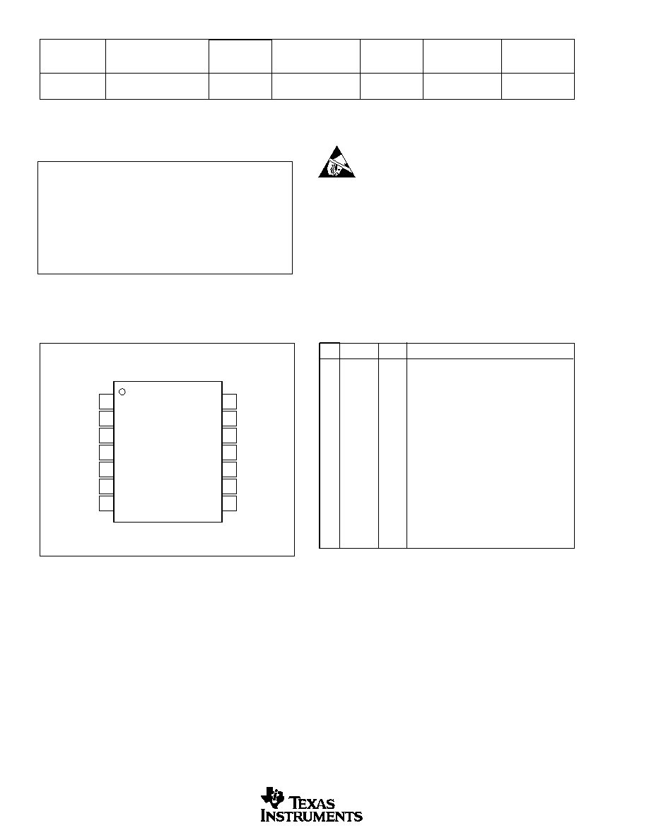
PIN CONFIGURATION
PIN
NAME
I/O
DESCRIPTION
1
V
IN
L
IN
Analog Input, Lch.
2
V
IN
R
IN
Analog Input, Rch.
3
DGND
--
Digital Ground
4
V
DD
--
Digital Power Supply
5
SCKI
IN
System Clock Input; 256f
S
, 384f
S
, or 512f
S
.
6
BCK
IN
Bit Clock Input
7
LRCK
IN
Sampling Clock Input
8
DOUT
OUT
Audio Data Output
9
BYPAS
IN
HPF Bypass Control
(1)
L: HPF Enabled
H: HPF Disabled
10
FMT
IN
Audio Data Format
(1)
L: MSB-First, Left-Justified
H: MSB-First, I
2
S
11
V
CC
--
Analog Power Supply
12
AGND
--
Analog Ground
13
V
REF
2
--
Reference 2 Decoupling Capacitor
14
V
REF
1
--
Reference 1 Decoupling Capacitor
NOTE: (1) With 100k
typical pull-down resistor.
PIN ASSIGNMENTS
Top View
SO
Supply Voltage: +V
DD,
+V
CC
.............................................................. +6.5V
Supply Voltage Differences ...............................................................
±
0.1V
GND Voltage Differences ..................................................................
±
0.1V
Digital Input Voltage ................................................. ≠0.3V to (V
DD
+ 0.3V)
Analog Input Voltage ................................................ ≠0.3V to (V
CC
+ 0.3V)
Input Current (any pin except supplies) ..........................................
±
10mA
Power Dissipation .......................................................................... 300mW
Operating Temperature Range ......................................... ≠25
∞
C to +85
∞
C
Storage Temperature ...................................................... ≠55
∞
C to +125
∞
C
Lead Temperature (soldering, 5s) .................................................. +260
∞
C
(reflow, 10s) ..................................................... +235
∞
C
ABSOLUTE MAXIMUM RATINGS
ELECTROSTATIC
DISCHARGE SENSITIVITY
This integrated circuit can be damaged by ESD. Texas Instru-
ments recommends that all integrated circuits be handled
withappropriate precautions. Failure to observe proper han-
dling and installation procedures can cause damage.
ESD damage can range from subtle performance degradation
to complete device failure. Precision integrated circuits may
be more susceptible to damage because very small parametric
changes could cause the device not to meet its published
specifications.
PACKAGE
SPECIFIED
DRAWING
TEMPERATURE
PACKAGE
ORDERING
TRANSPORT
PRODUCT
PACKAGE
NUMBER
RANGE
MARKING
NUMBER
(1)
MEDIA
PCM1801U
SO-14
235
≠25
∞
C to +85
∞
C
PCM1801U
PCM1801U
Rails
"
"
"
"
"
PCM1801U/2K
Tape and Reel
NOTE: (1) Models with a slash (/) are available only in Tape and Reel in the quantities indicated (e.g., /2K indicates 2000 devices per reel). Ordering 2000 pieces
of "PCM1801U/2K" will get a single 2000-piece Tape and Reel.
PACKAGE/ORDERING INFORMATION
V
IN
L
V
IN
R
DGND
V
DD
SCKI
BCK
LRCK
V
REF
1
V
REF
2
AGND
V
CC
FMT
BYPAS
DOUT
1
2
3
4
5
6
7
14
13
12
11
10
9
8
PCM1801U
PCM1801
3
SBAS131A
ELECTRICAL CHARACTERISTICS
All specifications at +25
∞
C, +V
DD
= +V
CC
= +5V, f
S
= 44.1kHz, and 16-bit data, SYSCLK = 384f
S
, unless otherwise noted.
PCM1801U
PARAMETER
CONDITIONS MIN
TYP MAX UNITS
RESOLUTION
16 Bits
DIGITAL INPUT/OUTPUT
Input Logic Level:
V
IH
(1)
2.0
V
V
IL
(1)
0.8 V
Input Logic Current:
I
IN
(2)
±
1
µ
A
I
IN
(3)
+100
µ
A
Output Logic Level:
V
OH
(4)
I
OH
= ≠1.6mA 4.5
V
V
OL
(4)
I
OL
= +3.2mA
0.5 V
Sampling Frequency
4
44.1 48 kHz
System Clock Frequency
256f
S
1.024
11.2896 12.2880 MHz
384f
S
1.536
16.9344 18.4320 MHz
512f
S
2.024
22.5792 24.5760 MHz
DC ACCURACY
Gain Mismatch Channel-to-Channel
±
1.0
±
2.5 % of FSR
Gain Error
±
2.0
±
5.0 % of FSR
Gain Drift
±
20 ppm of FSR/
∞
C
Bipolar Zero Error
High-Pass Filter Bypass
±
2.0 % of FSR
Bipolar Zero Drift
High-Pass Filter Bypass
±
20 ppm of FSR/
∞
C
DYNAMIC PERFORMANCE
(5)
THD+N at FS (≠0.5dB)
≠88 ≠80 dB
THD+N at ≠60dB
≠90 dB
Dynamic Range
EIAJ, A-weighted 90
93 dB
Signal-To-Noise Ratio
EIAJ, A-weighted 90
93 dB
Channel Separation
88
91 dB
ANALOG INPUT
Input Range
FS (V
IN
= 0dB)
2.828 Vp-p
Center Voltage
2.1 V
Input Impedance
30 k
Anti-Aliasing Filter Frequency Response
≠3dB
170 kHz
DIGITAL FILTER PERFORMANCE
Passband
0.454f
S
Hz
Stopband
0.583f
S
Hz
Passband Ripple
±
0.05 dB
Stopband Attenuation
≠65
dB
Delay Time (Latency)
17.4/f
S
sec
High Pass Frequency Response
≠3dB
0.019f
S
mHz
POWER SUPPLY REQUIREMENTS
Voltage Range
+V
CC
+4.5
+5.0 +5.5 VDC
+V
DD
+4.5
+5.0 +5.5 VDC
Supply Current
(6)
+V
CC
= +V
DD
= +5V
18 25 mA
Power Dissipation
+V
CC
= +V
DD
= +5V
90 125 mW
TEMPERATURE RANGE
Operation
≠25
+85
∞
C
Storage
≠55
+125
∞
C
Thermal Resistance,
JA
100
∞
C/W
NOTES: (1) Pins 5, 6, 7, 9, and 10 (SCKI, BCK, LRCK, BYPAS, FMT). (2) Pins 5, 6, 7 (SCKI, BCK, LRCK) Schmitt-Trigger input. (3) Pins 9, 10 (BYPAS, FMT)
Schmitt-Trigger input with 100k
typical pull-down resistor). (4) Pin 8 (DOUT). (5) f
IN
= 1kHz, using Audio Precisions System II, r ms Mode with 20kHz LPF
and 400Hz HPF enabled. (6) No load on DOUT (pin 8).

PCM1801
4
SBAS131A
BLOCK DIAGRAM
Clock/Timing Control
BYPAS
V
CC
V
DD
AGND
Reference
Format
Control
FMT
SCKI
Serial Data
Interface
DOUT
BCK
LRCK
V
IN
L
V
REF
1
V
REF
2
V
IN
R
Power Supply
DGND
(≠)
(+)
x1/64
Decimation
and
High-Pass Filter
5th-Order
Modulator
5th-Order
Modulator
PCM1801
(+)
(≠)
Single-Ended-
to-Differential
Converter
Single-Ended-
to-Differential
Converter
ANALOG FRONT-END (Single-Channel)
30k
1k
V
IN
L
V
REF
2
1
13
14
1k
Delta-Sigma
Modulator
(+)
(≠)
V
REF
V
REF
1
+
+
1.0
µ
F
4.7
µ
F
+
4.7
µ
F
PCM1801
5
SBAS131A
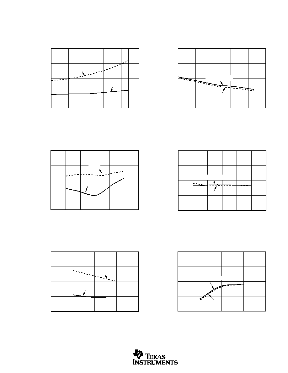
TYPICAL CHARACTERISTICS
At T
A
= +25
∞
C, +V
DD
= +V
CC
= +5V, f
S
= 44.1kHz, and SYSCLK = 384f
S
, unless otherwise noted.
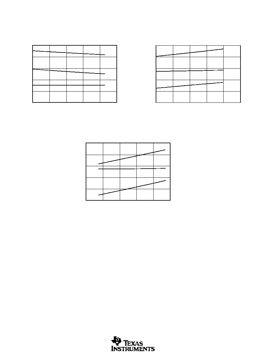
ANALOG DYNAMIC PERFORMANCE
TOTAL HARMONIC DISTORTION + NOISE
vs TEMPERATURE
Temperature (
∞
C)
THD+N at
≠
0.5dB (%)
0.006
0.005
0.004
0.003
0.002
≠25
0
25
50
75
85
100
THD+N at
≠
60dB (%)
3.0
2.8
2.6
2.4
2.2
≠60dB
≠0.5dB
SIGNAL-TO-NOISE RATIO AND DYNAMIC RANGE
vs TEMPERATURE
Temperature (
∞
C)
SNR (dB)
96
95
94
93
92
≠25
0
25
50
75 85
100
Dynamic Range (dB)
96
95
94
93
92
SNR
Dynamic Range
TOTAL HARMONIC DISTORTION + NOISE
vs SUPPLY VOLTAGE
Supply Voltage
(V)
THD+N at
≠
0.5dB (%)
0.006
0.005
0.004
0.003
0.002
4.5
4.75
5.0
5.25
5.5
THD+N at
≠
60dB (%)
3.0
2.8
2.6
2.4
2.2
≠60dB
≠0.5dB
SIGNAL-TO-NOISE RATIO AND DYNAMIC RANGE
vs SUPPLY VOLTAGE
SNR (dB)
96
95
94
93
92
Dynamic Range (dB)
96
95
94
93
92
SNR
Supply Voltage
(V)
4.5
4.75
5.0
5.25
5.5
Dynamic Range
TOTAL HARMONIC DISTORTION + NOISE
vs SAMPLING RATE
Sampling Rate (kHz)
THD+N at
≠
0.5dB (%)
0.006
0.005
0.004
0.003
0.002
32
44.1
48
THD+N at
≠
60dB (%)
3.0
2.8
2.6
2.4
2.2
≠60dB
≠0.5dB
SIGNAL-TO-NOISE RATIO AND DYNAMIC RANGE
vs SAMPLING RATE
Sampling Rate (kHz)
SNR (dB)
96
95
94
93
92
32
44.1
48
Dynamic Range (dB)
96
95
94
93
92
Dynamic Range
SNR
PCM1801
6
SBAS131A
TYPICAL CHARACTERISTICS
(Cont.)
At T
A
= +25
∞
C, +V
DD
= +V
CC
= +5V, f
S
= 44.1kHz, and SYSCLK = 384f
S
, unless otherwise noted.
ANALOG DYNAMIC PERFORMANCE (cont.)
SUPPLY CURRENT vs TEMPERATURE
Temperature (
∞
C)
Supply Current (mA)
20
16
12
8
4
0
≠25
0
25
50
75
100
I
CC
+ I
DD
I
CC
I
DD
SUPPLY CURRENT vs SAMPLING RATE
Sampling Rate (kHz)
Supply Current (mA)
20
16
12
8
4
0
0
10
20
30
40
50
I
CC
I
CC
+ I
DD
I
DD
SUPPLY CURRENT vs SUPPLY VOLTAGE
Supply Voltage (V)
Supply Current (mA)
20
16
12
8
4
0
4.25
4.5
4.75
5.0
5.5
5.75
I
CC
+ I
DD
I
CC
I
DD
PCM1801
7
SBAS131A
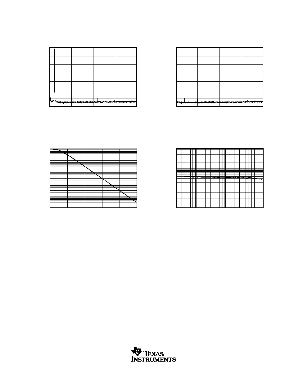
Full-Scale FFT
Frequency (kHz)
Amplitude (dB)
0
≠20
≠40
≠60
≠80
≠100
≠120
≠140
0
5
10
15
20
TYPICAL CHARACTERISTICS
(Cont.)
At T
A
= +25
∞
C, +V
DD
= +V
CC
= +5V, f
S
= 44.1kHz, and SYSCLK = 384f
S
, unless otherwise noted.
OUTPUT SPECTRUM
≠60dBFS FFT
Frequency (kHz)
Amplitude (dB)
0
≠20
≠40
≠60
≠80
≠100
≠120
≠140
0
5
10
15
20
TOTAL HARMONIC DISTORTION + NOISE
vs AMPLITUDE
Amplitude (dBV)
THD+N (%)
100
10
1
0.1
0.01
0.001
≠100
≠80
≠60
≠40
≠20
0
TOTAL HARMONIC DISTORTION + NOISE
vs FREQUENCY
Frequency (Hz)
THD+N (%)
0.1
0.01
0.001
0.0001
20
100
1k
10k
20k
PCM1801
8
SBAS131A
TYPICAL CHARACTERISTICS
(Cont.)
At T
A
= +25
∞
C, +V
DD
= +V
CC
= +5V, f
S
= 44.1kHz, and SYSCLK = 384f
S
, unless otherwise noted.
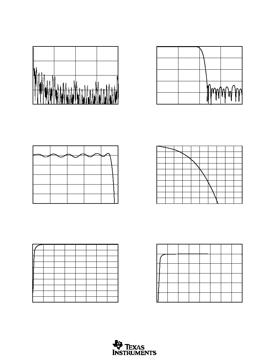
DIGITAL FILTER
OVERALL CHARACTERISTICS
Normalized Frequency (x f
S
Hz)
Amplitude (dB)
0
≠50
≠100
≠150
≠200
8
16
24
32
0
STOPBAND ATTENUATION CHARACTERISTICS
Normalized Frequency (x f
S
Hz)
Amplitude (dB)
0
≠20
≠40
≠60
≠80
≠100
0.25
0.50
0.75
1.00
0
PASSBAND RIPPLE CHARACTERISTICS
Normalized Frequency (x f
S
Hz)
Amplitude (dB)
0.2
0.0
≠0.2
≠0.4
≠0.6
≠0.8
≠1.0
0.1
0.3
0.2
0.4
0.5
0
TRANSITION BAND CHARACTERISTICS
Normalized Frequency (x f
S
Hz)
Amplitude (dB)
0
≠1
≠2
≠3
≠4
≠5
≠6
≠7
≠8
≠9
≠10
0.46 0.47 0.48 0.49 0.50 0.51 0.52 0.53 0.54 0.55
0.45
HIGH PASS FILTER RESPONSE
Normalized Frequency (x f
S
/1000Hz)
Amplitude (dB)
0
≠10
≠20
≠30
≠40
≠50
≠60
≠70
≠80
≠90
≠100
0.1
0.05
0.2
0.15
0.3
0.25
0.4
-0.35
0
HIGH PASS FILTER RESPONSE
Normalized Frequency (x f
S
/1000Hz)
Amplitude (dB)
0.2
0.0
≠0.2
≠0.4
≠0.6
≠0.8
≠1.0
1.0
0.5
2.0
1.5
3.0
2.5
4.0
3.5
0

PCM1801
9
SBAS131A
TYPICAL CHARACTERISTICS
(Cont.)
At T
A
= +25
∞
C, +V
DD
= +V
CC
= +5V, f
S
= 44.1kHz, and SYSCLK = 384f
S
, unless otherwise noted.
ANTI-ALIASING
ANTI-ALIASING FILTER
STOPBAND CHARACTERISTICS
0
≠10
≠20
≠30
≠40
≠50
1
10
100
1k
10k
100k
1M
10M
Frequency (Hz)
Amplitude (dB)
ANTI-ALIASING FILTER
PASSBAND CHARACTERISTICS
0
≠0.2
≠0.4
≠0.6
≠0.8
≠1
1
10
100
1K
10K
100K
Frequency (Hz)
Amplitude (dB)
PCM1801
10
SBAS131A
THEORY OF OPERATION
PCM1801 consists of a bandgap reference, two channels of
a single-to-differential converter, a fully differential 5th-
order delta-sigma modulator, a decimation filter (including
digital high pass), and a serial interface circuit. The Block
Diagram illustrates the total architecture of PCM1801, the
Analog Front-End diagram illustrates the architecture of the
single-to-differential converter, and the anti-aliasing filter is
illustrated in the Block Diagram. Figure 1 illustrates the
architecture of the 5th-order delta-sigma modulator and
transfer functions.
An internal high precision reference with two external capaci-
tors provides all reference voltages which are required by the
converter, and defines the full-scale voltage range of both
channels. The internal single-ended to differential voltage
converter saves the design, space and extra parts needed for
external circuitry required by many delta-sigma converters.
The internal full differential architecture provides a wide
dynamic range and excellent power supply rejection perfor-
mance.
The input signal is sampled at 64x oversampling rate,
eliminating the need for a sample-and-hold circuit, and
simplifying anti-alias filtering requirements. The 5th-order
delta-sigma noise shaper consists of five integrators which
use a switched-capacitor topology, a comparator and a
feedback loop consisting of a 1-bit DAC (Digital-to-Analog
Converter). The delta-sigma modulator shapes the quantiza-
tion noise, shifting it out of the audio band in the frequency
domain. The high order of the modulator enables it to
randomize the modulator outputs, reducing idle tone levels.
The 64f
S
, 1-bit stream from the modulator is converted to
1f
S
, 16-bit digital data by the decimation filter, which also
acts as a low-pass filter to remove the shaped quantization
noise. The DC components are removed by a digital high-
pass filter, and the filtered output is converted to time-
multiplexed serial signals through a serial interface which
provides flexible serial formats.
SYSTEM CLOCK
The system clock for PCM1801 must be either 256f
S
, 384f
S
,
or 512f
S
, where f
S
is the audio sampling frequency. The
system clock must be supplied on SCKI (pin 5).
PCM1801 also has a system clock detection circuit which
automatically senses if the system clock is operating at
256f
S
, 384f
S
, or 512f
S
.
When 384f
S
and 512f
S
system clock are used, the PCM1801
automatically divides these clocks down to 256f
S
internally.
This 256f
S
clock is used to operate the digital filter and the
modulator. Table I lists the relationship of typical sampling
frequencies and system clock frequencies. Figure 2 illus-
trates the system clock timing.
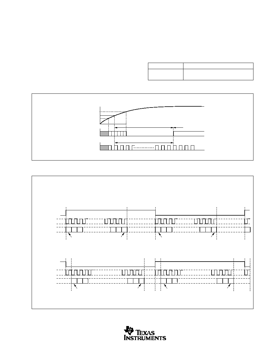
FIGURE 1. Simplified Diagram of the PCM1801 5th-Order Delta-Sigma Modulator.
FIGURE 2. System Clock Timing.
SYSTEM CLOCK FREQUENCY
(MHz)
256f
S
384f
S
512f
S
32
8.1920
12.2880
16.3840
44.1
11.2896
16.9340
22.5792
48
12.2880
18.4320
24.5760
TABLE I. System Clock Frequencies.
SAMPLING RATE FREQUENCY
(kHz)
+
+
≠
+
+
+
5th SW-CAP
Integrator
4th SW-CAP
Integrator
3rd SW-CAP
Integrator
2nd SW-CAP
Integrator
1st SW-CAP
Integrator
+
+
+
+
≠
+
+
≠
1-Bit
DAC
H(z)
Qn(z)
Analog In
X(z)
Digital Out
Y(z)
Y(z) = STF(z) ∑ X(z) + NTF(z) ∑ Qn(z)
Signal Transfer Function
Noise Transfer Function
STF(z) = H(z) / [1 + H(z)]
NTF(z) = 1/ [1 + H(z)]
Comparator
t
CLKIH
System Clock Pulse Width High
t
CLKIH
12ns (min)
System Clock Pulse Width Low
t
CLKIL
12ns (min)
t
CLKIL
SCKI
2.0V
0.8V
PCM1801
11
SBAS131A
RESET
PCM1801 has an internal power-on reset circuit, which ini-
tializes (resets) when the supply voltage (V
CC
/V
DD
) exceeds
4.0V (typ). The PCM1801 stays in the reset state and the
digital output is forced to zero. The digital output is valid after
reset state release and 18436f
S
periods. During reset, the logic
circuits and the digital filter stop operating. Figure 3 illustrates
the internal power-on reset timing.
FIGURE 3. Internal Power-On Reset Timing.
1024 System Clock Periods
Reset
Reset Removal
4.4V
4.0V
3.6V
V
CC
/V
DD
Internal Reset
System Clock
FMT
DATA FORMAT
0 (L)
16-Bit, Left-Justified
1 (H)
16-Bit, I
2
S
TABLE II. Data Format.
FIGURE 4. Audio Data Format.
L≠ch
R≠ch
FMT = L
FMT = H
16-Bit, MSB-First, Left-Justified
MSB
LSB
LRCK
BCK
DOUT
MSB
LSB
1
2
3
14 15 16
14 15 16
1
2
3
1
L-ch
R-ch
16-Bit, MSB-First, I
2
S
MSB
LSB
LRCK
BCK
DOUT
MSB
LSB
1
2
3
14 15 16
1
2
3
14 15 16
SERIAL AUDIO DATA INTERFACE
The PCM1801 interfaces the audio system through BCK (pin
6), LRCK (pin 7), and DOUT (pin 8).
DATA FORMAT
PCM1801 supports two audio data formats in Slave Mode,
and are selected by the FMT control input (pin 10) as shown
in Table II.

PCM1801
12
SBAS131A
SYNCHRONIZATION WITH
DIGITAL AUDIO SYSTEM
PCM1801 operates with LRCK synchronized to the system
clock (SCKI). PCM1801 does not require a specific phase
relationship between LRCK and SCKI, but does require the
synchronization of LRCK and SCKI. If the relationship
between LRCK and SCKI changes more than 6 bit clocks
(BCK) during one sample period due to LRCK or SCKI
jitter, internal operation of the ADC halts within 1/f
S
and the
digital output is forced to BPZ until resynchronization be-
tween LRCK and SCKI is completed. In case of changes less
than 5 bit clocks (BCK), resynchronization does not occur
and above digital output control and discontinuity does not
occur. During undefined data, it may generate some noise in
the audio signal. Also, the transition of normal to undefined
data and undefined or zero data to normal makes a discon-
tinuity of data on the digital output, and may generate some
noise in the audio signal.
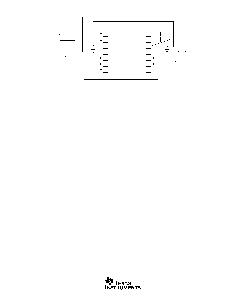
BOARD DESIGN AND LAYOUT
CONSIDERATIONS
V
CC
, V
DD
PINS
The digital and analog power supply lines to the PCM1801
should be bypassed to the corresponding ground pins with both
0.1
µ
F and 10
µ
F capacitors as close to the pins as possible to
maximize the dynamic performance of the ADC. Although
PCM1801 has two power lines to maximize the potential of
dynamic performance, using one common power supply is
recommended to avoid unexpected power supply problems,
such as latch-up due to power supply sequencing.
LRCK
1.4V
1.4V
0.5V
DD
BCK
DOUT
t
BCKH
t
LRCP
t
CKDO
t
LRDO
t
BCKP
t
BCKL
t
LRHD
t
LRSU
DESCRIPTION
SYMBOL
MIN
TYP
MAX
UNITS
BCK Period
t
BCKP
300
ns
BCK Pulse Width HIGH
t
BCKH
120
ns
BCK Pulse Width LOW
t
BCKL
120
ns
LRCK Set Up Time to BCK Rising Edge
t
LRSU
80
ns
LRCK Hold Time to BCK Rising Edge
t
LRHD
40
ns
LRCK Period
t
LRCP
20
µ
s
Delay Time BCK Falling Edge to DOUT Valid
t
CKDO
≠20
40
ns
Delay Time LRCK Edge to DOUT Valid
t
LRDO
≠20
40
ns
Rising Time of All Signals
t
RISE
20
ns
Falling Time of All Signals
t
FALL
20
ns
NOTE: Timing measurement reference level is (V
IH
/V
IL
)/2. Rising and falling time is measured from 10% to
90% of I/O signals' swing. Load capacitance of DOUT signal is 20pF.
FIGURE 5. Audio Data Interface Timing.
AGND, DGND PINS
To maximize the dynamic performance of the PCM1801,
the analog and digital grounds are not internally connected.
These points should have very low impedance to avoid
digital noise feedback into the analog ground. They should
be connected directly to each other under the PCM1801
package to reduce potential noise problems.
V
IN
PINS
A 1.0
µ
F tantalum capacitor is recommended as an AC-
coupling capacitor which establishes a 5.3Hz cut-off fre-
quency. If a higher full-scale input voltage is required, the
input voltage range can be increased by adding a series
resistor to the V
IN
pins.
V
REF
INPUTS
A 4.7
µ
F tantalum capacitor is recommended between the
V
REF
1, V
REF
2, and AGND references to ensure low source
impedance. These capacitors should be located as close as
possible to the V
REF
1 or V
REF
2 pins to reduce dynamic errors
on the ADC's references.
SYSTEM CLOCK
The quality of the system clock can influence dynamic
performance in the PCM1801. The duty cycle, jitter, and
threshold voltage at the system clock input pin must be
carefully managed. When power is supplied to the part, the
system clock, bit clock (BCK), and word clock (LRCK)
should also be supplied simultaneously. Failure to supply
the audio clocks will result in a power dissipation increase
of up to three times normal dissipation and may degrade
long-term reliability if the maximum power dissipation limit
is exceeded.
PCM1801
13
SBAS131A
1
2
3
4
5
6
7
V
IN
L
V
IN
R
DGND
V
DD
SCKI
BCK
LRCK
V
REF
1
V
REF
2
AGND
V
CC
FMT
BYPAS
DOUT
14
13
12
11
10
9
8
System Clock
Data Clock
Latch Enable
Data Out
+
C
1
(1)
+
C
2
(1)
C
3
(2)
+
C
6
(3)
+
C
5
(3)
C
4
(2)
0V
+5V
Format
Bypass
Audio Data
Processor
Pin Program
or Control
Lch IN
Rch IN
NOTES: (1) C1 and C2: A 1
µ
F capacitor gives 5.3Hz (
= 1
µ
F * 30k
) cut-off frequency for input HPF in
normal operation and requires power-on setting time of 6ms at power up. (2) C3 and C4: Bypass
capacitor 0.1
µ
F ceramic and 30
µ
F tantalum or aluminum electrolytic, depending on layout and power
supply. (3) C5 and C6: 4.7
µ
F tantalum or aluminum electrolytic capacitor.
FIGURE 6. Typical Circuit Connection.

PACKAGING INFORMATION
ORDERABLE DEVICE
STATUS(1)
PACKAGE TYPE
PACKAGE DRAWING
PINS
PACKAGE QTY
PCM1801U
ACTIVE
SOIC
D
14
56
PCM1801U/2K
ACTIVE
SOIC
D
14
2000
(1) The marketing status values are defined as follows:
ACTIVE: Product device recommended for new designs.
LIFEBUY: TI has announced that the device will be discontinued, and a lifetime-buy period is in effect.
NRND: Not recommended for new designs. Device is in production to support existing customers, but TI does not recommend using this part in
a new design.
PREVIEW: Device has been announced but is not in production. Samples may or may not be available.
OBSOLETE: TI has discontinued the production of the device.
PACKAGE OPTION ADDENDUM
www.ti.com
3-Oct-2003

IMPORTANT NOTICE
Texas Instruments Incorporated and its subsidiaries (TI) reserve the right to make corrections, modifications,
enhancements, improvements, and other changes to its products and services at any time and to discontinue
any product or service without notice. Customers should obtain the latest relevant information before placing
orders and should verify that such information is current and complete. All products are sold subject to TI's terms
and conditions of sale supplied at the time of order acknowledgment.
TI warrants performance of its hardware products to the specifications applicable at the time of sale in
accordance with TI's standard warranty. Testing and other quality control techniques are used to the extent TI
deems necessary to support this warranty. Except where mandated by government requirements, testing of all
parameters of each product is not necessarily performed.
TI assumes no liability for applications assistance or customer product design. Customers are responsible for
their products and applications using TI components. To minimize the risks associated with customer products
and applications, customers should provide adequate design and operating safeguards.
TI does not warrant or represent that any license, either express or implied, is granted under any TI patent right,
copyright, mask work right, or other TI intellectual property right relating to any combination, machine, or process
in which TI products or services are used. Information published by TI regarding third-party products or services
does not constitute a license from TI to use such products or services or a warranty or endorsement thereof.
Use of such information may require a license from a third party under the patents or other intellectual property
of the third party, or a license from TI under the patents or other intellectual property of TI.
Reproduction of information in TI data books or data sheets is permissible only if reproduction is without
alteration and is accompanied by all associated warranties, conditions, limitations, and notices. Reproduction
of this information with alteration is an unfair and deceptive business practice. TI is not responsible or liable for
such altered documentation.
Resale of TI products or services with statements different from or beyond the parameters stated by TI for that
product or service voids all express and any implied warranties for the associated TI product or service and
is an unfair and deceptive business practice. TI is not responsible or liable for any such statements.
Following are URLs where you can obtain information on other Texas Instruments products and application
solutions:
Products
Applications
Amplifiers
amplifier.ti.com
Audio
www.ti.com/audio
Data Converters
dataconverter.ti.com
Automotive
www.ti.com/automotive
DSP
dsp.ti.com
Broadband
www.ti.com/broadband
Interface
interface.ti.com
Digital Control
www.ti.com/digitalcontrol
Logic
logic.ti.com
Military
www.ti.com/military
Power Mgmt
power.ti.com
Optical Networking
www.ti.com/opticalnetwork
Microcontrollers
microcontroller.ti.com
Security
www.ti.com/security
Telephony
www.ti.com/telephony
Video & Imaging
www.ti.com/video
Wireless
www.ti.com/wireless
Mailing Address:
Texas Instruments
Post Office Box 655303 Dallas, Texas 75265
Copyright
2003, Texas Instruments Incorporated