www.ti.com
FEATURES
APPLICATIONS
DESCRIPTION
PCM1803A
SLES142A ≠ JUNE 2005 ≠ REVISED AUGUST 2006
SINGLE-ENDED, ANALOG-INPUT 24-BIT, 96-kHz STEREO A/D CONVERTER
∑
AV Amplifier Receiver
∑
24-Bit Delta-Sigma Stereo A/D Converter
∑
MD Player
∑
Single-Ended Voltage Input: 3 Vp-p
∑
CD Recorder
∑
Oversampling Decimation Filter:
∑
Multitrack Receiver
≠ Oversampling Frequency: ◊64, ◊128
∑
Electric Musical Instrument
≠ Pass-Band Ripple: ±0.05 dB
≠ Stop-Band Attenuation: ≠65 dB
≠ On-Chip High-Pass Filter: 0.84 Hz (44.1 kHz)
The
PCM1803A
is
high-performance,
low-cost,
∑
High-Performance:
single-chip stereo analog-to-digital converter with
≠ THD+N: ≠95 dB (Typically)
single-ended analog voltage input. The PCM1803A
uses a delta-sigma modulator with 64- and 128-times
≠ SNR: 103 dB (Typically)
oversampling, and includes a digital decimation filter
≠ Dynamic Range: 103 dB (Typically)
and
high-pass
filter,
which
removes
the
dc
∑
PCM Audio Interface:
component
of
the
input
signal.
For
various
applications, the PCM1803A supports master and
≠ Master/Slave Mode Selectable
slave modes and four data formats in serial interface.
≠ Data Formats:
The PCM1803A is suitable for a wide variety of
∑
24-Bit Left-Justified
cost-sensitive consumer applications where good
performance and operation from a 5-V analog supply
∑
24-Bit I
2
S
and
3.3-V
digital
supply
are
required.
The
∑
20-, 24-Bit Right-Justified
PCM1803A is fabricated using a highly advanced
∑
Sampling Rate: 16 kHz to 96 kHz
CMOS process and is available in a small 20-pin
SSOP package.
∑
System Clock: 256 f
S
, 384 f
S
, 512 f
S
, 768 f
S
∑
Dual Power Supplies: 5 V for Analog, 3.3 V
for Digital
∑
Package: 20-Pin SSOP
Please be aware that an important notice concerning availability, standard warranty, and use in critical applications of Texas
Instruments semiconductor products and disclaimers thereto appears at the end of this data sheet.
System Two, Audio Precision are trademarks of Audio Precision, Inc.
All other trademarks are the property of their respective owners.
PRODUCTION DATA information is current as of publication date.
Copyright © 2005≠2006, Texas Instruments Incorporated
Products conform to specifications per the terms of the Texas
Instruments standard warranty. Production processing does not
necessarily include testing of all parameters.

www.ti.com
PIN ASSIGNMENTS
1
2
3
4
5
6
7
8
9
10
20
19
18
17
16
15
14
13
12
11
V
IN
L
V
IN
R
V
REF
1
V
REF
2
V
CC
AGND
PDWN
BYPAS
TEST
LRCK
MODE1
MODE0
FMT1
FMT0
OSR
SCKI
V
DD
DGND
DOUT
BCK
PCM1803A
(TOP VIEW)
P0009-03
BLOCK DIAGRAM
BCK
V
IN
L
Reference
V
REF
1
V
REF
2
V
IN
R
Delta-Sigma
Modulator
Delta-Sigma
Modulator
◊
1/64 ,
◊
1/128
Decimation
Filter
With
High-Pass Filter
Power Supply
AGND
V
CC
V
DD
DGND
Clock and Timing Control
Serial
Interface
Mode/
Format
Control
LRCK
DOUT
FMT0
FMT1
MODE0
MODE1
BYPAS
OSR
PDWN
SCKI
B0004-06
TEST
PCM1803A
SLES142A ≠ JUNE 2005 ≠ REVISED AUGUST 2006
This integrated circuit can be damaged by ESD. Texas Instruments recommends that all integrated circuits be handled with
appropriate precautions. Failure to observe proper handling and installation procedures can cause damage.
ESD damage can range from subtle performance degradation to complete device failure. Precision integrated circuits may be
more susceptible to damage because very small parametric changes could cause the device not to meet its published
specifications.
2
Submit Documentation Feedback
www.ti.com
DEVICE INFORMATION
ABSOLUTE MAXIMUM RATINGS
PCM1803A
SLES142A ≠ JUNE 2005 ≠ REVISED AUGUST 2006
TERMINAL FUNCTIONS
TERMINAL
I/O
DESCRIPTION
NAME
NO.
AGND
6
≠
Analog GND
BCK
11
I/O
Audio data bit clock input/output
(1)
BYPAS
8
I
HPF bypass control. LOW: Normal mode (dc reject); HIGH: Bypass mode (through)
(2)
DGND
13
≠
Digital GND
DOUT
12
O
Audio data digital output
FMT0
17
I
Audio data format select input 0. See Data Format section.
(2)
FMT1
18
I
Audio data format select input 1. See Data Format section.
(2)
LRCK
10
I/O
Audio data latch enable input/output
(1)
MODE0
19
I
Mode select input 0. See Data Format section.
(2)
MODE1
20
I
Mode select input 1. See Data Format section.
(2)
OSR
16
I
Oversampling ratio select input. LOW: ◊64 f
S
, HIGH: ◊128 f
S
(2)
PDWN
7
I
Power-down control, active-low
(2)
SCKI
15
I
System clock input: 256 f
S
, 384 f
S
, 512 f
S
, or 768 f
S
(3)
TEST
9
I
Test, must be connected to DGND
(2)
V
CC
5
≠
Analog power supply, 5-V
V
DD
14
≠
Digital power supply, 3.3-V
V
IN
L
1
I
Analog input, L-channel
V
IN
R
2
I
Analog input, R-channel
V
REF
1
3
≠
Reference-voltage-1 decoupling capacitor
V
REF
2
4
≠
Reference-voltage-2 decoupling capacitor
(1)
Schmitt-trigger input
(2)
Schmitt-trigger input with internal pulldown (50 k
, typically), 5-V tolerant
(3)
Schmitt-trigger input, 5-V tolerant
over operating free-air temperature range (unless otherwise noted)
(1)
Supply voltage
V
CC
≠0.3 V to 6.5 V
Supply voltage
V
DD
≠0.3 V to 4 V
Ground voltage differences
AGND, DGND
±
0.1 V
Digital input voltage, V
I
LRCK, BCK, DOUT
≠0.3 V to (V
DD
+ 0.3 V) < 4 V
Digital input voltage, V
I
PDWN, BYPAS, TEST, SCKI, OSR, FMT0,
≠0.3 V to 6.5 V
FMT1, MODE0, MODE1
Analog input voltage, V
I
V
IN
L, V
IN
R, V
REF
1, V
REF
2
≠0.3 V to (V
CC
+ 0.3 V) < 6.5 V
Input current, I
I
Any pins except supplies
±
10 mA
Ambient temperature under bias, T
bias
≠40∞C to 125∞C
Storage temperature, T
stg
≠55∞C to 150∞C
Junction temperature, T
J
150∞C
Lead temperature (soldering)
260∞C, 5 s
Package temperature (IR reflow, peak)
260∞C
(1)
Stresses beyond those listed under "absolute maximum ratings" may cause permanent damage to the device. These are stress ratings
only and functional operation of the device at these or any other conditions beyond those indicated under "recommended operating
conditions" is not implied. Exposure to absolute-maximum-rated conditions for extended periods may affect device reliability.
3
Submit Documentation Feedback
www.ti.com
RECOMMENDED OPERATING CONDITIONS
ELECTRICAL CHARACTERISTICS
PCM1803A
SLES142A ≠ JUNE 2005 ≠ REVISED AUGUST 2006
over operating free-air temperature range
MIN
NOM
MAX
UNIT
Analog supply voltage, V
CC
4.5
5
5.5
V
Digital supply voltage, V
DD
2.7
3.3
3.6
V
Analog input voltage, full-scale (≠0 dB)
3
Vp-p
Digital input logic family
TTL
System clock
8.192
49.152
MHz
Digital input clock frequency
Sampling clock
32
96
kHz
Digital output load capacitance
20
pF
Operating free-air temperature, T
A
≠25
85
∞C
All specifications at T
A
= 25∞C, V
CC
= 5 V, V
DD
= 3.3 V, master mode, f
S
= 44.1 kHz, system clock = 384 f
S
,
oversampling ratio = ◊128, 24-bit data (unless otherwise noted)
PARAMETER
TEST CONDITIONS
MIN
TYP
MAX
UNIT
Resolution
24
Bits
DATA FORMAT
Audio data interface format
Left-justified, I
2
S, right-justified
Audio data bit length
20, 24
Bits
Audio data format
MSB-first, 2s complement
f
S
Sampling frequency
16
44.1
96
kHz
256 f
S
4.096
11.2896
24.576
384 f
S
6.144
16.9344
36.864
System clock frequency
MHz
512 f
S
8.192
22.5792
49.152
768 f
S
12.288
33.8688
≠
INPUT LOGIC
V
IH
(1)
2
V
DD
V
IL
(1)
0
0.8
Input logic-level voltage
Vdc
V
IH
(2) (3)
2
5.5
V
IL
(2) (3)
0
0.8
I
IH
(1) (2)
V
IN
= V
DD
±
10
I
IL
(1) (2)
V
IN
= 0
±
10
Input logic-level current
µ
A
I
IH
(3)
V
IN
= V
DD
65
100
I
IL
(3)
V
IN
= 0
±
10
OUTPUT LOGIC
V
OH
(4)
I
OUT
= ≠4 mA
2.8
Output logic-level voltage
Vdc
V
OL
(4)
I
OUT
= 4 mA
0.5
DC ACCURACY
Gain mismatch, channel-to-channel
±
1
±
3
% of FSR
Gain error
±
2
±
4
% of FSR
Bipolar zero error
HPF bypass
±
0.4
% of FSR
(1)
Pins 10≠11: LRCK, BCK (Schmitt-trigger input, in slave mode)
(2)
Pin 15: SCKI (Schmitt-trigger input, 5-V tolerant)
(3)
Pins 7≠9, 16≠20: PDWN, BYPAS, TEST, OSR, FMT0, FMT1, MODE0, MODE1 (Schmitt-trigger input, with 50-k
typical pulldown
resistor, 5-V tolerant)
(4)
Pins 10≠12: LRCK, BCK (in master mode), DOUT
4
Submit Documentation Feedback
www.ti.com
PCM1803A
SLES142A ≠ JUNE 2005 ≠ REVISED AUGUST 2006
ELECTRICAL CHARACTERISTICS (continued)
All specifications at T
A
= 25∞C, V
CC
= 5 V, V
DD
= 3.3 V, master mode, f
S
= 44.1 kHz, system clock = 384 f
S
,
oversampling ratio = ◊128, 24-bit data (unless otherwise noted)
PARAMETER
TEST CONDITIONS
MIN
TYP
MAX
UNIT
DYNAMIC PERFORMANCE
(5)
V
IN
= ≠0.5 dB, f
S
= 44.1 kHz
≠95
≠89
V
IN
= ≠0.5 dB, f
S
= 96 kHz
(6)
≠93
THD+N
Total harmonic distortion + noise
dB
V
IN
= ≠60 dB, f
S
= 44.1 kHz
≠41
V
IN
= ≠60 dB, f
S
= 96 kHz
(6)
≠41
f
S
= 44.1 kHz, A-weighted
100
103
Dynamic range
dB
f
S
= 96 kHz, A-weighted
(6)
103
f
S
= 44.1 kHz, A-weighted
100
103
SNR
Signal-to-noise ratio
dB
f
S
= 96 kHz, A-weighted
(6)
103
f
S
= 44.1 kHz
95
98
Channel separation
dB
f
S
= 96 kHz
(6)
99
ANALOG INPUT
V
I
Input voltage
0.6 V
CC
Vp-p
Center voltage (V
REF
1)
0.5 V
CC
V
Input impedance
40
k
DIGITAL FILTER PERFORMANCE
Pass band
0.454 f
S
Hz
Stop band
0.583 f
S
Hz
Pass-band ripple
±
0.05
dB
Stop-band attenuation
≠65
dB
t
GD
Group delay time
17.4/f
S
s
HPF frequency response
≠3 dB
0.019 f
S
mHz
POWER SUPPLY REQUIREMENTS
V
CC
4.5
5
5.5
Vdc
Supply voltage range
V
DD
2.7
3.3
3.6
Vdc
7.7
10
mA
I
CC
Power down
(8)
5
µ
A
Supply current
(7)
f
S
= 44.1 kHz
6.5
9
mA
I
DD
f
S
= 96 kHz
(6)
11.7
mA
Power down
(8)
1
µ
A
f
S
= 44.1 kHz
60
80
mW
Power dissipation
f
S
= 96 kHz
(6)
77
mW
Power down
(8)
28
µ
W
TEMPERATURE RANGE
T
A
Operating free-air temperature
≠40
85
∞C
JA
Thermal resistance
20-pin SSOP
115
∞C/W
(5)
Analog performance specifications are tested using the System TwoTM audio measurement system by Audio PrecisionTM, using 400-Hz
HPF, 20-kHz LPF in rms mode.
(6)
f
S
= 96 kHz, system clock = 256 f
S
, oversampling ratio = ◊64.
(7)
Minimum load on DOUT (pin 12), BCK (pin 11), LRCK (pin 10)
(8)
Halt SCKI, BCK, LRCK
5
Submit Documentation Feedback
www.ti.com
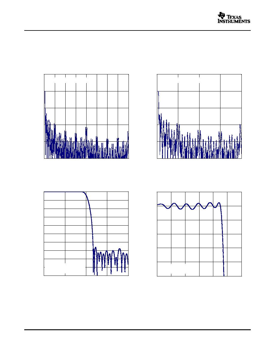
TYPICAL PERFORMANCE CURVES OF INTERNAL FILTER
Decimation Filter Frequency Response
Normalized Frequency [
◊
f
S
]
-200
-150
-100
-50
0
50
0
8
16
24
32
40
48
56
64
Oversampling Ratio =
y
128
Amplitude - dB
G001
G002
Normalized Frequency [
◊
f
S
]
-200
-150
-100
-50
0
50
0
8
16
24
32
Amplitude - dB
Oversampling Ratio =
y
64
G003
Normalized Frequency [
◊
f
S
]
-100
-90
-80
-70
-60
-50
-40
-30
-20
-10
0
0.00
0.25
0.50
0.75
1.00
Amplitude - dB
Oversampling
Ratio =
y
128 and
y
64
G004
Normalized Frequency [
◊
f
S
]
-1.0
-0.8
-0.6
-0.4
-0.2
0.0
0.2
0.0
0.1
0.2
0.3
0.4
0.5
0.6
Amplitude - dB
Oversampling
Ratio =
y
128 and
y
64
PCM1803A
SLES142A ≠ JUNE 2005 ≠ REVISED AUGUST 2006
All specifications at T
A
= 25∞C, V
CC
= 5 V, V
DD
= 3.3 V, master mode, f
S
= 44.1 kHz, system clock = 384 f
S
,
oversampling ratio = ◊128, 24-bit data (unless otherwise noted)
OVERALL CHARACTERISTICS
OVERALL CHARACTERISTICS
Figure 1.
Figure 2.
STOP-BAND ATTENUATION CHARACTERISTICS
PASS-BAND RIPPLE CHARACTERISTICS
Figure 3.
Figure 4.
6
Submit Documentation Feedback
www.ti.com
LOW-CUT FILTER FREQUENCY RESPONSE
G005
Normalized Frequency [
◊
f
S
/1000]
-100
-90
-80
-70
-60
-50
-40
-30
-20
-10
0
0.0
0.1
0.2
0.3
0.4
Amplitude - dB
G006
Normalized Frequency [
◊
f
S
/1000]
-1.0
-0.8
-0.6
-0.4
-0.2
0.0
0.2
0
1
2
3
4
Amplitude - dB
PCM1803A
SLES142A ≠ JUNE 2005 ≠ REVISED AUGUST 2006
TYPICAL PERFORMANCE CURVES OF INTERNAL FILTER (continued)
All specifications at T
A
= 25∞C, V
CC
= 5 V, V
DD
= 3.3 V, master mode, f
S
= 44.1 kHz, system clock = 384 f
S
,
oversampling ratio = ◊128, 24-bit data (unless otherwise noted)
HPF STOP-BAND CHARACTERISTICS
HPF PASS-BAND CHARACTERISTICS
Figure 5.
Figure 6.
7
Submit Documentation Feedback
www.ti.com
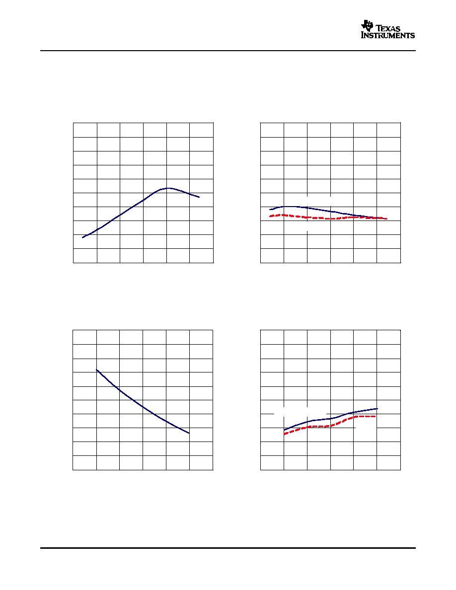
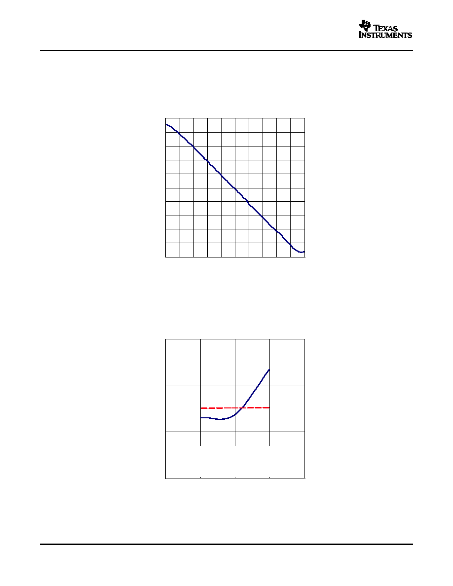
TYPICAL PERFORMANCE CURVES
G007
-100
-99
-98
-97
-96
-95
-94
-93
-92
-91
-90
-50
-25
0
25
50
75
100
T
A
- Free-Air Temperature -
∞
C
THD+N - T
otal Harmonic Distortion + Noise - dB
100
101
102
103
104
105
106
107
108
109
110
-50
-25
0
25
50
75
100
G008
T
A
- Free-Air Temperature -
∞
C
Dynamic Range and SNR - dB
SNR
Dynamic Range
-100
-99
-98
-97
-96
-95
-94
-93
-92
-91
-90
4.25
4.50
4.75
5.00
5.25
5.50
5.75
V
CC
- Supply Voltage - V
THD+N - T
otal Harmonic Distortion + Noise - dB
G009
G010
100
101
102
103
104
105
106
107
108
109
110
4.25
4.50
4.75
5.00
5.25
5.50
5.75
V
CC
- Supply Voltage - V
Dynamic Range and SNR - dB
SNR
Dynamic Range
PCM1803A
SLES142A ≠ JUNE 2005 ≠ REVISED AUGUST 2006
All specifications at T
A
= 25∞C, V
CC
= 5 V, V
DD
= 3.3 V, master mode, f
S
= 44.1 kHz, system clock = 384 f
S
,
oversampling ratio = ◊128, 24-bit data (unless otherwise noted)
TOTAL HARMONIC DISTORTION + NOISE
DYNAMIC RANGE and SIGNAL-TO-NOISE RATIO
vs
vs
TEMPERATURE
TEMPERATURE
Figure 7.
Figure 8.
TOTAL HARMONIC DISTORTION + NOISE
DYNAMIC RANGE and SIGNAL-TO-NOISE RATIO
vs
vs
SUPPLY VOLTAGE
SUPPLY VOLTAGE
Figure 9.
Figure 10.
8
Submit Documentation Feedback

www.ti.com
-100
-99
-98
-97
-96
-95
-94
-93
-92
-91
-90
0
10
20
30
40
f
SAMPLE
Condition - kHz
THD+N - T
otal Harmonic Distortion + Noise - dB
44.1
96
(2)
48
(1)
(1)
f
S
= 48 kHz, System Clock = 256 f
S
,
Oversampling Ratio =
◊
128.
(2)
f
S
= 96 kHz, System Clock = 256 f
S
,
Oversampling Ratio =
◊
64.
G011
100
101
102
103
104
105
106
107
108
109
110
0
10
20
30
40
Dynamic Range and SNR - dB
44.1
96
(2)
48
(1)
SNR
Dynamic Range
f
SAMPLE
Condition - kHz
(1)
f
S
= 48 kHz, System Clock = 256 f
S
,
Oversampling Ratio =
◊
128.
(2)
f
S
= 96 kHz, System Clock = 256 f
S
,
Oversampling Ratio =
◊
64.
G012
OUTPUT SPECTRUM
G013
f - Frequency - kHz
-140
-120
-100
-80
-60
-40
-20
0
0
5
10
15
20
Input Level = -0.5 dB
Data Points = 8192
Amplitude - dB
G014
f - Frequency - kHz
-140
-120
-100
-80
-60
-40
-20
0
0
5
10
15
20
Amplitude - dB
Input Level = -60 dB
Data Points = 8192
PCM1803A
SLES142A ≠ JUNE 2005 ≠ REVISED AUGUST 2006
TYPICAL PERFORMANCE CURVES (continued)
All specifications at T
A
= 25∞C, V
CC
= 5 V, V
DD
= 3.3 V, master mode, f
S
= 44.1 kHz, system clock = 384 f
S
,
oversampling ratio = ◊128, 24-bit data (unless otherwise noted)
TOTAL HARMONIC DISTORTION + NOISE
DYNAMIC RANGE and SIGNAL-TO-NOISE RATIO
vs
vs
f
SAMPLE
CONDITION
f
SAMPLE
CONDITION
Figure 11.
Figure 12.
OUTPUT SPECTRUM
OUTPUT SPECTRUM
Figure 13.
Figure 14.
9
Submit Documentation Feedback
www.ti.com
-100
-90
-80
-70
-60
-50
-40
-30
-20
-10
0
-100 -90 -80 -70 -60 -50 -40 -30 -20 -10
0
Signal Level - dB
THD+N - T
otal Harmonic Distortion + Noise - dB
G015
SUPPLY CURRENT
0
5
10
15
0
10
20
30
40
I
C
C
and I
D
D
- Supply Current - mA
44.1
96
(2)
48
(1)
I
CC
f
SAMPLE
Condition - kHz
I
DD
(1)
f
S
= 48 kHz, System Clock = 256 f
S
,
Oversampling Ratio =
◊
128.
(2)
f
S
= 96 kHz, System Clock = 256 f
S
,
Oversampling Ratio =
◊
64.
G016
PCM1803A
SLES142A ≠ JUNE 2005 ≠ REVISED AUGUST 2006
TYPICAL PERFORMANCE CURVES (continued)
All specifications at T
A
= 25∞C, V
CC
= 5 V, V
DD
= 3.3 V, master mode, f
S
= 44.1 kHz, system clock = 384 f
S
,
oversampling ratio = ◊128, 24-bit data (unless otherwise noted)
TOTAL HARMONIC DISTORTION + NOISE
vs
SIGNAL LEVEL
Figure 15.
SUPPLY CURRENT
vs
f
SAMPLE
CONDITION
Figure 16.
10
Submit Documentation Feedback
www.ti.com
DEVICE INFORMATION
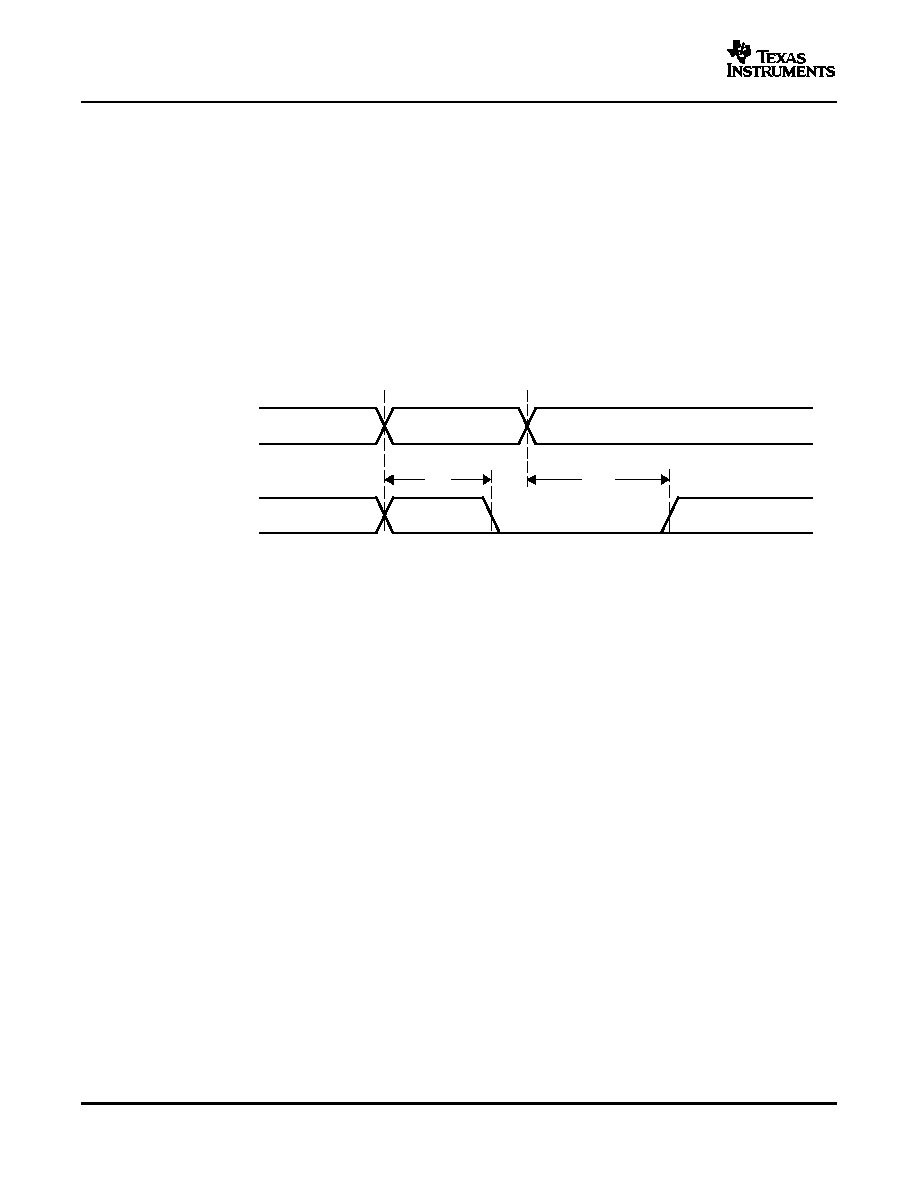
SYSTEM CLOCK
SCKI
0.8 V
SCKI
2 V
t
w(SCKL)
t
w(SCKH)
T0005B07
POWER-ON-RESET SEQUENCE
PCM1803A
SLES142A ≠ JUNE 2005 ≠ REVISED AUGUST 2006
The PCM1803A supports 256 f
S
, 384 f
S
, 512 f
S
, and 768 f
S
as the system clock, where f
S
is the audio sampling
frequency. The system clock must be supplied on SCKI (pin 15).
The PCM1803A has a system clock-detection circuit that automatically senses if the system clock is operating at
256 f
S
, 384 f
S
, 512 f
S
, or 768 f
S
in slave mode. In master mode, the system clock frequency must be selected by
MODE0 (pin 19) and MODE1 (pin 20), and 768 f
S
is not available. The system clock is divided automatically into
128 f
S
and 64 f
S
, and these frequencies are used to operate the digital filter and the delta-sigma modulator.
Table 1
shows the relationship of typical sampling frequency and system clock frequency, and
Figure 17
shows
system clock timing.
Table 1. Sampling Frequency and System Clock Frequency
SYSTEM CLOCK FREQUENCY (MHz)
SAMPLING FREQUENCY (kHz)
256 f
S
384 f
S
512 f
S
768 f
S
(1)
32
8.1920
12.2880
16.3840
24.5760
44.1
11.2896
16.9344
22.5792
33.8688
48
12.2880
18.4320
24.5760
36.8640
64
16.3840
24.5760
32.7680
49.1520
88.2
22.5792
33.8688
45.1584
≠
96
24.5760
36.8640
49.1520
≠
(1)
Slave mode only
SYMBOL
PARAMETER
MIN
MAX
UNIT
t
w(SCKH)
System clock pulse duration, HIGH
8
ns
t
w(SCKL)
System clock pulse duration, LOW
8
ns
Figure 17. System Clock Timing
The PCM1803A has an internal power-on-reset circuit, and initialization (reset) is performed automatically at the
time when power-supply voltage (V
DD
) exceeds 2.2 V (typical). While V
DD
< 2.2 V (typical) and for 1024 system
clock cycles after V
DD
> 2.2 V (typical), the PCM1803A stays in the reset state, and the digital output is forced to
zero. The digital output becomes valid when a time period of 4480/f
S
has elapsed following release from the
reset state.
Figure 18
illustrates the internal power-on-reset timing and the digital output for power-on reset.
11
Submit Documentation Feedback

www.ti.com
System Clock
2.6 V
2.2 V
1.8 V
Internal Reset
DOUT
Zero Data
Normal Data
Reset
V
DD
Reset Removal
1024 System Clocks
4480 / f
S
T0014-05
SERIAL AUDIO DATA INTERFACE
INTERFACE MODE
DATA FORMAT
PCM1803A
SLES142A ≠ JUNE 2005 ≠ REVISED AUGUST 2006
Figure 18. Internal Power-On-Reset Timing
The PCM1803A interfaces the audio system through BCK (pin 11), LRCK (pin 10), and DOUT (pin 12).
The PCM1803A supports master mode and slave mode as interface modes, and they are selected by MODE1
(pin 20) and MODE0 (pin 19) as shown in
Table 2
.
In master mode, the PCM1803A provides the timing of serial audio data communications between the
PCM1803A and the digital audio processor or external circuit. While in slave mode, the PCM1803A receives the
timing for data transfers from an external controller.
Table 2. Interface Mode
MODE1
MODE0
INTERFACE MODE
0
0
Slave mode (256 f
S
, 384 f
S
, 512 f
S
, 768 f
S
)
0
1
Master mode (512 f
S
)
1
0
Master mode (384 f
S
)
1
1
Master mode (256 f
S
)
Master Mode
In master mode, BCK and LRCK work as output pins, and these pins are controlled by timing, which is
generated in the clock circuit of the PCM1803A. The frequency of BCK is fixed at LRCK ◊ 64. The 768-f
S
system
clock is not available in master mode.
Slave Mode
In slave mode, BCK and LRCK work as input pins. The PCM1803A accepts the 64-BCK/LRCK or 48-BCK/LRCK
format (only for 384 f
S
and 768 f
S
system clocks), not the 32-BCK/LRCK format.
The PCM1803A supports four audio data formats in both master and slave modes, and the data formats are
selected by FMT1 (pin 18) and FMT0 (pin 17) as shown in
Table 3
.
Figure 19
illustrates the data formats in
slave and master modes.
12
Submit Documentation Feedback
www.ti.com
LRCK
Right-Channel
Left-Channel
BCK
DOUT
24
22 23 24
3
2
1
MSB
LSB
22 23 24
3
2
1
MSB
LSB
LRCK
Right-Channel
Left-Channel
BCK
DOUT
20
18 19 20
3
2
1
MSB
LSB
18 19 20
3
2
1
MSB
LSB
LRCK
Right-Channel
Left-Channel
BCK
DOUT
22 23 24
3
2
1
MSB
LSB
22 23 24
3
2
1
MSB
LSB
BCK
LRCK
Right-Channel
Left-Channel
DOUT
1
22 23 24
3
2
1
MSB
LSB
22 23 24
3
2
1
MSB
LSB
24-Bit, MSB-First, Left-Justified
FORMAT 0: FMT[1:0] = 00
24-Bit, MSB-First, I
2
S
FORMAT 1: FMT[1:0] = 01
24-Bit, MSB-First, Right-Justified
FORMAT 2: FMT[1:0] = 10
20-Bit, MSB-First, Right-Justified
FORMAT 3: FMT[1:0] = 11
T0016-11
PCM1803A
SLES142A ≠ JUNE 2005 ≠ REVISED AUGUST 2006
Table 3. Data Formats
FORMAT
FMT1
FMT0
DESCRIPTION
0
0
0
Left-justified, 24-bit
1
0
1
I
2
S, 24-bit
2
1
0
Right-justified, 24-bit
3
1
1
Right-justified, 20-bit
Figure 19. Audio Data Formats (LRCK and BCK Work as Inputs in Slave Mode and as Outputs in Master
Mode)
13
Submit Documentation Feedback
www.ti.com
INTERFACE TIMING
BCK
LRCK
DOUT
t
(BCKH)
t
(BCKL)
t
(LRHD)
t
(LRCP)
t
(LRSU)
t
(BCKP)
t
(CKDO)
t
(LRDO)
1.4 V
1.4 V
0.5 V
DD
T0017-02
PCM1803A
SLES142A ≠ JUNE 2005 ≠ REVISED AUGUST 2006
Figure 20
illustrates the interface timing in slave mode;
Figure 21
and
Figure 22
illustrate the interface timing in
master mode.
SYMBOL
PARAMETER
MIN
TYP
MAX
UNIT
t
(BCKP)
BCK period
1/(64 f
S
)
ns
t
(BCKH)
BCK pulse duration, HIGH
1.5 ◊ t
(SCKI)
ns
t
(BCKL)
BCK pulse duration, LOW
1.5 ◊ t
(SCKI)
ns
t
(LRSU)
LRCK setup time to BCK rising edge
40
ns
t
(LRHD)
LRCK hold time to BCK rising edge
20
ns
t
(LRCP)
LRCK period
10
µ
s
t
(CKDO)
Delay time, BCK falling edge to DOUT valid
≠10
40
ns
t
(LRDO)
Delay time, LRCK edge to DOUT valid
≠10
40
ns
t
r
Rising time of all signals
20
ns
t
f
Falling time of all signals
20
ns
NOTE: Timing measurement reference level is 1.4 V for input and 0.5 V
DD
for output. Rising and falling time is measured
from 10% to 90% of IN/OUT signal swing. Load capacitance of DOUT is 20 pF. t
(SCKI)
means SCKI period time.
Figure 20. Audio Data Interface Timing (Slave Mode: LRCK and BCK Work as Inputs)
14
Submit Documentation Feedback
www.ti.com
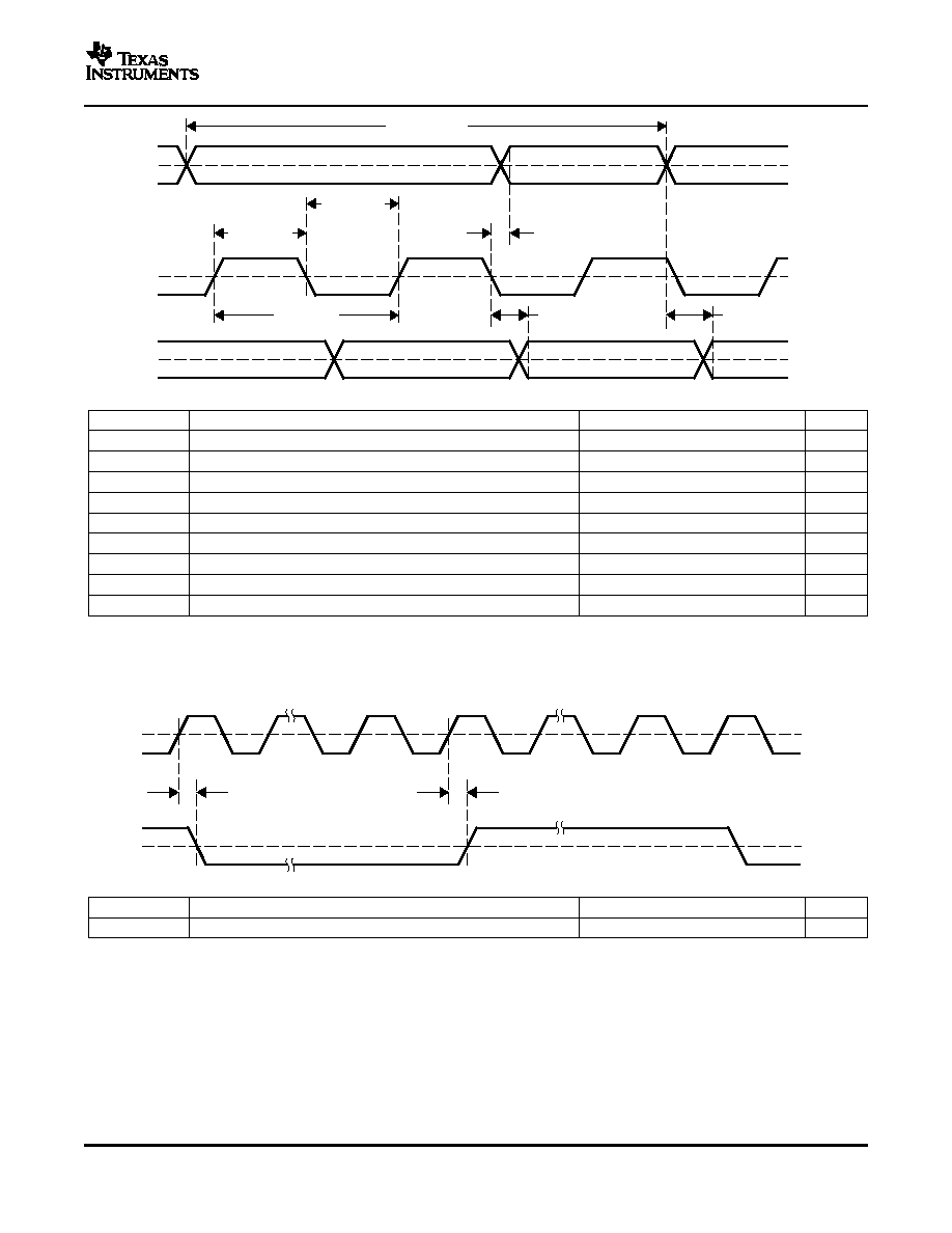
BCK
LRCK
DOUT
t
(BCKH)
t
(BCKL)
t
(CKLR)
t
(LRCP)
t
(BCKP)
t
(CKDO)
t
(LRDO)
0.5 V
DD
0.5 V
DD
0.5 V
DD
T0018-02
BCK
SCKI
t
(SCKBCK)
1.4 V
0.5 V
DD
T0074-01
t
(SCKBCK)
PCM1803A
SLES142A ≠ JUNE 2005 ≠ REVISED AUGUST 2006
SYMBOL
PARAMETER
MIN
TYP
MAX
UNIT
t
(BCKP)
BCK period
150
1/(64 f
S
)
1000
ns
t
(BCKH)
BCK pulse duration, HIGH
65
600
ns
t
(BCKL)
BCK pulse duration, LOW
65
600
ns
t
(CKLR)
Delay time, BCK falling edge to LRCK valid
≠10
20
ns
t
(LRCP)
LRCK period
10
1/f
S
65
µ
s
t
(CKDO)
Delay time, BCK falling edge to DOUT valid
≠10
20
ns
t
(LRDO)
Delay time, LRCK edge to DOUT valid
≠10
20
ns
t
r
Rising time of all signals
20
ns
t
f
Falling time of all signals
20
ns
NOTE: Timing measurement reference level is 1.4 V for input and 0.5 V
DD
for output. Rising and falling time is measured
from 10% to 90% of IN/OUT signal swing. Load capacitance of all signals is 20 pF.
Figure 21. Audio Data Interface Timing (Master Mode: LRCK and BCK Work as Outputs)
SYMBOL
PARAMETER
MIN
TYP
MAX
UNIT
t
(SCKBCK)
Delay time, SCKI rising edge to BCK edge
5
30
ns
NOTE: Timing measurement reference level is 1.4 V for input and 0.5 V
DD
for output. Load capacitance of BCK is 20 pF.
Figure 22. Audio Clock Interface Timing (Master Mode: BCK Works as Output)
15
Submit Documentation Feedback
www.ti.com
SYNCHRONIZATION WITH DIGITAL AUDIO SYSTEM
1/f
S
32/f
S
NORMAL DATA
ZERO DATA
UNDEFINED
DATA
NORMAL DATA
SYNCHRONOUS
ASYNCHRONOUS
SYNCHRONOUS
Resynchronization
Synchronization Lost
DOUT
State of Synchronization
T0020-05
PCM1803A
SLES142A ≠ JUNE 2005 ≠ REVISED AUGUST 2006
In slave mode, the PCM1803A operates under LRCK, synchronized with system clock SCKI. The PCM1803A
does not need a specific phase relationship between LRCK and SCKI, but does require the synchronization of
LRCK and SCKI.
If the relationship between LRCK and SCKI changes more than
±
6 BCKs for 64 BCK/frame (
±
5 BCKs for 48
BCK/frame) during one sample period due to LRCK or SCKI jitter, internal operation of the ADC halts within 1/f
S
,
and digital output is forced to zero data (BPZ code) until resynchronization between LRCK and SCKI occurs.
In case of changes less than
±
5 BCKs for 64 BCK/frame (
±
4 BCKs for 48 BCK/frame), resynchronization does
not occur and the previously explained digital output control and discontinuity do not occur.
Figure 23
illustrates the digital output response for loss of synchronization and resynchronization. During
undefined data, the PCM1803A can generate some noise in the audio signal. Also, the transition of normal to
undefined data and undefined or zero data to normal creates a discontinuity in the data of the digital output,
which can generate some noise in the audio signal.
Figure 23. ADC Digital Output for Loss of Synchronization and Resynchronization
16
Submit Documentation Feedback
www.ti.com
POWER DOWN
HPF BYPASS
OVERSAMPLING RATIO CONTROL
PCM1803A
SLES142A ≠ JUNE 2005 ≠ REVISED AUGUST 2006
PDWN (pin 7) controls operation of the entire ADC. During power-down mode, supply current for the analog
portion is shut down and the digital portion is reset; also, DOUT (pin 12) is disabled. It is acceptable to halt the
system clock during power-down mode so that power dissipation is minimized. The minimum LOW pulse
duration on the PDWN pin is 100 ns.
It is recommended to set PWDN (pin 7) to LOW once to obtain stable analog performance when the sampling
rate, interface mode, data format, or oversampling control is changed.
Table 4. Power-Down Control
PWDN
Power-Down Mode
LOW
Power-down mode
HIGH
Normal operation mode
The built-in function for dc-component rejection can be bypassed by BYPAS (pin 8) control. In bypass mode, the
dc component of the input analog signal, internal dc offset, etc., also are converted and included in the digital
output data.
Table 5. HPF Bypass Control
BYPAS
HPF (High-Pass Filter) Mode
LOW
Normal (no dc component in DOUT) mode
HIGH
Bypass (dc component in DOUT) mode
OSR (pin 16) controls the oversampling ratio of the delta-sigma modulator, ◊64 or ◊128. The ◊128 mode is
available for f
S
48 kHz.
Table 6. Oversampling Control
OSR
Oversampling Ratio
LOW
◊64
HIGH
◊128 (f
S
48 kHz)
17
Submit Documentation Feedback
www.ti.com
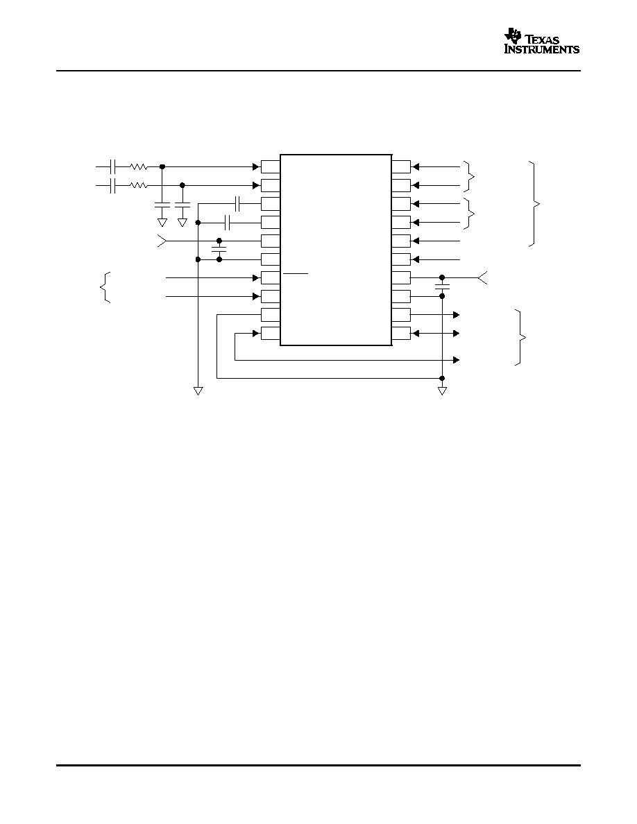
APPLICATION INFORMATION
TYPICAL CIRCUIT CONNECTION DIAGRAM
V
IN
L
20
19
18
17
16
15
14
13
12
11
1
2
3
4
5
6
7
8
9
10
PCM1803A
V
IN
R
V
REF
1
V
REF
2
V
CC
AGND
PDWN
BYPAS
TEST
LRCK
MODE1
DGND
MODE0
FMT1
FMT0
OSR
DOUT
BCK
V
DD
SCKI
+
Oversampling
System Clock
L-Ch IN
R-Ch IN
+5 V
C
4
+
C
5
Power Down
LCF Bypass
Control
+
C
3
L/R Clock
Audio Data
Processor
Mode [1:0]
Format [1:0]
+3.3 V
Data Clock
Data Out
+
C
1
+
C
2
Control
R
1
S0026-03
+
C
6
R
2
C
7
C
8
PCM1803A
SLES142A ≠ JUNE 2005 ≠ REVISED AUGUST 2006
Figure 24
illustrates a typical circuit connection diagram where the cutoff frequency of the input HPF is about
160 kHz.
NOTES:
A.
C
1
, C
2
: A 1-
µ
F electrolytic capacitor gives a 4-Hz (
= 1
µ
F ◊ 40 k
) cutoff frequency for the input HPF in normal
operation and requires a power-on settling time with a 40-ms time constant during the power-on initialization period.
B.
C
3
, C
4
: Bypass capacitors are 0.1-
µ
F ceramic and 10-
µ
F electrolytic, depending on layout and power supply.
C.
C
5
, C
6
: Recommended capacitors are 0.1-
µ
F ceramic and 10-
µ
F electrolytic.
D.
C
7
, C
8
, R
1
, R
2
: A 0.01-
µ
F film-type capacitor and 100-
resistor give a 160-kHz (
= 0.01
µ
F ◊ 100
) cutoff
frequency for the anti-aliasing filter in normal operation.
Figure 24. Typical Application Diagram
18
Submit Documentation Feedback

www.ti.com
BOARD DESIGN and LAYOUT CONSIDERATIONS
V
CC
, V
DD
Pins
AGND, DGND Pins
V
IN
L, V
IN
R Pins
V
REF
1 Pin
V
REF
2 Pin
DOUT Pin
System Clock
PCM1803A
SLES142A ≠ JUNE 2005 ≠ REVISED AUGUST 2006
APPLICATION INFORMATION (continued)
The digital and analog power-supply lines to the PCM1803A should be bypassed to the corresponding ground
pins with 0.1-
µ
F ceramic and 10-
µ
F electrolytic capacitors, as close to the pins as possible, to maximize the
dynamic performance of the ADC.
To maximize the dynamic performance of the PCM1803A, the analog and digital grounds are not connected
internally. These grounds should have low impedance to avoid digital noise feeding back into the analog ground.
Therefore, they should be connected directly to each other under the part to reduce potential noise problems.
The V
IN
L and V
IN
R pins need a simple external RC filter (f
C
= 160 kHz) as an antialiasing filter to remove
out-of-band noise from the audio band. If the input signal includes noise with a frequency near the oversampling
frequency (64 f
S
or 128 f
S
), the noise is folded into the baseband (audio band) signal through A-to-D conversion.
The recommended R value is 100
. Film-type capacitors of 0.01-
µ
F should be located as close as possible to
the V
IN
L and V
IN
R pins and should be terminated to GND as close as possible to the AGND pin to maximize the
dynamic performance of ADC, by suppressing kickback noise from the PCM1803A.
A 0.1-
µ
F ceramic capacitor and 10-
µ
F electrolytic capacitor are recommended between V
REF
1 and AGND to
ensure low source impedance of the ADC references. These capacitors should be located as close as possible
to the V
REF
1 pin to reduce dynamic errors on the ADC reference.
The differential voltage between V
REF
2 and AGND sets the analog input full-scale range. A 0.1-
µ
F ceramic
capacitor and 10-
µ
F electrolytic capacitor are recommended between V
REF
2 and AGND. These capacitors
should be located as close as possible to the V
REF
2 pin to reduce dynamic errors on the ADC reference.
The DOUT pin has enough load drive capability, but if the DOUT line is long, locating a buffer near the
PCM1803A and minimizing load capacitance is recommended to minimize the digital-analog crosstalk and
maximize the dynamic performance of the ADC.
The quality of the system clock can influence the dynamic performance, because the PCM1803A operates
based on a system clock. Therefore, it may be required to consider the system-clock duty, jitter, and the time
difference between system-clock transition and BCK or LRCK transition in the slave mode.
19
Submit Documentation Feedback

PACKAGING INFORMATION
Orderable Device
Status
(1)
Package
Type
Package
Drawing
Pins Package
Qty
Eco Plan
(2)
Lead/Ball Finish
MSL Peak Temp
(3)
PCM1803ADB
ACTIVE
SSOP
DB
20
65
Green (RoHS &
no Sb/Br)
CU NIPDAU
Level-1-260C-UNLIM
PCM1803ADBG4
ACTIVE
SSOP
DB
20
65
Green (RoHS &
no Sb/Br)
CU NIPDAU
Level-1-260C-UNLIM
PCM1803ADBR
ACTIVE
SSOP
DB
20
2000 Green (RoHS &
no Sb/Br)
CU NIPDAU
Level-1-260C-UNLIM
PCM1803ADBRG4
ACTIVE
SSOP
DB
20
2000 Green (RoHS &
no Sb/Br)
CU NIPDAU
Level-1-260C-UNLIM
(1)
The marketing status values are defined as follows:
ACTIVE: Product device recommended for new designs.
LIFEBUY: TI has announced that the device will be discontinued, and a lifetime-buy period is in effect.
NRND: Not recommended for new designs. Device is in production to support existing customers, but TI does not recommend using this part in
a new design.
PREVIEW: Device has been announced but is not in production. Samples may or may not be available.
OBSOLETE: TI has discontinued the production of the device.
(2)
Eco Plan - The planned eco-friendly classification: Pb-Free (RoHS), Pb-Free (RoHS Exempt), or Green (RoHS & no Sb/Br) - please check
http://www.ti.com/productcontent
for the latest availability information and additional product content details.
TBD: The Pb-Free/Green conversion plan has not been defined.
Pb-Free (RoHS): TI's terms "Lead-Free" or "Pb-Free" mean semiconductor products that are compatible with the current RoHS requirements
for all 6 substances, including the requirement that lead not exceed 0.1% by weight in homogeneous materials. Where designed to be soldered
at high temperatures, TI Pb-Free products are suitable for use in specified lead-free processes.
Pb-Free (RoHS Exempt): This component has a RoHS exemption for either 1) lead-based flip-chip solder bumps used between the die and
package, or 2) lead-based die adhesive used between the die and leadframe. The component is otherwise considered Pb-Free (RoHS
compatible) as defined above.
Green (RoHS & no Sb/Br): TI defines "Green" to mean Pb-Free (RoHS compatible), and free of Bromine (Br) and Antimony (Sb) based flame
retardants (Br or Sb do not exceed 0.1% by weight in homogeneous material)
(3)
MSL, Peak Temp. -- The Moisture Sensitivity Level rating according to the JEDEC industry standard classifications, and peak solder
temperature.
Important Information and Disclaimer:The information provided on this page represents TI's knowledge and belief as of the date that it is
provided. TI bases its knowledge and belief on information provided by third parties, and makes no representation or warranty as to the
accuracy of such information. Efforts are underway to better integrate information from third parties. TI has taken and continues to take
reasonable steps to provide representative and accurate information but may not have conducted destructive testing or chemical analysis on
incoming materials and chemicals. TI and TI suppliers consider certain information to be proprietary, and thus CAS numbers and other limited
information may not be available for release.
In no event shall TI's liability arising out of such information exceed the total purchase price of the TI part(s) at issue in this document sold by TI
to Customer on an annual basis.
PACKAGE OPTION ADDENDUM
www.ti.com
5-Jul-2006
Addendum-Page 1
MECHANICAL DATA
MSSO002E ≠ JANUARY 1995 ≠ REVISED DECEMBER 2001
POST OFFICE BOX 655303
∑
DALLAS, TEXAS 75265
DB (R-PDSO-G**)
PLASTIC SMALL-OUTLINE
4040065 /E 12/01
28 PINS SHOWN
Gage Plane
8,20
7,40
0,55
0,95
0,25
38
12,90
12,30
28
10,50
24
8,50
Seating Plane
9,90
7,90
30
10,50
9,90
0,38
5,60
5,00
15
0,22
14
A
28
1
20
16
6,50
6,50
14
0,05 MIN
5,90
5,90
DIM
A MAX
A MIN
PINS **
2,00 MAX
6,90
7,50
0,65
M
0,15
0
∞
≠ 8
∞
0,10
0,09
0,25
NOTES: A. All linear dimensions are in millimeters.
B. This drawing is subject to change without notice.
C. Body dimensions do not include mold flash or protrusion not to exceed 0,15.
D. Falls within JEDEC MO-150

IMPORTANT NOTICE
Texas Instruments Incorporated and its subsidiaries (TI) reserve the right to make corrections, modifications,
enhancements, improvements, and other changes to its products and services at any time and to discontinue
any product or service without notice. Customers should obtain the latest relevant information before placing
orders and should verify that such information is current and complete. All products are sold subject to TI's terms
and conditions of sale supplied at the time of order acknowledgment.
TI warrants performance of its hardware products to the specifications applicable at the time of sale in
accordance with TI's standard warranty. Testing and other quality control techniques are used to the extent TI
deems necessary to support this warranty. Except where mandated by government requirements, testing of all
parameters of each product is not necessarily performed.
TI assumes no liability for applications assistance or customer product design. Customers are responsible for
their products and applications using TI components. To minimize the risks associated with customer products
and applications, customers should provide adequate design and operating safeguards.
TI does not warrant or represent that any license, either express or implied, is granted under any TI patent right,
copyright, mask work right, or other TI intellectual property right relating to any combination, machine, or process
in which TI products or services are used. Information published by TI regarding third-party products or services
does not constitute a license from TI to use such products or services or a warranty or endorsement thereof.
Use of such information may require a license from a third party under the patents or other intellectual property
of the third party, or a license from TI under the patents or other intellectual property of TI.
Reproduction of information in TI data books or data sheets is permissible only if reproduction is without
alteration and is accompanied by all associated warranties, conditions, limitations, and notices. Reproduction
of this information with alteration is an unfair and deceptive business practice. TI is not responsible or liable for
such altered documentation.
Resale of TI products or services with statements different from or beyond the parameters stated by TI for that
product or service voids all express and any implied warranties for the associated TI product or service and
is an unfair and deceptive business practice. TI is not responsible or liable for any such statements.
Following are URLs where you can obtain information on other Texas Instruments products and application
solutions:
Products
Applications
Amplifiers
amplifier.ti.com
Audio
www.ti.com/audio
Data Converters
dataconverter.ti.com
Automotive
www.ti.com/automotive
DSP
dsp.ti.com
Broadband
www.ti.com/broadband
Interface
interface.ti.com
Digital Control
www.ti.com/digitalcontrol
Logic
logic.ti.com
Military
www.ti.com/military
Power Mgmt
power.ti.com
Optical Networking
www.ti.com/opticalnetwork
Microcontrollers
microcontroller.ti.com
Security
www.ti.com/security
Low Power Wireless www.ti.com/lpw
Telephony
www.ti.com/telephony
Video & Imaging
www.ti.com/video
Wireless
www.ti.com/wireless
Mailing Address:
Texas Instruments
Post Office Box 655303 Dallas, Texas 75265
Copyright
2006, Texas Instruments Incorporated