1
Æ
PCM2702
Æ
PCM2702
16-Bit Stereo
DIGITAL-TO-ANALOG CONVERTER
with Interface
FEATURES
q
INTEGRATED USB INTERFACE:
Full-Speed Transceiver Supports 12Mbps
Data Transfer.
Fully Compliant with the USB 1.0 Specifi-
cation.
Adaptive Mode for Isochronous Transfer.
Self-Powered Device.
q
ACCEPTS 16-BIT STEREO AND MONO
USB AUDIO DATA STREAMS.
q
ANALOG PERFORMANCE (V
CC
= 5V):
Dynamic Range: 100dB (typ at 16-bit)
SNR: 105dB (typ)
THD+N: 0.002% (typ at 16-bit)
Full-Scale Output: 3.1Vp-p
q
8X OVERSAMPLING DIGITAL FILTER:
Passband: 0.454f
S
Stopband: 0.546f
S
Passband Ripple:
±
0.002dB
Stopband Attenuation: ≠82dB
q
SAMPLING RATE (F
S
): 32kHz, 44.1kHz,
48kHz
q
ON-CHIP CLOCK GENERATOR
WITH SINGLE 12MHz CLOCK SOURCE
q
MULTI-FUNCTIONS:
Digital Attenuator: 0dB to ≠64dB, 1dB/step
Soft Mute
Zero Flag
Suspend Flag
Playback Flag
q
DUAL POWER SUPPLIES:
+5V for Analog portion
+3.3V for Digital portion
q
PACKAGE: SSOP-28
DESCRIPTION
The PCM2702 is a single chip digital-to-analog con-
verter offering two D/A output channels and an inte-
grated USB 1.0 compliant interface controller. The
newly developed SpActTM (Sampling Period Adaptive
Controlled Tracking) system recovers a stable, low-
jitter clock for internal PLL and DAC operation from
the USB interface audio data.
The PCM2702 is based upon Burr-Brown's Enhanced
Multi-level Delta-Sigma Modulator, an 8x
oversampling digital interpolation filter, and an analog
output low-pass filter.
The PCM2702 can accept a 48kHz, 44.1kHz and
32kHz sampling rates, using either 16-bit stereo or
monaural audio data. Digital attenuation and soft-
mute features are included, and are controlled via USB
audio class request.
Patents Pending.
SpActTM is a trademark of Burr-Brown Corporation.
©
2000 Burr-Brown Corporation
PDS-1584A
Printed in U.S.A. May, 2000
International Airport Industrial Park ∑ Mailing Address: PO Box 11400, Tucson, AZ 85734 ∑ Street Address: 6730 S. Tucson Blvd., Tucson, AZ 85706 ∑ Tel: (520) 746-1111
Twx: 910-952-1111 ∑ Internet: http://www.burr-brown.com/ ∑ Cable: BBRCORP ∑ Telex: 066-6491 ∑ FAX: (520) 889-1510 ∑ Immediate Product Info: (800) 548-6132
For most current data sheet and other product
information, visit www.burr-brown.com
APPLICATIONS
q
STAND-ALONE USB AUDIO SPEAKERS
q
CRT/LCD INTEGRATED USB AUDIO SPEAKERS
q
USB AUDIO AMPLIFIERS
q
OTHER USB AUDIO APPLICATIONS
PCM2702
SBAS142

2
Æ
PCM2702
SPECIFICATIONS
At T
A
= +25
∞
C, V
CC
= V
CC
L = V
CC
R = V
CC
P = 5.0V, V
DD
= V
DD
C = 3.3V, f
S
= 44.1MHz, signal frequency = 1kHz and 16-bit data, unless otherwise specified.
PCM2702E
PARAMETER
CONDITIONS
MIN
TYP
MAX
UNITS
RESOLUTION
16
Bits
HOST INTERFACE
Supports USB revision 1.0, Full Speed
DIGITAL FORMAT
Audio Data Format
USB ISOCHRONOUS OUT
Audio Data Bit Length
16
Audio Data Channel
1, 2
Sampling Frequency (f
S
)
32, 44.1, 48
DIGITAL INPUT/OUTPUT
Input Logic Level
V
IH
(1)
2.0
VDC
V
IL
(1)
0.8
VDC
V
IH
(2)
0.7 V
DD
VDC
V
IL
(2)
0.7 V
DD
VDC
Input Logic Current
I
IH
(1)
V
IN
= V
DD
+65
+100
µ
A
I
IL
(1)
V
IN
= 0V
±
10
µ
A
I
IH
(2)
V
IN
= V
DD
±
10
µ
A
I
IL
(2)
V
IN
= 0V
±
10
µ
A
Output Logic Level
V
OH
(3)
I
OH
= ≠1mA
2.8
VDC
V
OL
(3)
I
OL
= +1mA
0.5
VDC
DYNAMIC PERFORMANCE
(4)
THD+N at V
OUT
= 0dB
0.002
0.005
%
THD+N at V
OUT
= ≠60dB
1.2
%
Dynamic Range
EIAJ, A-Weighted
96
100
dB
SIgnal-to-Noise Ratio
EIAJ, A-Weighted
100
105
dB
Channel Seperation
98
103
dB
DC ACCURACY
Gain Error
±
1.0
±
3.0
% of FSR
Gain Mismatch, Channel-to-Channel
±
1.0
±
3.0
% of FSR
Bipolar Zero Error
V
OUT
= 0.5 V
CC
at BPZ
±
30
±
60
mV
ANALOG OUTPUT
Output Voltage
Full-Scale(≠0dB)
62% of V
CC
Vp-p
Center Voltage
50% of V
CC
VDC
Load Impedance
AC-Load
5
k
DIGITAL FILTER PERFORMANCE
Passband
±
0.002dB
0.454f
S
Passband
≠3dB
0.490f
S
Stopband
0.546f
S
Passband Ripple
±
0.002
dB
Stopband Attenuation
Stopband = 0.546f
S
≠75
dB
Stopband Attenuation
Stopband = 0.567f
S
≠82
dB
Delay Time
34/f
S
11
s
ANALOG FILTER PERFORMANCE
Frequency Response
at 20kHz
0.02
dB
POWER SUPPLY REQUIREMENTS
Voltage Range
V
DD
, V
DD
C
+3.0
+3.3
+3.6
VDC
V
CC
, V
CC
L, V
CC
R, V
CC
P
+4.5
+5.0
+5.5
VDC
Supply Current
I
DD
V
DD
= V
DD
C = 3.3V
22
30
mA
I
CC
V
CC
= V
CC
L = V
CC
R = V
CC
P = 5.0V
18
25
mA
Power Dissipation
V
DD
= V
DD
C = 3.3V, and V
CC
= V
CC
L = V
CC
R = V
CC
P = 5.0V
165
225
mW
TEMPERATURE RANGE
Operation Temperature
0
70
∞
C
Storage Temperature
≠55
+125
∞
C
Thermal Resistance,
JA
SSOP-28
100
∞
C/W
NOTES: (1) Pins 8, 13, 14, 15, 16: V
BUS
, TEST3 TEST2 TEST1, TEST0. (2) Pin1: XTI. (3) Pins 10, 11, 12, 28: PLYBCK, SSPND, ZERO, XTO. (4) The dynamic
performance is based upon ideal host signal quality, and may vary according to the system. Dynamic performance specifications are tested using a Shibasoku #725
THD Meter with 400Hz HPF, 30kHz LPF, Average Mode, and 20kHz Bandwidth limiting. The load connected to the analog output is 5k
, or larger, via AC coupling.
The information provided herein is believed to be reliable; however, BURR-BROWN assumes no responsibility for inaccuracies or omissions. BURR-BROWN
assumes no responsibility for the use of this information, and all use of such information shall be entirely at the user's own risk. Prices and specifications are subject
to change without notice. No patent rights or licenses to any of the circuits described herein are implied or granted to any third party. BURR-BROWN does not
authorize or warrant any BURR-BROWN product for use in life support devices and/or systems.
3
Æ
PCM2702
Supply Voltage
(2) ..............................................................................................................
+6.5V
Supply Voltage
(3) ..............................................................................................................
+4.0V
Supply Voltage Differences
(4) ..................................................................................
±
0.1V
Supply Voltage Differences
(5) ..................................................................................
±
0.1V
Ground Voltage Differences
(6) .................................................................................
±
0.1V
Digital Input Voltage
(7) .................................................................
≠0.3V to V
DD
+ 0.3V
Digital Input Voltage
(8) ................................................................................
≠0.3V to 6.5V
Analog Input Voltage ................................................ ≠0.3V to V
CC
+ 0.3V
Input Current (any pins except supplies) .......................................
±
10mA
Operating Temperature .................................................. ≠25
∞
C to +85
∞
C
Storage Temperature ..................................................... ≠55
∞
C to +125
∞
C
Junction Temperature .................................................................... +150
∞
C
Lead Temperature (soldering, 5s) ................................................. +260
∞
C
Package Temperature (IR reflow, peak, 10s) ............................... +235
∞
C
NOTES: (1) Stresses above those listed under Absolute Maximum Ratings
may cause permanent damage to the device. Exposure to absolute maximum
conditions for extended periods may affect device reliability.
(2) V
CC
, V
CC
L, V
CC
R, V
DD
P. (3) V
DD
, V
DD
C. (4) Among V
CC
, V
CC
L, V
CC
R, V
CC
P.
(5) Among V
DD
, V
DD
C. (6) Among AGND, AGNDL, AGNDR, AGNDP, DGND,
DGNDC, and DGNDU. (7) XTI, D+, D≠, PLYBCK, SSPND, ZERO, XTO.
(8) V
BUS
, TEST#, TEST2, TEST1, TEST0.
ABSOLUTE MAXIMUM RATINGS
(1)
ELECTROSTATIC
DISCHARGE SENSITIVITY
This integrated circuit can be damaged by ESD. Burr-Brown
recommends that all integrated circuits be handled with
appropriate precautions. Failure to observe proper handling
and installation procedures can cause damage.
ESD damage can range from subtle performance degrada-
tion to complete device failure. Precision integrated circuits
may be more susceptible to damage because very small
parametric changes could cause the device not to meet its
published specifications.
PACKAGE
SPECIFIED
DRAWING
TEMPERATURE
PACKAGE
ORDERING
TRANSPORT
PRODUCT
PACKAGE
NUMBER
RANGE
MARKING
NUMBER
(1)
MEDIA
PCM2702E
SSOP-28
324
0
∞
C to +70
∞
C
PCM2702E
PCM2702E
Rails
"
"
"
"
"
PCM2702E/2K
Tape and Reel
NOTE: (1) Models with a slash (/) are available only in Tape and Reel in the quantities indicated (e.g., /2K indicates 2000 devices per reel). Ordering 2000 pieces
of "PCM2702E/2K" will get a single 2000-piece Tape and Reel.
PACKAGE/ORDERING INFORMATION
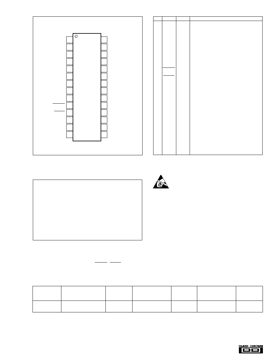
PIN
NAME
TYPE
DESCRIPTIONS
1
XTI
IN
Crystal Oscillator Input.
(1)
2
V
DD
C
--
Digital Power Supply for Clock Generator,
+3.3V.
3
DGNDC
--
Digital Ground for Clock Generator.
4
V
DD
--
Digital Power Supply, +3.3V.
5
DGND
--
Digital Ground.
6
D+
IN/OUT
USB Differential Input/Output Plus.
7
D≠
IN/OUT
USB Differential Input/Output Minus.
8
V
BUS
IN
USB Bus Power (this pin NEVER consumes
USB bus power).
(2)
9
DGNDU
--
Digital Ground for USB Transceiver.
10 PLYBCK
OUT
Playback flag, active LOW (LOW: playback,
HIGH: idle).
11
SSPND
OUT
Suspend flag, active LOW (LOW: suspend,
HIGH: operational).
12
ZERO
OUT
Zero flag (LOW: Normal, HIGH: ZERO.)
13
TEST3
IN
Test pin 3. Connect to digital ground.
(2)
14
TEST2
IN
Test pin 2. Connect to digital ground.
(2)
15
TEST1
IN
Test pin 1. Connect to digital ground.
(2)
16
TEST0
IN
Test pin 0. Connect to digital ground.
(2)
17
V
CC
R
--
Analog Supply for R-channel, +5V.
18
AGNDR
--
Analog Ground for R-channel.
19
V
OUT
R
OUT
Analog Output for R-channel.
20
AGND
--
Analog Ground.
21
V
COM
--
DC Common-Mode Voltage for DAC.
22
V
CC
--
Analog Supply, +5V.
23
V
OUT
L
OUT
Analog Output for L-channel.
24
AGNDL
--
Analog Ground for L-channel.
25
V
CC
L
--
Analog Supply for L-channel, +5V.
26
AGNDP
--
Analog Ground for PLL.
27
V
CC
P
--
Analog Supply for PLL, +5V.
28
XTO
OUT
Crystal Oscillator Output.
NOTES: (1) 3.3 V tolerant. (2) Schmitt trigger input with internal pull-down,
5V tolerant.
XTI
V
DD
C
DGNDC
V
DD
DGND
D+
D≠
V
BUS
DGNDU
PLYBCK
SSPND
ZERO
TEST3
TEST2
XTO
V
CC
P
AGNDP
V
CC
L
AGNDL
V
OUT
L
V
CC
V
COM
AGND
V
OUT
R
AGNDR
V
CC
R
TEST0
TEST1
1
2
3
4
5
6
7
8
9
10
11
12
13
14
28
27
26
25
24
23
22
21
20
19
18
17
16
15
PCM2702
Top View
SSOP
4
Æ
PCM2702
BLOCK DIAGRAM
DAC
DAC
SpActTM
Audio
Clock
Generator
8x
Oversampling
Digital Filter
Multi-
Level
Delta-
Sigma
Modulator
USB
I/F
Low-Pass
Filter
Low-Pass
Filter
Power Supply
Crystal
OSC
FIFO
mclk
System Clock
wrclk
USB
Packet
Data
Audio
Data
V
OUT
L
V
COM
V
OUT
R
rdclk
USB
Clock
Generator
PLYBCK
V
DD
P
DGNDP
XTI
XTO
V
CC
AGND
V
DD
DGND
D+
D≠
V
BUS
V
DD
C
DGNDU
DGNDC
SSPND
ZERO
V
CC
L
AGNDL
V
CC
R
AGNDR
5
Æ
PCM2702
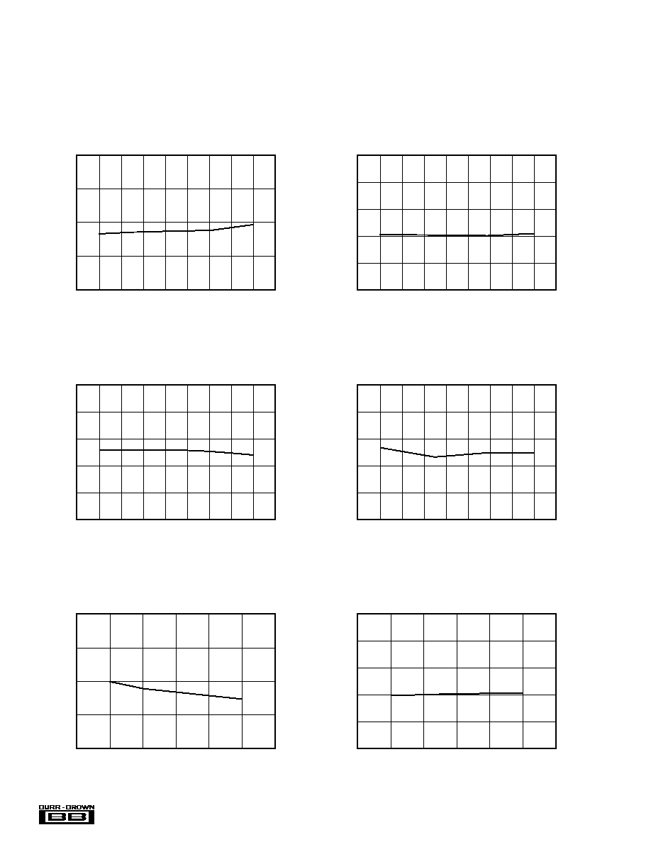
TYPICAL PERFORMANCE CURVES
All specifications at T
A
= +25
∞
C, V
CC
= V
CC
L = V
CC
R = V
CC
P = 5.0V, V
DD
= V
DD
C = 3.3V, f
S
= 44.1MHz, signal frequency = 1kHz and 16-bit data, unless
otherwise specified.
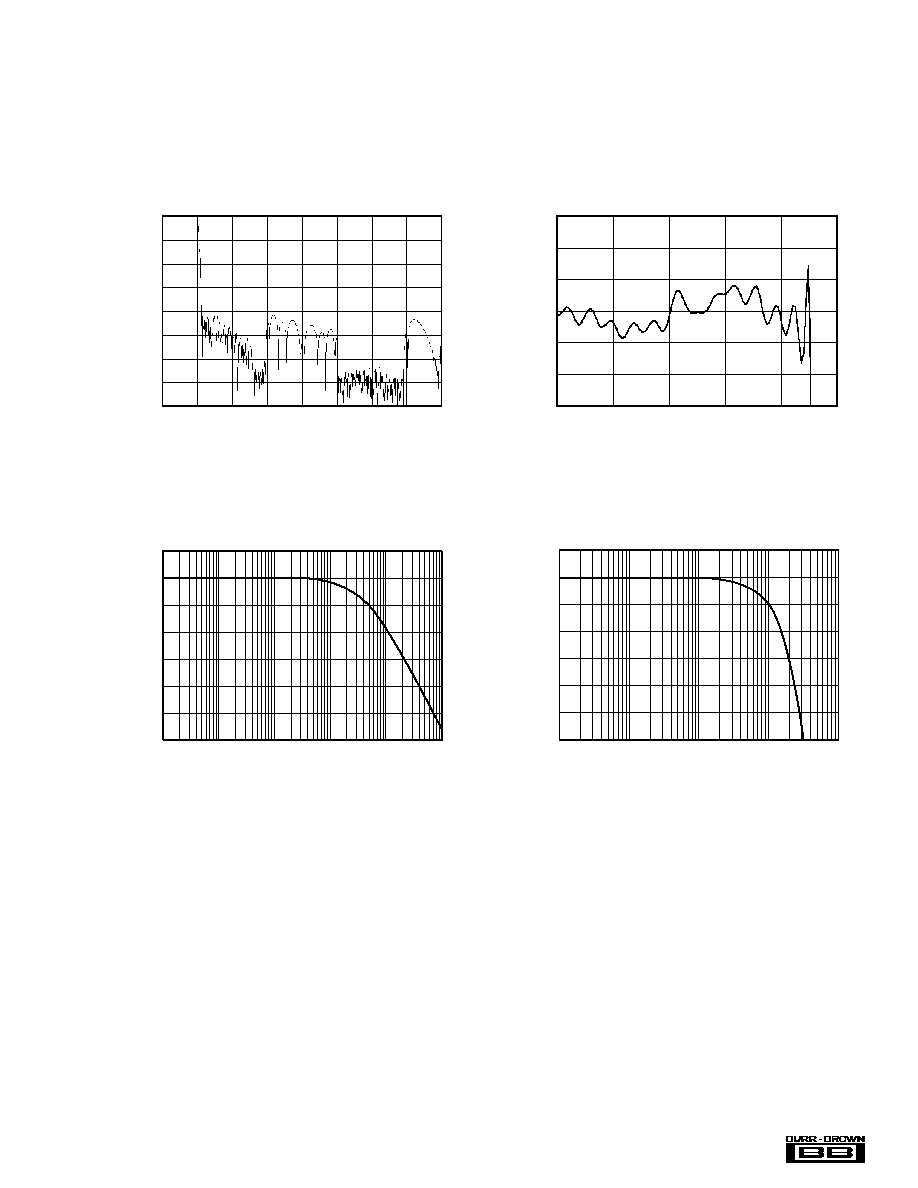
FREQUENCY RESPONSE
Frequency (x f
S
)
(dB)
1
1.5
2
2.5
3
3.5
4
0.5
0
0
≠20
≠40
≠60
≠80
≠100
≠120
≠140
≠160
PASSBAND RIPPLE
Frequency (x f
S
)
(dB)
0.2
0.3
0.4
0.5
0.1
0
0.003
0.002
0.001
0
≠0.001
≠0.002
≠0.003
ANALOG FILTER PERFORMANCE (100MHz-10Hz)
Frequency (Hz)
Response (dB)
10k
100k
1M
10M
1k
100
10
0
≠10
≠20
≠30
≠40
≠50
≠60
ANALOG FILTER PERFORMANCE (100MHz-1MHz)
Frequency (Hz)
Response (dB)
10k
100k
1M
1k
100
1
0
≠1
≠2
≠3
≠4
≠5
≠6
DIGITAL FILTER PERFORMANCE
ANALOG FILTER PERFORMANCE
6
Æ
PCM2702
TYPICAL PERFORMANCE CURVES (Cont.)
All specifications at T
A
= +25
∞
C, V
CC
= V
CC
L = V
CC
R = V
CC
P = 5.0V, V
DD
= V
DD
C = 3.3V, f
S
= 44.1MHz, signal frequency = 1kHz and 16-bit data, unless
otherwise specified.
THD+N (0dB) vs T
A
T
A
(
∞
C)
THD+N (0dB) (%)
50
40
30
20
70
60
80
10
0
≠10
0.003
0.002
0.001
DYNAMIC RANGE vs T
A
T
A
(
∞
C)
Dynamic Range (dB)
50
40
30
20
70
60
80
10
0
≠10
106
104
102
100
98
96
SOUND-TO-NOISE RATIO vs T
A
T
A
(
∞
C)
SNR (dB)
50
40
30
20
70
60
80
10
0
≠10
110
108
106
104
102
100
CHANNEL SEPARATION vs T
A
T
A
(
∞
C)
Channel Separation (dB)
50
40
30
20
70
60
80
10
0
≠10
108
106
104
102
100
98
THD+N (0dB) vs V
CC
V
CC
(V)
THD+N (0dB) (%)
5.0
4.75
5.5
5.25
5.75
4.5
4.25
0.003
0.002
0.001
DYNAMIC RANGE vs V
CC
V
CC
(V)
Dynamic Range (dB)
5.0
4.75
5.5
5.25
5.75
4.5
4.25
106
104
102
100
98
96
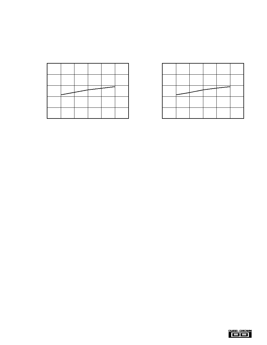
ANALOG DYNAMIC PERFORMANCE
7
Æ
PCM2702
TYPICAL PERFORMANCE CURVES (Cont.)
All specifications at T
A
= +25
∞
C, V
CC
= V
CC
L = V
CC
R = V
CC
P = 5.0V, V
DD
= V
DD
C = 3.3V, f
S
= 44.1MHz, signal frequency = 1kHz and 16-bit data, unless
otherwise specified.
CHANNEL SEPEARATION vs V
CC
V
CC
(V)
Channel Separation (dB)
5.0
4.75
5.5
5.25
5.75
4.5
4.25
108
106
104
102
100
98
SOUND-TO-NOISE RATIO vs V
CC
V
CC
(V)
SNR (dB)
5.0
4.75
5.5
5.25
5.75
4.5
4.25
110
108
106
104
102
100

8
Æ
PCM2702
THEORY OF OPERATION
USB INTERFACE
The description of the USB interface complies with Univer-
sal Serial Bus specification Rev. 1.0.
Control and audio data are both transferred to the PCM2702
via D+ (pin 6) and D≠ (pin 7). All data to/from the PCM2702
are transferred at full-speed. V
BUS
(pin 8) and DGNDU (pin
9) are also connected to the USB bus. V
BUS
(pin 8) never
consumes USB bus power, it is used only for detecting the
connection of the USB bus. The following information is
provided in the device descriptor.
The Input Terminal is defined as "USB stream" (terminal
type 0x0101). The Input Terminal can accept 2-channel
audio streams comprised of left and right channel data. The
Output Terminal is defined as a "speaker" (terminal type
0x0301). The Feature Unit supports the following sound
control features.
∑ Volume Control
∑ Mute Control
The built-in digital volume controller can be manipulated by
an audio class specific request from 0.0dB to ≠64.0dB in
steps of 1.0dB. Each channel can be set independently. The
master volume control is also supported. The built-in digital
mute controller can be manipulated by an audio class spe-
cific request. A master mute-control request is acceptable. A
request to an individual channel will be stalled and ignored.
Interface #1 has three alternative settings. Alternative setting
#0 is the Zero Bandwidth setting. Alternative setting #1 is
the 16-Bit Stereo setting, and is an operational setting.
Alternative setting #2 is the 16-Bit Monaural setting, and is
also an operational setting. The PCM2702 has the following
two endpoints.
∑ Control Endpoint (EP #0)
∑ Isochronous Audio Data Stream Endpoint (EP #2)
The Control Endpoint is a default endpoint and is used to
control all functions of the PCM2702 by the standard USB
request and the USB audio class specific request. The
Isochronous Audio Data Stream Endpoint is an audio sink
endpoint, which receives the PCM audio data, and accepts
the adaptive transfer mode.
USB Revision
1.0
Device Class
0x00 (device defined interface level)
Device Subclass
0x00 (not specified)
Device Protocol
0x00 (not specified)
Max Packet Size for Endpoint 0
8 byte
Vendor ID
0x08BB
Device ID
0x2702
Release
1.0
TABLE I. Device Definition.
DEVICE CONFIGURATION
Figure 1 illustrates USB audio function topology. The
PCM2702 has two interfaces. Each interface is constructed
by some alternative setting. Interface #0 has one alternative
setting. Alternative setting #0 describes the standard audio
control interface. The audio control interface is constructed
by a terminal. The PCM2702 has the following three termi-
nals.
∑ Input Terminal (IT)
∑ Output Terminal (OT)
∑ Feature Unit (FU)
Endpoint #0
PCM2702
Default
Endpoint
Endpoint #2
Audio Streaming Interface
(IF #1)
IT
TID1
OT
TID2
Standard Audio Control Interface (IF #0)
FU
UID3
Analog Out
NOTE: IT = Input Terminal (Terminal ID #1); OT = Output Terminal (Terminal ID #2); FU = Feature Unit (Unit ID #3).
FIGURE 1. USB Audio Function Topology.
9
Æ
PCM2702
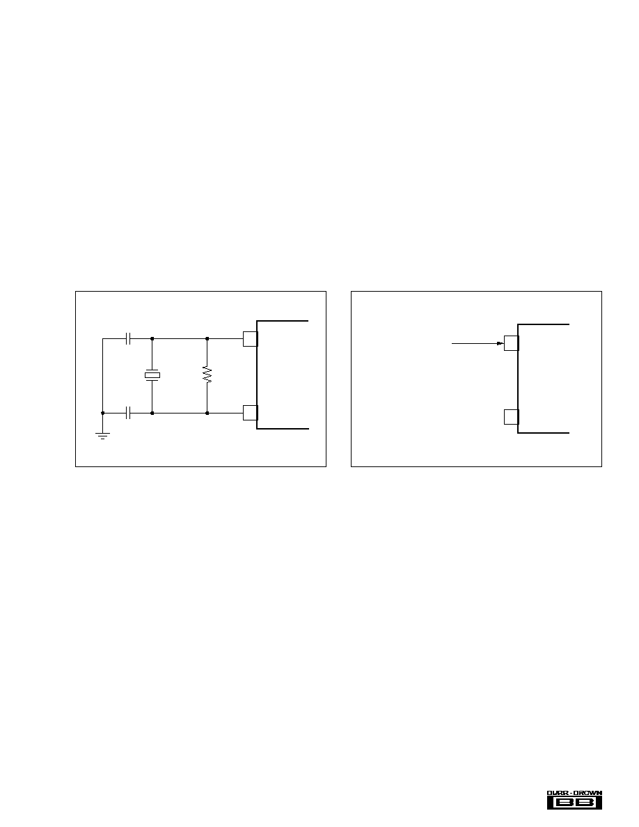
FIGURE 2. 12MHz Crystal Resonator Connection.
CLOCK AND RESET
The PCM2702 requires a 12MHz (
±
500ppm) clock for USB
and audio functions, which may be generated by an on-chip
crystal oscillator with external 12MHz crystal resonator, or
supplied by an external clock applied at XTI (pin1).
The 12MHz crystal resonator must be connected to XTI (pin
1) and XTO (pin 28), along with a 1M
resistor and two
small capacitors (value is dependent upon the specified load
capacitance of the crystal resonator). If an external clock is
used, the clock must be supplied at XTI, and XTO must be
left open. The clock signal applied at XTI must be +3.3V
logic level, as this input is not +5V tolerant. Figures 2 and
3 illustrate the circuit connections required for crystal and
external clock options.
The PCM2702 includes an internal power-on reset circuit,
which automatically initializes digital logic when V
DD
ex-
ceeds 2.0V typical (range: 1.6V to 2.4V). Initialization
requires approximately 350
µ
s for completion. The V
DD
supply must rise to 2.0V within 10ms for proper power-on
sequence operation.
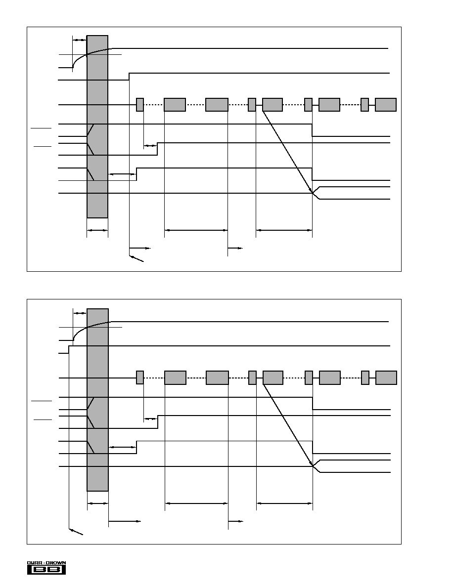
INTERFACE SEQUENCE
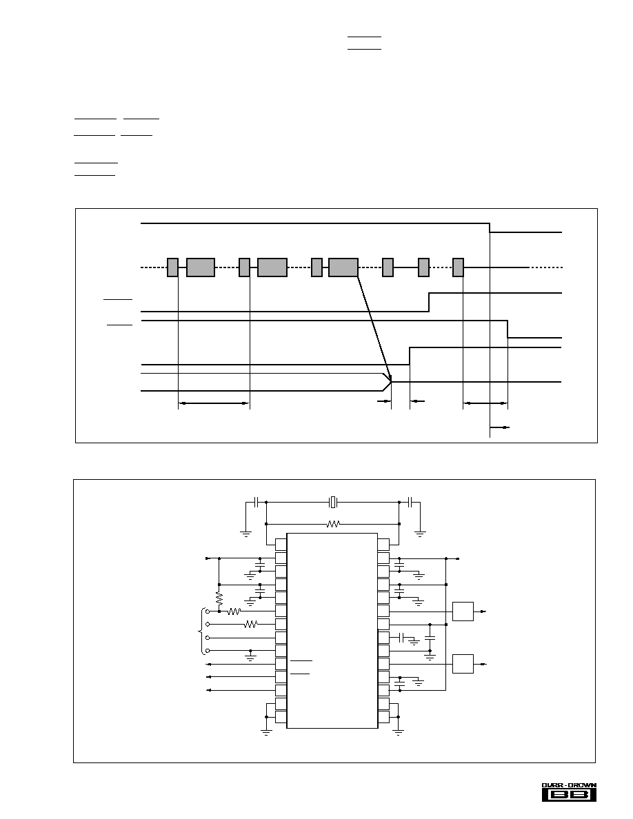
Power-on, Attach, and Playback Sequence
The PCM2702 is ready for setup when the reset sequence
has finished and the USB bus is connected. After connec-
tion is established, the PCM2702 is ready to accept USB
audio data. While waiting for audio data (idle state), the
analog outputs are set to bipolar zero (BPZ) and the zero
flag, ZERO (pin 12), is set to HIGH.
When receiving the audio data, the PCM2702 stores the first
audio packet, which contains 1ms of audio data, into an
internal storage buffer. The PCM2702 starts playing the
audio data upon detection of the Start of Frame (SOF)
packet.
See Figures 4 and 5 for the normal operation sequence.
FIGURE 3. External 12MHz Clock Input Connection.
1
28
XTAL
12MHz
1M
XTI
XTO
1
28
12MHz External Clock
Must Be Left Open
XTI
XTO
10
Æ
PCM2702
Ready for Setup
Ready for Playback
Attach (connect to USB bus)
Device Setup
1ms
23ms
(1024/f
S
)
1ms
10ms
SOF
SOF
SOF
SOF
2nd Audio Data
1st Audio Data
1st SOF
V
DD
0V
V
BUS
D+/D≠
PLYBCK
SSPND
ZERO
V
OUT
L
V
OUT
R
2.0V (1.6 to 2.4V)
350
µ
s
Internal
Reset
Ready for Setup
Ready for Playback
Device Setup
1ms
23ms
(1024/f
S
)
1ms
SOF
SOF
SOF
SOF
2nd Audio Data
1st Audio Data
1st SOF
V
DD
0V
V
BUS
D+/D≠
PLYBCK
SSPND
ZERO
V
OUT
L
V
OUT
R
2.0V (1.6 to 2.4V)
350
µ
s
Internal
Reset
Attach (connect to USB bus)
10ms
FIGURE 4. Connecting the PCM2702 to the USB Bus After Power-On.
FIGURE 5. Connecting the PCM2702 to the USB Bus Prior to Power-On.
11
Æ
PCM2702
Play, Stop, and Detach sequence
When host finishes or aborts audio playback, the PCM2702
will stop playing after the last transmitted audio data has
been received. Figure 6 shows the operation sequence for
play, stop, and detach.
PLYBCK, SSPND, AND ZERO FLAG
PLYBCK, SSPND, and Zero flag in Figures 4, 5, and 6 are
defined as follows.
PLYBCK--while PCM audio input data is playing back,
PLYBCK (pin 10) is switched LOW.
Detach
1ms
4ms
23ms
(1024/f
S
)
SOF
SOF
SOF
SOF
SOF
SOF
Audio Data
Last Audio Data
Audio Data
V
BUS
D+/D≠
PLYBCK
SSPND
ZERO
V
OUT
L
V
OUT
R
FIGURE 6. Play, Stop, and Detach.
SSPND--upon detection of a suspend state on the USB port,
SSPND (pin 11) is switched LOW.
ZERO--if the PCM audio input data is continuously zero
for 1024 sampling periods (1/f
S
), ZERO (pin12) is switched
to HIGH.
TEST PINS
The PCM2702 has four test pins--TEST0 (pin 16), TEST1
(pin 15), TEST2 (pin 14), and TEST3 (pin 13)--which are
used solely for testing at the factory. These pins must be
connected to a digital ground for proper operation.
XTI
V
DD
C
DGNDC
V
DD
DGND
D+
D≠
V
BUS
DGNDU
PLYBCK
SSPND
ZERO
TEST3
TEST2
XTO
V
CC
P
AGNDP
V
CC
L
AGNDL
V
OUT
L
V
CC
V
COM
AGND
V
OUT
R
AGNDR
V
CC
R
TEST0
TEST1
1
2
3
4
5
6
7
8
9
10
11
12
13
14
28
27
26
25
24
23
22
21
20
19
18
17
16
15
PCM2702
R
2
R
3
R
4
X
1
12MHz
C
2
C
1
C
3
+3.3V
+5V
C
4
C
6
C
8
C
7
C
5
USB Series
"B" Connector
POST
LPF
L-Channel
POST
LPF
R-Channel
+
NOTE: C
1
, C
2
: 10pF to 33pF (depending on Crystal Resonator); C
3
,C
4
: 0.1
µ
F
1-100
µ
F; C
5
to C
8
: 0.1
µ
F Ceramic each and two
1
µ
F to 100
µ
F for 5V and 3.3V; C
9
: 10
µ
F; R
1
: 1.5k
; R
2
, R
3
: 22
; R
4
: 1M
; X
1
: Crystal Resonator (fundamental mode, parallel resonant).
C
9
FIGURE 7. Typical Connection Diagram.

PACKAGING INFORMATION
ORDERABLE DEVICE
STATUS(1)
PACKAGE TYPE
PACKAGE DRAWING
PINS
PACKAGE QTY
PCM2702E
ACTIVE
SSOP
DB
28
47
PCM2702E/2K
ACTIVE
SSOP
DB
28
2000
(1) The marketing status values are defined as follows:
ACTIVE: Product device recommended for new designs.
LIFEBUY: TI has announced that the device will be discontinued, and a lifetime-buy period is in effect.
NRND: Not recommended for new designs. Device is in production to support existing customers, but TI does not recommend using this part in
a new design.
PREVIEW: Device has been announced but is not in production. Samples may or may not be available.
OBSOLETE: TI has discontinued the production of the device.
PACKAGE OPTION ADDENDUM
www.ti.com
3-Oct-2003

IMPORTANT NOTICE
Texas Instruments Incorporated and its subsidiaries (TI) reserve the right to make corrections, modifications,
enhancements, improvements, and other changes to its products and services at any time and to discontinue
any product or service without notice. Customers should obtain the latest relevant information before placing
orders and should verify that such information is current and complete. All products are sold subject to TI's terms
and conditions of sale supplied at the time of order acknowledgment.
TI warrants performance of its hardware products to the specifications applicable at the time of sale in
accordance with TI's standard warranty. Testing and other quality control techniques are used to the extent TI
deems necessary to support this warranty. Except where mandated by government requirements, testing of all
parameters of each product is not necessarily performed.
TI assumes no liability for applications assistance or customer product design. Customers are responsible for
their products and applications using TI components. To minimize the risks associated with customer products
and applications, customers should provide adequate design and operating safeguards.
TI does not warrant or represent that any license, either express or implied, is granted under any TI patent right,
copyright, mask work right, or other TI intellectual property right relating to any combination, machine, or process
in which TI products or services are used. Information published by TI regarding third-party products or services
does not constitute a license from TI to use such products or services or a warranty or endorsement thereof.
Use of such information may require a license from a third party under the patents or other intellectual property
of the third party, or a license from TI under the patents or other intellectual property of TI.
Reproduction of information in TI data books or data sheets is permissible only if reproduction is without
alteration and is accompanied by all associated warranties, conditions, limitations, and notices. Reproduction
of this information with alteration is an unfair and deceptive business practice. TI is not responsible or liable for
such altered documentation.
Resale of TI products or services with statements different from or beyond the parameters stated by TI for that
product or service voids all express and any implied warranties for the associated TI product or service and
is an unfair and deceptive business practice. TI is not responsible or liable for any such statements.
Following are URLs where you can obtain information on other Texas Instruments products and application
solutions:
Products
Applications
Amplifiers
amplifier.ti.com
Audio
www.ti.com/audio
Data Converters
dataconverter.ti.com
Automotive
www.ti.com/automotive
DSP
dsp.ti.com
Broadband
www.ti.com/broadband
Interface
interface.ti.com
Digital Control
www.ti.com/digitalcontrol
Logic
logic.ti.com
Military
www.ti.com/military
Power Mgmt
power.ti.com
Optical Networking
www.ti.com/opticalnetwork
Microcontrollers
microcontroller.ti.com
Security
www.ti.com/security
Telephony
www.ti.com/telephony
Video & Imaging
www.ti.com/video
Wireless
www.ti.com/wireless
Mailing Address:
Texas Instruments
Post Office Box 655303 Dallas, Texas 75265
Copyright
2003, Texas Instruments Incorporated