 | –≠–ª–µ–∫—Ç—Ä–æ–Ω–Ω—ã–π –∫–æ–º–ø–æ–Ω–µ–Ω—Ç: PCM2707 | –°–∫–∞—á–∞—Ç—å:  PDF PDF  ZIP ZIP |
Document Outline
- FEATURES
- APPLICATIONS
- DESCRIPTION
- PACKAGE ORDERING INFORMATION(
- ABSOLUTE MAXIMUM RATINGS
- ELECTRICAL CHARACTERISTICS
- PIN ASSIGNMENTS
- BLOCK DIAGRAM (PCM2704DB/PCM2705DB)
- BLOCK DIAGRAM (PCM2706PJT/PCM2707PJT)
- TYPICAL PERFORMANCE CURVES OF INTERNAL FILTER
- DAC DIGITAL INTERPOLATION FILTER FREQUENCY RESPONSE
- DAC ANALOG LOW-PASS FILTER FREQUENCY RESPONSE
- TYPICAL PERFORMANCE CURVES
- DETAILED DESCRIPTION
- CLOCK AND RESET
- OPERATION MODE SELECTION
- Power Configuration Select/Host Detection
- Function Select (PCM2706/7)
- USB INTERFACE
- Device Configuration
- Interface #0 (Default/Control Interface)
- Interface #1 (Isochronous-Out Interface)
- Interface #2 (HID Interface)
- Basic HID operation
- Extended HID operation (PCM2705/6/7)
- Auxiliary HID status report (PCM2705/7)
- Endpoints
- DAC
- DIGITAL AUDIO INTERFACE Ö S/PDIF OUTPUT
- Channel Status Information
- Copyright Management
- DIGITAL AUDIO INTERFACE Ö I2S INTERFACE OUTPUT (PCM2706/7)
- EXTERNAL ROM DESCRIPTOR (PCM2704/6)
- TIMING DIAGRAM
- EXTERNAL ROM EXAMPLE
- SERIAL PROGRAMMING INTERFACE (PCM2705/7)
- SPI REGISTER (PCM2705/7)
- Functionality of ST and ADDR Bit Combinations
- USB HOST INTERFACE SEQUENCE
- Power-On, Attach, and Playback Sequence
- Play, Stop, and Detach Sequence
- Suspend and Resume Sequence
- TYPICAL CIRCUIT CONNECTION 1 (EXAMPLE OF USB SPEAKER)
- TYPICAL CIRCUIT CONNECTION 2 (EXAMPLE OF REMOTE HEADPHONE)
- TYPICAL CIRCUIT CONNECTION 3 (EXAMPLE OF DSP SURROUND PROCESSING AMP)
- APPENDIX
- OPERATING ENVIRONMENT
- Operating System
- PC: One of These PC-AT Compatible Computers Running a Listed OS (OS Requirement Must Be Met)
PCM2704, PCM2705
PCM2706, PCM2707
SLES081A - JUNE 2003 ≠ REVISED MAY 2004
STEREO AUDIO DAC WITH USB INTERFACE,
SINGLE ENDED HEADPHONE OUTPUT AND S/PDIF OUTPUT
FEATURES
D
On-Chip USB Interface:
- With Full-Speed Transceivers
- Fully Compliant With USB 1.1
Specification
- Certified by USB-IF
- Partially Programmable Descriptors
- Adaptive Isochronous Transfer for
Playback
- Bus-Powered or Self-Powered Operation
D
Sampling Rate: 32, 44.1, 48 kHz
D
On-Chip Clock Generator:
Single 12-MHz Clock Source
D
Single Power Supply:
- Bus-Powered: 5 V, Typical (V
BUS
)
- Self-Powered: 3.3 V, Typical
D
16-Bit Delta-Sigma Stereo DAC
- Analog Performance at 5 V (Bus),
3.3 V (Self):
- THD+N: 0.006% (R
L
> 10 k
,
Self-Powered)
- THD+N: 0.025% (R
L
= 32
)
- SNR: 98 dB
- Dynamic Range: 98 dB
- P
O
: 12 mW (R
L
= 32
)
- Oversampling Digital Filter
- Pass-Band Ripple:
±
0.04 dB
- Stop-Band Attenuation: ≠50 dB
- Single-Ended Voltage Output
- Analog LPF Included
D
Multiple Functions:
- Up to Eight Human Interface Device (HID)
Interfaces (Depending on Model and
Settings)
- Suspend Flag
- S/PDIF Out With SCMS
- External ROM Interface (PCM2704/6)
- Serial Programming Interface (PCM2705/7)
- I
2
S Interface (Selectable on PCM2706/7)
D
Package:
- Lead-Free Product
- 28-Pin SSOP (PCM2704/5)
- 32-Pin TQFP (PCM2706/7)
APPLICATIONS
D
USB Headphones
D
USB Audio Speaker
D
USB CRT/LCD Monitor
D
USB Audio Interface Box
D
USB-Featured Consumer Audio Product
DESCRIPTION
The PCM2704/5/6/7 is TI's single-chip USB stereo audio
DAC with USB 1.1 compliant full-speed protocol controller
and S/PDIF. The USB-protocol controller works with no
software code, but USB descriptors can be modified in
some parts (for example, vendor ID/product ID) through
the use of an external ROM (PCM2704/6) SPI
(PCM2705/7) or on request.
The PCM2704/5/6/7
employs SpAct
architecture, TI's unique system that
recovers the audio clock from USB packet data. On-chip
analog PLLs with SpAct enable playback with low clock
jitter.
PRODUCTION DATA information is current as of publication date. Products
conform to specifications per the terms of Texas Instruments standard warranty.
Production processing does not necessarily include testing of all parameters.
Please be aware that an important notice concerning availability, standard warranty, and use in critical applications of Texas Instruments
semiconductor products and disclaimers thereto appears at the end of this data sheet.
Burr Brown Products
from Texas Instruments
Copyright
2004, Texas Instruments Incorporated
The modification of the USB descriptor through external ROM or SPI must comply with USB-IF guidelines, and the vendor ID must be your own
ID as assigned by the USB-IF. The descriptor also can be modified by changing a mask; please contact your representative for details.
SpAct is a trademark of Texas Instruments.

PCM2704, PCM2705
PCM2706, PCM2707
SLES081A - JUNE 2003 ≠ REVISED MAY 2004
www.ti.com
2
This integrated circuit can be damaged by ESD. Texas Instruments recommends that all integrated circuits be handled with appropriate
precautions. Failure to observe proper handling and installation procedures can cause damage.
ESD damage can range from subtle performance degradation to complete device failure. Precision integrated circuits may be more susceptible to
damage because very small parametric changes could cause the device not to meet its published specifications.
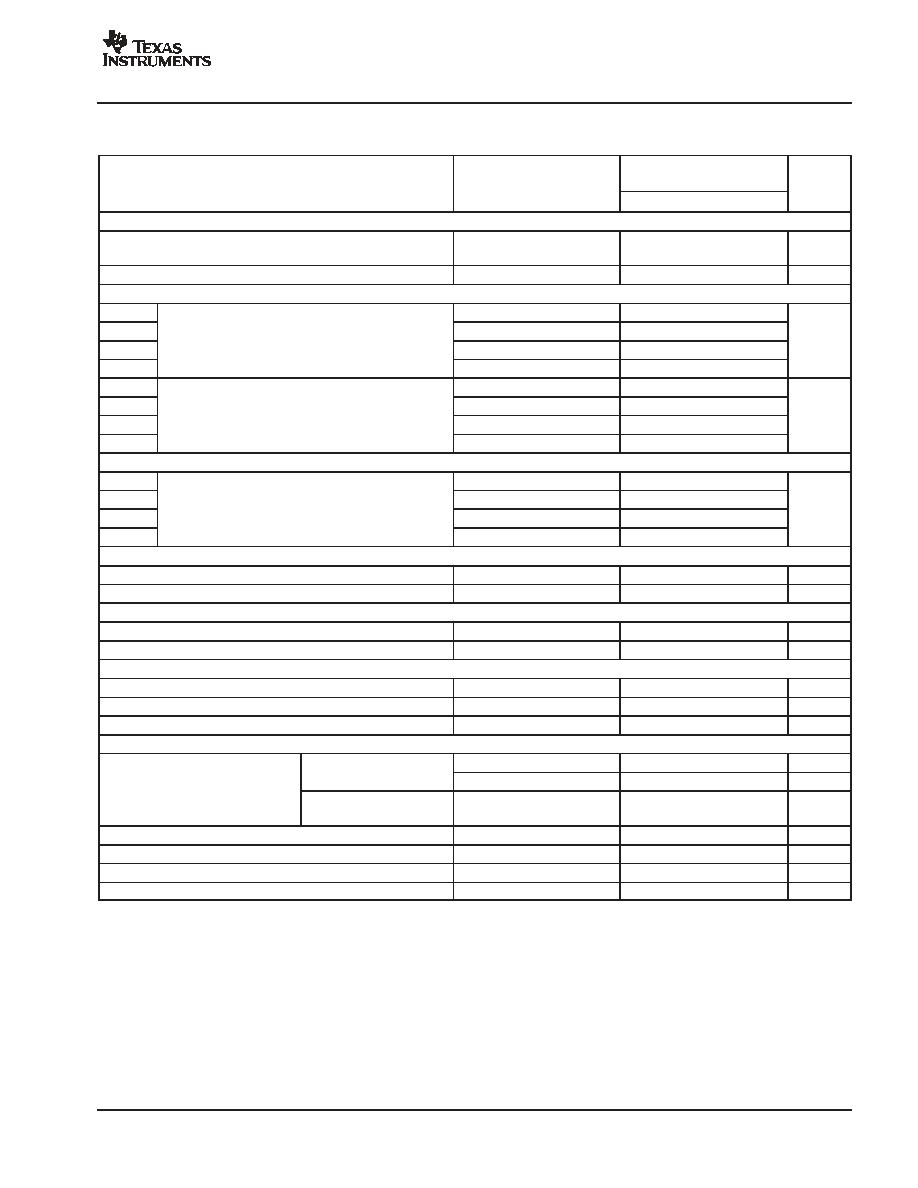
PACKAGE ORDERING INFORMATION
(1)
PRODUCT
PACKAGE-LEAD
PACKAGE CODE
OPERATING
TEMPERATURE
RANGE
PACKAGE
MARKING
ORDERING
NUMBER
TRANSPORT
MEDIA
PCM2704DB
SSOP-28
28DB
≠25
∞
C to 85
∞
C
PCM2704
PCM2704DB
Tube
PCM2704DB
SSOP-28
28DB
≠25
∞
C to 85
∞
C
PCM2704
PCM2704DBR
Tape and reel
PCM2705DB
SSOP-28
28DB
≠25
∞
C to 85
∞
C
PCM2705
PCM2705DB
Tube
PCM2705DB
SSOP-28
28DB
≠25
∞
C to 85
∞
C
PCM2705
PCM2705DBR
Tape and reel
PCM2706PJT
TQFP-32
32PJT
≠25
∞
C to 85
∞
C
PCM2706
PCM2706PJT
Tray
PCM2706PJT
TQFP-32
32PJT
≠25
∞
C to 85
∞
C
PCM2706
PCM2706PJTR
Tape and reel
PCM2707PJT
TQFP-32
32PJT
≠25
∞
C to 85
∞
C
PCM2707
PCM2707PJT
Tray
PCM2707PJT
TQFP-32
32PJT
≠25
∞
C to 85
∞
C
PCM2707
PCM2707PJTR
Tape and reel
(1) For the most current specification and package information, refer to our Web site at www.ti.com.
ABSOLUTE MAXIMUM RATINGS
over operating free-air temperature range unless otherwise noted(1)
UNITS
Supply voltage
VBUS
≠0.3 V to 6.5 V
Supply voltage
VCCP, VCCL, VCCR, VDD
≠0.3 V to 4 V
Supply voltage differences
VCCP, VCCL, VCCR, VDD
±
0.1 V
Ground voltage differences
PGND, AGNDL, AGNDR, DGND, ZGND
±
0.1 V
HOST
≠0.3 V to 6.5 V
Digital input voltage
D+, D≠, HID0/MS, HID1/MC, HID2/MD, XTI, XTO, DOUT, SSPND, CK, DT,
PSEL, FSEL, TEST, TEST0, TEST1, FUNC0, FUNC1, FUNC2, FUNC3
≠0.3 V to (VDD + 0.3) V < 4 V
VCOM
≠0.3 V to (VCCP + 0.3) V < 4 V
Analog input voltage
VOUTR
≠0.3 V to (VCCR + 0.3) V < 4 V
Analog input voltage
VOUTL
≠0.3 V to (VCCL + 0.3) V < 4 V
Input current (any pins except supplies)
±
10 mA
Ambient temperature under bias
≠40
∞
C to 125
∞
C
Storage temperature
≠55
∞
C to 150
∞
C
Junction temperature
150
∞
C
Lead temperature (soldering)
260
∞
C, 5 s
Package temperature (IR reflow, peak)
260
∞
C
(1) Stresses beyond those listed under "absolute maximum ratings" may cause permanent damage to the device. These are stress ratings only, and
functional operation of the device at these or any other conditions beyond those indicated under "recommended operating conditions" is not
implied. Exposure to absolute-maximum-rated conditions for extended periods may affect device reliability.
PCM2704, PCM2705
PCM2706, PCM2707
SLES081A - JUNE 2003 ≠ REVISED MAY 2004
www.ti.com
3
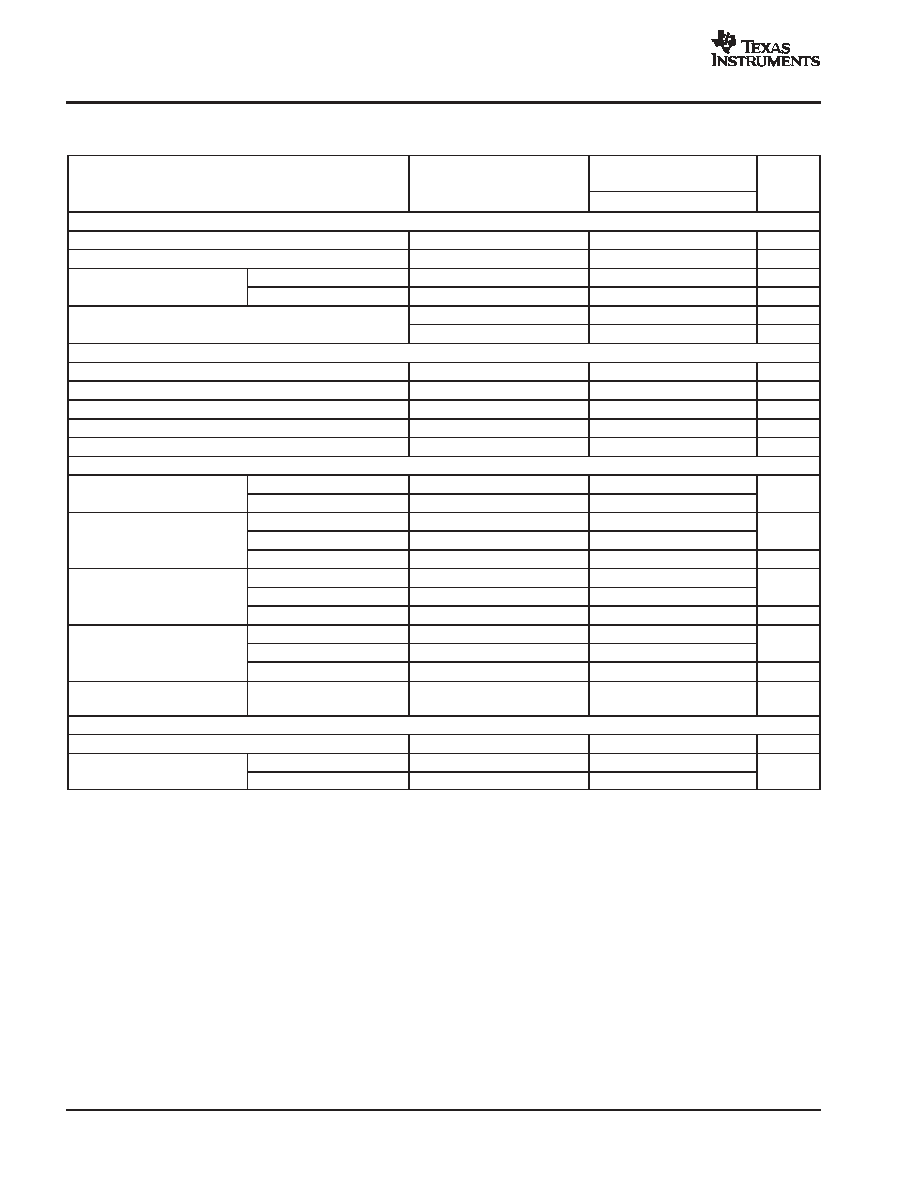
ELECTRICAL CHARACTERISTICS
all specifications at TA = 25
∞
C, VBUS = 5 V, fS = 44.1 kHz, fIN = 1 kHz,16-bit data, unless otherwise noted
PARAMETER
TEST CONDITIONS
PCM2704DB, PCM2705DB,
PCM2706PJT, PCM2707PJT
UNIT
PARAMETER
TEST CONDITIONS
MIN
TYP
MAX
UNIT
DIGITAL INPUT/OUTPUT
Host interface
Apply USB revision 1.1,
full-speed
Audio data format
USB isochronous data format
INPUT LOGIC
VIH
2
3.3
VIL
Input logic level
≠0.3
0.8
VDC
VIH(1)
Input logic level
2
5.5
VDC
VIL(1)
≠0.3
0.8
IIH(2)
VIN = 3.3 V
±
10
IIL(2)
Input logic current
VIN = 0 V
±
10
µ
A
IIH
Input logic current
VIN = 3.3 V
65
100
µ
A
IIL
VIN = 0 V
±
10
OUTPUT LOGIC
VOH(3)
IOH = ≠2 mA
2.8
VOL(3)
Output logic level
IOL = 2 mA
0.3
VDC
VOH
Output logic level
IOH = ≠2 mA
2.4
VDC
VOL
IOL = 2 mA
0.4
CLOCK FREQUENCY
Input clock frequency, XTI
11.994
12
12.006
MHz
fs
Sampling frequency
32, 44.1, 48
kHz
DAC CHARACTERISTICS
Resolution
16
Bits
Audio data channel
1, 2
Channel
DC ACCURACY
Gain mismatch, channel-to-channel
±
2
±
8
% of FSR
Gain error
±
2
±
8
% of FSR
Bipolar zero error
±
3
±
6
% of FSR
DYNAMIC PERFORMANCE(4)
Line(5)
RL > 10 k
, self-powered
0.006%
0.01%
THD+N,
V
= 0 dB
Line(5)
RL > 10 k
, bus-powered
0.012%
0.02%
THD+N,
VOUT = 0 dB
Headphone
RL = 32
,
self-/bus-powered
0.025%
THD+N, VOUT = ≠60 dB
2%
Dynamic range
EIAJ, A-weighted
90
98
dB
S/N ratio
EIAJ, A-weighted
90
98
dB
Channel separation
60
70
dB
(1) HOST
(2) D+, D≠, HOST, TEST, TEST0, TEST1, DT, PSEL, FSEL, XTI
(3) FUNC0, FUNC1, FUNC2
(4) fIN = 1 kHz, using the System Two
t
Cascade audio measurement system by Audio Precision
t
in the RMS mode with a 20-kHz LPF and 400-Hz
HPF.
(5) THD+N performance varies slightly depending on the effective output load, including dummy load R7, R8 in Figure 31.
System Two and Audio Precision are trademarks of Audio Precision, Inc.
PCM2704, PCM2705
PCM2706, PCM2707
SLES081A - JUNE 2003 ≠ REVISED MAY 2004
www.ti.com
4
ELECTRICAL CHARACTERISTICS (CONTINUED)
all specifications at TA = 25
∞
C, VBUS = 5 V, fS = 44.1 kHz, fIN = 1 kHz,16-bit data, unless otherwise noted
PARAMETER
TEST CONDITIONS
PCM2704DB, PCM2705DB,
PCM2706PJT, PCM2707PJT
UNIT
PARAMETER
TEST CONDITIONS
MIN
TYP
MAX
UNIT
ANALOG OUTPUT
Output voltage
0.55 VCCL, 0.55 VCCR
Vp-p
Center voltage
0.5 VCCP
V
Load impedance
Line
AC coupling
10
k
Load impedance
Headphone
AC coupling
16
32
LPF frequency
≠3 dB
140
kHz
LPF frequency
response
f = 20 kHz
≠0.1
dB
DIGITAL FILTER PERFORMANCE
Pass band
0.454 fs
Hz
Stop band
0.546 fs
Hz
Pass-band ripple
±
0.04
dB
Stop-band attenuation
≠50
dB
Delay time
20/fs
s
POWER SUPPLY REQUIREMENTS
Voltage range
VBUS
Bus-powered
4.35
5
5.25
VDC
Voltage range
VCCP, VCCL, VCCR, VDD
Self-powered
3
3.3
3.6
VDC
Line
DAC operation
23
30
mA
Supply current
Headphone
DAC operation (RL = 32
)
35
46
mA
Supply current
Line/headphone
Suspend mode (1)
150
190
µ
A
Power dissipation
Line
DAC operation
76
108
mW
Power dissipation
(self-powered)
Headphone
DAC operation (RL = 32
)
116
166
mW
(self-powered)
Line/headphone
Suspend mode (1)
495
684
µ
W
Power dissipation
Line
DAC operation
115
158
mW
Power dissipation
(bus-powered)
Headphone
DAC operation (RL = 32
)
175
242
mW
(bus-powered)
Line/headphone
Suspend mode (1)
750
998
µ
W
Internal power
supply voltage (2)
VCCP, VCCL, VCCR, VDD
Bus-powered
3.2
3.35
3.5
VDC
TEMPERATURE RANGE
Operating temperature
≠25
85
∞
C
JA
Thermal resistance
28-pin SSOP (PCM2704/5)
100
∞
C/W
JA
Thermal resistance
32-pin TQFP (PCM2706/7)
80
∞
C/W
(1) Under USB suspend state.
(2) VDD, VCCP, VCCL, VCCR. These pins work as output pins of internal power supply for bus-powered operation.
PCM2704, PCM2705
PCM2706, PCM2707
SLES081A - JUNE 2003 ≠ REVISED MAY 2004
www.ti.com
5
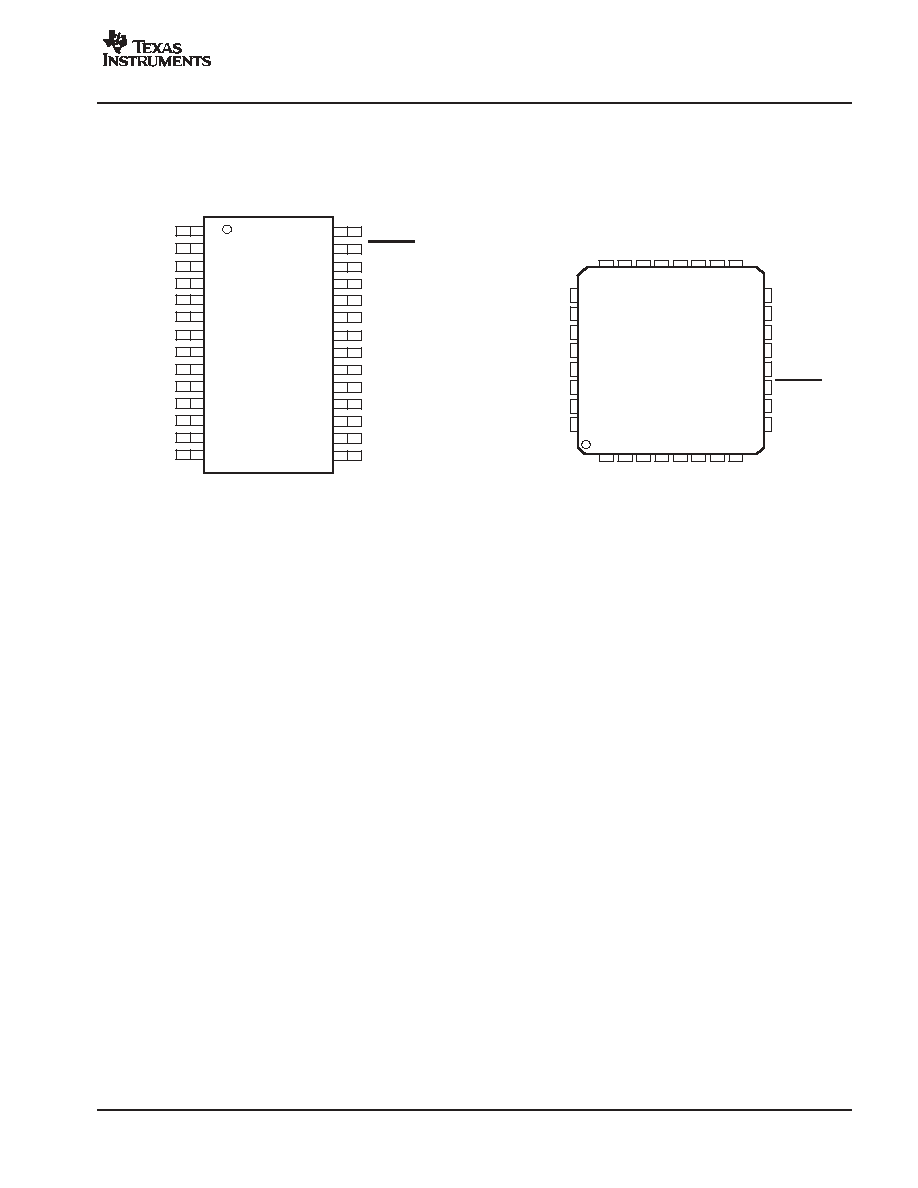
PIN ASSIGNMENTS
1
2
3
4
5
6
7
8
9
10
11
12
13
14
28
27
26
25
24
23
22
21
20
19
18
17
16
15
XTO
CK
DT
PSEL
DOUT
DGND
V
DD
D≠
D+
V
BUS
ZGND
AGNDL
V
CCL
V
OUT
L
XTI
SSPND
TEST0
TEST1
HID2/MD
HID1/MC
HID0/MS
HOST
V
CCP
PGND
V
COM
AGNDR
V
CCR
V
OUT
R
PCM2704/PCM2705
DB PACKAGE
(TOP VIEW)
PCM2706/PCM2707
PJT PACKAGE
(TOP VIEW)
23 22 21 20 19
1 2
25
26
27
28
29
30
31
32
16
15
14
13
12
11
10
9
PSEL
DT
CK
XTO
XTI
SSPND
TEST
FSEL
ZGND
AGNDL
V
CCL
V
OUT
L
V
OUT
R
V
CCR
AGNDR
V
COM
24
18
3
4
5 6 7
8
17
V
BUS
D+
D≠
V
DD
DGND
FUNC1
FUNC2
DOUT
PGND
V
CCP
HOST
FUNC3
FUNC0
HID0/MS
HID1/MC
HID2/MD