Document Outline
- FEATURES
- APPLICATIONS
- DESCRIPTION
- PACKAGING ORDERING INFORMATION
- ABSOLUTE MAXIMUM RATINGS
- ELECTRICAL CHARACTERISTICS
- PIN ASSIGNMENTS
- PCM2900 Terminal Functions
- PCM2902 Terminal Functions
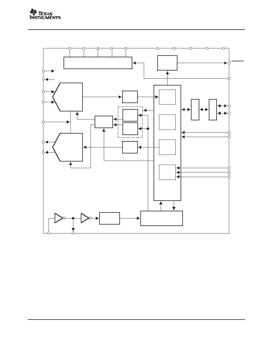
- PCM2900 FUNCTIONAL BLOCK DIAGRAM
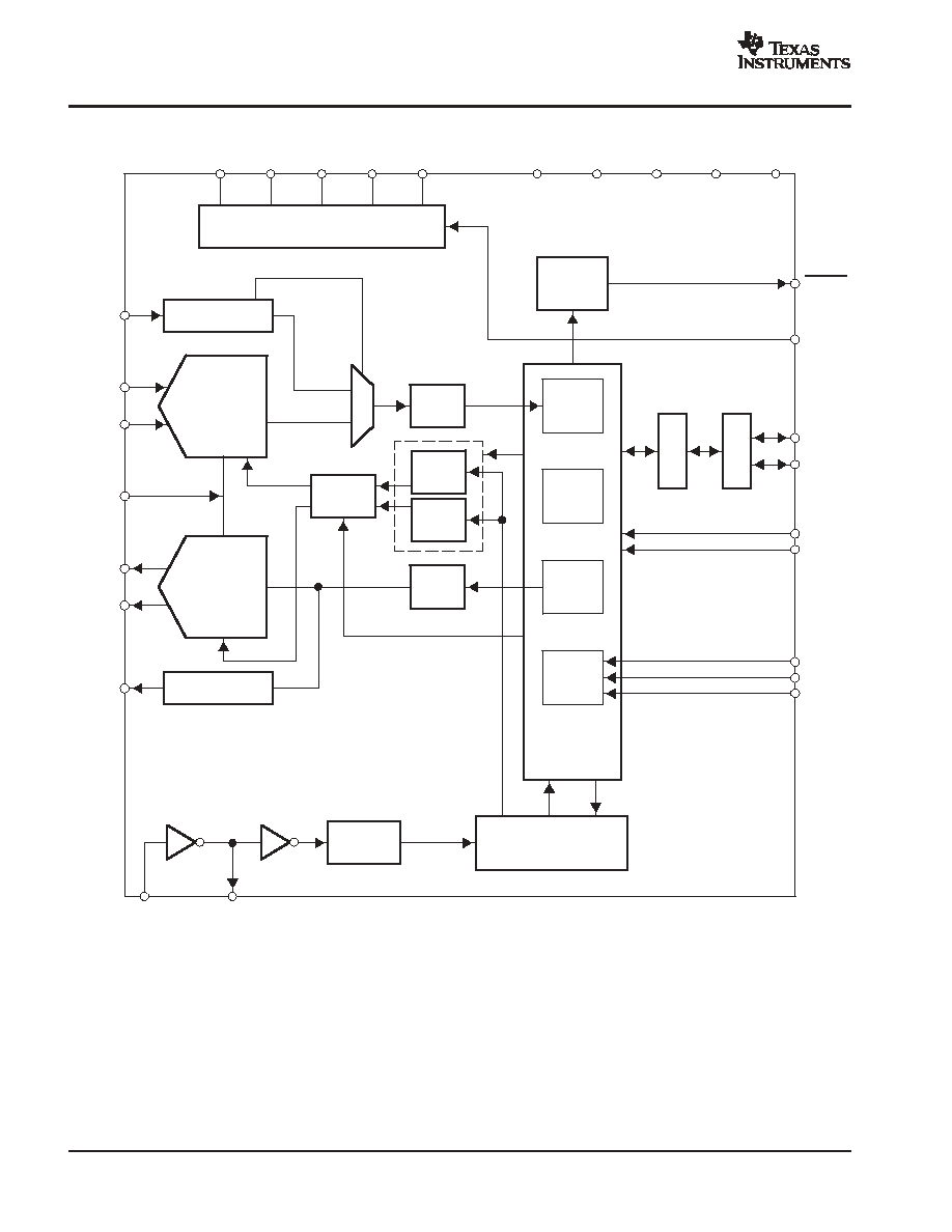
- PCM2902 FUNCTIONAL BLOCK DIAGRAM
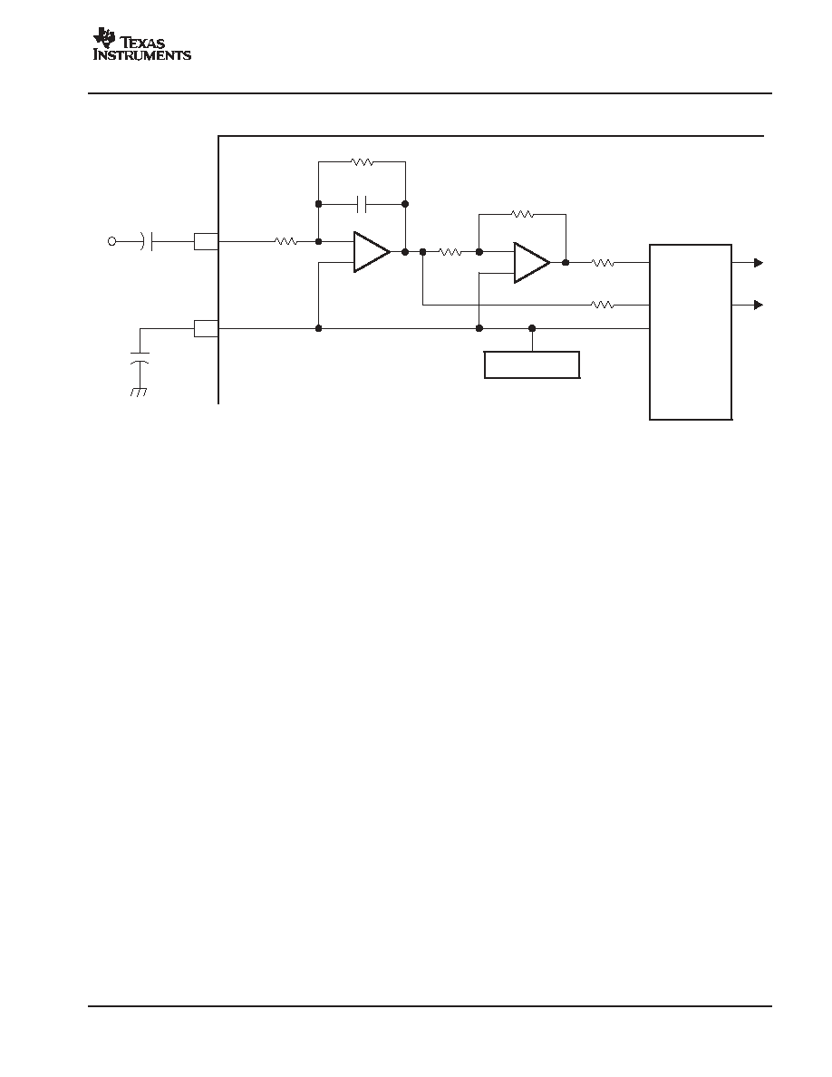
- PCM2900/2902 BLOCK DIAGRAM OF ANALOG FRONT-END (RIGHT CHANNEL)
- TYPICAL CHARACTERISTICS
- ADC
- DAC
- SUPPLY CURRENT
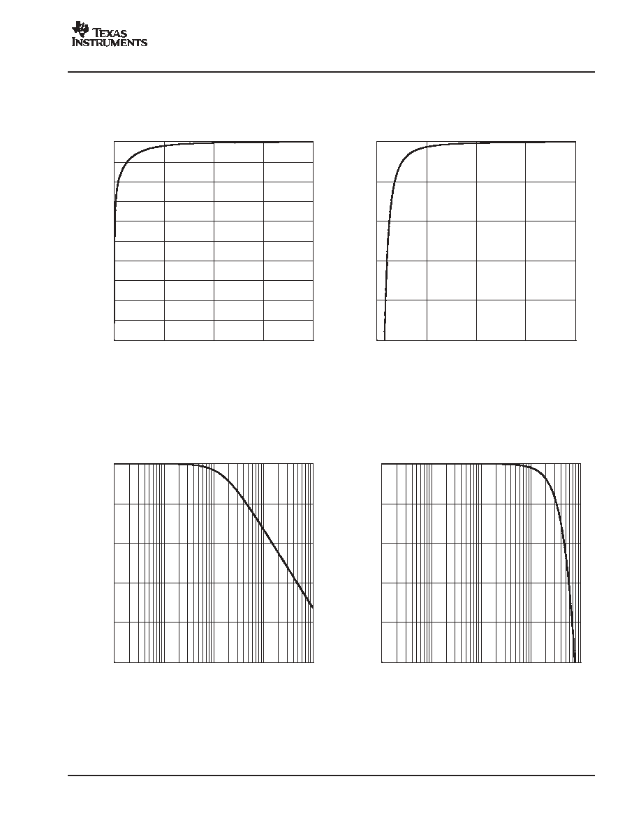
- ADC DIGITAL DECIMATION FILTER FREQUENCY RESPONSE
- ADC DIGITAL HIGH-PASS FILTER FREQUENCY RESPONSE
- ADC ANALOG ANTIALIASING FILTER FREQUENCY RESPONSE
- DAC DIGITAL INTERPOLATION FILTER FREQUENCY RESPONSE
- DAC ANALOG FIR FILTER FREQUENCY RESPONSE
- DAC ANALOG LOW-PASS FILTER FREQUENCY RESPONSE
- USB INTERFACE
- DEVICE CONFIGURATION
- Interface #0
- Interface #1
- Interface #2
- Interface #3
- End-Points
- Clock and Reset
- Digital Audio Interface (PCM2902)
- Supported Input Data (PCM2902)
- Channel Status Information (PCM2902)
- Copyright Management (PCM2902)
- INTERFACE SEQUENCE
- Power On, Attach, and Playback Sequence
- Play, Stop, and Detach Sequence
- Record Sequence
- Suspend and Resume Sequence
- PCM2900 TYPICAL CIRCUIT CONNECTION 1
- PCM2902 TYPICAL CIRCUIT CONNECTION 1
- PCM2900 TYPICAL CIRCUIT CONNECTION 2
- PCM2902 TYPICAL CIRCUIT CONNECTION 2
- APPLICATION INFORMATION
PCM2900
PCM2902
SLES035B - MARCH 2002 - REVISED JUNE 2004
STEREO AUDIO CODEC WITH USB INTERFACE,
SINGLE ENDED ANALOG INPUT/OUTPUT AND S/PDIF
FEATURES
D
PCM2900: Without S/PDIF
D
PCM2902: With S/PDIF
D
On-Chip USB Interface:
- With Full-Speed Transceivers
- Fully Compliant With USB 1.1
Specification
- Certified by USB-IF
- Partially Programmable Descriptors
(1)
- USB Adaptive Mode for Playback
- USB Asynchronous Mode for Record
- Bus Powered
D
16-Bit Delta Sigma ADC and DAC
D
Sampling Rate:
- DAC: 32, 44.1, 48 kHz
- ADC: 8, 11.025, 16, 22.05, 32, 44.1, 48 kHz
D
On-Chip Clock Generator:
- With Single 12-MHz Clock Source
D
Single Power Supply: 5 V TYP (V
BUS
)
D
Stereo ADC
- Analog Performance at V
BUS
= 5 V
- THD+N = 0.01%
- SNR = 89 dB
- Dynamic Range = 89 dB
- Decimation Digital Filter
- Pass-Band Ripple =
�
0.05 dB
- Stop-Band Attenuation = �65 dB
- Single-Ended Voltage Input
- Antialiasing Filter Included
- Digital LCF Included
D
Stereo DAC
- Analog Performance at V
BUS
= 5 V
- THD+N = 0.005%
- SNR = 96 dB
- Dynamic Range = 93 dB
- Oversampling Digital Filter
- Pass-Band Ripple =
�
0.1 dB
- Stop-Band Attenuation = �43 dB
- Single-Ended Voltage Output
- Analog LPF Included
D
Multifunctions:
- Human Interface Device (HID) Volume
�
Control and Mute Control
- Suspend Flag
D
Package: 28-Pin SSOP
APPLICATIONS
D
USB Audio Speaker
D
USB Headset
D
USB Monitor
D
USB Audio Interface Box
DESCRIPTION
The PCM2900/2902 is Texas Instruments single-chip
USB stereo audio codec with USB-compliant full-speed
protocol controller and S/PDIF (only PCM2902). The
USB protocol controller works with no software code,
but the USB descriptors can be modified in some areas
(e.g., vendor ID/product ID). The PCM2900/2902
employs SpAct
architecture, TI's unique system that
recovers the audio clock from USB packet data. On-chip
analog PLLs with SpAct enable playback and record with
low clock jitter and with independent playback and record
sampling rates.
PRODUCTION DATA information is current as of publication date. Products
conform to specifications per the terms of Texas Instruments standard warranty.
Production processing does not necessarily include testing of all parameters.
Burr Brown Products
from Texas Instruments
Please be aware that an important notice concerning availability, standard warranty, and use in critical applications of Texas Instruments
semiconductor products and disclaimers thereto appears at the end of this data sheet.
www.ti.com
Copyright
2004, Texas Instruments Incorporated
(1)The descriptor can be modified by changing a mask.
SpAct is a trademark of Texas Instruments, Incorporated.
Apple. Mac, and Mac OS are trademarks of Apple Computer, Inc.
Intel is a trademark of Intel Corporation.
Microsoft, Windows, Windows Me, and Windows XP are trademarks of Microsoft Corporation.
Other trademarks are the property of their respective owners.
PCM2900
PCM2902
SLES035B - MARCH 2002 - REVISED JUNE 2004
www.ti.com
2
This integrated circuit can be damaged by ESD. Texas Instruments recommends that all integrated circuits be handled with appropriate
precautions. Failure to observe proper handling and installation procedures can cause damage.
ESD damage can range from subtle performance degradation to complete device failure. Precision integrated circuits may be more
susceptible to damage because very small parametric changes could cause the device not to meet its published specifications.
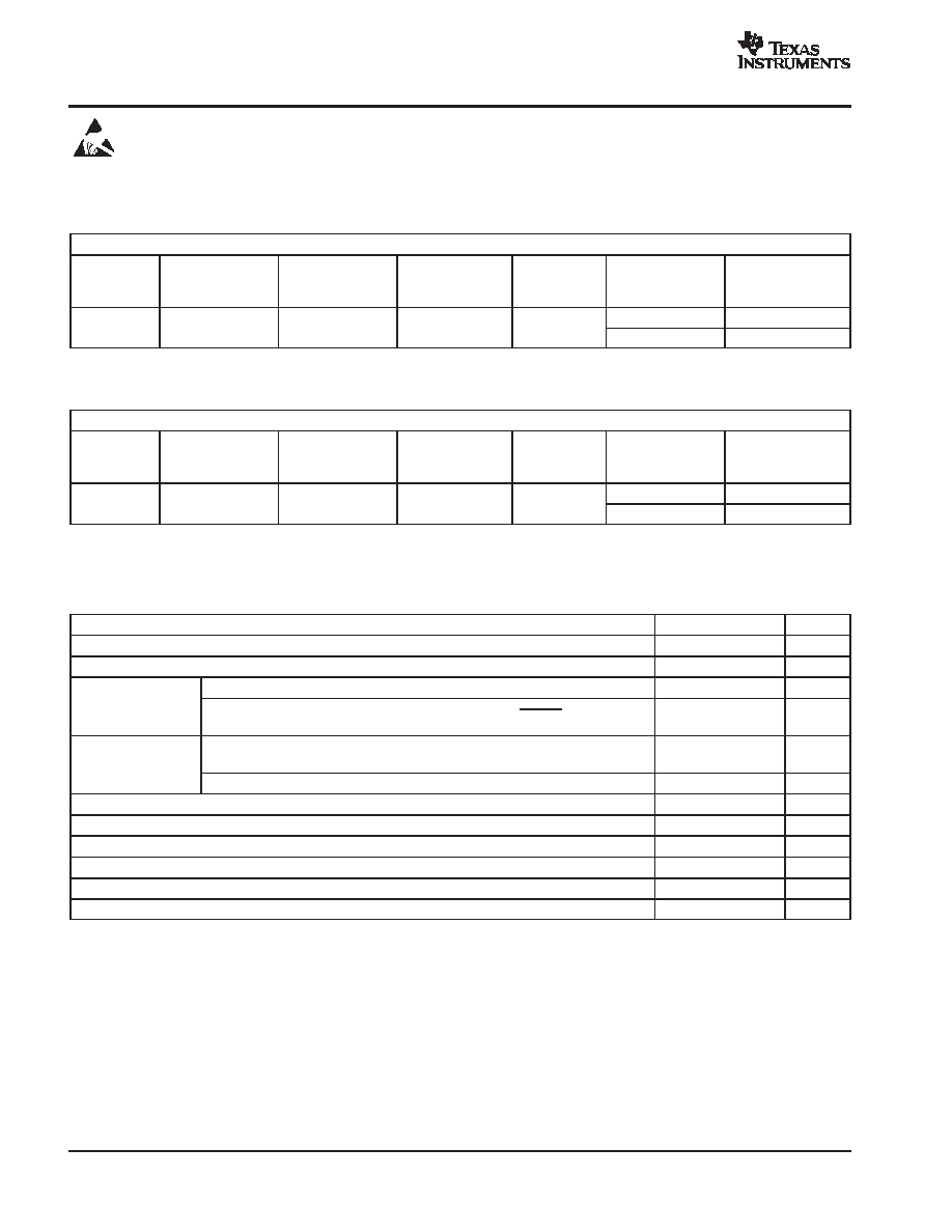
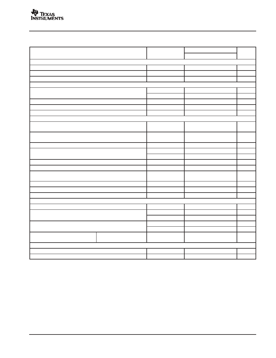
PACKAGING ORDERING INFORMATION
PCM2900
PRODUCT
PACKAGE-LEAD
PACKAGE
DESIGNATOR
SPECIFIED
TEMPERATURE
RANGE
PACKAGE
MARKING
ORDERING
NUMBER(1)
TRANSPORT
MEDIA
PCM2900E
SSOP-28
28DB
-25
�
C to 85
�
C
PCM2900E
PCM2900E
Rails
PCM2900E
SSOP-28
28DB
-25
�
C to 85
�
C
PCM2900E
PCM2900E/2K
Tape and reel
(1) Models with a slash (/) are available only in tape and reel in the quantities indicated (e.g., /2K indicates 2000 devices per reel). Ordering 2000
pieces of PCM2900E/2K gets a single 2000-piece tape and reel.
PCM2902
PRODUCT
PACKAGE-LEAD
PACKAGE
DESIGNATOR
SPECIFIED
TEMPERATURE
RANGE
PACKAGE
MARKING
ORDERING
NUMBER(1)
TRANSPORT
MEDIA
PCM2902E
SSOP-28
28DB
-25
�
C to 85
�
C
PCM2902E
PCM2902E
Rails
PCM2902E
SSOP-28
28DB
-25
�
C to 85
�
C
PCM2902E
PCM2902E/2K
Tape and reel
(1) Models with a slash (/) are available only in tape and reel in the quantities indicated (e.g., /2K indicates 2000 devices per reel). Ordering 2000
pieces of PCM2902E/2K gets a single 2000-piece tape and reel.
ABSOLUTE MAXIMUM RATINGS
over operating free-air temperature range unless otherwise noted(1)
PCM2900/PCM2902
UNIT
Supply voltage, VBUS
�0.3 to 6.5
V
Ground voltage differences, AGNDC, AGNDP, AGNDX, DGND, DGNDU
�
0.1
V
SEL0, SEL1, TEST0 (DIN)(2)
-0.3 to 6.5
V
Digital input voltage
D+, D�, HID0, HID1, HID2, XTI, XTO, TEST1 (DOUT)(2), SSPND
-0.3 to (VDDI + 0.3) <
4
V
Analog input voltage
VINL, VINR, VCOM, VOUTR, VOUTL
-0.3 to (VCCCI + 0.3)
< 4
V
Analog input voltage
VCCCI, VCCP1I, VCCP2I, VCCXI, VDDI
-0.3 to 4
V
Input current (any pins except supplies)
�
10
mA
Ambient temperature under bias
-40 to 125
�
C
Storage temperature, Tstg
-55 to 150
�
C
Junction temperature TJ
150
�
C
Lead temperature (soldering)
260
�
C, 5 s
Package temperature (IR reflow, peak)
250
�
C
(1) Stresses beyond those listed under "absolute maximum ratings" may cause permanent damage to the device. These are stress ratings only, and
functional operation of the device at these or any other conditions beyond those indicated under "recommended operating conditions" is not
implied. Exposure to absolute-maximum-rated conditions for extended periods may affect device reliability.
(2) ( ): PCM2902
PCM2900
PCM2902
SLES035B - MARCH 2002 - REVISED JUNE 2004
www.ti.com
3
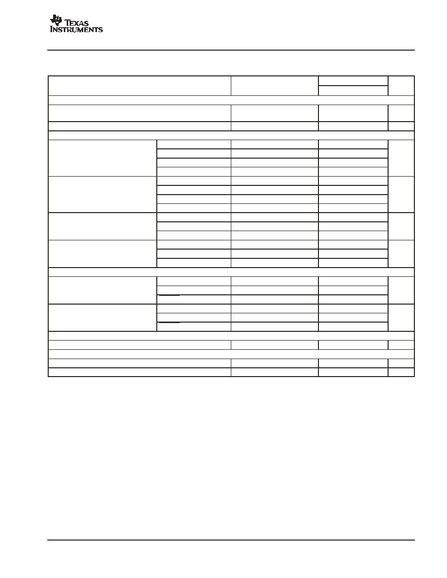
ELECTRICAL CHARACTERISTICS
all specifications at TA = 25
�
C, VBUS = 5 V, fS = 44.1 kHz, fIN = 1 kHz, 16-bit data, unless otherwise noted
PARAMETER
TEST CONDITIONS
PCM2900E, PCM2902E
UNIT
PARAMETER
TEST CONDITIONS
MIN
TYP
MAX
UNIT
Digital Input/Output
Host interface
Apply USB Revision 1.1,
full speed
Audio data format
USB isochronous data format
Input Logic
D+, D-
2
3.3
VIH
High-level input voltage
XTI, HID0, HID1, and HID2
2.52
3.3
VDC
VIH
High-level input voltage
SEL0, SEL1
2
5.25
VDC
DIN, PCM2902
2.52
5.25
D+, D-
0.8
VIL
Low-level input voltage
XTI, HID0, HID1, and HID2
0.9
VDC
VIL
Low-level input voltage
SEL0, SEL1
0.8
VDC
DIN, PCM2902
0.9
D+, D-, XTI, SEL0, SEL1
VIN = 3.3 V
�
10
IIH
High-level input current
HID0, HID1, and HID2
VIN = 3.3 V
50
80
�
A
IIH
High-level input current
DIN, PCM2902
VIN = 3.3 V
65
100
�
A
D+, D-, XTI, SEL0, SEL1
VIN = 0 V
�
10
IIL
Low-level input current
HID0, HID1, and HID2
VIN = 0 V
�
10
�
A
IIL
Low-level input current
DIN, PCM2902
VIN = 0 V
�
10
�
A
Output Logic
D+, D-
2.8
VOH
High-level output voltage
DOUT, PCM2902
IOH = �4 mA
2.8
VDC
VOH
High-level output voltage
SSPND
IOH = �2 mA
2.8
VDC
D+, D-
0.3
VOL
Low-level output voltage
DOUT, PCM2902
IOL = 4 mA
0.5
VDC
VOL
Low-level output voltage
SSPND
IOL = 2 mA
0.5
VDC
Clock Frequency
Input clock frequency, XTI
11.994
12
12.006
MHz
ADC Characteristics
Resolution
8, 16
bits
Audio data channel
1, 2
channel
PCM2900
PCM2902
SLES035B - MARCH 2002 - REVISED JUNE 2004
www.ti.com
4
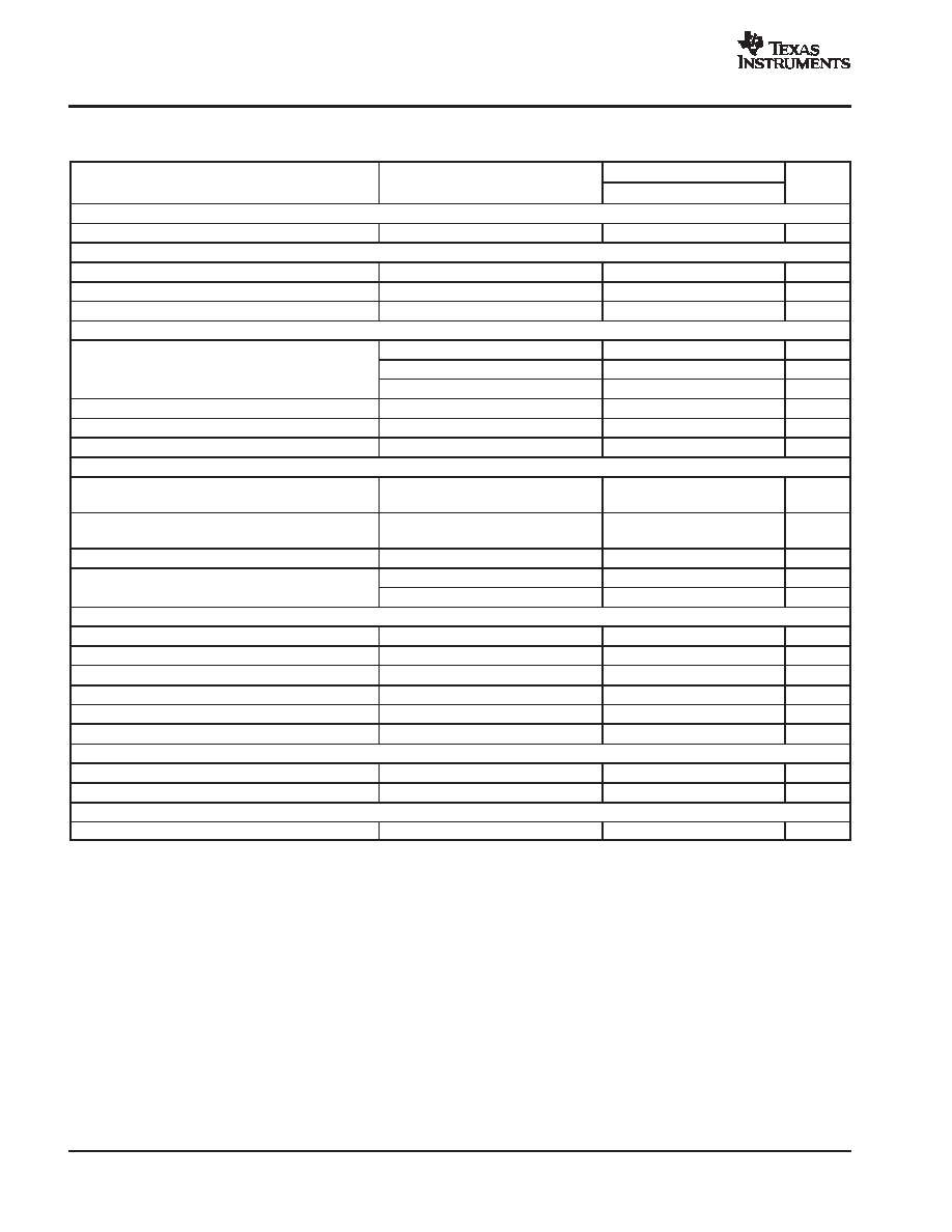
ELECTRICAL CHARACTERISTICS
all specifications at TA = 25
�
C, VBUS = 5 V, fS = 44.1 kHz, fIN = 1 kHz, 16-bit data, unless otherwise noted
PARAMETER
TEST CONDITIONS
PCM2900E, PCM2902E
UNIT
PARAMETER
TEST CONDITIONS
MIN
TYP
MAX
UNIT
Clock Frequency
fS
Sampling frequency
8, 11.025, 16, 22.05, 32, 44.1, 48
kHz
DC Accuracy
Gain mismatch channel-to-channel
�
1
�
5
% of FSR
Gain error
�
2
�
10
% of FSR
Bipolar zero error
�
0
% of FSR
Dynamic Performance(1)
VCCCI = 3.67 V, VIN = �0.5 dB(2)
0.01%
0.02%
THD+N
Total harmonic distortion plus noise
VIN = �0.5 dB(3)
0.1%
THD+N
Total harmonic distortion plus noise
VIN = �60 dB
5%
Dynamic range
A-weighted
81
89
dB
SNR
Signal-to-noise ratio
A-weighted
81
89
dB
Channel separation
80
85
dB
Analog Input
Input voltage
0.6
VCCCI
Vp-p
Center voltage
0.5
VCCCI
V
Input impedance
30
k
Antialiasing filter frequency response
�3 dB
150
kHz
Antialiasing filter frequency response
fIN = 20 kHz
�0.08
dB
Digital Filter Performance
Pass band
0.454 fS
Hz
Stop band
0.583 fS
Hz
Pass-band ripple
�
0.05
dB
Stop-band attenuation
�65
dB
td
Delay time
17.4/fS
s
LCF frequency response
�3 dB
0.078 fS
MHz
DAC Characteristics
Resolution
8, 16
bits
Audio data channel
1, 2
channel
Clock Frequency
fS
Sampling frequency
32, 44.1, 48
kHz
(1) fIN = 1 kHz, using Audio Precision System II, RMS mode with 20-kHz LPF, 400-Hz HPF in calculation.
(2) Using external voltage regulator for VCCCI (as shown in Figure 36 and Figure 37, using with REG103xA-A)
(3) Using internal voltage regulator for VCCCI (as shown in Figure 38 and Figure 39)
PCM2900
PCM2902
SLES035B - MARCH 2002 - REVISED JUNE 2004
www.ti.com
5
ELECTRICAL CHARACTERISTICS
all specifications at TA = 25
�
C, VBUS = 5 V, fS = 44.1 kHz, fIN = 1 kHz, 16-bit data, unless otherwise noted
PARAMETER
TEST CONDITIONS
PCM2900E, PCM2902E
UNIT
PARAMETER
TEST CONDITIONS
MIN
TYP
MAX
UNIT
DC Accuracy
Gain mismatch channel-to-channel
�
1
�
5
%of FSR
Gain error
�
2
�
10
% of FSR
Bipolar zero error
�
2
% of FSR
Dynamic Performance(1)
THD+N
Total harmonic distortion plus noise
VOUT = 0 dB
0.005%
0.016%
THD+N
Total harmonic distortion plus noise
VOUT = �60 dB
3%
Dynamic range
EIAJ, A-weighted
87
93
dB
SNR
Signal-to-noise ratio
EIAJ, A-weighted
90
96
dB
Channel separation
86
92
dB
Analog Output
VO
Output voltage
0.6
VCCCI
Vp-p
Center voltage
0.5
VCCCI
V
Load impedance
AC coupling
10
k
LPF frequency response
�3 dB
250
kHz
LPF frequency response
f = 20 kHz
�0.03
dB
Digital filter performance
Pass band
0.445 fS
Hz
Stop band
0.555
fS
Hz
Pass-band ripple
�
0.1
dB
Stop-band attenuation
�43
dB
td
Delay time
14.3 fS
s
Power Supply Requirements
VBUS
Voltage range
4.35
5
5.25
VDC
Supply current
ADC, DAC operation
56
67
mA
Supply current
Suspend mode(2)
210
�
A
PD
Power dissipation
ADC, DAC operation
280
352
mW
PD
Power dissipation
Suspend mode(2)
1.05
mW
Internal power supply voltage
VCCCI, VCCP1I,
VCCP2I, VCCXI, and VDDI
3.25
3.35
3.5
VDC
Temperature Range
Operation temperature
�25
85
_
C
JA
Thermal resistance
28-pin SSOP
100
�
C/W
(1) fOUT = 1 kHz, using Audio Precision System II, RMS mode with 20-kHz LPF, 400-Hz HPF.
(2) Under USB suspend state
PCM2900
PCM2902
SLES035B - MARCH 2002 - REVISED JUNE 2004
www.ti.com
6
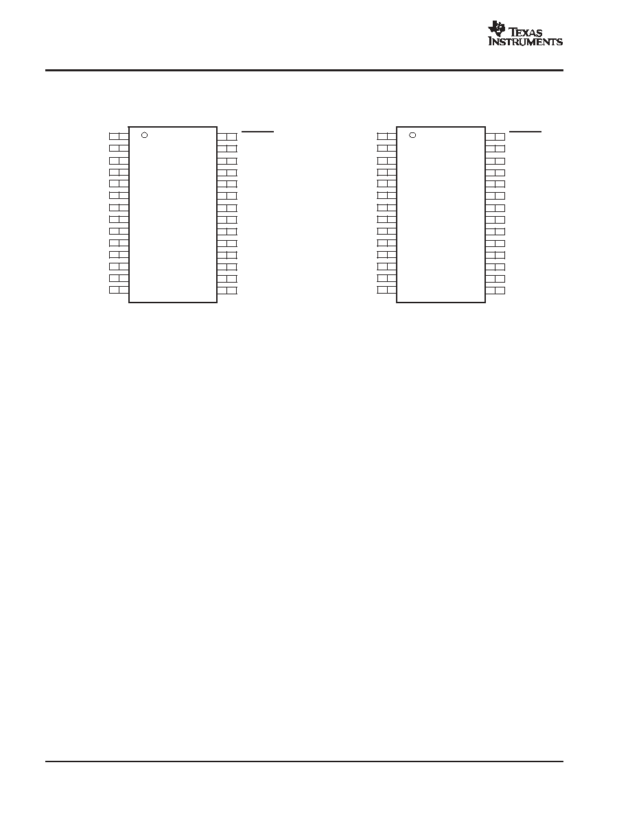
PIN ASSIGNMENTS
1
2
3
4
5
6
7
8
9
10
11
12
13
14
28
27
26
25
24
23
22
21
20
19
18
17
16
15
D+
D-
V
BUS
DGNDU
HID0
HID1
HID2
SEL0
SEL1
V
CCCI
AGNDC
V
IN
L
V
IN
R
V
COM
SSPND
V
DDI
DGND
TEST1
TEST0
V
CCXI
AGNDX
XTI
XTO
V
CCP2I
AGNDP
V
CCP1I
V
OUT
L
V
OUT
R
PCM2900
(TOP VIEW)
1
2
3
4
5
6
7
8
9
10
11
12
13
14
28
27
26
25
24
23
22
21
20
19
18
17
16
15
D+
D-
V
BUS
DGNDU
HID0
HID1
HID2
SEL0
SEL1
V
CCCI
AGNDC
V
IN
L
V
IN
R
V
COM
SSPND
V
DDI
DGND
DOUT
DIN
V
CCXI
AGNDX
XTI
XTO
V
CCP2I
AGNDP
V
CCP1I
V
OUT
L
V
OUT
R
PCM2902
(TOP VIEW)
PCM2900
PCM2902
SLES035B - MARCH 2002 - REVISED JUNE 2004
www.ti.com
7
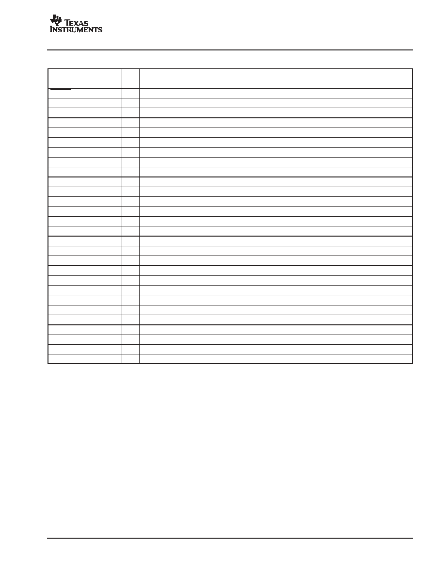
PCM2900 Terminal Functions
TERMINAL
I/O
DESCRIPTION
NAME
NO.
I/O
DESCRIPTION
SSPND
28
O
Suspend flag, active low (Low: suspend, High: operational)
AGNDC
11
-
Analog ground for codec
AGNDP
18
-
Analog ground for PLL
AGNDX
22
-
Analog ground for oscillator
D�
2
I/O
USB differential input/output minus(1)
D+
1
I/O
USB differential input/output plus(1)
DGND
26
-
Digital ground
DGNDU
4
-
Digital ground for USB transceiver
HID0
5
I
HID key state input (mute), active high(3)
HID1
6
I
HID key state input (volume up), active high(3)
HID2
7
I
HID key state input (volume down), active high(3)
SEL0
8
I
Must be set to high(5)
SEL1
9
I
Must be set to high(5)
TEST0
24
I
Test pin, must be connected to GND
TEST1
25
O
Test pin, must be left open
VBUS
3
-
Connect to USB power (VBUS)
VCCCI
10
-
Internal analog power supply for codec(4)
VCCP1I
17
-
Internal analog power supply for PLL(4)
VCCP2I
19
-
Internal analog power supply for PLL(4)
VCCXI
23
-
Internal analog power supply for oscillator(4)
VCOM
14
-
Common for ADC/DAC (VCCCI/2) (4)
VDDI
27
-
Internal digital power supply(4)
VINL
12
I
ADC analog input for L-channel
VINR
13
I
ADC analog input for R-channel
VOUTL
16
O
DAC analog output for L-channel
VOUTR
15
O
DAC analog output for R-channel
XTI
21
I
Crystal oscillator input(2)
XTO
20
O
Crystal oscillator output
(1) LV-TTL level
(2) 3.3-V CMOS level input
(3) 3.3-V CMOS level input with internal pulldown. This pin informs the PC of serviceable control signals such as mute, volume up, or volume down,
which has no connection with the internal DAC or ADC directly. See the Interface #3 and End-Points sections.
(4) Connect a decouple capacitor to GND
(5) TTL Schmitt trigger, 5 V tolerant
PCM2900
PCM2902
SLES035B - MARCH 2002 - REVISED JUNE 2004
www.ti.com
8
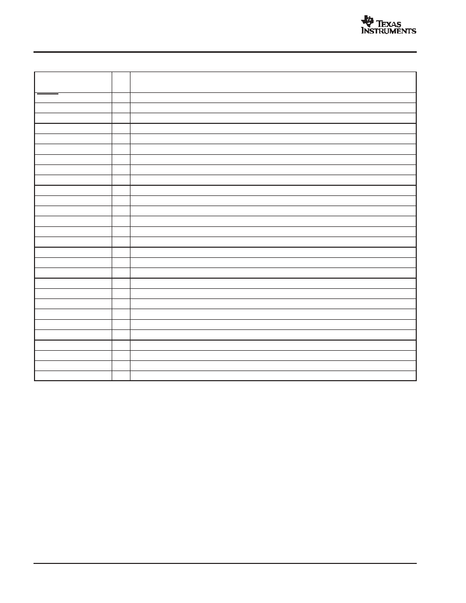
PCM2902 Terminal Functions
TERMINAL
I/O
DESCRIPTIONS
NAME
PIN
I/O
DESCRIPTIONS
SSPND
28
O
Suspend flag, active low (Low: suspend, High: operational)
AGNDC
11
-
Analog ground for codec
AGNDP
18
-
Analog ground for PLL
AGNDX
22
-
Analog ground for oscillator
D�
2
I/O
USB differential input/output minus(1)
D+
1
I/O
USB differential input/output plus(1)
DGND
26
-
Digital ground
DGNDU
4
-
Digital ground for USB transceiver
DIN
24
I
S/PDIF input(5)
DOUT
25
O
S/PDIF output
HID0
5
I
HID key state input (mute), active high(3)
HID1
6
I
HID key state input (volume up), active high(3)
HID2
7
I
HID key state input (volume down), active high(3)
SEL0
8
I
Must be set to high(6)
SEL1
9
I
Must be set to high(6)
VBUS
3
-
Connect to USB power (VBUS)
VCCCI
10
-
Internal analog power supply for codec(4)
VCCP1I
17
-
Internal analog power supply for PLL(4)
VCCP2I
19
-
Internal analog power supply for PLL(4)
VCCXI
23
-
Internal analog power supply for oscillator(4)
VCOM
14
-
Common for ADC/DAC (VCCCI/2) (4)
VDDI
27
-
Internal digital power supply(4)
VINL
12
I
ADC analog input for L-channel
VINR
13
I
ADC analog input for R-channel
VOUTL
16
O
DAC analog output for L-channel
VOUTR
15
O
DAC analog output for R-channel
XTI
21
I
Crystal oscillator input(2)
XTO
20
O
Crystal oscillator output
(1) LV-TTL level
(2) 3.3-V CMOS level input
(3) 3.3-V CMOS level input with internal pulldown. This pin informs the PC of serviceable control signals such as mute, volume up, or volume down,
which has no connection with the internal DAC or ADC directly. See the Interface #3 and End-Points sections.
(4) Connect a decouple capacitor to GND
(5) 3.3-V CMOS level input with internal pulldown, 5 V tolerant
(6) TTL Schmitt trigger, 5 V tolerant
PCM2900
PCM2902
SLES035B - MARCH 2002 - REVISED JUNE 2004
www.ti.com
9
PCM2900 FUNCTIONAL BLOCK DIAGRAM
SSPND
VCCCI VCCP1I VCCP2I VCCXI
VDDI
DGNDU
DGND
AGNDX
AGNDP
AGNDC
TEST1
ADC
VINL
VINR
VCOM
FIFO
Selector
Analog
PLL
Analog
PLL
FIFO
DAC
VOUTL
VOUTR
XTI
XTO
12 MHz
PLL (
y
8)
96 MHz
Tracker
(SpAct)
USB
Protocol
Controller
Power
Manager
ISO-In
End-Point
Control
End-Point
ISO-Out
End-Point
HID
End-Point
VBUS
USB SIE
D+
D-
XCVR
SEL0
SEL1
HID0
HID1
HID2
TEST0
5-V to 3.3-V Voltage Regulator
PCM2900
PCM2902
SLES035B - MARCH 2002 - REVISED JUNE 2004
www.ti.com
10
PCM2902 FUNCTIONAL BLOCK DIAGRAM
SSPND
S/PDIF Decoder
DIN
Lock
ADC
VINL
VINR
VCOM
FIFO
Selector
Analog
PLL
Analog
PLL
FIFO
DAC
VOUTL
VOUTR
S/PDIF Encoder
DOUT
XTI
XTO
12 MHz
PLL (
y
8)
96 MHz
Tracker
(SpAct)
USB
Protocol
Controller
Power
Manager
ISO-In
End-Point
Control
End-Point
ISO-Out
End-Point
HID
End-Point
USB SIE
D+
D-
XCVR
SEL0
SEL1
HID0
HID1
HID2
VBUS
5-V to 3.3-V Voltage Regulator
VCCCI VCCP1I VCCP2I VCCXI
VDDI
DGNDU
DGND
AGNDX
AGNDP
AGNDC
PCM2900
PCM2902
SLES035B - MARCH 2002 - REVISED JUNE 2004
www.ti.com
11
PCM2900/2902 BLOCK DIAGRAM OF ANALOG FRONT-END (RIGHT CHANNEL)
VINR
13
14
VCOM
+
+
4.7
�
F
30 k
+
-
+
-
Delta-Sigma
Modulator
(+)
(-)
Reference
(VCCCI/2)
10
�
F
PCM2900
PCM2902
SLES035B - MARCH 2002 - REVISED JUNE 2004
www.ti.com
12
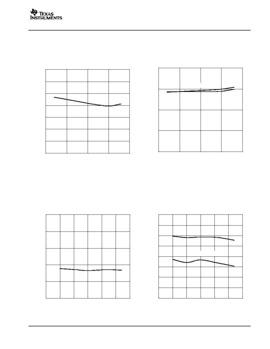
TYPICAL CHARACTERISTICS
ADC
Figure 1
0.03
0.04
0.05
0.06
0.07
0.08
0.09
0.10
-50
-25
0
25
50
75
100
TA - Free-Air Temperature -
�
C
THD+N - T
otal Harmonic Distortion + Noise - %
TOTAL HARMONIC DISTORTION + NOISE at -0.5 dB
vs
FREE-AIR TEMPERATURE
0.010
0.009
0.004
0.003
0.005
0.008
0.007
0.006
Figure 2
75
80
85
90
95
-50
-25
0
25
50
75
100
TA - Free-Air Temperature -
�
C
Dynamic Range and SNR - dB
DYNAMIC RANGE and SNR
vs
FREE-AIR TEMPERATURE
SNR
Dynamic Range
Figure 3
0.03
0.04
0.05
0.06
0.07
0.08
0.09
0.10
4.0
4.5
5.0
5.5
VBUS - Supply Voltage - V
THD+N - T
otal Harmonic Distortion + Noise - %
TOTAL HARMONIC DISTORTION + NOISE at -0.5 dB
vs
SUPPLY VOLTAGE
0.010
0.009
0.004
0.003
0.005
0.008
0.007
0.006
Figure 4
75
80
85
90
95
4.0
4.5
5.0
5.5
VBUS - Supply Voltage - V
Dynamic Range and SNR - dB
DYNAMIC RANGE and SNR
vs
SUPPLY VOLTAGE
SNR
Dynamic Range
All specifications at TA = 25
�
C, VBUS = 5 V, fS = 44.1 kHz, fin = 1 kHz, 16-bit data, using REG 103xA-A, unless otherwise noted.
PCM2900
PCM2902
SLES035B - MARCH 2002 - REVISED JUNE 2004
www.ti.com
13
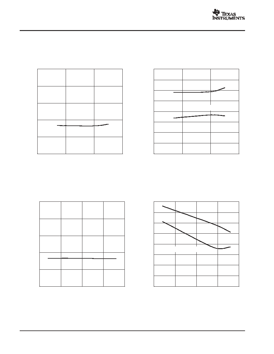
ADC (CONTINUED)
Figure 5
0.03
0.04
0.05
0.06
0.07
0.08
0.09
0.10
30
35
40
45
50
fS - Sampling Frequency - kHz
THD+N - T
otal Harmonic Distortion + Noise - %
TOTAL HARMONIC DISTORTION + NOISE at -0.5 dB
vs
SAMPLING FREQUENCY
0.010
0.009
0.004
0.003
0.005
0.008
0.007
0.006
Figure 6
75
80
85
90
95
30
35
40
45
50
fS - Sampling Frequency - kHz
Dynamic Range and SNR - dB
DYNAMIC RANGE and SNR
vs
SAMPLING FREQUENCY
SNR
Dynamic Range
DAC
Figure 7
0.03
0.04
0.05
0.06
0.07
0.08
-50
-25
0
25
50
75
100
TA - Free-Air Temperature -
�
C
THD+N - T
otal Harmonic Distortion + Noise - %
TOTAL HARMONIC DISTORTION + NOISE at 0 dB
vs
FREE-AIR TEMPERATURE
0.008
0.004
0.003
0.005
0.007
0.006
Figure 8
90
91
92
93
94
95
96
97
98
-50
-25
0
25
50
75
100
TA - Free-Air Temperature -
�
C
Dynamic Range and SNR - dB
DYNAMIC RANGE and SNR
vs
FREE-AIR TEMPERATURE
SNR
Dynamic Range
All specifications at TA = 25
�
C, VBUS = 5 V, fS = 44.1 kHz, fin = 1 kHz, 16-bit data, using REG 103xA-A, unless otherwise noted.
PCM2900
PCM2902
SLES035B - MARCH 2002 - REVISED JUNE 2004
www.ti.com
14
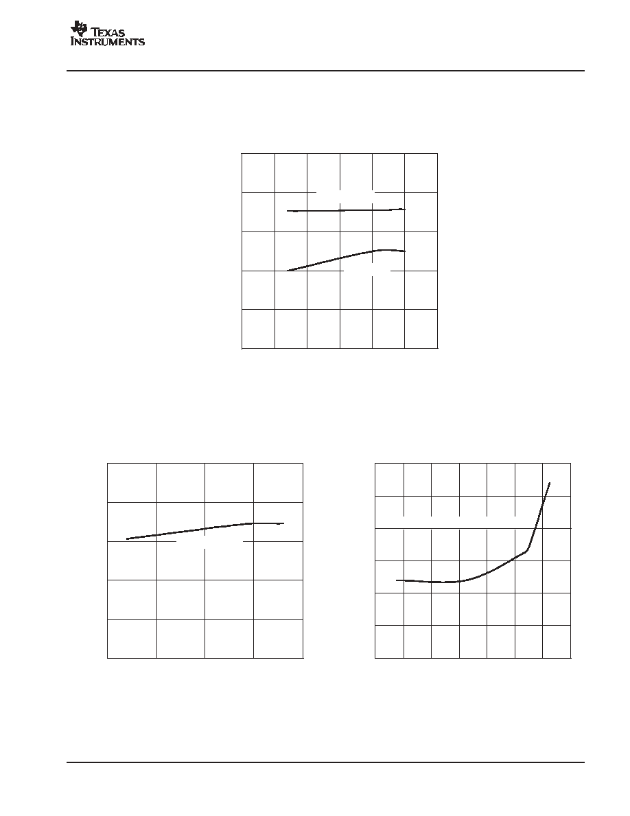
DAC (CONTINUED)
Figure 9
0.03
0.04
0.05
0.06
0.07
0.08
4.0
4.5
5.0
5.5
VBUS - Supply Voltage - V
THD+N - T
otal Harmonic Distortion + Noise - %
TOTAL HARMONIC DISTORTION + NOISE at 0 dB
vs
SUPPLY VOLTAGE
0.008
0.004
0.003
0.005
0.007
0.006
Figure 10
90
91
92
93
94
95
96
97
98
4.0
4.5
5.0
5.5
VBUS - Supply Voltage - V
Dynamic Range and SNR - dB
DYNAMIC RANGE and SNR
vs
SUPPLY VOLTAGE
SNR
Dynamic Range
Figure 11
0.03
0.04
0.05
0.06
0.07
0.08
30
35
40
45
50
fS - Sampling Frequency - kHz
THD+N - T
otal Harmonic Distortion + Noise - %
TOTAL HARMONIC DISTORTION + NOISE at 0 dB
vs
SAMPLING FREQUENCY
0.008
0.004
0.003
0.005
0.007
0.006
Figure 12
90
91
92
93
94
95
96
97
98
30
35
40
45
50
fS - Sampling Frequency - kHz
Dynamic Range and SNR - dB
DYNAMIC RANGE and SNR
vs
SAMPLING FREQUENCY
SNR
Dynamic Range
All specifications at TA = 25
�
C, VBUS = 5 V, fS = 44.1 kHz, fin = 1 kHz, 16-bit data, using REG 103xA-A, unless otherwise noted.
PCM2900
PCM2902
SLES035B - MARCH 2002 - REVISED JUNE 2004
www.ti.com
15
SUPPLY CURRENT
I CC
- Suspend Supply Current - mA
20
30
40
50
60
70
4.00
4.25
4.50
4.75
5.00
5.25
5.50
VBUS - Supply Voltage - V
I CC
- Operational Supply Current - mA
OPERATIONAL and SUSPEND
SUPPLY CURRENT
vs
SUPPLY VOLTAGE
Operational
Suspend
0.30
0.28
0.22
0.20
0.26
0.24
Figure 13
Figure 14
20
30
40
50
60
70
30
35
40
45
50
fS - Sampling Frequency - kHz
I CC
- Operational Supply Current - mA
OPERATIONAL SUPPLY CURRENT
vs
SAMPLING FREQUENCY
ADC and DAC
Figure 15
0.10
0.15
0.20
0.25
0.30
0.35
0.40
-40
-20
0
20
40
60
80
100
TA - Free-Air Temperature -
�
C
I CC
- Suspend Supply Current - mA
SUSPEND SUPPLY CURRENT
vs
FREE-AIR TEMPERATURE
USB Spec Limit for Device (0.3 mA)
All specifications at TA = 25
�
C, VBUS = 5 V, fS = 44.1 kHz, fin = 1 kHz, 16-bit data, using REG 103xA-A, unless otherwise noted.
PCM2900
PCM2902
SLES035B - MARCH 2002 - REVISED JUNE 2004
www.ti.com
16
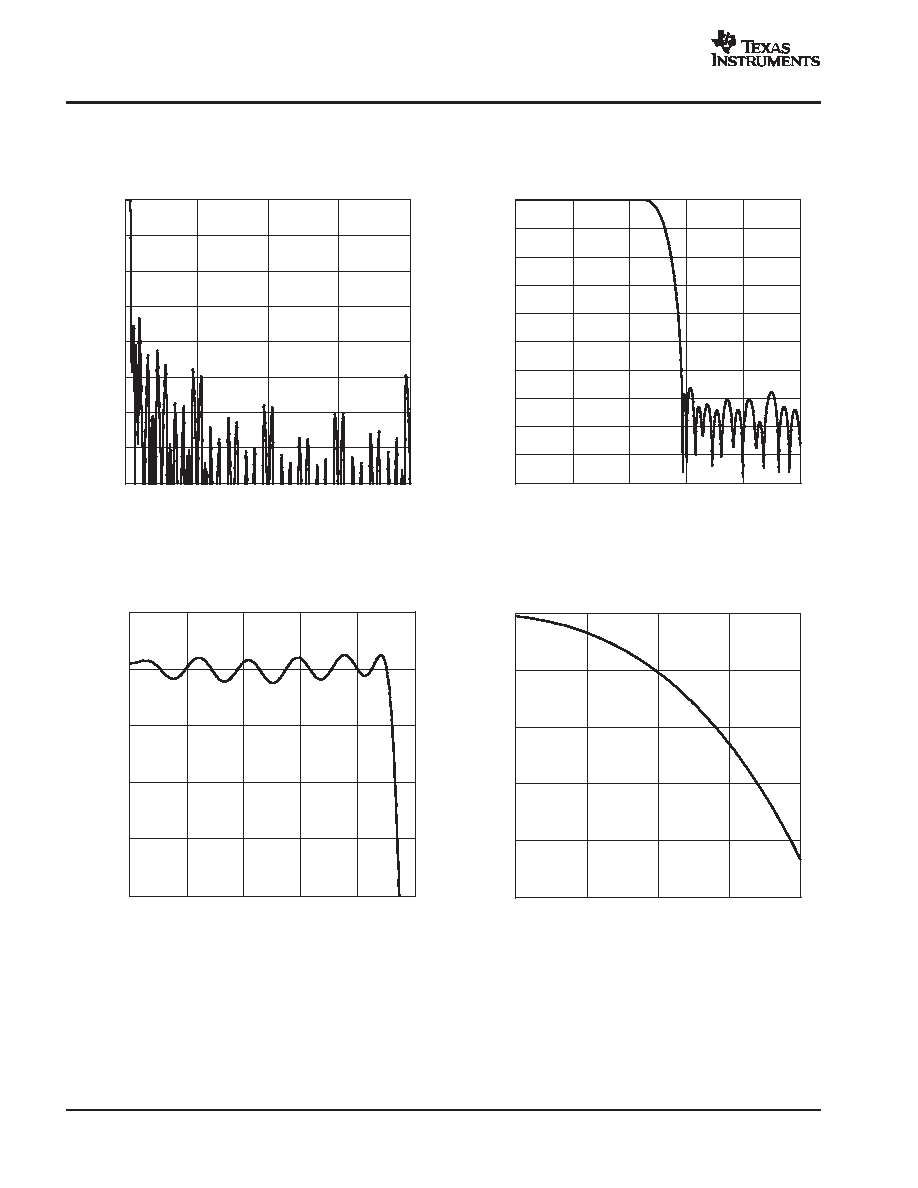
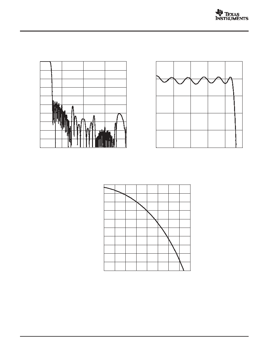
ADC DIGITAL DECIMATION FILTER FREQUENCY RESPONSE
Figure 16
Frequency [x fS]
-160
-140
-120
-100
-80
-60
-40
-20
0
0
8
16
24
32
Amplitude - dB
OVERALL CHARACTERISTICS
Figure 17
Frequency [x fS]
-100
-90
-80
-70
-60
-50
-40
-30
-20
-10
0
0.0
0.2
0.4
0.6
0.8
1.0
Amplitude - dB
STOP-BAND ATTENUATION
Figure 18
Frequency [x fS]
-0.8
-0.6
-0.4
-0.2
-0.0
0.2
0.0
0.1
0.2
0.3
0.4
0.5
Amplitude - dB
PASS-BAND RIPPLE
0.0
Figure 19
Frequency [x fS]
-20
-16
-12
-8
-4
0
0.46
0.48
0.50
0.52
0.54
Amplitude - dB
TRANSITION-BAND RESPONSE
All specifications at TA = 25
�
C, VBUS = 5 V, fS = 44.1 kHz, fin = 1 kHz, 16-bit data, unless otherwise noted.
PCM2900
PCM2902
SLES035B - MARCH 2002 - REVISED JUNE 2004
www.ti.com
17
ADC DIGITAL HIGH-PASS FILTER FREQUENCY RESPONSE
Figure 20
Frequency [x fS/1000]
-100
-90
-80
-70
-60
-50
-40
-30
-20
-10
0
0.0
0.1
0.2
0.3
0.4
Amplitude - dB
STOP-BAND CHARACTERISTIC
Figure 21
Frequency [x fS/1000]
-1.0
-0.8
-0.6
-0.4
-0.2
-0.0
0
1
2
3
4
Amplitude - dB
PASS-BAND CHARACTERISTIC
0.0
ADC ANALOG ANTIALIASING FILTER FREQUENCY RESPONSE
Figure 22
-50
-40
-30
-20
-10
0
f - Frequency - kHz
Amplitude - dB
STOP-BAND CHARACTERISTIC
1
100
1k
10k
10
Figure 23
-1.0
-0.8
-0.6
-0.4
-0.2
-0.0
f - Frequency - kHz
Amplitude - dB
PASS-BAND CHARACTERISTIC
0.01
1
10
100
0.1
0.0
All specifications at TA = 25
�
C, VBUS = 5 V, fS = 44.1 kHz, fin = 1 kHz, 16-bit data, unless otherwise noted.
PCM2900
PCM2902
SLES035B - MARCH 2002 - REVISED JUNE 2004
www.ti.com
18
DAC DIGITAL INTERPOLATION FILTER FREQUENCY RESPONSE
Figure 24
Frequency [x fS]
-100
-90
-80
-70
-60
-50
-40
-30
-20
-10
0
0
1
2
3
4
Amplitude - dB
STOP-BAND ATTENUATION
Figure 25
Frequency [x fS]
-0.8
-0.6
-0.4
-0.2
-0.0
0.2
0.0
0.1
0.2
0.3
0.4
0.5
Amplitude - dB
PASS-BAND RIPPLE
0.0
Frequency [x fS]
-20
-18
-16
-14
-12
-10
-8
-6
-4
-2
0
0.46
0.47
0.48
0.49
0.50
0.51
0.52
0.53
0.54
Amplitude - dB
TRANSITION-BAND RESPONSE
Figure 26
All specifications at TA = 25
�
C, VBUS = 5 V, fS = 44.1 kHz, fin = 1 kHz, 16-bit data, unless otherwise noted.
PCM2900
PCM2902
SLES035B - MARCH 2002 - REVISED JUNE 2004
www.ti.com
19
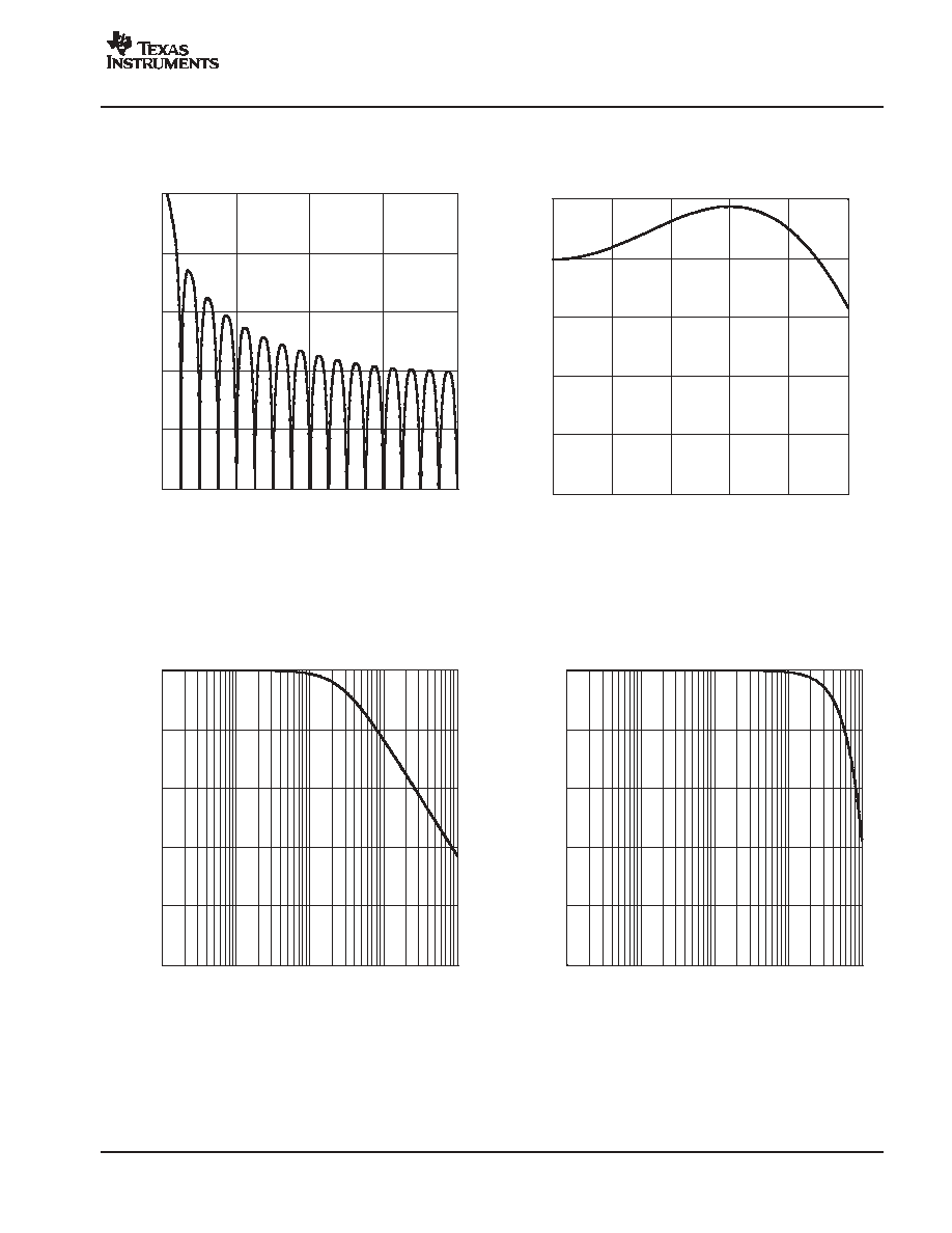
DAC ANALOG FIR FILTER FREQUENCY RESPONSE
Figure 27
-50
-40
-30
-20
-10
0
0
8
16
24
32
Frequency [x fS]
Amplitude - dB
STOP-BAND CHARACTERISTIC
Figure 28
-0.8
-0.6
-0.4
-0.2
-0.0
0.2
0.0
0.1
0.2
0.3
0.4
0.5
Frequency [x fS]
Amplitude - dB
PASS-BAND CHARACTERISTIC
0.0
DAC ANALOG LOW-PASS FILTER FREQUENCY RESPONSE
Figure 29
-50
-40
-30
-20
-10
0
f - Frequency - kHz
Amplitude - dB
STOP-BAND CHARACTERISTIC
1
100
1k
10k
10
Figure 30
-1.0
-0.8
-0.6
-0.4
-0.2
-0.0
f - Frequency - kHz
Amplitude - dB
PASS-BAND CHARACTERISTIC
0.01
1
10
100
0.1
0.0
All specifications at TA = 25
�
C, VBUS = 5 V, fS = 44.1 kHz, fin = 1 kHz, 16-bit data, unless otherwise noted.
PCM2900
PCM2902
SLES035B - MARCH 2002 - REVISED JUNE 2004
www.ti.com
20
USB INTERFACE
Control data and audio data are transferred to the PCM2900/2902 via D+ (pin 1) and D� (pin 2). All data to/from
the PCM2900/2902 is transferred at full speed. The device descriptor contains the information described in
Table 1. The device descriptor can be modified on request; contact a Texas Instruments representative for
details.
Table 1. Device Descriptor
USB revision
1.1 compliant
Device class
0x00 (device defined interface level)
Device sub class
0x00 (not specified)
Device protocol
0x00 (not specified)
Max packet size for end-point 0
8 byte
Vendor ID
0x08BB (default value, can be modified)
Product ID
0x2900 / 0x2902 (default value, can be modified)
Device release number
1.0 (0x0100)
Number of configurations
1
Vendor strings
String #1 (see Table 3)
Product strings
String #2 (see Table 3)
Serial number
Not supported
The configuration descriptor contains the information described in Table 2. The configuration descriptor can be
modified on request; contact a Texas Instruments representative for details.
Table 2. Configuration Descriptor
Interface
Four interfaces
Power attribute
0x80 (Bus powered, no remote wakeup)
Max power
0x32 (100 mA. Default value, can be modified)
The string descriptor contains the information described in Table 3. The string descriptor can be modified on
request; contact a Texas Instruments representative for details.
Table 3. String Descriptor
#0
0x0409
#1
Burr-Brown from TI (default value, can be modified)
#2
USB audio codec (default value, can be modified)
DEVICE CONFIGURATION
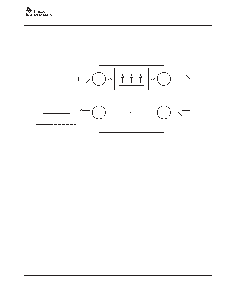
Figure 31 illustrates the USB audio function topology. The PCM2900/2902 has four interfaces. Each interface
is constructed by alternative settings.
PCM2900
PCM2902
SLES035B - MARCH 2002 - REVISED JUNE 2004
www.ti.com
21
Analog Out
Analog In
Default
End-Point
End-Point #2
(IF #1)
Audio Streaming
Interface
End-Point #0
End-Point #4
(IF #2)
Audio Streaming
Interface
End-Point #5
(IF #3)
HID Interface
IT
TID1
FU
UID3
OT
TID5
OT
TID2
IT
TID4
Standard Audio Control Interface (IF #0)
PCM2900/2902
Figure 31. USB Audio Function Topology
Interface #0
Interface #0 is defined as the control interface. Alternative setting #0 is the only possible setting for interface
#0. Alternative setting #0 describes the standard audio control interface. A terminal constructs the audio control
interface. The PCM2900/2902 has five terminals as follows:
D
Input terminal (IT #1) for isochronous-out stream
D
Output terminal (OT #2) for audio analog output
D
Feature unit (FU #3) for DAC digital attenuator
D
Input terminal (IT #4) for audio analog input
D
Output terminal (OT #5) for isochronous-in stream
Input terminal #1 is defined as USB stream (terminal type 0x0101). Input terminal #1 can accept 2-channel audio
streams constructed by left and right channels. Output terminal #2 is defined as a speaker (terminal type
0x0301). Input terminal #4 is defined as a microphone (terminal type 0x0201). Output terminal #5 is defined
as a USB stream (terminal type 0x0101). Output terminal #5 can generate 2-channel audio streams constructed
by left and right channels. Feature unit #3 supports the following sound control features.
D
Volume control
D
Mute control
The built-in digital volume controller can be manipulated by an audio class specific request from 0 dB to �64 dB
in 1-dB steps. Changes are made by incrementing or decrementing by one step (1 dB) for every 1/f
S
time interval
until the volume level has reached the requested value. Each channel can be set for different values. The master
PCM2900
PCM2902
SLES035B - MARCH 2002 - REVISED JUNE 2004
www.ti.com
22
volume control is not supported. A request to the master volume is stalled and ignored. The built-in digital mute
controller can be manipulated by audio class specific request. A master mute control request is acceptable. A
request to an individual channel is stalled and ignored.
Interface #1
Interface #1 is the audio streaming data-out interface. Interface #1 has the following seven alternative settings.
Alternative setting #0 is the zero bandwidth setting. All other alternative settings are operational settings.
ALTERNATIVE
SETTING
DATA FORMAT
TRANSFER
MODE
SAMPLING RATE
(kHz)
00
Zero Bandwidth
01
16 bit
Stereo
2s complement (PCM)
Adaptive
32, 44.1, 48
02
16 bit
Mono
2s complement (PCM)
Adaptive
32, 44.1, 48
03
8 bit
Stereo
2s complement (PCM)
Adaptive
32, 44.1, 48
04
8 bit
Mono
2s complement (PCM)
Adaptive
32, 44.1, 48
05
8 bit
Stereo
Offset binary (PCM8)
Adaptive
32, 44.1, 48
06
8 bit
Mono
Offset binary (PCM8)
Adaptive
32, 44.1, 48
Interface #2
Interface #2 is the audio streaming data-in the interface. Interface #2 has the following 19 alternative settings.
Alternative setting #0 is the zero bandwidth setting. All other alternative settings are operational settings.
ALTERNATIVE
SETTING
DATA FORMAT
TRANSFER
MODE
SAMPLING RATE
(kHz)
00
Zero Bandwidth
01
16 bit
Stereo
2s complement (PCM)
Asynchronous
48
02
16 bit
Mono
2s complement (PCM)
Asynchronous
48
03
16 bit
Stereo
2s complement (PCM)
Asynchronous
44.1
04
16 bit
Mono
2s complement (PCM)
Asynchronous
44.1
05
16 bit
Stereo
2s complement (PCM)
Asynchronous
32
06
16 bit
Mono
2s complement (PCM)
Asynchronous
32
07
16 bit
Stereo
2s complement (PCM)
Asynchronous
22.05
08
16 bit
Mono
2s complement (PCM)
Asynchronous
22.05
09
16 bit
Stereo
2s complement (PCM)
Asynchronous
16
0A
16 bit
Mono
2s complement (PCM)
Asynchronous
16
0B
8 bit
Stereo
2s complement (PCM)
Asynchronous
16
0C
8 bit
Mono
2s complement (PCM)
Asynchronous
16
0D
8 bit
Stereo
2s complement (PCM)
Asynchronous
8
0E
8 bit
Mono
2s complement (PCM)
Asynchronous
8
0F
16 bit
Stereo
2s complement (PCM)
Synchronous
11.025
10
16 bit
Mono
2s complement (PCM)
Synchronous
11.025
11
8 bit
Stereo
2s complement (PCM)
Synchronous
11.025
12
8 bit
Mono
2s complement (PCM)
Synchronous
11.025
Interface #3
Interface #3 is the interrupt data-in interface. Alternative setting #0 is the only possible setting for interface #3.
Interface #3 constructs the HID consumer control device and reports the following three key statuses.
D
Mute (0xE209)
D
Volume up (0xE909)
D
Volume down (0xEA09)

PCM2900
PCM2902
SLES035B - MARCH 2002 - REVISED JUNE 2004
www.ti.com
23
End-Points
The PCM2900/2902 has the following four end-points.
D
Control end-point (EP #0)
D
Isochronous-out audio data stream end-point (EP #2)
D
Isochronous-in audio data stream end-point (EP #4)
D
HID end-point (EP #5)
The control end-point is a default end-point. The control end-point is used to control all functions of the
PCM2900/2902 by the standard USB request and USB audio class specific request from the host. The
isochronous-out audio data stream end-point is an audio sink end-point, which receives the PCM audio data.
The isochronous-out audio data stream end-point accepts the adaptive transfer mode. The isochronous-in
audio data stream end-point is an audio source end-point, which transmits the PCM audio data. The
isochronous-in audio data stream end-point uses asynchronous transfer mode. The HID end-point is an
interrupt-in end-point. HID end-point reports HID0, HID1, and HID2 pin status every 32 ms.
The human interface device (HID) pins are defined as consumer control devices. The HID function is designed
as an independent end-point from both isochronous-in and -out end-points. This means that the result of
affection for the HID operation depends on the host software. Typically, the HID function is affected for the
primary audio-out device.
Clock and Reset
The PCM2900/2902 requires a 12-MHz (
�
500 ppm) clock for the USB and audio function, which can be
generated by a built-in crystal oscillator with a 12-MHz crystal resonator. The 12-MHz crystal resonator must
be connected to XTI (pin 21) and XTO (pin 20) with one high (1-M
) resistor and two small capacitors, the
capacitance of which depends on the load capacitance of the crystal resonator. The external clock can be
supplied from XTI (pin 21). If the external clock is supplied, XTO (pin 20) must be left open. Because of no
clock-disabling signal, it is not recommended to use the external clock supply. SSPND
(pin 28) is unable to use
clock disabling.
The PCM2900/2902 has an internal power-on reset circuit, which works automatically when V
BUS
(pin 3)
exceeds 2.5 V typical (2.7 V
�
2.2 V), and about 700
�
s is required until internal reset release.
Digital Audio Interface (PCM2902)
The PCM2902 employs both S/PDIF input and output. Isochronous-out data from the host is encoded to the
S/PDIF output and the DAC analog output. Input data is selected as either S/PDIF or ADC analog input. When
the device detects an S/PDIF input and successfully locks the received data, the isochronous-in transfer data
source is automatically selected from S/PDIF itself; otherwise, the data source is selected to ADC analog input.
Supported Input Data (PCM2902)
The following data formats are accepted by the S/PDIF input and output. All other data formats are unable to
use S/PDIF.
D
48-kHz 16-bit stereo
D
44.1-kHz 16-bit stereo
D
32-kHz 16-bit stereo
Mismatch between input data format and host command may cause unexpected results except in the following
conditions.
D
Record monaural format from stereo data input at the same data rate
D
Record 8-bit format from 16-bit data input at the same data rate
A combination between the above conditions is not accepted.
For the playback, all possible data rate source is converted to 16-bit stereo format at the same source data rate.
Channel Status Information (PCM2902)
The channel status information is fixed as consumer application, PCM mode, copyright, and digital/digital
converter. All other bits are fixed as 0s except for the sample frequency, which is set automatically according
to the data received through the USB.
PCM2900
PCM2902
SLES035B - MARCH 2002 - REVISED JUNE 2004
www.ti.com
24
Copyright Management (PCM2902)
Isochronous-in data is affected by the serial copy management system (SCMS). Where receiving digital audio
data that is indicated as original data in the control bit, input digital audio data transfers to the host. If the data
is indicated as first generation or higher, transferred data is selected to analog input.
Digital audio data output is always encoded as original with SCMS control.
The implementation of this feature is an option for the customer. Note that it is the user's responsibility whether
they implement this feature in their product or not.
INTERFACE SEQUENCE
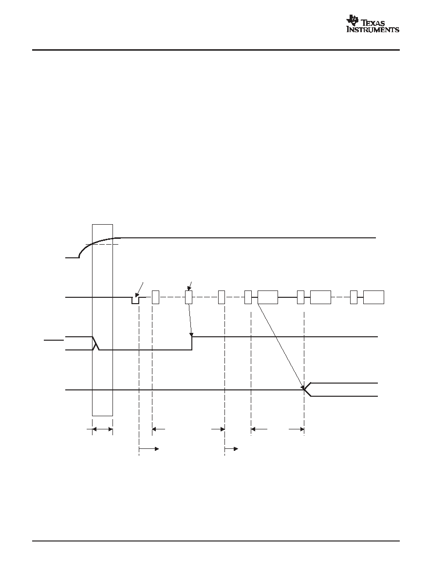
Power On, Attach, and Playback Sequence
The PCM2900/2902 is ready for setup when the reset sequence has finished and the USB bus is attached. After
connection has been established by setup, the PCM2900/2902 is ready to accept USB audio data. While
waiting, the audio data (idle state) and analog output are set to bipolar zero (BPZ).
When receiving the audio data, the PCM2900/2902 stores the first audio packet, which contained 1-ms audio
data, into the internal storage buffer. The PCM2900/2902 starts playing the audio data when detecting the
following start of frame (SOF) packet.
���
���
���
���
���
���
���
���
���
���
���
���
���
���
���
���
���
���
���
D+/D-
2.5 V (Typ.)
0 V
Internal Reset
Ready for Setup
��
��
��
���
���
���
SOF
���
���
���
�
�
�
���
���
���
��
��
��
Ready for Playback
��
��
��
��
��
��
Bus Reset
Set Configuration
SOF
SOF
��
��
��
BPZ
Bus Idle
5 V
(Typ.)
1st Audio Data
2nd Audio Data
VBUS (Pin 3)
SSPND
VOUTL
VOUTR
700
�
s
Device Setup
1 ms
Figure 32. Initial Sequence
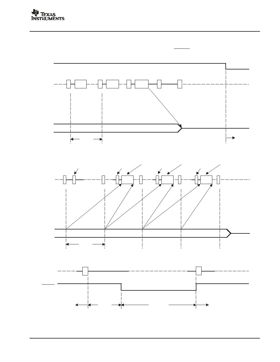
Play, Stop, and Detach Sequence
When the host finishes or aborts the playback, the PCM2900/2902 stops playing after the last audio data has
played.
Record Sequence
The PCM2900/2902 starts the audio capture into the internal memory after receiving the SET_INTERFACE
command.
PCM2900
PCM2902
SLES035B - MARCH 2002 - REVISED JUNE 2004
www.ti.com
25
Suspend and Resume Sequence
The PCM2900/2902 enters the suspend state after it sees a constant idle state on the USB bus, approximately
5 ms. While the PCM2900/2902 enters the suspend state, SSPND flag (pin 28) is asserted. The
PCM2900/2902 wakes up immediately when detecting the non-idle state on the USB bus.
D+/D-
VOUTL
VOUTR
Audio Data
Audio Data
Last Audio Data
Detach
SOF
SOF
SOF
SOF
SOF
1 ms
�
�
��
��
���
���
��
��
��
��
�
�
���
���
�
�
VBUS (Pin 3)
Figure 33. Play, Stop, and Detach
D+/D-
VINL
VINR
1 ms
SET_INTERFACE
Audio Data
IN Token
Audio Data
IN Token
Audio Data
IN Token
SOF
SOF
SOF
SOF
SOF
�
�
�
��
��
��
�
�
�
��
��
��
�
�
�
���
���
���
��
��
��
�
�
�
�
�
�
��
��
��
�
�
�
��
��
��
Figure 34. Record Sequence
5 ms
D+/D-
SSPND
Idle
��
��
��
��
Active
Active
Suspend
Figure 35. Suspend and Resume
PCM2900
PCM2902
SLES035B - MARCH 2002 - REVISED JUNE 2004
www.ti.com
26
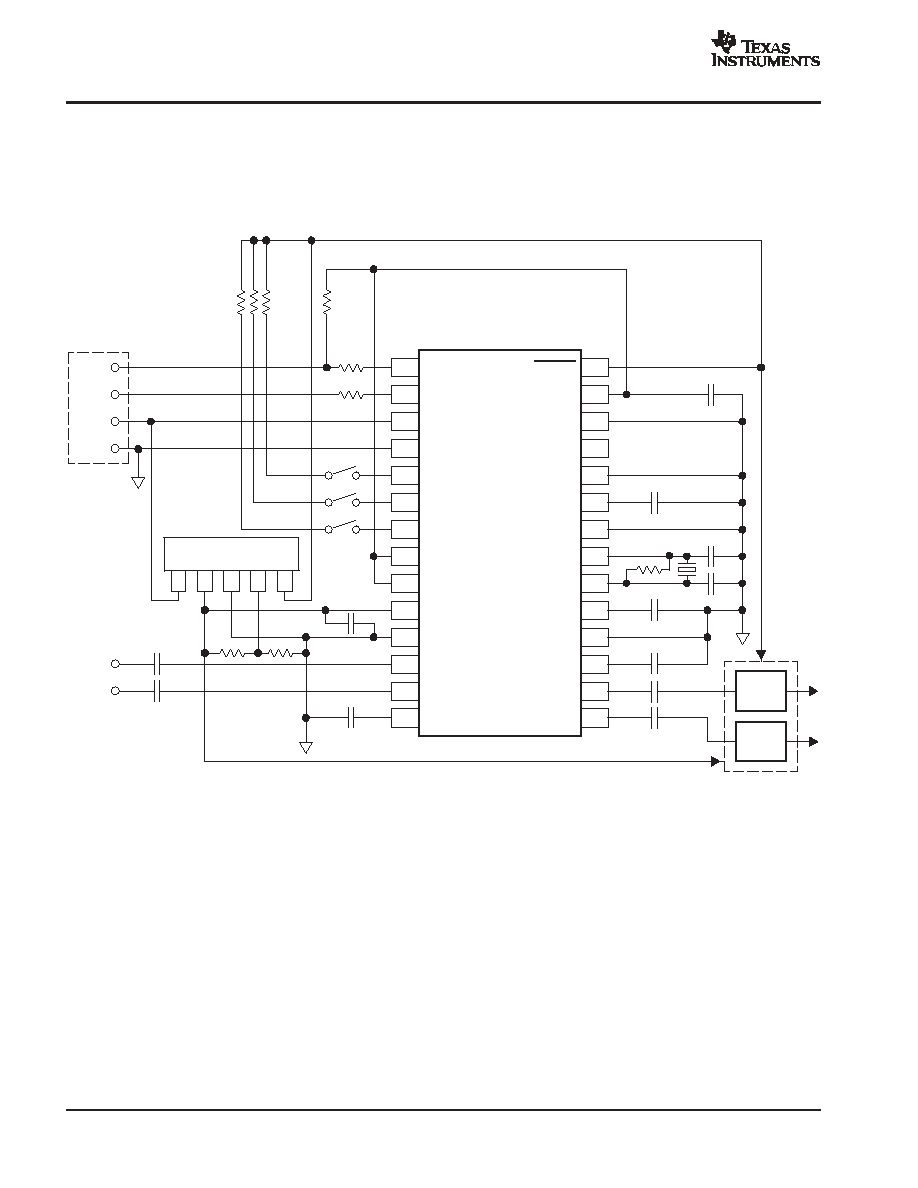
PCM2900 TYPICAL CIRCUIT CONNECTION 1
Figure 36 illustrates a typical circuit connection for a high-performance application. The circuit illustrated is for
information only. The whole board design should be considered to meet the USB specification as a
USB-compliant product.
NOTE: C1, C2: 10
�
F
C3, C4, C7, C8: 1
�
F (These capacitors must be less than 2
�
F)
C5, C6: 10 pF to 33 pF (depending on crystal resonator)
C9, C10, C11, C12: The capacitance may vary depending on design.
IC1: REG103xA-A (TI) or equivalent. Analog performance may vary depending on IC1.
D+
28
27
26
25
24
23
22
21
20
19
1
2
3
4
5
6
7
8
9
10
PCM2900
D-
VBUS
DGNDU
HID0
HID1
HID2
SEL0
SEL1
VCCCI
SSPND
XTI
VDDI
DGND
TEST1
TEST0
XTO
VCCP2I
AGNDX
VCCXI
D+
D-
MUTE/
Power
Down
C1
11
12
13
14
AGNDC
VINL
VINR
VCOM
18
17
16
15
VCCP1I
VOUTL
VOUTR
AGNDP
22
22
1.5 k
x 3
1.5 k
GND
VBUS
C2
C9
C10
1 M
12 MHz
C5
C6
C3
C8
C11
C12
LPF,
Amp
LPF,
Amp
C7
C4
3.6 V -
3.85 V
12 k
22 k
IN
1
OUT
2
GND
3
ADJ
4
EN
5
IC1
Figure 36. Bus-Powered Configuration for High-Performance Application
PCM2900
PCM2902
SLES035B - MARCH 2002 - REVISED JUNE 2004
www.ti.com
27
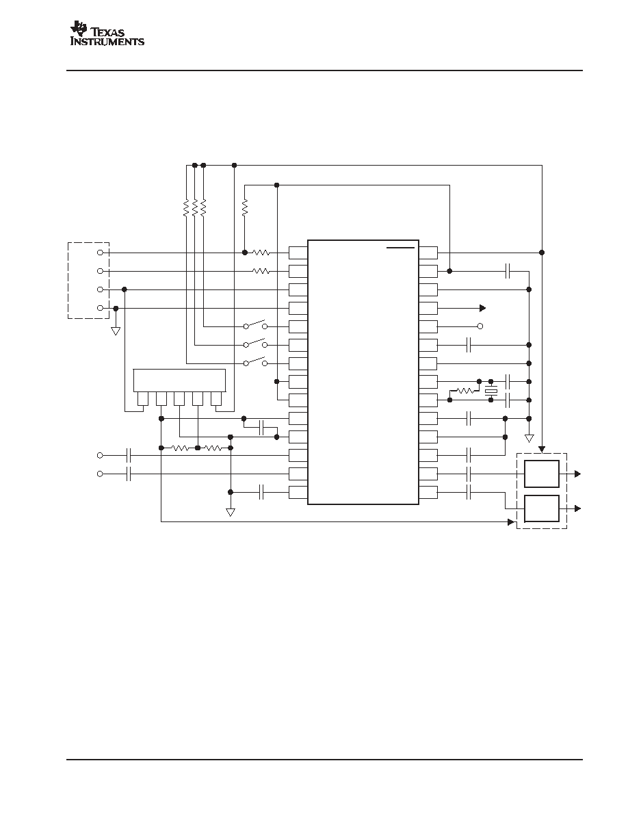
PCM2902 TYPICAL CIRCUIT CONNECTION 1
Figure 37 illustrates a typical circuit connection for a high-performance application. The circuit illustrated is for
information only. The whole board design should be considered to meet the USB specification as a
USB-compliant product.
NOTE: C1, C2: 10
�
F
C3, C4, C7, C8: 1
�
F (These capacitors must be less than 2
�
F)
C5, C6: 10 pF to 33 pF (depending on crystal resonator)
C9, C10, C11, C12: The capacitance may vary depending on design.
IC1: REG103xA-A (TI) or equivalent. Analog performance may vary depending on IC1.
D+
28
27
26
25
24
23
22
21
20
19
1
2
3
4
5
6
7
8
9
10
PCM2902
D-
VBUS
DGNDU
HID0
HID1
HID2
SEL0
SEL1
VCCCI
SSPND
XTI
VDDI
DGND
DOUT
DIN
XTO
VCCP2I
AGNDX
VCCXI
D+
D-
MUTE/
Power
Down
C1
11
12
13
14
AGNDC
VINL
VINR
VCOM
18
17
16
15
VCCP1I
VOUTL
VOUTR
AGNDP
22
22
1.5 k
x 3
1.5 k
GND
VBUS
C2
C9
C10
1 M
12 MHz
C5
C6
C3
C8
C11
C12
LPF,
Amp
LPF,
Amp
C7
C4
3.6 V -
3.85 V
12 k
22 k
IN
1
OUT
2
GND
3
ADJ
4
EN
5
IC1
Figure 37. Bus-Powered Configuration for High-Performance Application
PCM2900
PCM2902
SLES035B - MARCH 2002 - REVISED JUNE 2004
www.ti.com
28
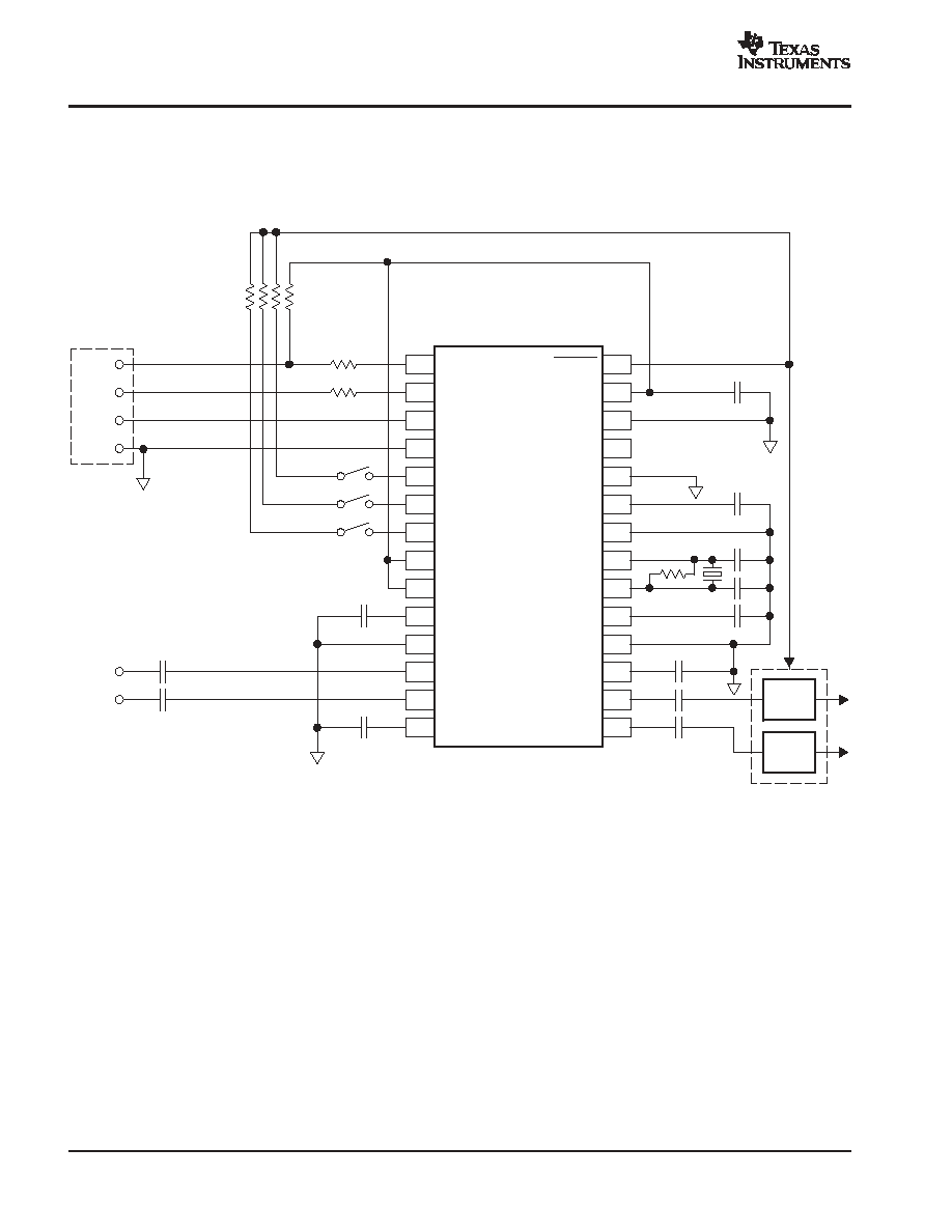
PCM2900 TYPICAL CIRCUIT CONNECTION 2
Figure 38 illustrates a typical circuit connection for a simple application. The circuit illustrated is for information
only. The whole board design should be considered to meet the USB specification as a USB-compliant product.
NOTE: C1, C2: 10
�
F
C3, C4, C7, C8: 1
�
F (These capacitors must be less than 2
�
F.)
C5, C6: 10 pF to 33 pF (depending on crystal resonator)
C9, C10, C11, C12: The capacitance may vary depending on design.
In this case analog perfomance of the A/D converter may degrade.
D+
28
27
26
25
24
23
22
21
20
19
1
2
3
4
5
6
7
8
9
10
PCM2900
D-
VBUS
DGNDU
HID0
HID1
HID2
SEL0
SEL1
VCCCI
SSPND
XTI
VDDI
DGND
TEST1
TEST0
XTO
VCCP2I
AGNDX
VCCXI
D+
D-
MUTE/
Power
Down
11
12
13
14
AGNDC
VINL
VINR
VCOM
18
17
16
15
VCCP1I
VOUTL
VOUTR
AGNDP
22
22
1.5 k
x 4
GND
VBUS
C2
C9
C10
1 M
12 MHz
C5
C6
C3
C8
C11
C12
LPF,
Amp
LPF,
Amp
C1
C7
C4
Figure 38. Bus-Powered Configuration
PCM2900
PCM2902
SLES035B - MARCH 2002 - REVISED JUNE 2004
www.ti.com
29
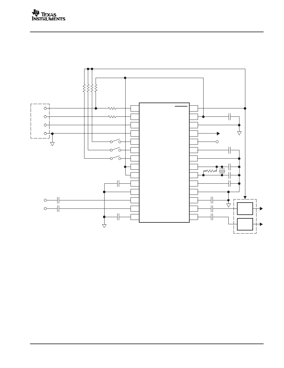
PCM2902 TYPICAL CIRCUIT CONNECTION 2
Figure 39 illustrates a typical circuit connection for a simple application. The circuit illustrated is for information
only. The whole board design should be considered to meet the USB specification as a USB-compliant product.
NOTE: C1, C2: 10
�
F
C3, C4, C7, C8: 1
�
F (These capacitors must be less than 2
�
F.)
C5, C6: 10 pF to 33 pF (depending on crystal resonator)
C9, C10, C11, C12: The capacitance may vary depending on design.
In this case analog perfomance of the A/D converter may degrade.
D+
28
27
26
25
24
23
22
21
20
19
1
2
3
4
5
6
7
8
9
10
PCM2902
D-
VBUS
DGNDU
HID0
HID1
HID2
SEL0
SEL1
VCCCI
SSPND
XTI
VDDI
DGND
DOUT
DIN
XTO
VCCP2I
AGNDX
VCCXI
D+
D-
MUTE/
Power
Down
11
12
13
14
AGNDC
VINL
VINR
VCOM
18
17
16
15
VCCP1I
VOUTL
VOUTR
AGNDP
22
22
1.5 k
x 4
GND
VBUS
C2
C9
C10
1 M
12 MHz
C5
C6
C3
C8
C11
C12
LPF,
Amp
LPF,
Amp
C1
C7
C4
Figure 39. Bus-Powered Configuration

PCM2900
PCM2902
SLES035B - MARCH 2002 - REVISED JUNE 2004
www.ti.com
30
APPLICATION INFORMATION
OPERATING ENVIRONMENT
To get the appropriate operation, one of the following operating systems must be working on the host PC that
has the USB port assured by the manufacturer. If the condition is fulfilled, the operation of the PCM2900/2902
does not depend on the operating speed of the CPU.
Texas Instruments has confirmed following operating environments.
D
Operating System
-
Microsoft
Windows
98/98SE/Me
Japanese/English Edition
-
Microsoft Windows 2000 Professional Japanese/English Edition
-
Microsoft Windows XP
Home/Professional Japanese/English Edition (For Windows
XP, use the
latest version of the USB audio driver that is available on Windows update site)
-
Apple
Computer Mac
OS 9.1 or later Japanese/English Edition
-
Apple Computer Mac OS
X 10.0 or later English Edition
-
Apple Computer Mac OS X 10.1 or later Japanese Edition (For Mac OS X 10.0 Japanese Edition, plug
and play does not work for USB audio device appropriately)
D
PC: Following PC-AT compatible computers for above OS (OS requirement must be met)
-
Motherboard using Intel
440BX or ZX chipset (using USB controller in the chipset)
-
Motherboard using Intel i810 chipset (using USB controller in the chipset)
-
Motherboard using Intel i815 chipset (using USB controller in the chipset)
-
Motherboard using Intel i820 chipset (using USB controller in the chipset)
-
Motherboard using Intel i845 chipset (using USB controller in the chipset)
-
Motherboard using Intel i850 chipset (using USB controller in the chipset)
-
Motherboard using Apollo KT133 chipset (using USB controller in the chipset)
-
Motherboard using Apollo Pro plus chipset (using USB controller in the chipset)
-
Motherboard using MVP4 or MVP3 chipset (using USB controller in the chipset)
-
Motherboard using Aladdin V chipset (using USB controller in the chipset)
-
Motherboard using SiS530 or SiS559 chipset (using USB controller in the chipset)
-
Motherboard using SiS735 chipset (using USB controller in the chipset)
NOTE: The OSs and PCs for which the operation of the PCM2900/2902 was confirmed are listed above. The PCM2900/2902 may also work with
other OSs and PCs that have not been tested. Furthermore, there is no assurance that the PCM2900/2902 will work with every PC having
a compatible chipset, because other design factors of the motherboard may also cause incompatibility.
The PCM2900/2902 has been acknowledged in the USB compliance test. However, the acknowledgement is just for the
PCM2900/2902 from Texas Instruments. Be careful that the acknowledgement is not for the customer's USB system using
the PCM2900/2902.
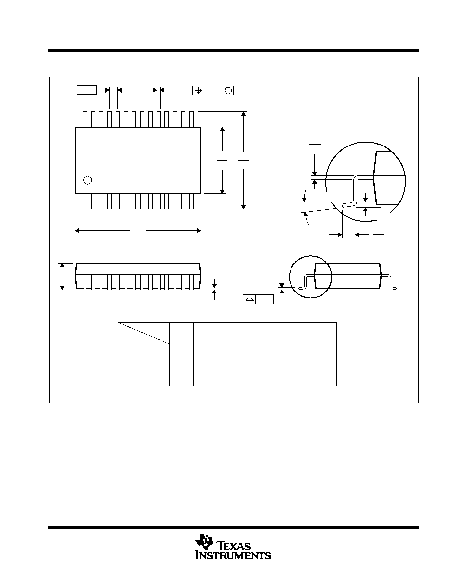
MECHANICAL DATA
MSSO002E � JANUARY 1995 � REVISED DECEMBER 2001
POST OFFICE BOX 655303
�
DALLAS, TEXAS 75265
DB (R-PDSO-G**)
PLASTIC SMALL-OUTLINE
4040065 /E 12/01
28 PINS SHOWN
Gage Plane
8,20
7,40
0,55
0,95
0,25
38
12,90
12,30
28
10,50
24
8,50
Seating Plane
9,90
7,90
30
10,50
9,90
0,38
5,60
5,00
15
0,22
14
A
28
1
20
16
6,50
6,50
14
0,05 MIN
5,90
5,90
DIM
A MAX
A MIN
PINS **
2,00 MAX
6,90
7,50
0,65
M
0,15
0
�
� 8
�
0,10
0,09
0,25
NOTES: A. All linear dimensions are in millimeters.
B. This drawing is subject to change without notice.
C. Body dimensions do not include mold flash or protrusion not to exceed 0,15.
D. Falls within JEDEC MO-150

IMPORTANT NOTICE
Texas Instruments Incorporated and its subsidiaries (TI) reserve the right to make corrections, modifications,
enhancements, improvements, and other changes to its products and services at any time and to discontinue
any product or service without notice. Customers should obtain the latest relevant information before placing
orders and should verify that such information is current and complete. All products are sold subject to TI's terms
and conditions of sale supplied at the time of order acknowledgment.
TI warrants performance of its hardware products to the specifications applicable at the time of sale in
accordance with TI's standard warranty. Testing and other quality control techniques are used to the extent TI
deems necessary to support this warranty. Except where mandated by government requirements, testing of all
parameters of each product is not necessarily performed.
TI assumes no liability for applications assistance or customer product design. Customers are responsible for
their products and applications using TI components. To minimize the risks associated with customer products
and applications, customers should provide adequate design and operating safeguards.
TI does not warrant or represent that any license, either express or implied, is granted under any TI patent right,
copyright, mask work right, or other TI intellectual property right relating to any combination, machine, or process
in which TI products or services are used. Information published by TI regarding third-party products or services
does not constitute a license from TI to use such products or services or a warranty or endorsement thereof.
Use of such information may require a license from a third party under the patents or other intellectual property
of the third party, or a license from TI under the patents or other intellectual property of TI.
Reproduction of information in TI data books or data sheets is permissible only if reproduction is without
alteration and is accompanied by all associated warranties, conditions, limitations, and notices. Reproduction
of this information with alteration is an unfair and deceptive business practice. TI is not responsible or liable for
such altered documentation.
Resale of TI products or services with statements different from or beyond the parameters stated by TI for that
product or service voids all express and any implied warranties for the associated TI product or service and
is an unfair and deceptive business practice. TI is not responsible or liable for any such statements.
Following are URLs where you can obtain information on other Texas Instruments products and application
solutions:
Products
Applications
Amplifiers
amplifier.ti.com
Audio
www.ti.com/audio
Data Converters
dataconverter.ti.com
Automotive
www.ti.com/automotive
DSP
dsp.ti.com
Broadband
www.ti.com/broadband
Interface
interface.ti.com
Digital Control
www.ti.com/digitalcontrol
Logic
logic.ti.com
Military
www.ti.com/military
Power Mgmt
power.ti.com
Optical Networking
www.ti.com/opticalnetwork
Microcontrollers
microcontroller.ti.com
Security
www.ti.com/security
Telephony
www.ti.com/telephony
Video & Imaging
www.ti.com/video
Wireless
www.ti.com/wireless
Mailing Address:
Texas Instruments
Post Office Box 655303 Dallas, Texas 75265
Copyright
2004, Texas Instruments Incorporated