 | –≠–ª–µ–∫—Ç—Ä–æ–Ω–Ω—ã–π –∫–æ–º–ø–æ–Ω–µ–Ω—Ç: PCM3002 | –°–∫–∞—á–∞—Ç—å:  PDF PDF  ZIP ZIP |
Æ
1
PCM3002/3003
PCM3002
PCM3003
Æ
PCM3002
PCM3003
FEATURES
q
MONOLITHIC 20-BIT
ADC AND DAC
q
16-/20-BIT
INPUT/OUTPUT DATA
q
SOFTWARE CONTROL: PCM3002
q
HARDWARE CONTROL: PCM3003
q
STEREO ADC:
Single-Ended Voltage Input
64 X Oversampling
High Performance
THD+N: ≠86dB
SNR: 90dB
Dynamic Range: 90dB
q
STEREO DAC:
Single-Ended Voltage Output
Analog Low Pass Filter
64X Oversampling
High Performance
THD+N: ≠86dB
SNR: 94dB
Dynamic Range: 94dB
q
SPECIAL FEATURES
Digital De-emphasis
Digital Attenuation (256 Steps)
Soft Mute
Digital Loop Back
Power Down: ADC/DAC Independent
q
SAMPLING RATE: Up to 48kHz
q
SYSTEM CLOCK: 256f
S
, 384f
S
, 512f
S
q
SINGLE +3V POWER SUPPLY
q
SMALL PACKAGE: SSOP-24
16-/20-Bit Single-Ended Analog Input /Output
STEREO AUDIO CODECs
TM
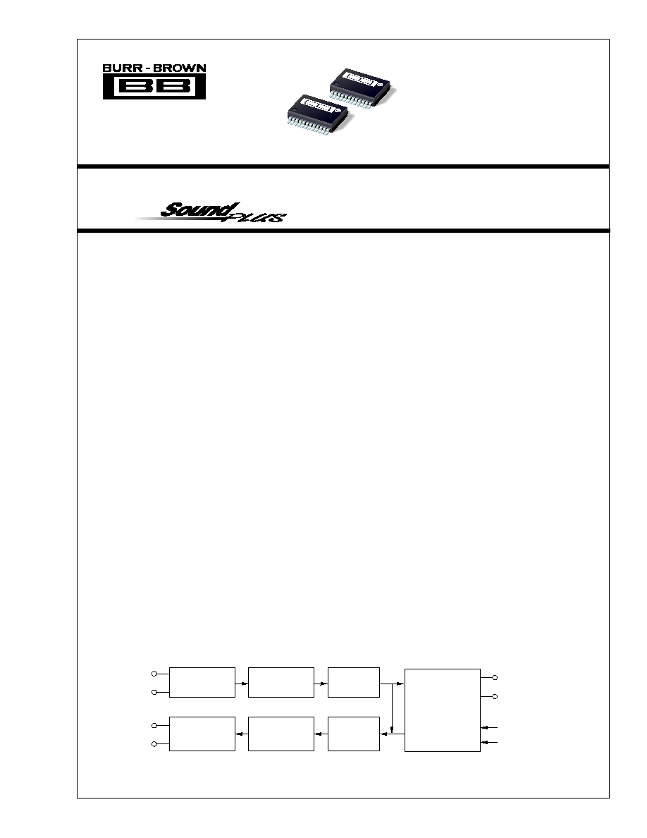
DESCRIPTION
The PCM3002 and PCM3003 are low cost single chip
stereo audio CODECs (analog-to-digital and digital-to-
analog converters) with single-ended analog voltage
input and output.
The ADCs and DACs employ delta-sigma modulation
with 64X oversampling. The ADCs include a digital
decimation filter, and the DACs include an 8X
oversampling digital interpolation filter. The DACs
also include digital attenuation, de-emphasis, infinite
zero detection and soft mute to form a complete
subsystem. PCM3002 and PCM3003 operate with
left-justified, and right-justified formats, while the
PCM3002 also supports the I
2
S data format.
PCM3002 and PCM3003 provide a power-down mode
that operates on the ADCs and DACs independently.
Fabricated on a highly advanced CMOS process,
PCM3002 and PCM3003 are suitable for a wide vari-
ety of cost-sensitive consumer applications where good
performance is required.
PCM3002's programmable functions are controlled
by software and the PCM3003's functions include de-
emphasis, power down, and audio data format selec-
tions, which are controlled by hardware.
© 1997 Burr-Brown Corporation
PDS-1414C
Printed in U.S.A. January, 2000
Lch In
Rch In
Analog Front-End
Delta-Sigma
Modulator
Digital
Decimation
Filter
Serial Interface
and
Mode Control
Digital Out
Digital In
Serial Mode Control
System Clock
Lch Out
Rch Out
Low Pass Filter
and
Output Buffer
Multi-Level
Delta-Sigma
Modulator
Digital
Interpolation
Filter
International Airport Industrial Park ∑ Mailing Address: PO Box 11400, Tucson, AZ 85734 ∑ Street Address: 6730 S. Tucson Blvd., Tucson, AZ 85706 ∑ Tel: (520) 746-1111
Twx: 910-952-1111 ∑ Internet: http://www.burr-brown.com/ ∑ Cable: BBRCORP ∑ Telex: 066-6491 ∑ FAX: (520) 889-1510 ∑ Immediate Product Info: (800) 548-6132
For most current data sheet and other product
information, visit www.burr-brown.com
SBAS079
Æ
PCM3002/3003
2
SPECIFICATIONS
All specifications at +25
∞
C, V
DD
= V
CC
= 3.0V, f
S
= 44.1kHz, SYSCLK = 384f
S
, and 16-bit data, unless otherwise noted.
The information provided herein is believed to be reliable; however, BURR-BROWN assumes no responsibility for inaccuracies or omissions. BURR-BROWN assumes no
responsibility for the use of this information, and all use of such information shall be entirely at the user's own risk. Prices and specifications are subject to change without notice.
No patent rights or licenses to any of the circuits described herein are implied or granted to any third party. BURR-BROWN does not authorize or warrant any BURR-BROWN
product for use in life support devices and/or systems.
NOTES: (1) Pins 7, 8, 17 and 18: RST, ML, MD, MC for the PCM3002; PDAD, PDDA, DEM1, DEM0 for PCM3003 (Schmitt-Trigger input with 100k
typical internal
pull-down resistor). (2) Pins 9, 10, 11, 15: SYSCLK, LRCIN, BCKIN, DIN (Schmitt Trigger input). (3) Pin16: 20BIT for PCM3003 (Schmitt-Trigger input, 100k
typical internal pull-down resistor). (4) Pin 12: DOUT. (5) Pin 16: ZFLG (open drain output). (6) High Pass Filter for Offset Cancel. (7) Refer to Application Bulletin
AB-148 for information relating to operation at lower sampling frequencies. (8) f
IN
= 1kHz, using Audio Precision System II, rms mode with 20kHz LPF, 400Hz
HPF used for performance calculation. (9) f
OUT
= 1kHz, using Audio Precision System II, r ms mode with 20kHz LPF, 400Hz HPF used for performance calculation.
(10) Applies for voltages between 2.4V to 2.7V for 0
∞
C to +70
∞
C and 256f
S
/512f
S
operation (384f
S
not available). (11) SYSCLK, BCKIN, and LRCIN are stopped.
PCM3002E/3003E
PARAMETER
CONDITIONS
MIN
TYP
MAX
UNITS
DIGITAL INPUT/OUTPUT
Input Logic
Input Logic Level: V
IH
(1, 2, 3)
0.7 x V
DD
VDC
V
IL
(1, 2, 3)
0.3 x V
DD
VDC
Input Logic Current: I
IN
(2)
±
1
µ
A
Input Logic Current: I
IN
(1)
100
µ
A
Output Logic
Output Logic Level: V
OH
(5)
I
OUT
= ≠1mA
V
DD
≠0.3
VDC
V
OL
(5)
I
OUT
= +1mA
0.3
VDC
Output Logic Level: V
OL
(4)
I
OUT
= +1mA
0.3
VDC
CLOCK FREQUENCY
Sampling Frequency (f
S
)
32
(7)
44.1
48
kHz
System Clock Frequency
256f
S
8.1920
11.2896
12.2880
MHz
384f
S
12.2880
16.9344
18.4320
MHz
512f
S
16.3840
22.5792
24.5760
MHz
ADC CHARACTERISTICS
RESOLUTION
20
Bits
DC ACCURACY
Gain Mismatch Channel-to-Channel
±
1.0
±
3.0
% of FSR
Gain Error
±
2.0
±
5.0
% of FSR
Gain Drift
±
20
ppm of FSR/
∞
C
Bipolar Zero Error
High-Pass Filter Disabled
(6)
±
1.7
% of FSR
Bipolar Zero Drift
High-Pass Filter Disabled
(6)
±
20
ppm of FSR/
∞
C
DYNAMIC PERFORMANCE
(8)
THD+N: V
IN
= ≠0.5dB
≠86
≠80
dB
V
IN
= ≠60dB
≠28
dB
Dynamic Range
A-Weighted
86
90
dB
Signal-to-Noise Ratio
A-Weighted
86
90
dB
Channel Separation
84
88
dB
DIGITAL FILTER PERFORMANCE
Passband
0.454f
S
Hz
Stopband
0.583f
S
Hz
Passband Ripple
±
0.05
dB
Stopband Attenuation
≠65
dB
Delay Time
17.4/f
S
sec
HPF Frequency Response
≠3dB
0.019f
S
mHz
ANALOG INPUT
Voltage Range
0.60 V
CC
Vp-p
Center Voltage
0.50 V
CC
V
Input Impedance
30
k
Anti-Aliasing Filter Frequency Response
≠3dB
150
kHz
Æ
3
PCM3002/3003
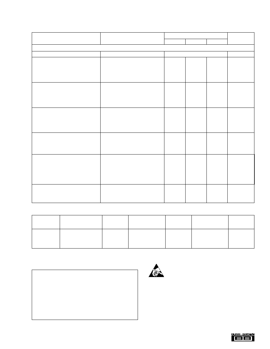
SPECIFICATIONS
All specifications at +25
∞
C, V
DD
= V
CC
= 3.0V, f
S
= 44.1kHz, SYSCLK = 384f
S
, CLKIO Input, 18-bit data, unless otherwise noted.
PCM3002E/3003E
PARAMETER
CONDITIONS
MIN
TYP
MAX
UNITS
Supply Voltage
+V
DD
, +V
CC
1, +V
CC
2 ...................................................................... +6.5V
Supply Voltage Differences ...............................................................
±
0.1V
GND Voltage Differences ..................................................................
±
0.1V
Digital Input Voltage ...................................................... ≠0.3 to V
DD
+ 0.3V
Analog Input Voltage ......................................... ≠0.3 to V
CC
1,
V
CC
2 + 0.3V
Power Dissipation .......................................................................... 300mW
Input Current ...................................................................................
±
10mA
Operating Temperature Range ......................................... ≠25
∞
C to +85
∞
C
Storage Temperature ...................................................... ≠55
∞
C to +125
∞
C
Lead Temperature (soldering, 5s) .................................................. +260
∞
C
(reflow, 10s) ..................................................... +235
∞
C
ABSOLUTE MAXIMUM RATINGS
ELECTROSTATIC
DISCHARGE SENSITIVITY
This integrated circuit can be damaged by ESD. Burr-Brown
recommends that all integrated circuits be handled with
appropriate precautions. Failure to observe proper handling
and installation procedures can cause damage.
ESD damage can range from subtle performance degrada-
tion to complete device failure. Precision integrated circuits
may be more susceptible to damage because very small
parametric changes could cause the device not to meet its
published specifications.
DAC CHARACTERISTICS
RESOLUTION
20
Bits
DC ACCURACY
Gain Mismatch Channel-to-Channel
±
1.0
±
3
% of FSR
Gain Error
±
1.0
±
5
% of FSR
Gain Drift
±
20
ppm of FSR/
∞
C
Bipolar Zero Error
±
1.0
% of FSR
Bipolar Zero Drift
±
20
ppm of FSR/
∞
C
DYNAMIC PERFORMANCE
(9)
THD+N: V
OUT
= 0dB (Full Scale)
≠86
≠80
dB
V
OUT
= ≠60dB
≠28
dB
Dynamic Range
EIAJ, A-Weighted
88
94
dB
Signal-to-Noise Ratio
EIAJ, A-Weighted
88
94
dB
Channel Separation
86
91
dB
DIGITAL FILTER PERFORMANCE
Passband
0.445f
S
Hz
Stopband
0.555f
S
Hz
Passband Ripple
±
0.17
dB
Stopband Attenuation
≠35
dB
Delay Time
11.1/f
S
sec
ANALOG OUTPUT
Voltage Range
0.60 x V
CC
Vp-p
Center Voltage
0.5 x V
CC
VDC
Load Impedance
AC-Coupling
10
k
LPF Frequency Response
f = 20kHz
≠0.16
dB
POWER SUPPLY REQUIREMENTS
Voltage Range: V
CC
, V
DD
≠25
∞
C to +85
∞
C
2.7
3.0
3.6
VDC
0
∞
C to +70
∞
C
(10)
2.4
3.0
3.6
VDC
Supply Current: Operation
V
CC
= V
DD
= 3.0V
18
24
mA
Power-Down
V
CC
= V
DD
= 3.0V
50
µ
A
Power Dissipation: Operation
V
CC
= V
DD
= 3.0V
54
72
mW
Power-Down
(11)
V
CC
= V
DD
= 3.0V
150
µ
W
TEMPERATURE RANGE
Operation
≠25
+85
∞
C
Storage
≠55
+125
∞
C
Thermal Resistance,
JA
100
∞
C/W
PACKAGE
SPECIFIED
DRAWING
TEMPERATURE
PACKAGE
ORDERING
TRANSPORT
PRODUCT
PACKAGE
NUMBER
RANGE
MARKING
NUMBER
(1)
MEDIA
PCM3002E
SSOP-24
338
≠25
∞
C to +85
∞
C
PCM3002E
PCM3002E
Rails
"
"
"
"
"
PCM3002E/2K
Tape and Reel
PCM3003E
SSOP-24
338
≠25
∞
C to +85
∞
C
PCM3003E
PCM3003E
Rails
"
"
"
"
"
PCM3003E/2K
Tape and Reel
NOTES: (1) Models with a slash (/) are available only in Tape and Reel in the quantities indicated (e.g., /2K indicates 2000 devices per reel). Ordering 2000 pieces
of "PCM3002E/2K" will get a single 2000-piece Tape and Reel.
PACKAGE/ORDERING INFORMATION
Æ
PCM3002/3003
4
V
CC
1
V
CC
1
V
IN
R
V
REF
L
V
REF
R
V
IN
L
PDAD
PDDA
SYSCLK
LRCIN
BCKIN
DOUT
V
CC
2
AGND1
AGND2
V
COM
V
OUT
R
V
OUT
L
DEM0
DEM1
20BIT
DIN
V
DD
DGND
1
2
3
4
5
6
7
8
9
10
11
12
24
23
22
21
20
19
18
17
16
15
14
13
PCM3003
V
CC
1
V
CC
1
V
IN
R
V
REF
L
V
REF
R
V
IN
L
RST
ML
SYSCLK
LRCIN
BCKIN
DOUT
V
CC
2
AGND1
AGND2
V
COM
V
OUT
R
V
OUT
L
MC
MD
ZFLG
DIN
V
DD
DGND
1
2
3
4
5
6
7
8
9
10
11
12
24
23
22
21
20
19
18
17
16
15
14
13
PCM3002
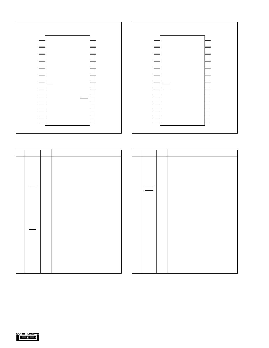
PIN CONFIGURATION--PCM3002
PIN CONFIGURATION--PCM3003
Top View
SSOP
Top View
SSOP
PIN
NAME
I/O
DESCRIPTION
1
V
CC
1
--
ADC Analog Power Supply
2
V
CC
1
--
ADC Analog Power Supply
3
V
IN
R
IN
ADC Analog Input, Rch
4
V
REF
L
--
ADC Reference, Lch
5
V
REF
R
--
ADC Reference, Rch
6
V
IN
L
IN
ADC Analog Input, Lch
7
RST
IN
Reset, Active LOW
(1, 2)
8
ML
IN
Strobe Pulse for Mode Control
(1, 2)
9
SYSCLK
IN
System Clock Input
(2)
10
LRCIN
IN
Sample Rate Clock Input (f
S
)
(2)
11
BCKIN
IN
Bit Clock Input
(2)
12
DOUT
OUT
Data Output
13
DGND
--
Digital Ground
14
V
DD
--
Digital Power Supply
15
DIN
IN
Data Input
(2)
16
ZFLG
OUT
Zero Flag Output, Active LOW
(3)
17
MD
IN
Serial Data for Mode Control
(1, 2)
18
MC
IN
Bit Clock for Mode Control
(1, 2)
19
V
OUT
L
OUT
DAC Analog Output, Lch
20
V
OUT
R
OUT
DAC Analog Output, Rch
21
V
COM
--
ADC/DAC Common
22
AGND2
--
DAC Analog Ground
23
AGND1
--
ADC Analog Ground
24
V
CC
2
--
DAC Analog Power Supply
NOTES: (1) With 100k
typical internal pull-down resistor. (2) Schmitt-Trigger
input. (3) Open drain output.
PIN ASSIGNMENTS--PCM3002
PIN
NAME
I/O
DESCRIPTION
1
V
CC
1
--
ADC Analog Power Supply
2
V
CC
1
--
ADC Analog Power Supply
3
V
IN
R
IN
ADC Analog Input, Rch
4
V
REF
L
--
ADC Reference, Lch
5
V
REF
R
--
ADC Reference, Rch
6
V
IN
L
IN
ADC Analog Input, Lch
7
PDAD
IN
ADC Power Down, Active LOW
(1, 2)
8
PDDA
IN
DAC Power Down, Active LOW
(1, 2)
9
SYSCLK
IN
System Clock Input
(2)
10
LRCIN
IN
Sample Rate Clock Input (f
S
)
(2)
11
BCKIN
IN
Bit Clock Input
(2)
12
DOUT
OUT
Data Output
13
DGND
--
Digital Ground
14
V
DD
--
Digital Power Supply
15
DIN
IN
Data Input
16
20BIT
IN
20-Bit Format Select
(1, 2)
17
DEM1
IN
De-emphasis Control
(1, 2)
18
DEM0
IN
De-emphasis Control 0
(1, 2)
19
V
OUT
L
OUT
DAC Analog Output, Lch
20
V
OUT
R
OUT
DAC Analog Output, Rch
21
V
COM
--
ADC/DAC Common
22
AGND2
--
DAC Analog Ground
23
AGND1
--
ADC Analog Ground
24
V
CC
2
--
DAC Analog Power Supply
NOTE: (1) With 100k
typical internal pull-down resistor. (2) Schmitt-Trigger
input.
PIN ASSIGNMENTS--PCM3003
Æ
5
PCM3002/3003
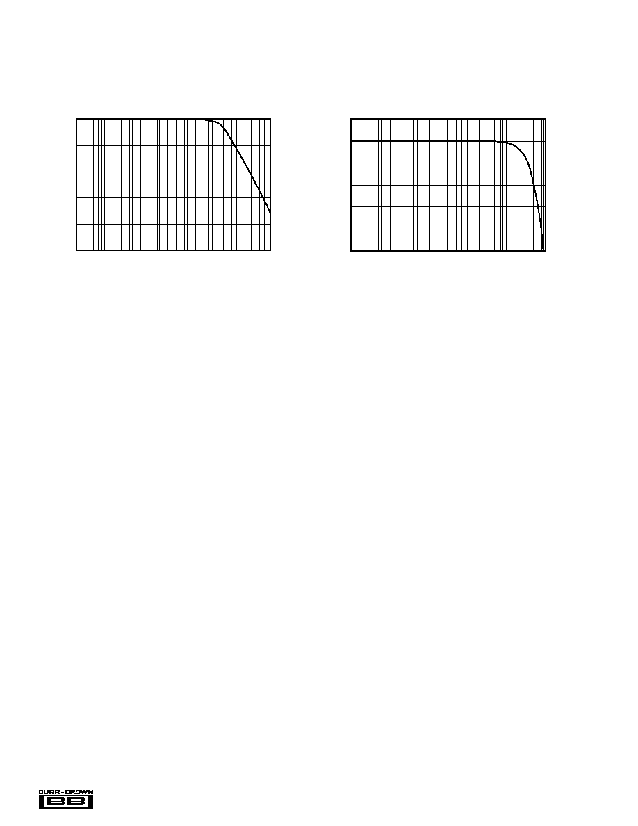
TYPICAL PERFORMANCE CURVES
ADC SECTION
At T
A
= +25
∞
C, V
CC
= V
DD
= 3.0V, f
S
= 44.1kHz, f
SYSCLK
= 384f
S
, and F
SIGNAL
= 1kHz, unless otherwise noted.
THD+N vs TEMPERATURE
Temperature (∞C)
THD+N at ≠0.5dB (%)
0.010
0.008
0.006
0.004
0.002
≠25
0
25
50
75
85
100
THD+N at ≠60dB (%)
5.0
4.0
2.0
3.0
1.0
≠60dB
0.5dB
DYNAMIC RANGE and SNR vs TEMPERATURE
Temperature (∞C)
Dynamic Range (dB)
94
92
90
88
86
≠25
0
25
50
75
85
100
SNR (dB)
5.0
4.0
2.0
3.0
1.0
SNR
Dynamic Range
DYNAMIC RANGE and SNR vs SUPPLY VOLTAGE
Supply Voltage
(V)
Dynamic Range (dB)
94
92
90
88
86
2.4
2.7
3.0
3.3
3.6
SNR (dB)
94
92
90
88
86
Dynamic Range
SNR
THD+N vs SUPPLY VOLTAGE
Supply Voltage
(V)
THD+N at ≠0.50dB (%)
0.010
0.008
0.006
0.004
0.002
2.4
2.7
3.0
3.3
3.6
THD+N at ≠60dB (%)
5.0
4.0
3.0
2.0
1.0
≠60dB
≠0.5dB
THD+N vs SAMPLING FREQUENCY
f
S
(kHz)
THD+N at ≠0.5dB (%)
0.010
0.008
0.006
0.004
0.002
32
44.1
48
THD+N at ≠60dB (%)
5.0
4.0
3.0
2.0
1.0
≠60dB
≠0.5dB
DYNAMIC RANGE and SNR vs SAMPLING FREQUENCY
f
S
(kHz)
Dynamic Range (dB)
94
92
90
88
86
32
44.1
48
SNR (dB)
94
92
90
88
86
Dynamic Range
SNR
Æ
PCM3002/3003
6
TYPICAL PERFORMANCE CURVES
DAC SECTION
At T
A
= +25
∞
C, V
CC
= V
DD
= 3.0V, f
S
= 44.1kHz, f
SYSCLK
= 384f
S
, and F
SIGNAL
= 1kHz, unless otherwise noted.
DYNAMIC RANGE and SNR vs TEMPERATURE
Temperature (∞C)
Dynamic Range (dB)
98
96
94
92
90
≠25
0
25
50
75
85
100
SNR (dB)
98
96
94
92
90
SNR
Dynamic Range
DYNAMIC RANGE and SNR vs SUPPLY VOLTAGE
Supply Voltage
(V)
Dynamic Range (dB)
98
96
94
92
90
2.4
2.7
3.0
3.3
3.6
SNR (dB)
98
96
94
92
90
SNR
Dynamic Range
DYNAMIC RANGE and SNR
vs SAMPLING FREQUENCY and SYSTEM CLOCK
f
S
(kHz)
Dynamic Range (dB)
98
96
94
92
90
32
44.1
48
SNR (dB)
98
96
94
92
90
SNR
Dynamic
Range
384f
S
256f
S
, 512f
S
THD+N vs TEMPERATURE
Temperature (
∞
C)
THD+N at FS (%)
0.010
0.008
0.006
0.004
0.002
≠25
0
25
50
75
85
100
THD+N at ≠60dB (%)
4.0
3.0
2.0
1.0
0
0dB
≠60dB
THD+N vs SUPPLY VOLTAGE
Supply Voltage
(V)
THD+N at FS (%)
0.010
0.008
0.006
0.004
0.002
2.4
2.7
3.0
3.3
3.6
THD+N at ≠60dB (%)
4.0
3.0
2.0
1.0
0
≠60dB
0dB
THD+N vs SAMPLING FREQUENCY
and SYSTEM CLOCK
f
S
(kHz)
THD+N at FS (%)
0.010
0.008
0.006
0.004
0.002
32
44.1
48
THD+N at ≠60dB (%)
4.0
3.0
2.0
1.0
0
≠60dB
384f
S
256f
S
, 512f
S
384f
S
256f
S
, 512f
S
0dB
Æ
7
PCM3002/3003
OUTPUT SPECTRUM (0dB, N = 8192)
Frequency (kHz)
Amplitude (dB)
0
≠20
≠40
≠60
≠80
≠100
≠120
≠140
5
10
15
25
22
20
0
OUTPUT SPECTRUM (≠60dB, N = 8192)
Frequency (kHz)
Amplitude (dB)
0
≠20
≠40
≠60
≠80
≠100
≠120
≠140
5
10
15
25
20
22
0
OUTPUT SPECTRUM (≠60dB, N = 8192)
Frequency (kHz)
Amplitude (dB)
0
≠20
≠40
≠60
≠80
≠100
≠120
≠140
5
10
15
25
20 22
0
TYPICAL PERFORMANCE CURVES
Output Spectrum
At T
A
= +25
∞
C, V
CC
= V
DD
= 3.0V, f
S
= 44.1kHz, f
SYSCLK
= 384f
S
, and F
SIGNAL
= 1kHz, unless otherwise noted.
DACs
ADCs
THD+N vs SIGNAL LEVEL
Signal Level (dB)
THD+N (%)
100
10
1
0.1
0.001
0.001
≠72
≠84
≠96
≠60
≠48
≠36
≠12
≠24
0
THD+N vs SIGNAL LEVEL
Signal Level (dB)
THD+N (%)
100
10
1
0.1
0.001
0.001
≠72
≠84
≠96
≠60
≠48
≠36
≠12
≠24
0
OUTPUT SPECTRUM (0dB, N = 8192)
Frequency (kHz)
Amplitude (dB)
0
≠20
≠40
≠60
≠80
≠100
≠120
≠140
5
10
15
25
22
20
0

Æ
PCM3002/3003
8
I
CC
+ I
DD
vs SAMPLING FREQUENCY
f
S
(kHz)
I
CC
+ I
DD
(mA)
20
19
18
17
16
15
32
44.1
48
ADC & DAC
512f
S
256f
S
TYPICAL PERFORMANCE CURVES
Supply Current
At T
A
= +25
∞
C, V
CC
= V
DD
= 3.0V, f
S
= 44.1kHz, f
SYSCLK
= 384f
S
, DIN = BPZ, and V
IN
= BPZ, unless otherwise noted.
I
CC
+ I
DD
vs TEMPERATURE
Temperature (∞C)
I
CC
+ I
DD
(mA)
I
CC
+ I
DD:
Power Down and OFF (mA)
25
20
15
10
5
0
2.5
2.0
1.5
1.0
0.5
0
≠25
≠50
≠0
25
50
75
100
ADC
DAC
Power Down & OFF
ADC & DAC
I
CC
+ I
DD
vs SUPPLY VOLTAGE
Supply Voltage (V)
I
CC
+ I
DD
(mA)
I
CC
+ I
DD:
Power Down and OFF (mA)
25
20
15
10
5
0
2.5
2.0
1.5
1.0
0.5
0
2.4
2.7
3.0
3.3
3.6
Power Down & OFF
ADC & DAC
ADC
DAC
Æ
9
PCM3002/3003
TYPICAL PERFORMANCE CURVES
At T
A
= +25
∞
C, V
CC
= V
DD
= 3.0V, f
S
= 44.1kHz, and f
SYSCLK
= 384f
S
, unless otherwise noted.
ADC DIGITAL FILTER
OVERALL CHARACTERISTICS
Normalized Frequency (x f
S
Hz)
Amplitude (dB)
0
≠50
≠100
≠150
≠200
8
16
24
32
0
STOPBAND ATTENUATION CHARACTERISTICS
Normalized Frequency (x f
S
Hz)
Amplitude (dB)
0
≠10
≠20
≠30
≠40
≠50
≠60
≠70
≠80
≠90
≠100
0.2
0.4
0.6
0.8
1.0
0
PASSBAND RIPPLE CHARACTERISTICS
Normalized Frequency (x f
S
Hz)
Amplitude (dB)
0.2
0.0
≠0.2
≠0.4
≠0.6
≠0.8
≠1.0
0.1
0.2
0.3
0.4
0.5
0
HIGH PASS FILTER RESPONSE
Normalized Frequency (x f
S
/1000 Hz)
Amplitude (dB)
0
≠10
≠20
≠30
≠40
≠50
≠60
≠70
≠80
≠90
≠100
0.1
0.2
0.3
0.4
0.5
0
HIGH PASS FILTER RESPONSE
Normalized Frequency (x f
S
/1000 Hz)
Amplitude (dB)
0.2
0.0
≠0.2
≠0.4
≠0.6
≠0.8
≠1.0
1
2
3
4
0
TRANSITION BAND CHARACTERISTICS
Normalized Frequency (x f
S
Hz)
Amplitude (dB)
0
≠1
≠2
≠3
≠4
≠5
≠6
≠7
≠8
≠9
≠10
0.45
0.46 0.47 0.48 0.49
0.50 0.51
0.52 0.53 0.54 0.55
≠4.13dB at 0.5 x f
S
Æ
PCM3002/3003
10
TYPICAL PERFORMANCE CURVES
At T
A
= +25
∞
C, V
CC
= V
DD
= 3.0V, f
S
= 44.1kHz, and f
SYSCLK
= 384f
S
, unless otherwise noted.
ANTI-ALIASING FILTER
ANTI-ALIASING FILTER OVERALL
FREQUENCY RESPONSE
Frequency (Hz)
Amplitude (dB)
0
≠10
≠20
≠30
≠40
≠50
10
100
1k
10k
100k
1M
10M
0
ANTI-ALIASING FILTER PASSBAND
FREQUENCY RESPONSE
Frequency (Hz)
Amplitude (dB)
0.2
0.0
≠0.2
≠0.4
≠0.6
≠0.8
≠1.0
10
100
1k
10k
100k
0
Æ
11
PCM3002/3003
DE-EMPHASIS ERROR (32kHz)
0
3628
7256
10884
14512
0
4999.8375
9999.675
14999.5125
19999.35
0
5442
10884
16326
21768
Frequency (Hz)
0.6
0.4
0.2
0
≠0.2
≠0.4
≠0.6
0.6
0.4
0.2
0
≠0.2
≠0.4
≠0.6
0.6
0.4
0.2
0
≠0.2
≠0.4
≠0.6
DE-EMPHASIS ERROR (44.1kHz)
Frequency (Hz)
DE-EMPHASIS ERROR (48kHz)
Frequency (Hz)
Error (dB)
Error (dB)
Error (dB)
DE-EMPHASIS FREQUENCY RESPONSE (32kHz)
0
5k
10k
15k
20k
25k
Frequency (Hz)
0
≠2
≠4
≠6
≠8
≠10
≠12
DE-EMPHASIS FREQUENCY RESPONSE (44.1kHz)
0
5k
10k
15k
20k
25k
Frequency (Hz)
0
≠2
≠4
≠6
≠8
≠10
≠12
DE-EMPHASIS FREQUENCY RESPONSE (48kHz)
0
5k
10k
15k
20k
25k
Frequency (Hz)
0
≠2
≠4
≠6
≠8
≠10
≠12
Level (dB)
Level (dB)
Level (dB)
TYPICAL PERFORMANCE CURVES
At T
A
= +25
∞
C, V
CC
= V
DD
= 3.0V, f
S
= 44.1kHz, and f
SYSCLK
= 384f
S
, unless otherwise noted.
DAC DIGITAL FILTER
20
0
≠20
≠40
≠60
≠80
≠100
10
100
1k
10k
100k
1M
10M
Frequency (Hz)
Level (dB)
INTERNAL ANALOG FILTER FREQUENCY RESPONSE
(10Hz~10MHz)
0
50k
100k
150k
0
≠20
≠40
≠60
≠80
≠100
Level (dB)
OVERALL FREQUENCY CHARACTERISTICS
(f
S
= 44.1kHz)
Frequency (Hz)
PASSBAND RIPPLE CHARACTERISTICS (f
S
= 44.1kHz)
0
≠0.2
≠0.4
≠0.6
≠0.8
≠1.0
0
5k
10k
15k
20k
Level (dB)
Frequency (Hz)
0.15
0.10
0.05
0
≠0.05
≠0.10
≠0.15
Level (dB)
1
Frequency (Hz)
10
100
1k
10k
100k
INTERNAL ANALOG FILTER FREQUENCY RESPONSE
(1Hz~20kHz)
Æ
PCM3002/3003
12
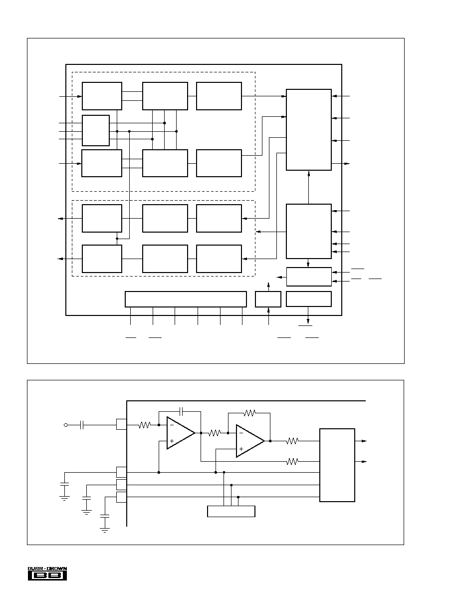
BLOCK DIAGRAM
FIGURE 1. Analog Front-End (Single-Channel).
30k
V
IN
R
1
21
4
5
V
COM
V
REF
L
V
REF
R
Delta-Sigma
Modulator
(+)
(≠)
V
REF
+
+
1.0µF
4.7µF
+
4.7µF
+
4.7µF
Interpolation
Filter
8X Oversampling
Interpolation
Filter
8X Oversampling
Multi-Level
Delta-Sigma
Modulator
Multi-Level
Delta-Sigma
Modulator
Clock
Reset and
Power Down
Zero Detect
(1)
RST
(1)
/PDAD
(2)
SYSCLK
ZFLG
(1)
AGND2
V
CC
2
AGND1
V
CC
1
PDDA
(2)
Reference
Mode
Control
Interface
ML
(1 )
20BIT
(2)
MC
(1 )
/DEM0
(2)
MD
(1 )
/DEM1
(2)
Serial Data
Interface
DOUT
BCKIN
LRCIN
DIN
V
IN
L
V
REF
L
V
COM
V
REF
R
V
IN
R
V
OUT
L
V
OUT
R
Power Supply
DGND
V
DD
Analog
Low-Pass
Filter
Analog
Low-Pass
Filter
Decimation
and
High Pass Filter
Delta-Sigma
Modulator
(≠)
(+)
Analog
Front-End
Circuit
Decimation
and
High Pass Filter
Delta-Sigma
Modulator
ADC
DAC
(+)
(≠)
Analog
Front-End
Circuit
NOTES: (1) MC, MD, ML, RST, and ZFLG are for PCM3002 only. (2) DEM0, DEM1, 20BIT, PDAD, and PDDA are for PCM3003 only.
Æ
13
PCM3002/3003
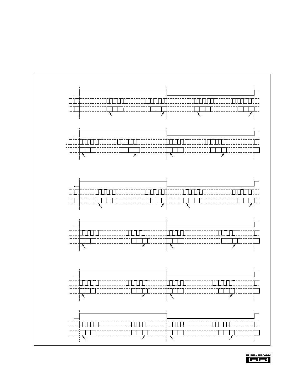
PCM AUDIO INTERFACE
The four-wire digital audio interface for PCM3002/3003 is
comprised of: LRCIN (pin 10), BCKIN (pin 11), DIN (pin
15), and DOUT (pin 12). The PCM3002 may be used with
any of the four input/output data formats (Formats 0 - 3),
while the PCM3003 may only be used with selected input/
output formats (Formats 0 - 1). For the PCM3002, these
formats are selected through PROGRAM REGISTER 3 in
the software mode. For the PCM3003, data formats are
selected by the 20BIT input (pin 16). Figures 2, 3 and 4
illustrate audio data input/output formats and timing.
The PCM3002/3003 can accept 32-, 48-, or 64-bit clocks
(BCKIN) in one clock of LRCIN. Only 16-bit data formats
can be selected when 32-bit clocks/LRCIN are applied.
FIGURE 2. Audio Data Input/Output Format.
MSB
L≠ch
R≠ch
L≠ch
R≠ch
LSB
LRCIN
BCKIN
FORMAT 0: PCM3002/3003
DIN
MSB
LSB
DAC: 16-Bit, MSB-First, Right-Justified
ADC: 16-Bit, MSB-First, Left-Justified
1
16
2
3
14 15 16
1
2
3
14 15 16
MSB
LSB
LRCIN
BCKIN
DOUT
MSB
LSB
1
2
3
14 15 16
1
2
3
14 15 16
1
MSB
L≠ch
R≠ch
L≠ch
R≠ch
LSB
LRCIN
BCIN
FORMAT 2: PCM3002 Only
DIN
MSB
LSB
DAC: 20-Bit, MSB-First, Left-Justified
ADC: 20-Bit, MSB-First, Left-Justified
1
2
3
18 19 20
1
2
3
18 19 20
MSB
LSB
LRCIN
BCIN
DOUT
MSB
LSB
1
2
3
18 19 20
1
2
3
18 19 20
MSB
L≠ch
R≠ch
L≠ch
R≠ch
LSB
LRCIN
BCKIN
FORMAT 1: PCM3002/3003
DIN
MSB
LSB
DAC: 20-Bit, MSB-First, Right-Justified
ADC: 20-Bit, MSB-First, Left-Justified
1
20
2
3
18 19 20
1
2
3
18 19 20
MSB
LSB
LRCIN
BCKIN
DOUT
MSB
LSB
1
2
3
18 19 20
1
2
3
18 19 20
1
1
1

Æ
PCM3002/3003
14
FIGURE 3. Audio Data Input/Output Format.
FIGURE 4. Audio Data Input/Output Timing.
BCKIN Pulse Cycle Time
t
BCY
300ns (min)
BCKIN Pulse Width High
t
BCH
120ns (min)
BCKIN Pulse Width Low
t
BCL
120ns (min)
BCKIN Rising Edge to LRCIN Edge
t
BL
40ns (min)
LRCIN Edge to BCKIN Rising Edge
t
LB
40ns (min)
LRCIN Pulse Width
t
LRP
t
BCY
(min)
DIN Set-up Time
t
DIS
40ns (min)
DIN Hold Time
t
DIH
40ns (min)
DOUT Delay Time to BCKIN Falling Edge
t
BDO
40ns (max)
DOUT Delay Time to LRCIN Edge
t
LDO
40ns (max)
Rising Time of All Signals
t
RISE
20ns (max)
Falling Time of All Signals
t
FALL
20ns (max)
t
BCH
t
BCY
t
BCL
t
LB
t
DIH
t
DIS
t
LRP
t
BL
t
LDO
t
BDO
BCKIN
LRCIN
DIN
DOUT
0.5V
DD
0.5V
DD
0.5V
DD
0.5V
DD
MSB
L-ch
R-ch
L-ch
R-ch
LSB
LRCIN
BCKIN
FORMAT 3: PCM3002 Only
DIN
MSB
LSB
DAC: 20-Bit, MSB-First, I
2
S
ADC: 20-Bit, MSB-First, I
2
S
1
2
3
18 19 20
1
2
3
18 19 20
MSB
LSB
LRCIN
BCKIN
DOUT
MSB
LSB
1
2
3
18 19 20
1
2
3
18 19 20

Æ
15
PCM3002/3003
SYSTEM CLOCK
The system clock for PCM3002/3003 must be either 256f
S
,
384f
S
or 512f
S
, where f
S
is the audio sampling frequency. The
system clock should be provided at the SYSCLK input (pin 9).
The PCM3002/3003 also has a system clock detection circuit
which automatically senses if the system clock is operating at
256f
S
, 384f
S
, or 512f
S
. When 384f
S
or 512f
S
system clock is
used, the clock is divided into 256f
S
automatically. The 256f
S
clock is used to operate the digital filters and the delta-sigma
modulators.
Table I lists the relationship of typical sampling frequencies
and system clock frequencies, while Figure 5 illustrates the
system clock timing.
POWER-ON RESET
Both the PCM3002 and PCM3003 have internal power-on
reset circuitry. Power-on reset occurs when system clock
(SYSCLK) is active and V
DD
> 2.2V. For the PCM3003, the
SYSCLK must complete a minimum of 3 complete cycles
prior to V
DD
> 2.2V to ensure proper reset operation. The
initialization sequence requires 1024 SYSCLK cycles for
completion, as shown in Figure 6. Figure 8 shows the state
of the DAC and ADC outputs during and after the reset
sequence.
EXTERNAL RESET
The PCM3002 includes a reset input, RST (pin 7), while the
PCM3003 utilizes both PDAD (pin 7) and PDDA (pin 8) for
external reset control. As shown in Figure 7, the external
reset signal must drive RST or PDAD/PDDA low for a
minimum of 40 nanoseconds while SYSCLK is active in
order to initiate the reset sequence. Initialization starts on the
rising edge of RST or PDAD/PDDA, and requires 1024
SYSCLK cycles for completion. Figure 8 shows the state of
the DAC and ADC outputs during and after the reset se-
quence.
SAMPLING RATE FREQUENCY
SYSTEM CLOCK FREQUENCY
(kHz)
(MHz)
256f
S
384f
S
512f
S
32
8.1920
12.2880
16.3840
44.1
11.2896
16.9340
22.5792
48
12.2880
18.4320
24.5760
TABLE I. System Clock Frequencies.
System Clock Pulse Width High
t
SCKH
12ns
(min)
System Clock Pulse Width Low
t
SCKL
12ns
(min)
t
SCKH
t
SCKL
1/256f
S
,1/384f
S
,or 1/512f
S
0.7V
"H"
SYSCLK
"L"
0.3V
DD
FIGURE 5. System Clock Timing.
1024 System Clock Periods
Reset
Reset Removal
2.4V
2.2V
2.0V
V
DD
Internal Reset
SYSCLK
FIGURE 6. Internal Power-On Reset Timing.
1024 System Clock Periods
Reset
Reset Removal
SYSCLK
Internal Reset
RST
or
PDAD and PDDA
t
RST
t
RST
= 40ns minimum
FIGURE 7. External Forced Reset Timing.
Æ
PCM3002/3003
16
synchronization occurs followed by t
ADCDLY2
delay time. If
LRCIN is synchronized with 5 or less bit clocks to the system
clock, operation will be normal. Figure 9 illustrates the effects
on the output when synchronization is lost. Before the outputs
are forced to bipolar zero (<1/f
S
seconds), the outputs are not
defined and some noise may occur. During the transitions
between normal data and undefined states, the output has
discontinuities, which will cause output noise.
ZERO FLAG OUTPUT: PCM3002 ONLY
Pin 16 is an open-drain output, used as the infinite zero
detection flag on the PCM3002 only. When input data is
continuously zero for 65,536 BCKIN cycles, ZFLG is LOW,
otherwise, ZFLG is in a high-impedance state.
Synchronous
Asynchronous
Synchronization
Lost
Resynchronization
within
1/f
S
Synchronous
Normal
Normal
t
ADCDLY2
(32/f
S
)
t
DACDLY2
(32/f
S
)
Undefined Data
V
COM
(= 1/2 x V
CC
)
Undefined Data
State of
Synchronization
DAC V
OUT
Normal
Normal
(1 )
Zero
ADC DOUT
NOTES: (1) The HPF transient response (exponentially attenuated signal from ±0.2% DC of FSR
with 200ms time constant) appears initially.
Reset
Power Down
GND
V
COM
(0.5V
CC
)
Ready/Operation
Internal Reset
or Power Down
ADC DOUT
DAC V
OUT
Zero
Zero
Normal Data
(1)
t
ADCDLY1
(18436/f
S
)
t
DACDLY1
(16384/f
S
)
Reset Removal or Power Down OFF
NOTE: (1) The HPF transient response (exponentially attenuated signal from ±0.2% DC of FSR
with 200ms time constant) appears initially.
SYNCHRONIZATION WITH THE DIGITAL
AUDIO SYSTEM
The PCM3002/3003 operates with LRCIN synchronized to
the system clock. PCM3002/3003 does not require any spe-
cific phase relationship between LRCIN and the system
clock, but there must be synchronization. If the synchroniza-
tion between the system clock and LRCIN changes more than
6 bit clocks (BCKIN) during one sample (LRCIN) period
because of phase jitter on LRCIN, internal operation of the
DAC will stop within 1/f
S
, and the analog output will be
forced to bipolar zero (0.5V
CC
) until the system clock is re-
synchronized to LRCIN followed by t
DACDLY2
delay time.
Internal operation of the ADC will also stop within 1/f
S
, and
the digital output codes will be set to bipolar zero until re-
FIGURE 8. DAC Output and ADC Output for Reset and Power Down.
FIGURE 9. DAC Output and ADC Output for Loss of Synchronization.

Æ
17
PCM3002/3003
B15 B14 B13 B12 B11 B10 B9 B8 B7 B6 B5 B4 B3 B2 B1 B0
ML
MC
MD
FIGURE 10. Control Data Input Format.
MC Pulse Cycle Time
t
MCY
100ns (min)
MC Pulse Width LOW
t
MCL
40ns (min)
MC Pulse Width HIGH
t
MCH
40ns (min)
MD Setup Time
t
MDS
40ns (min)
MD Hold Time
t
MDH
40ns (min)
ML Low Level Time
t
MLL
40ns + 1SYSCLK (min)
ML High Level Time
t
MLH
40ns + 1SYSCLK (min)
ML Setup Time
t
MLS
40ns (min)
ML Hold Time
t
MLH
40ns (min)
SYSCLK: 1/256f
S
or 1/384f
S
or 1/512f
S
ML
MC
MD
t
MLL
t
MLH
t
MCH
t
MCL
t
MDS
t
MCY
t
MLS
t
MLH
t
MDH
LSB
FIGURE 11. Control Data Input Timing.
FUNCTION
ADC/DAC
PCM3002
PCM3003
Audio Data Format
ADC/DAC
4 Selectable Formats
2 Selectable Formats
LRCIN Polarity
ADC/DAC
O
X
Loop-Back Control
ADC/DAC
O
X
Left Channel Attenuation
DAC
O
X
Right Channel Attenuation
DAC
O
X
Attenuation Control
DAC
O
X
Infinite Zero Detection
DAC
O
X
DAC Output Control
DAC
O
X
Soft Mute Control
DAC
O
X
De-Emphasis (OFF, 32kHz, 44.1kHz, 48kHz)
DAC
O
O
ADC Power-Down Control
ADC
O
O
DAC Power-Down Control
DAC
O
O
High Pass Filter Operation
ADC
O
X
TABLE II. Selectable Functions (O = User Selectable; X = Not Available).
OPERATIONAL CONTROL
PCM3002 can be controlled in a software mode with a
three-wire serial interface on MC (pin 18), MD (pin 17), and
ML (pin 8). Table II indicates selectable functions, and
Figure 10 and 11 illustrate the control data input format and
timing. PCM3003 only allows for control of 16-/20-bit data
format, digital de-emphasis, and Power-Down Control by
hardware pins.
Æ
PCM3002/3003
18
B15
B14
B13
B12
B11
B10
B9
B8
B7
B6
B5
B4
B3
B2
B1
B0
REGISTER 0
res
res
res
res
res
A1
A0
LDL
AL7
AL6
AL5
AL4
AL3
AL2
AL1
AL0
REGISTER 1
res
res
res
res
res
A1
A0
LDR
AR7
AR6
AR5
AR4
AR3
AR2
AR1
AR0
REGISTER 2
res
res
res
res
res
A1
A0
PDAD
BYPS
PDDA
ATC
IZD
OUT
DEM1
DEM0
MUT
REGISTER 3
res
res
res
res
res
A1
A0
res
res
res
LOP
res
FMT1
FMT0
LRP
res
MAPPING OF PROGRAM REGISTERS
SOFTWARE CONTROL (PCM3002)
PCM3002's special functions are controlled using four pro-
gram registers which are 16 bits long. There are four distinct
registers, with bits 9 and 10 determining which register is in
use. Table III describes the functions of the four registers.
REGISTER
BIT
NAME
NAME
DESCRIPTION
Register 0
A (1:0)
Register Address "00"
res
Reserved, should be set to "0"
LDL
DAC Attenuation Data Load Control for Lch
AL (7:0)
Attenuation Data for Lch
Register 1
A (1:0)
Register Address "01"
res
Reserved, should be set to "0"
LDR
DAC Attenuation Data Load Control for Rch
AR (7:0)
DAC Attenuation for Rch
Register 2
A (1:0)
Register Address "10"
res
Reserved, should be set to "0"
PDAD
ADC Power-Down Control
PDDA
DAC Power-Down Control
BYPS
ADC High-Pass Filter Operation Control
ATC
DAC Attenuation Data Mode Control
IZD
DAC Infinite Zero Detection Circuit Control
OUT
DAC Output Enable Control
DEM (1:0)
DAC De-emphasis Control
MUT
Lch and Rch Soft Mute Control
Register 3
A (1:0)
Register Address "11"
res
Reserved, should be set to "0"
LOP
ADC/DAC Analog Loop-Back Control
FMT (1:0)
ADC/DAC Audio Data Format Selection
LRP
ADC/DAC Polarity of LR-clock Selection
TABLE III. Functions of the Registers.
PROGRAM REGISTER 0
A (1:0):
Bit 10, 9
Register Address
These bits define the address for REGISTER 0:
A1
A0
0
0
Register 0
res:
Bit 11 : 15
Reserved
These bits are reserved and should be set to "0".
LDL:
Bit 8
DAC Attenuation Data Load Control for
Left Channel
This bit is used to simultaneously set analog
outputs of the left and right channels. The output
level is controlled by AL (7:0) attenuation data
when this bit is set to "1". When set to "0", the
new attenuation data will be ignored, and the
output level will remain at the previous attenua-
tion level. The LDR bit in REGISTER 1 has the
equivalent function as LDL. When either LDL or
LDR is set to "1", the output level of the left and
right channels are simultaneously controlled.
AL (7:0): Bit 7:0
DAC Attenuation Data for Left Channel
AL7 and AL0 are MSB and LSB, respectively.
The attenuation level (ATT) is given by:
ATT = 20
x
log
10
(ATT data/255) (dB)
AL (7:0)
ATTENUATION LEVEL
00h
≠
dB (Mute)
01h
≠48.16dB
:
:
FEh
≠0.07dB
FFh
0dB (default)
PROGRAM REGISTER 1
A (1:0):
Register Address
These bits define the address for REGISTER 1:
A1
A0
0
1
Register 1
res:
Bit 15:11
Reserved
These bits are reserved and should be set to "0"
LDR:
Bit 8
DAC Attenuation Data Load Control for
Right Channel
This bit is used to simultaneously set analog
outputs of the left and right channels. The output
level is controlled by AL (7:0) attenuation data
when this bit is set to "1". When set to "0", the
new attenuation data will be ignored, and the
output level will remain at the previous attenua-
tion level. The LDL bit in REGISTER 0 has the
equivalent function as LDR. When either LDL or
LDR is set to "1", the output level of the left and
right channels are simultaneously controlled.
AR (7:0): Bit 7:0
DAC Attenuation Data for Left
Channel
AR7 and AR0 are MSB and LSB respectively.
See REGISTER 0 for the attenuation formula.

Æ
19
PCM3002/3003
IZD:
Bit 4
DAC Infinite Zero Detection Circuit
Control
This bit enables the Infinite Zero Detection Circuit
in PCM3002. When enabled, this circuit will dis-
connect the analog output amplifier from the delta-
sigma DAC when the input is continuously zero for
65,536 consecutive cycles of BCKIN.
IZD
0
Infinite Zero Detection Disabled (default)
1
Infinite Zero Detection Enabled
OUT:
Bit 3
DAC Output Enable Control
When set to "1", the outputs are forced to V
CC
/2
(bipolar zero). In this case, all registers in
PCM3002 hold the present data. Therefore, when
set to "0", the outputs return to the previous
programmed state.
OUT
0
DAC Outputs Enabled (default normal operation)
1
DAC Outputs Disabled (forced to BPZ)
DEM (1:0):Bit 2,1
DAC De-emphasis Control
These bits select the de-emphasis mode as shown
below:
DEM1
DEM0
0
0
De-emphasis 44.1kHz ON
0
1
De-emphasis OFF (default)
1
0
De-emphasis 48kHz ON
1
1
De-emphasis 32kHz ON
MUT:
Bit 0
DAC Soft Mute Control
When set to "1", both left and right-channel DAC
outputs are muted at the same time. This muting
is done by attenuating the data in the digital filter,
so there is no audible click noise when soft mute
is turned on.
MUT
0
Mute Disable (default)
1
Mute Enable
PROGRAM REGISTER 3
A (1:0):
Bit 10:9
Register Address
These bits define the address for REGISTER 3:
A1
A0
1
1
Register 3
res:
Bit 15:11, 8:6, 4:0
Reserved
These bits are reserved, and should be set to "0".
PROGRAM REGISTER 2
A (1:0):
Bit 10, 9
Register Address
These bits define the address for REGISTER 2:
A1
A0
1
0
Register 2
res:
Bit 15:11, 6 Reserved
These bits are reserved and should be set to "0".
PDAD:
Bit 8
ADC Power-Down Control
This bit places the ADC section in the lowest
power consumption mode. The ADC operation is
stopped by cutting the supply current to the ADC
section, and DOUT is fixed to zero during ADC
Power-down mode enable. Figure 8 illustrates the
ADC DOUT response for ADC power-down ON/
OFF. This does not affect the DAC operation.
PDAD
DAC POWER-DOWN
0
Power Down Mode Disabled (default)
1
Power Down Mode Enabled
BYPS:
Bit 7
ADC High-Pass Filter Bypass Control
This bit enables or disables the high-pass filter for
the ADC.
BYPS
0
High-Pass Filter Enabled (default)
1
High-Pass Filter Disabled (bypassed)
PDDA:
Bit 6
DAC Power-Down Control
This bit places the DAC section in the lowest power
consumption mode. The DAC operation is stopped
by cutting the supply current to the DAC section
and V
OUT
is fixed to GND during DAC Power-
Down Mode enable. Figure 8 illustrates the DAC
V
OUT
response for DAC Power-Down ON/OFF.
This does not affect the ADC operation.
PDDA
0
Power-Down Mode Disabled (default)
1
Power-Down Mode Enabled
ATC:
Bit 5
DAC Attenuation Channel Control
When set to "1", the REGISTER 0 attenuation
data can be used for both DAC channels. In this
case, the REGISTER 1 attenuation data is ig-
nored.
ATC
0
Individual Channel Attenuation Data Control (default)
1
Common Channel Attenuation Data Control
Æ
PCM3002/3003
20
LOP:
Bit 5
ADC to DAC Loop-Back Control
When this bit is set to "1", the ADC's audio data
is sent directly to the DAC. The data format will
default to I
2
S. In Format 3 (I
2
S Frame), Loop-
back is not supported.
LOP
0
Loop-back Disable (default)
1
Loop-back Enable
FMT (1,0) Bit 3:2
Audio Data Format Select
These bits determine the input and output audio
data formats.
FMT1
FMT0
DAC
ADC
Data Format
Data Format
NAME
0
0
16-bit, MSB-first,
16-bit, MSB-first,
Format 0 (default)
Right-justified
Left-justified
0
1
20-bit, MSB-first,
20-bit, MSB-first,
Format 1
Right-justified
Left-justified
1
0
20-bit, MSB-first,
20-bit, MSB-first,
Format 2
Left-justified
Left-justified
1
1
20-bit, MSB-first,
20-bit, MSB-first,
Format 3
I
2
S
I
2
S
LRP:
Bit 1
Polarity of LRCIN Applies only to
Formats 0 through 2.
LRP
0
Left-channel is "H", Right-channel is "L". (default)
1
Left-channel is "L", Right-channel is "H".
FIGURE 12. Typical Connection Diagram for PCM3002/3003.
24
23
22
21
20
19
18
17
16
15
14
13
1
2
3
4
5
6
7
8
9
10
11
12
+
4.7
µ
F
(2)
4.7
µ
F
(2)
+
+
+
+
1
µ
F
1
µ
F
Control
Interface
Audio
Interface
+3V Analog V
CC
Rch In
Lch In
SYSCLK
L/R CLK
BIT CLK
DATA OUT
DATA IN
0.1
µ
F
and
10
µ
F
(1)
0.1
µ
F and 10
µ
F
(1)
0.1
µ
F
and 10
µ
F
(1)
4.7
µ
F
(4)
+
4.7
µ
F
(4)
Rch Out
(5)
Lch Out
(5)
MC
(6)
/DEM0
(7)
MD
(6)
/DEM1
(7)
RST
(6)
/PDAD
(7)
ML
(6)
/PDDA
(7)
ZFLG
(6)
/20BIT
(7)
+
+
4.7
µ
F
(4)
+
10k
PCM3002/3003
V
CC
1
V
CC
1
V
IN
R
V
REF
L
V
REF
R
V
IN
L
RST/PDAD
ML/PDDA
SYSCLK
LRCIN
BCKIN
DOUT
V
CC
2
AGND1
AGND2
V
COM
V
OUT
R
V
OUT
L
MC/DEM0
MD/DEM1
ZFLG/20BIT
DIN
V
DD
DGND
NOTES: (1) 0.1
µ
F ceramic and 10
µ
F tantalum, typical, depending on power supply quality and
pattern layout. (2) 4.7
µ
F typical, gives settling time with 30ms (4.7
µ
F x 6.4k
) time constant in
Power ON and Power-Down OFF period. (3) 1
µ
F typical, gives 5.3Hz cut-off frequency of input
HPF in normal operation and gives settling time with 30ms (1
µ
F x 30k
) time constant in Power
ON and Power -Down OFF period. (4) 4.7
µ
F typical, gives 3.4Hz cut-off frequency of output HPF
in normal operation and gives settling time with 47ms (4.7
µ
F x 10k
) time constant in Power ON
and Power-Down OFF period. (5) Post low pass filter with R
IN
>10k
, depending on requirement
of system performance. (6) MC, MD, ML, ZFLG, RST and 10k
pull-up resistor are for the
PCM3002. (7) DEM0, DEM1, 20BIT, PDAD, PDDA are for the PCM3003.
Æ
21
PCM3002/3003
PCM3003 DATA FORMAT CONTROL
PCM3003 has hardware functional control using PDAD (pin
7) and PDDA (pin 8) for Power-Down Control; DEM0 (pin
18) and DEM1 (pin 17) for de-emphasis; and 20BIT (pin 16)
for 16-/20-bit format selection.
Power-Down Control (Pin 7 and Pin 8)
Both the ADC's and DAC's Power-Down Control pins
place the ADC or DAC section in the lowest power con-
sumption mode. The ADC/DAC operation is stopped by
cutting the supply current to the ADC/DAC section. DOUT
is fixed to zero during ADC Power-Down Mode enable and
V
OUT
is fixed to GND during DAC Power-Down Mode
enable. Figure 8 illustrates the ADC and DAC output re-
sponse for Power-Down ON/OFF.
PDAD
PDDA
POWER DOWN
Low
Low
Reset (ADC/DAC Power-Down Enable)
Low
High
ADC Power-Down/DAC Operates
High
Low
ADC Operates/DAC Power-Down
High
High
ADC and DAC Normal Operation
De-Emphasis Control (Pin 17 and Pin 18)
DEM0 (pin 18) and DEM1 (pin 17) are used as de-emphasis
control pins.
DEM1
DEM0
DE-EMPHASIS
Low
Low
De-Emphasis Enabled for 44.1kHz
Low
High
De-Emphasis Disabled
High
Low
De-Emphasis Enabled for 48kHz
High
High
De-Emphasis Enabled for 32kHz
20BIT Audio Data Selection (Pin 16)
20BIT
FORMAT
Low
ADC: 16-bit MSB-first, Left-justified
DAC: 16-bit MSB-first, Right-justified
High
ADC: 20-bit MSB-first, Left-justified
DAC: 20-bit MSB-first, Right-justified
APPLICATION AND LAYOUT
CONSIDERATIONS
POWER SUPPLY BYPASSING
The digital and analog power supply lines to PCM3002/
3003 should be bypassed to the corresponding ground pins
with both 0.1
µ
F ceramic and 10
µ
F tantalum capacitors as
close to the device pins as possible. Although PCM3002/
3003 has three power supply lines to optimize dynamic
performance, the use of one common power supply is
generally recommended to avoid unexpected latch-up or pop
noise due to power supply sequencing problems. If separate
power supplies are used, back-to-back diodes are recom-
mended to avoid latch-up problems.
GROUNDING
In order to optimize the dynamic performance of PCM3002/
3003, the analog and digital grounds are not connected
internally. The PCM3002/3003 performance is optimized
with a single ground plane for all returns. It is recommended
to tie all PCM3002/3003 ground pins with low impedance
connections to the analog ground plane. PCM3002/3003
should reside entirely over this plane to avoid coupling high
frequency digital switching noise into the analog ground
plane.
VOLTAGE INPUT PINS
A tantalum or aluminum electrolytic capacitor, between 1
µ
F
and 10
µ
F, is recommended as an AC-coupling capacitor at
the inputs. Combined with the 30k
characteristic input
impedance, a 1.0
µ
F coupling capacitor will establish a 5.3Hz
cut-off frequency for blocking DC. The input voltage range
can be increased by adding a series resistor on the analog
input line. This series resistor, when combined with the 30k
input impedance, creates a voltage divider and enables larger
input ranges.
V
REF
INPUTS
A 4.7
µ
F to 10
µ
F tantalum capacitor is recommended be-
tween V
REF
L, V
REF
R, and AGND to ensure low source
impedance for the ADC's references. These capacitors should
be located as close as possible to the reference pins to reduce
dynamic errors on the ADC reference.
V
COM
INPUTS
A 4.7
µ
F to 10
µ
F tantalum capacitor is recommended be-
tween V
COM
and AGND to ensure low source impedance of
the ADC and DAC common voltage. This capacitor should
be located as close as possible to the V
COM
pin to reduce
dynamic errors on the DC common mode voltage.
SYSTEM CLOCK
The quality of the system clock can influence dynamic
performance of both the ADC and DAC in the PCM3002/
3003. The duty cycle and jitter at the system clock input pin
must be carefully managed. When power is supplied to the
part, the system clock, bit clock (BCKIN) and a word clock
(LCRIN) should also be supplied simultaneously. Failure to
supply the audio clocks will result in a power dissipation
increase of up to three times normal dissipation and may
degrade long term reliability if the maximum power dissipa-
tion limit is exceeded.

Æ
PCM3002/3003
22
EXTERNAL MUTE CONTROL
For Power-Down ON/OFF control without click noise which
is generated by DAC output DC level change, an external
mute control is recommended. The control sequence, which
is external mute ON, CODEC Power-Down ON, SYSCLK
stop and resume if necessary, CODEC Power-down OFF,
and external mute OFF is recommended.
THEORY OF OPERATION
ADC SECTION
The PCM3002/3003 ADC consists of two reference circuits,
a stereo single-to-differential converter, a fully differential
5th-order delta-sigma modulator, a decimation filter (includ-
ing digital high pass), and a serial interface circuit. The
Block Diagram in this data sheet illustrates the architecture
of the ADC section, Figure 1 shows the single-to-differential
converter, and Figure 13 illustrates the architecture of the
5th-order delta-sigma modulator and transfer functions.
An internal reference circuit with three external capacitors
provides all reference voltages which are required by the
ADC, which defines the full scale range for the converter.
The internal single-to-differential voltage converter saves
the space and extra parts needed for external circuitry
required by many delta-sigma converters. The internal full-
differential signal processing architecture provides a wide
dynamic range and excellent power supply rejection perfor-
mance. The input signal is sampled at 64X oversampling
rate, eliminating the need for a sample-and-hold circuit, and
simplifying anti-alias filtering requirements. The 5th-order
delta-sigma noise shaper consists of five integrators which
use a switched-capacitor topology, a comparator and a
feedback loop consisting of a one-bit DAC. The delta-sigma
modulator shapes the quantization noise, shifting it out of
the audio band in the frequency domain. The high order of
the modulator enables it to randomize the modulator out-
puts, reducing idle tone levels.
The 64f
S
one-bit data stream from the modulator is con-
verted to 1f
S
18-bit data words by the decimation filter,
which also acts as a low pass filter to remove the shaped
quantization noise. The DC components are removed by a
high pass filter function contained within the decimation
filter.
THEORY OF OPERATION
DAC SECTION
The delta-sigma DAC section of PCM3002/3003 is based on
a 5-level amplitude quantizer and a 3rd-order noise shaper.
This section converts the oversampled input data to 5-level
delta-sigma format. A block diagram of the 5-level delta-
sigma modulator is shown in Figure 14. This 5-level delta-
sigma modulator has the advantage of improved stability
and reduced clock jitter sensitivity over the typical one-bit
(2 level) delta-sigma modulator. The combined oversampling
rate of the delta-sigma modulator and the internal 8X inter-
polation filter is 64f
S
for a 256fS system clock. The theoreti-
cal quantization noise performance of the 5-level delta-
sigma modulator is shown in Figure 15.
+
+
≠
+
+
+
5th SW-CAP
Integrator
4th SW-CAP
Integrator
3rd SW-CAP
Integrator
2nd SW-CAP
Integrator
1st SW-CAP
Integrator
+
+
+
+
≠
+
+
≠
1-Bit
DAC
H(z)
Qn(z)
Analog In
X(z)
Digital Out
Y(z)
Y(z) = STF(z) ∑ X(z) + NTF(z) ∑ Qn(z)
Signal Transfer Function
Noise Transfer Function
STF(z) = H(z) / [1 + H(z)]
NTF(z) = 1/ [1 + H(z)]
Comparator
FIGURE 13. Simplified 5th-Order Delta-Sigma Modulator.
Æ
23
PCM3002/3003
Out
64f
S
(256f
S
)
In
8f
S
18-Bit
+
+
+
4
3
2
1
0
5-level Quantizer
+
≠
+
Z
≠1
+
≠
+
Z
≠1
+
+
Z
≠1
FIGURE 14. 5-Level Delta-Sigma Modulator Block Diagram.
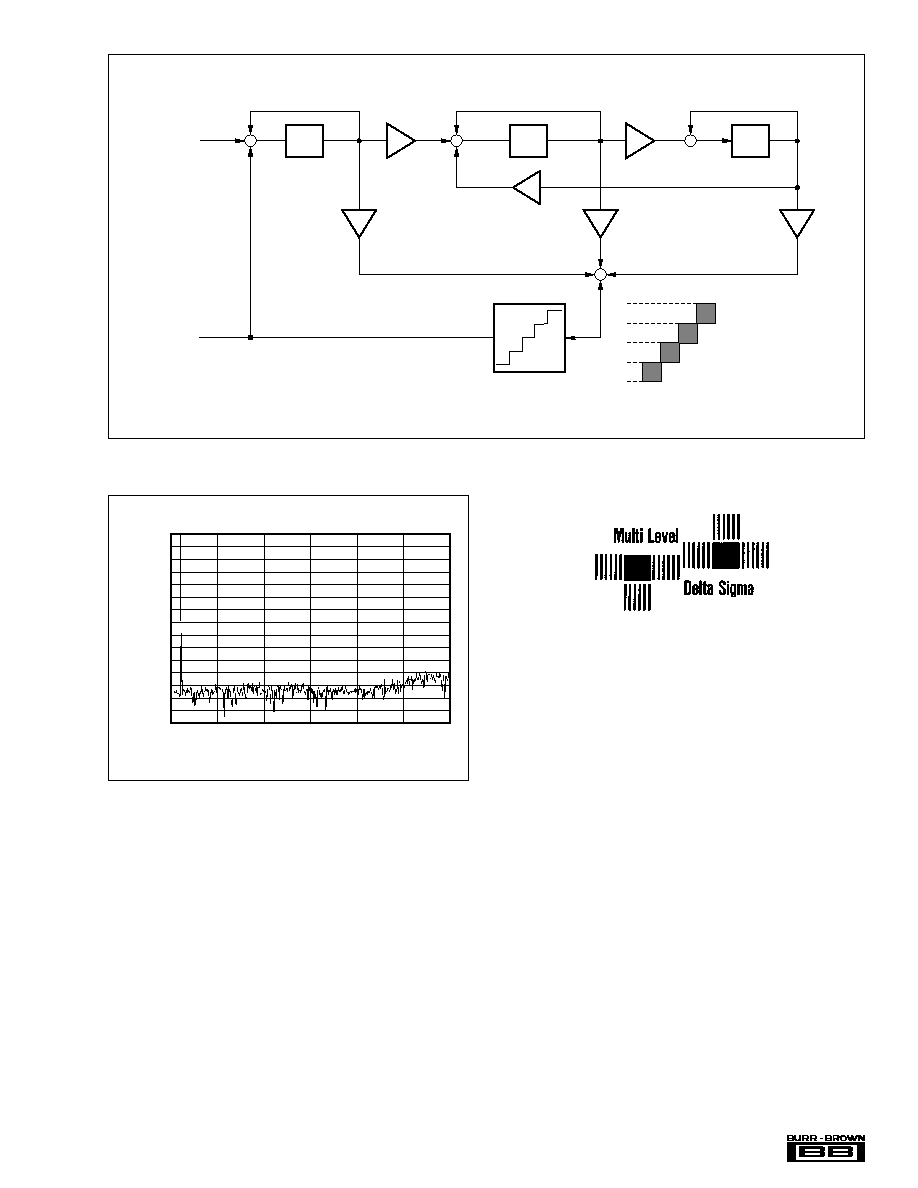
3rd ORDER
MODULATOR
Frequency (kHz)
Gain (≠dB)
0
≠10
≠20
≠30
≠40
≠50
≠60
≠70
≠80
≠90
≠100
≠110
≠120
≠130
≠140
≠150
0
5
10
15
20
25
30
FIGURE 15. Quantization Noise Spectrum.

IMPORTANT NOTICE
Texas Instruments and its subsidiaries (TI) reserve the right to make changes to their products or to discontinue
any product or service without notice, and advise customers to obtain the latest version of relevant information
to verify, before placing orders, that information being relied on is current and complete. All products are sold
subject to the terms and conditions of sale supplied at the time of order acknowledgment, including those
pertaining to warranty, patent infringement, and limitation of liability.
TI warrants performance of its semiconductor products to the specifications applicable at the time of sale in
accordance with TI's standard warranty. Testing and other quality control techniques are utilized to the extent
TI deems necessary to support this warranty. Specific testing of all parameters of each device is not necessarily
performed, except those mandated by government requirements.
Customers are responsible for their applications using TI components.
In order to minimize risks associated with the customer's applications, adequate design and operating
safeguards must be provided by the customer to minimize inherent or procedural hazards.
TI assumes no liability for applications assistance or customer product design. TI does not warrant or represent
that any license, either express or implied, is granted under any patent right, copyright, mask work right, or other
intellectual property right of TI covering or relating to any combination, machine, or process in which such
semiconductor products or services might be or are used. TI's publication of information regarding any third
party's products or services does not constitute TI's approval, warranty or endorsement thereof.
Copyright
©
2000, Texas Instruments Incorporated