Æ
1
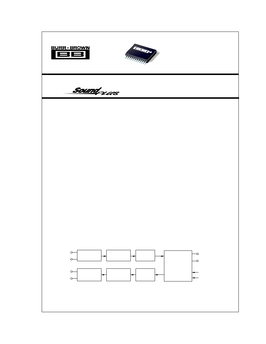
PCM3006
FEATURES
q
MONOLITHIC 16-BIT
ADC AND DAC
q
STEREO ADC:
Single-Ended Voltage Input
64 X Oversampling
High Performance
THD+N: ≠84dB
SNR: 89dB
Dynamic Range: 89dB
Digital High Pass Filter
q
STEREO DAC:
Single-Ended Voltage Output
Analog Low Pass Filter
8X Oversampling Digital Filter
High Performance
THD+N: ≠85dB
SNR: 93dB
Dynamic Range: 93dB
q
SPECIAL FEATURES
Digital De-emphasis
Power Down: ADC/DAC Independent
q
SAMPLING RATE: Up to 48kHz
q
SYSTEM CLOCK: 256f
S
, 384f
S
, 512f
S
q
SINGLE +3V POWER SUPPLY
q
SMALL PACKAGE: 24-Lead TSSOP
International Airport Industrial Park ∑ Mailing Address: PO Box 11400, Tucson, AZ 85734 ∑ Street Address: 6730 S. Tucson Blvd., Tucson, AZ 85706 ∑ Tel: (520) 746-1111 ∑ Twx: 910-952-1111
Internet: http://www.burr-brown.com/ ∑ FAXLine: (800) 548-6133 (US/Canada Only) ∑ Cable: BBRCORP ∑ Telex: 066-6491 ∑ FAX: (520) 889-1510 ∑ Immediate Product Info: (800) 548-6132
DESCRIPTION
The PCM3006 is a low cost single chip stereo audio
CODEC (analog-to-digital and digital-to-analog con-
verters) with single-ended analog voltage input and
output.
Both ADCs and DACs employ delta-sigma modula-
tion with 64X oversampling. The ADCs include a
digital decimation filter, and the DACs include an 8X
oversampling digital interpolation filter. The DACs
also include a de-emphasis function. PCM3006 oper-
ates with 16-bit, left-justified for ADC, right-justified
for DAC data formats.
PCM3006 provides a Power-Down Mode that oper-
ates on the ADCs and DACs independently.
Fabricated on a highly advanced 0.6
µ
s CMOS pro-
cess, PCM3006 is suitable for a wide variety of
cost-sensitive consumer applications where good
performance is required. Applications include sam-
pling keyboards, digital mixers, effects processors,
hard-disk recorders, data recorders and digital video
cameras.
© 1998 Burr-Brown Corporation
PDS-1436A
Printed in U.S.A. February, 1998
PCM3006
Æ
16-Bit, Single-Ended Analog Input/Output
STEREO AUDIO CODEC
TM
Lch In
Rch In
Analog Front-End
Delta-Sigma
Modulator
Decimation
Digital Filter
Serial Interface
and
Mode Control
Digital Out
Digital In
Parallel Mode Control
System Clock
Lch Out
Rch Out
Low Pass Filter
and
Output Buffer
Multi-Level
Delta-Sigma
Modulator
Oversampling
Interpolation
Digital Filter
PCM3006
SBAS089
Æ
2
PCM3006
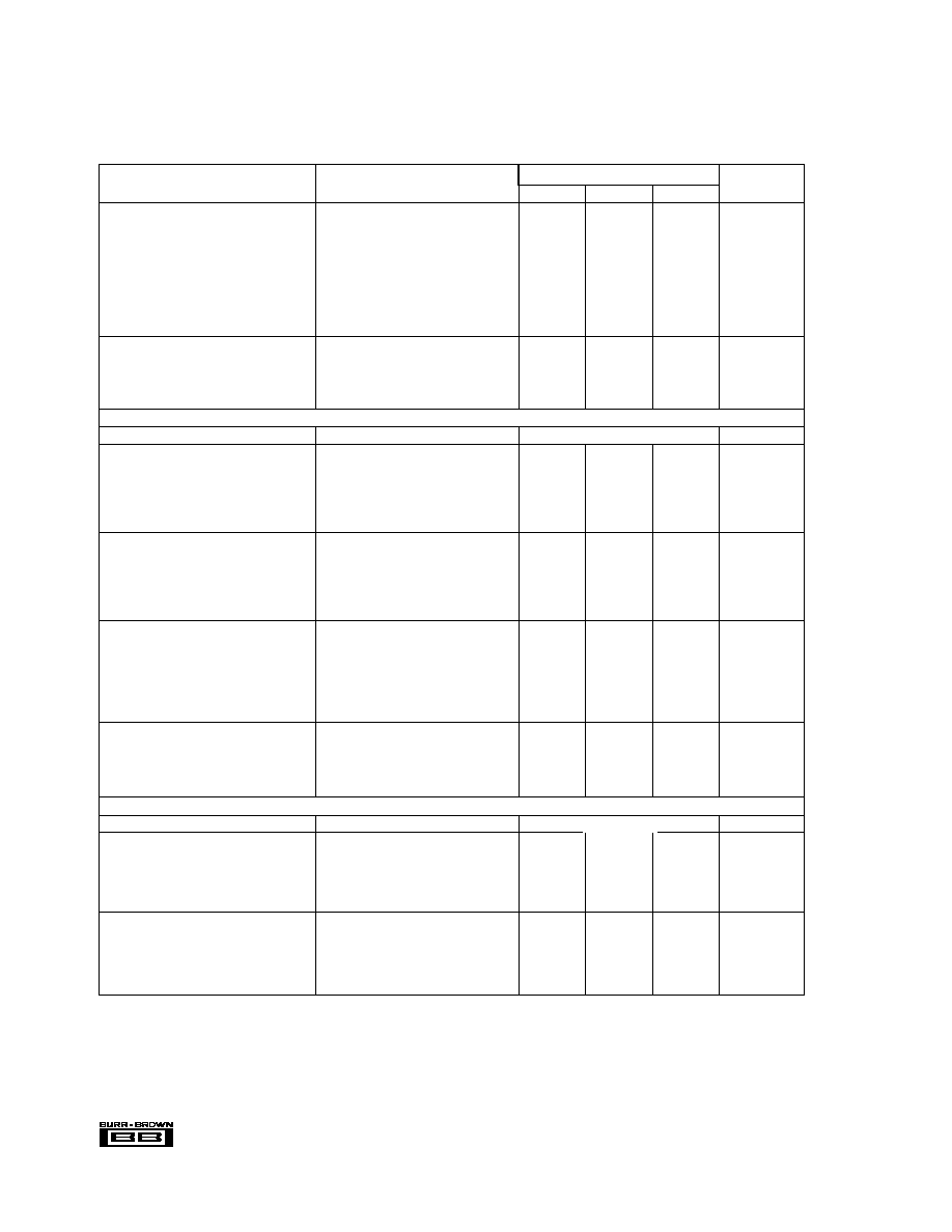
SPECIFICATIONS
All specifications at +25
∞
C, V
DD
= V
CC
= 3.0V, f
S
= 44.1kHz, SYSCLK = 384f
S
, and 16-bit data, unless otherwise noted.
The information provided herein is believed to be reliable; however, BURR-BROWN assumes no responsibility for inaccuracies or omissions. BURR-BROWN assumes no
responsibility for the use of this information, and all use of such information shall be entirely at the user's own risk. Prices and specifications are subject to change without notice.
No patent rights or licenses to any of the circuits described herein are implied or granted to any third party. BURR-BROWN does not authorize or warrant any BURR-BROWN
product for use in life support devices and/or systems.
PCM3006T
PARAMETER
CONDITIONS
MIN
TYP
MAX
UNITS
DIGITAL INPUT/OUTPUT
Input Logic
Input Logic Level: V
IH
(1)
0.7 x V
DD
VDC
V
IL
(1)
0.3 x V
DD
VDC
Input Logic Current: I
IN
(2)
±
1
µ
A
Input Logic Current: I
IN
(3)
100
µ
A
Output Logic
Output Logic Level: V
OH
(4)
I
OUT
= ≠1mA
V
DD
≠0.3
VDC
V
OL
(4)
I
OUT
= +1mA
0.3
VDC
CLOCK FREQUENCY
Sampling Frequency (f
S
)
32
44.1
48
kHz
System Clock Frequency
256f
S
8.1920
11.2896
12.2880
MHz
384f
S
12.2880
16.9344
18.4320
MHz
512f
S
16.3840
22.5792
24.5760
MHz
ADC CHARACTERISTICS
RESOLUTION
16
Bits
DC ACCURACY
Gain Mismatch Channel-to-Channel
±
1.0
±
3.0
% of FSR
Gain Error
±
2.0
±
5.0
% of FSR
Gain Drift
±
20
ppm of FSR/
∞
C
Bipolar Zero Error
High-Pass Filter Disabled
(6)
±
1.7
% of FSR
Bipolar Zero Drift
High-Pass Filter Disabled
(6)
±
20
ppm of FSR/
∞
C
DYNAMIC PERFORMANCE
(5)
THD+N: V
IN
= ≠0.5dB
≠84
≠77
dB
V
IN
= ≠60dB
≠26
dB
Dynamic Range
A-Weighted
84
89
dB
Signal-to-Noise Ratio
A-Weighted
84
89
dB
Channel Separation
82
86
dB
DIGITAL FILTER PERFORMANCE
Passband
0.454f
S
Hz
Stopband
0.583f
S
Hz
Passband Ripple
±
0.05
dB
Stopband Attenuation
≠65
dB
Delay Time
17.4/f
S
sec
HPF Frequency Response
≠3dB
0.019f
S
mHz
ANALOG INPUT
Voltage Range
0.60 V
CC
Vp-p
Center Voltage
0.50 V
CC
V
Input Impedance
30
k
Anti-Aliasing Filter Frequency Response
≠3dB
150
kHz
DAC CHARACTERISTICS
RESOLUTION
16
Bits
DC ACCURACY
Gain Mismatch Channel-to-Channel
±
1.0
±
3
% of FSR
Gain Error
±
1.0
±
5
% of FSR
Gain Drift
±
20
ppm of FSR/
∞
C
Bipolar Zero Error
±
2.5
% of FSR
Bipolar Zero Drift
±
20
ppm of FSR/
∞
C
DYNAMIC PERFORMANCE
(6)
THD+N: V
OUT
= 0dB (Full Scale)
≠85
≠77
dB
V
OUT
= ≠60dB
≠30
dB
Dynamic Range
EIAJ, A-Weighted
86
93
dB
Signal-to-Noise Ratio
EIAJ, A-Weighted
86
93
dB
Channel Separation
84
90
dB
Æ
3
PCM3006
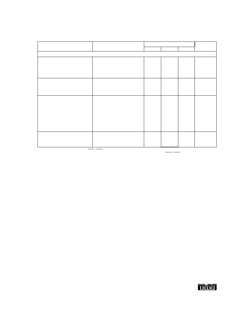
SPECIFICATIONS
(CONT)
All specifications at +25
∞
C, V
DD
= V
CC
= 3.0V, f
S
= 44.1kHz, SYSCLK = 384f
S
, CLKIO Input, 16-bit data, unless otherwise noted.
PCM3006T
PARAMETER
CONDITIONS
MIN
TYP
MAX
UNITS
DAC CHARACTERISTICS (CONT)
DIGITAL FILTER PERFORMANCE
Passband
0.445f
S
Hz
Stopband
0.555f
S
Hz
Passband Ripple
±
0.17
dB
Stopband Attenuation
≠35
dB
Delay Time
11.1/f
S
sec
ANALOG OUTPUT
Voltage Range
0.6 x V
CC
Vp-p
Center Voltage
0.5 x V
CC
VDC
Load Impedance
AC-Coupling
10
k
LPF Frequency Response
f = 20kHz
≠0.16
dB
POWER SUPPLY REQUIREMENTS
Voltage Range: V
CC
, V
DD
≠25
∞
C to +85
∞
C
2.7
3.0
3.6
VDC
0
∞
C to +70
∞
C
(7)
2.4
3.0
3.6
VDC
Supply Current: ADC/DAC Operation
V
CC
= V
DD
= 3.0V
18
24
mA
ADC Operation
V
CC
= V
DD
= 3.0V
12
16
mA
DAC Operation
V
CC
= V
DD
= 3.0V
7
10
mA
ADC/DAC Power-Down
(8)
V
CC
= V
DD
= 3.0V
50
µ
A
Power Dissipation: ADC/DAC Operation
V
CC
= V
DD
= 3.0V
54
72
mW
ADC Operation
V
CC
= V
DD
= 3.0V
36
48
mW
DAC Operation
V
CC
= V
DD
= 3.0V
21
30
mW
ADC/DAC Power-Down
(8)
V
CC
= V
DD
= 3.0V
150
µ
W
TEMPERATURE RANGE
Operation
≠25
+85
∞
C
Storage
≠55
+125
∞
C
Thermal Resistance,
JA
100
∞
C/W
NOTES: (1) Pins 7, 8, 9, 10, 11, 15, 17, 18: PDAD, PDDA, SYSCLK, LRCIN, BCKIN, DIN, DEM1, DEM0 (Schmitt-Trigger input with 100k
typical internal pull-
down resistor). (2) Pins 9, 10, 11, 15: SYSCLK, LRCIN, BCKIN, DIN (Schmitt-Trigger input). (3) Pins 7, 8, 17, 18: PDAD, PDDA, DEM1, DEM0 (Schmitt-Trigger
input, 100k
typical internal pull-down resistor). (4) Pin 12: DOUT. (5) f
IN
= 1kHz, using Audio Precision System II, rms mode with 20kHz LPF, 400Hz HPF used
for performance calculation. (6) f
OUT
= 1kHz, using Audio Precision System II, rms mode with 20kHz LPF, 400Hz HPF used for performance calculation. (7) Applies
for voltages between 2.4V to 2.7V for 0
∞
C to +70
∞
C and 256f
S
/512f
S
operation (384f
S
not available). (8) SYSCLK, BCKIN, and LRCIN are stopped.
Æ
4
PCM3006
V
CC
1
V
CC
1
V
IN
R
V
REF
1
V
REF
2
V
IN
L
PDAD
PDDA
SYSCLK
LRCIN
BCKIN
DOUT
V
CC
2
NC
AGND
V
COM
V
OUT
R
V
OUT
L
DEM0
DEM1
NC
DIN
V
DD
DGND
1
2
3
4
5
6
7
8
9
10
11
12
24
23
22
21
20
19
18
17
16
15
14
13
PCM3006
NC = No Connection
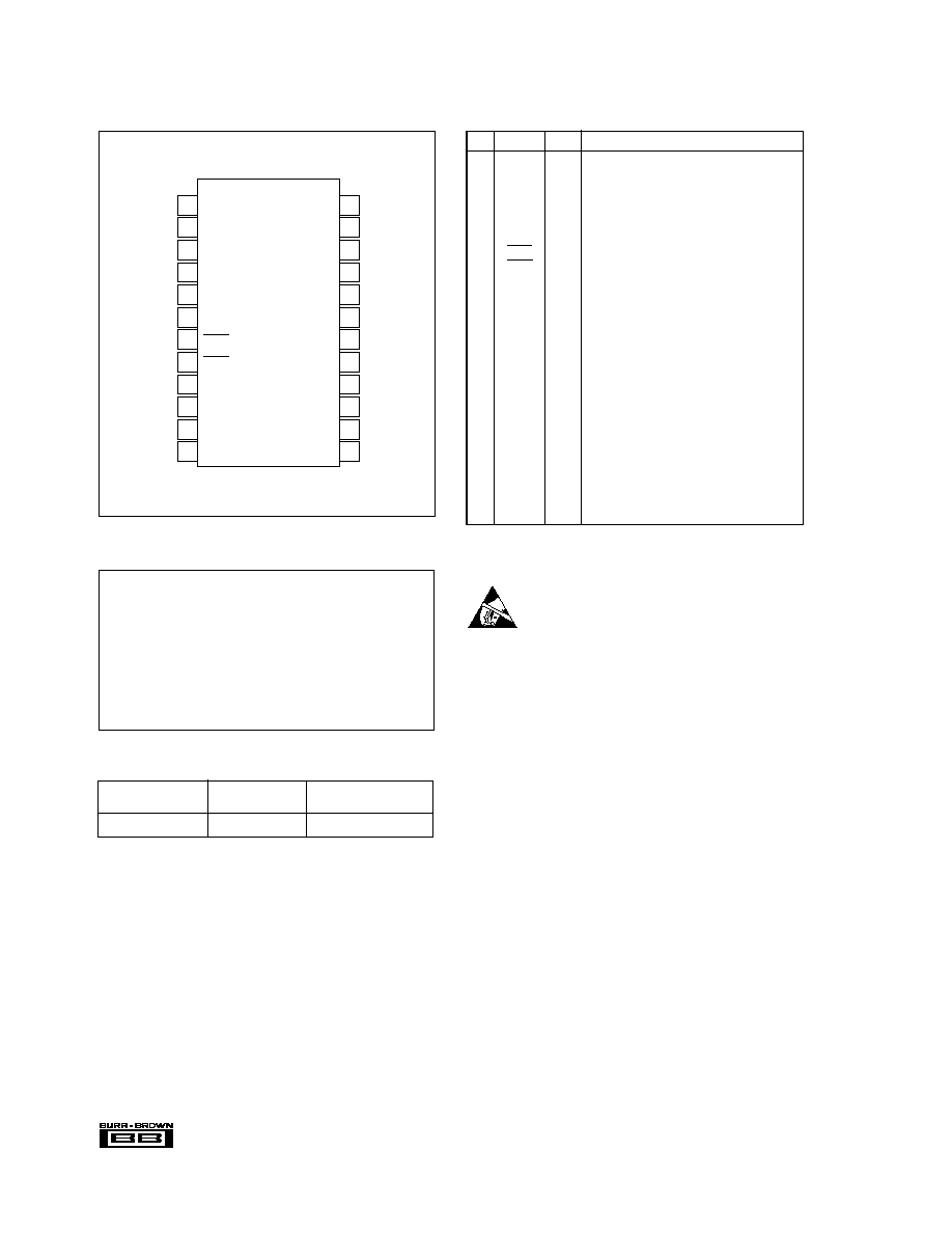
PIN CONFIGURATION
Top View
TSSOP
PIN
NAME
I/O
DESCRIPTION
1
V
CC
1
--
ADC Analog Power Supply
2
V
CC
1
--
ADC Analog Power Supply
3
V
IN
R
IN
ADC Analog Input, Rch
4
V
REF
1
--
ADC Reference, 1
5
V
REF
2
--
ADC Reference, 2
6
V
IN
L
IN
ADC Analog Input, Lch
7
PDAD
IN
ADC Power Down, Active LOW
(1, 2)
8
PDDA
IN
DAC Power Down, Active LOW
(1, 2)
9
SYSCLK
IN
System Clock Input
(2)
10
LRCIN
IN
Sample Rate Clock Input (f
S
)
(2)
11
BCKIN
IN
Bit Clock Input
(2)
12
DOUT
OUT
Data Output
13
DGND
--
Digital Ground
14
V
DD
--
Digital Power Supply
15
DIN
IN
Data Input
16
NC
IN
No Connection
17
DEM1
IN
De-emphasis Control
(1, 2)
18
DEM0
IN
De-emphasis Control 0
(1, 2)
19
V
OUT
L
OUT
DAC Analog Output, Lch
20
V
OUT
R
OUT
DAC Analog Output, Rch
21
V
COM
--
ADC/DAC Common
22
AGND
--
Analog Ground
23
NC
--
No Connection
24
V
CC
2
--
DAC Analog Power Supply
NOTES: (1) With 100k
typical internal pull-down resistor. (2) Schmitt-Trigger
input.
PIN ASSIGNMENTS
Supply Voltage
+V
DD
, +V
CC
1, +V
CC
2 ...................................................................... +6.5V
Supply Voltage Differences ...............................................................
±
0.1V
GND Voltage Differences ..................................................................
±
0.1V
Digital Input Voltage ...................................................... ≠0.3 to V
DD
+ 0.3V
Analog Input Voltage ......................................... ≠0.3 to V
CC
1,
V
CC
2 + 0.3V
Power Dissipation .......................................................................... 300mW
Input Current ...................................................................................
±
10mA
Operating Temperature Range ......................................... ≠25
∞
C to +85
∞
C
Storage Temperature ...................................................... ≠55
∞
C to +125
∞
C
Lead Temperature (soldering, 5s) .................................................. +260
∞
C
(reflow, 10s) ..................................................... +235
∞
C
ABSOLUTE MAXIMUM RATINGS
ELECTROSTATIC
DISCHARGE SENSITIVITY
This integrated circuit can be damaged by ESD. Burr-Brown
recommends that all integrated circuits be handled with
appropriate precautions. Failure to observe proper handling
and installation procedures can cause damage.
ESD damage can range from subtle performance degrada-
tion to complete device failure. Precision integrated circuits
may be more susceptible to damage because very small
parametric changes could cause the device not to meet its
published specifications.
PACKAGE INFORMATION
PACKAGE DRAWING
PRODUCT
PACKAGE
NUMBER
(1)
PCM3006T
24-Lead TSSOP
350
NOTE: (1) For detailed drawing and dimension table, please see end of data
sheet, or Appendix C of Burr-Brown IC Data Book.
Æ
5
PCM3006
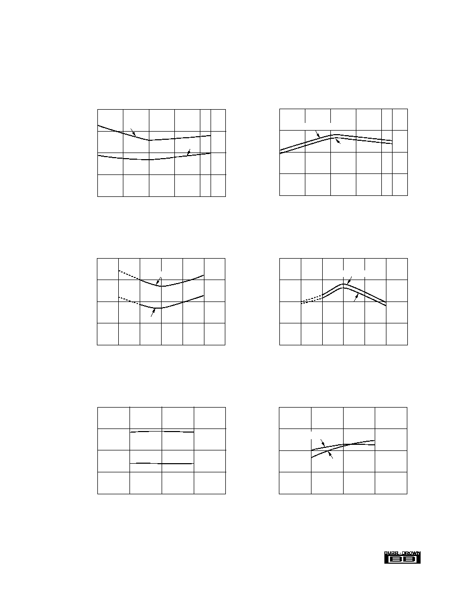
TYPICAL PERFORMANCE CURVES
ADC SECTION
At T
A
= +25
∞
C, V
CC
= V
DD
= 3.0V, f
S
= 44.1kHz, f
SYSCLK
= 384f
S
, and f
SIGNAL
= 1kHz, unless otherwise noted.
THD+N vs TEMPERATURE
Temperature (∞C)
THD+N at ≠0.5dB (%)
0.010
0.008
0.006
0.004
0.002
≠25
0
25
50
75
85
100
THD+N at ≠60dB (%)
6.0
5.0
4.0
3.0
2.0
≠60dB
0.5dB
DYNAMIC RANGE and SNR vs TEMPERATURE
Temperature (∞C)
Dynamic Range (dB)
92
90
88
86
84
≠25
0
25
50
75
85
100
SNR (dB)
92
90
88
86
84
SNR
Dynamic Range
DYNAMIC RANGE and SNR vs SUPPLY VOLTAGE
Supply Voltage
(V)
Dynamic Range (dB)
92
90
88
86
84
2.4
2.7
3.0
3.3
3.6
SNR (dB)
92
90
88
86
84
Dynamic Range
SNR
THD+N vs SUPPLY VOLTAGE
Supply Voltage
(V)
THD+N at ≠0.5dB (%)
0.010
0.008
0.006
0.004
0.002
2.4
2.7
3.0
3.3
3.6
THD+N at ≠60dB (%)
6.0
5.0
4.0
3.0
2.0
≠60dB
≠0.5dB
THD+N vs SAMPLING FREQUENCY
f
S
(kHz)
THD+N at ≠0.5dB (%)
0.010
0.008
0.006
0.004
0.002
32
44.1
48
THD+N at ≠60dB (%)
5.0
4.0
3.0
2.0
1.0
≠60dB
≠0.5dB
DYNAMIC RANGE and SNR vs SAMPLING FREQUENCY
f
S
(kHz)
Dynamic Range (dB)
92
90
88
86
84
32
44.1
48
SNR (dB)
92
90
88
86
84
Dynamic Range
SNR

Æ
6
PCM3006
TYPICAL PERFORMANCE CURVES
DAC SECTION
At T
A
= +25
∞
C, V
CC
= V
DD
= 3.0V, f
S
= 44.1kHz, f
SYSCLK
= 384f
S
, and f
SIGNAL
= 1kHz, unless otherwise noted.
THD+N vs TEMPERATURE
Temperature (∞C)
THD+N at FS (%)
0.010
0.008
0.006
0.004
0.002
≠25
0
25
50
75
85
100
THD+N at ≠60dB (%)
4.0
3.0
2.0
1.0
0
FS
≠60dB
DYNAMIC RANGE and SNR vs TEMPERATURE
Temperature (∞C)
Dynamic Range (dB)
96
94
92
90
88
≠25
0
25
50
75
85
100
SNR (dB)
96
94
92
90
88
SNR
Dynamic Range
THD+N vs SUPPLY VOLTAGE
Supply Voltage
(V)
THD+N at FS (%)
0.010
0.008
0.006
0.004
0.002
2.4
2.7
3.0
3.3
3.6
THD+N at ≠60dB (%)
4.0
3.0
2.0
1.0
0
≠60dB
FS
DYNAMIC RANGE and SNR vs SUPPLY VOLTAGE
Supply Voltage
(V)
Dynamic Range (dB)
96
94
92
90
88
2.4
2.7
3.0
3.3
3.6
SNR (dB)
96
94
92
90
88
SNR
Dynamic Range
THD+N vs SAMPLING FREQUENCY
and SYSTEM CLOCK
f
S
(kHz)
THD+N at FS (%)
0.010
0.008
0.006
0.004
0.002
32
44.1
48
THD+N at ≠60dB (%)
4.0
3.0
2.0
1.0
0
≠60dB
384f
S
256f
S
, 512f
S
384f
S
256f
S
, 512f
S
FS
DYNAMIC RANGE and SNR
vs SAMPLING FREQUENCY and SYSTEM CLOCK
f
S
(kHz)
Dynamic Range (dB)
96
94
92
90
88
32
44.1
48
SNR (dB)
96
94
92
90
88
384f
S
256f
S
, 512f
S
SNR
Dynamic
Range
Æ
7
PCM3006
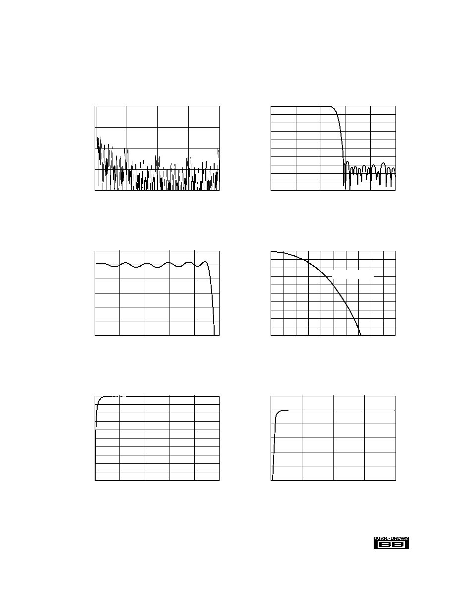
TYPICAL PERFORMANCE CURVES
At T
A
= +25
∞
C, V
CC
= V
DD
= 3.0V, f
S
= 44.1kHz, and f
SYSCLK
= 384f
S
, unless otherwise noted.
ADC DIGITAL FILTER
STOPBAND ATTENUATION CHARACTERISTICS
Normalized Frequency (x f
S
Hz)
Amplitude (dB)
0
≠10
≠20
≠30
≠40
≠50
≠60
≠70
≠80
≠90
≠100
0.2
0.4
0.6
0.8
1.0
0
PASSBAND RIPPLE CHARACTERISTICS
Normalized Frequency (x f
S
Hz)
Amplitude (dB)
0.2
0.0
≠0.2
≠0.4
≠0.6
≠0.8
≠1.0
0.1
0.2
0.3
0.4
0.5
0
TRANSIENT BAND CHARACTERISTICS
Normalized Frequency (x f
S
Hz)
Amplitude (dB)
0
≠1
≠2
≠3
≠4
≠5
≠6
≠7
≠8
≠9
≠10
0.45
0.46 0.47 0.48 0.49
0.50 0.51
0.52 0.53 0.54 0.55
≠4.13dB at 0.5 x f
S
HIGH PASS FILTER RESPONSE
Normalized Frequency (x f
S
/1000 Hz)
Amplitude (dB)
0
≠10
≠20
≠30
≠40
≠50
≠60
≠70
≠80
≠90
≠100
0.1
0.2
0.3
0.4
0.5
0
HIGH PASS FILTER RESPONSE
Normalized Frequency (x f
S
/1000 Hz)
Amplitude (dB)
0.2
0.0
≠0.2
≠0.4
≠0.6
≠0.8
≠1.0
1
2
3
4
0
OVERALL CHARACTERISTICS
Normalized Frequency (x f
S
Hz)
Amplitude (dB)
0
≠50
≠100
≠150
≠200
8
16
24
32
0

Æ
8
PCM3006
TYPICAL PERFORMANCE CURVES
At T
A
= +25
∞
C, V
CC
= V
DD
= 3.0V, f
S
= 44.1kHz, and f
SYSCLK
= 384f
S
, unless otherwise noted.
ANTI-ALIASING FILTER
ANTI-ALIASING FILTER OVERALL
FREQUENCY RESPONSE
Frequency (Hz)
Amplitude (dB)
0
≠10
≠20
≠30
≠40
≠50
10
100
1k
10k
100k
1M
10M
0
ANTI-ALIASING FILTER PASSBAND
FREQUENCY RESPONSE
Frequency (Hz)
Amplitude (dB)
0.2
0.0
≠0.2
≠0.4
≠0.6
≠0.8
≠1.0
10
100
1k
10k
100k
0
Æ
9
PCM3006
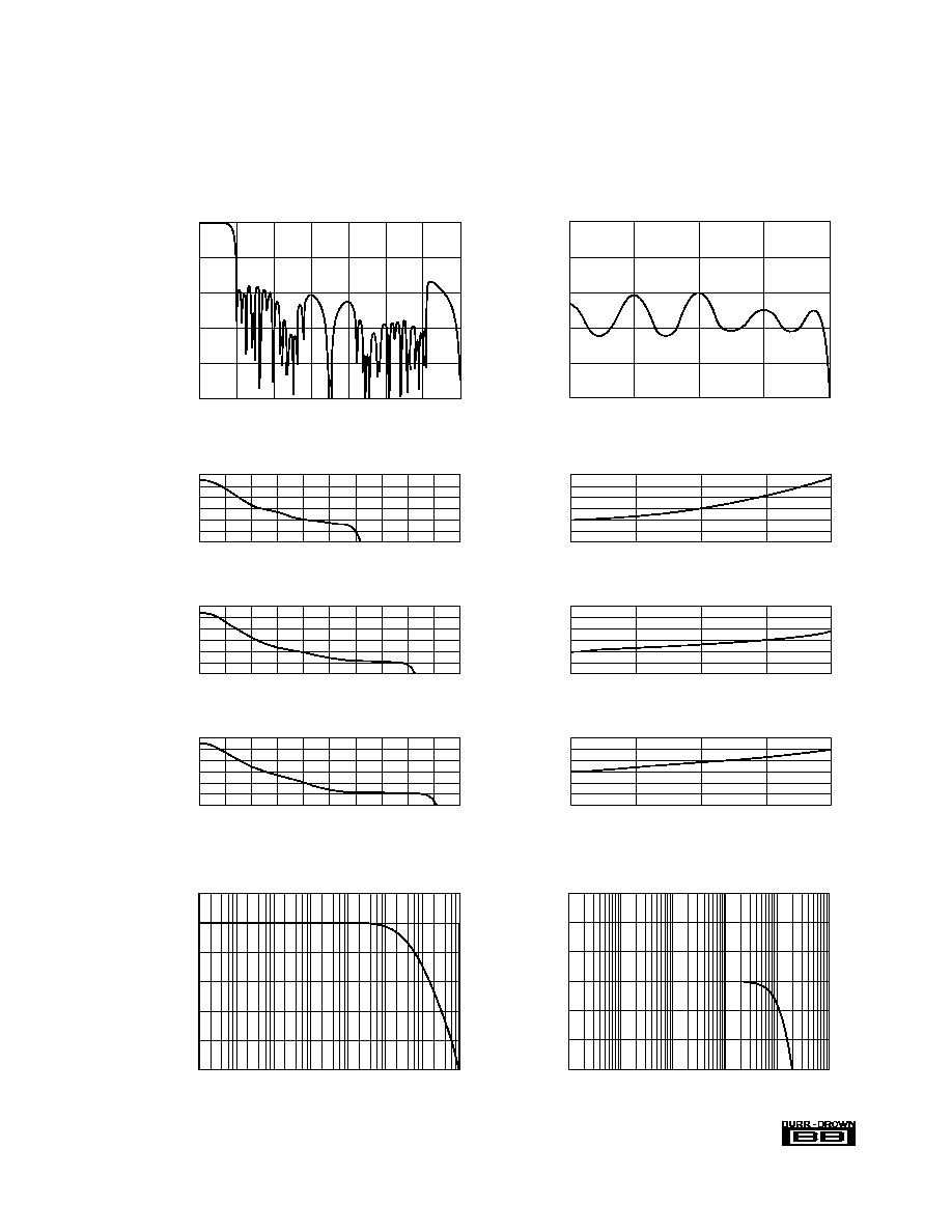
TYPICAL PERFORMANCE CURVES
At T
A
= +25
∞
C, V
CC
= V
DD
= 3.0V, f
S
= 44.1kHz, and f
SYSCLK
= 384f
S
, unless otherwise noted.
DAC DIGITAL FILTER
0
50k
100k
150k
0
≠20
≠40
≠60
≠80
≠100
Level (dB)
OVERALL FREQUENCY CHARACTERISTICS
(f
S
= 44.1kHz)
Frequency (Hz)
PASSBAND RIPPLE CHARACTERISTICS (f
S
= 44.1kHz)
0
≠0.2
≠0.4
≠0.6
≠0.8
≠1.0
0
5k
10k
15k
20k
Level (dB)
Frequency (Hz)
DE-EMPHASIS FREQUENCY RESPONSE (32kHz)
0
5k
10k
15k
20k
25k
Frequency (Hz)
0
≠2
≠4
≠6
≠8
≠10
≠12
DE-EMPHASIS FREQUENCY RESPONSE (44.1kHz)
0
5k
10k
15k
20k
25k
Frequency (Hz)
0
≠2
≠4
≠6
≠8
≠10
≠12
DE-EMPHASIS FREQUENCY RESPONSE (48kHz)
0
5k
10k
15k
20k
25k
Frequency (Hz)
0
≠2
≠4
≠6
≠8
≠10
≠12
Level (dB)
Level (dB)
Level (dB)
DE-EMPHASIS ERROR (32kHz)
0
3628
7256
10884
14512
0
4999.8375
9999.675
14999.5125
19999.35
0
5442
10884
16326
21768
Frequency (Hz)
0.6
0.4
0.2
0
≠0.2
≠0.4
≠0.6
0.6
0.4
0.2
0
≠0.2
≠0.4
≠0.6
0.6
0.4
0.2
0
≠0.2
≠0.4
≠0.6
DE-EMPHASIS ERROR (44.1kHz)
Frequency (Hz)
DE-EMPHASIS ERROR (48kHz)
Frequency (Hz)
Error (dB)
Error (dB)
Error (dB)
20
0
≠20
≠40
≠60
≠80
≠100
10
100
1k
10k
100k
1M
10M
Frequency (Hz)
Level (dB)
INTERNAL ANALOG FILTER FREQUENCY RESPONSE
(10Hz~10MHz)
0.15
0.10
0.05
0
≠0.05
≠0.10
≠0.15
Level (dB)
1
Frequency (Hz)
10
100
1k
10k
100k
INTERNAL ANALOG FILTER FREQUENCY RESPONSE
(1Hz~20kHz)
Æ
10
PCM3006
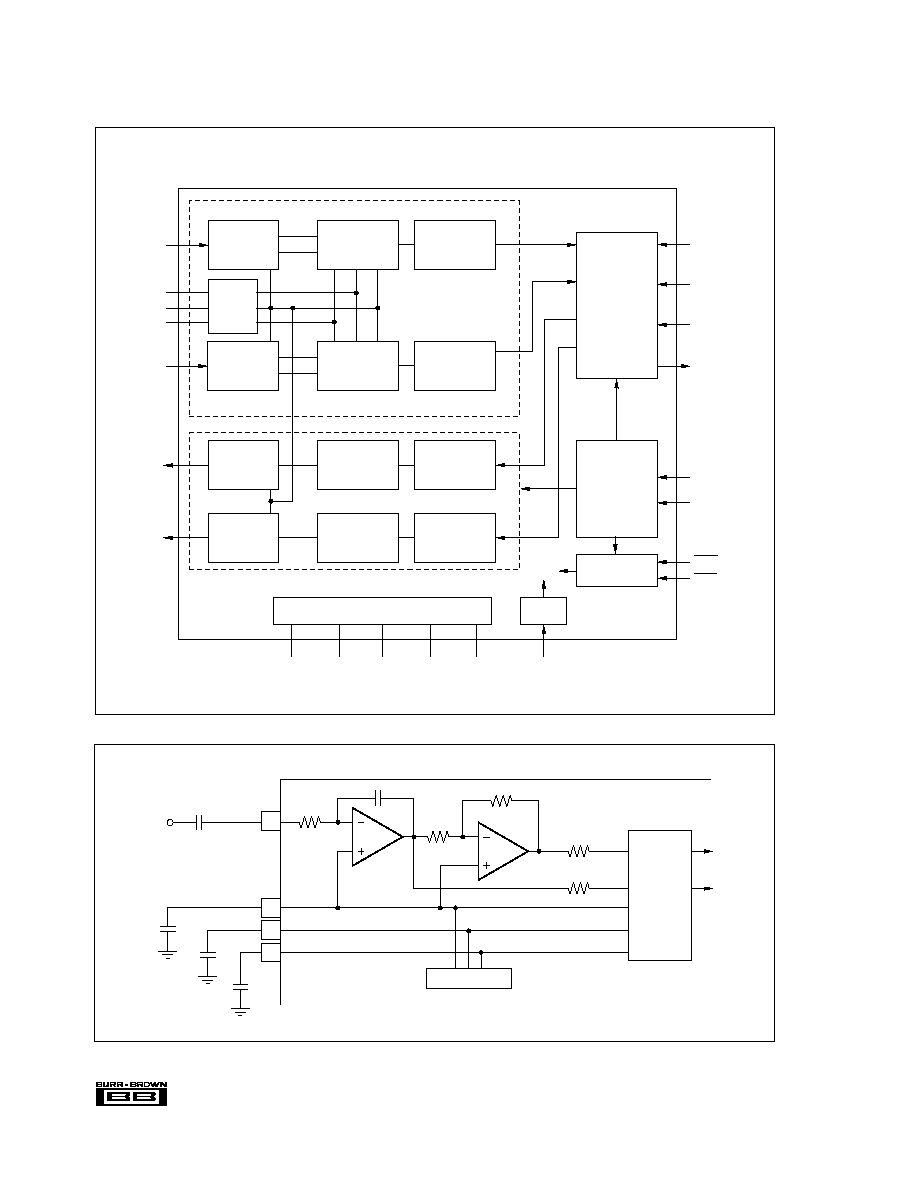
BLOCK DIAGRAM
FIGURE 1. Analog Front-End (Single-Channel).
Interpolation
Filter
8X Oversampling
Interpolation
Filter
8X Oversampling
Multi-Level
Delta-Sigma
Modulator
Multi-Level
Delta-Sigma
Modulator
Clock
Reset and
Power Down
PDDA
SYSCLK
V
CC
2
AGND
V
CC
1
PDAD
Reference
Mode
Control
Interface
DEM0
DEM1
Serial Data
Interface
DOUT
BCKIN
LRCIN
DIN
V
IN
L
V
REF
1
V
COM
V
REF
2
V
IN
R
V
OUT
L
V
OUT
R
Power Supply
DGND
V
DD
Analog
Low-Pass
Filter
Analog
Low-Pass
Filter
Decimation
and
High Pass Filter
Delta-Sigma
Modulator
(≠)
(+)
Analog
Front-End
Circuit
Decimation
and
High Pass Filter
Delta-Sigma
Modulator
ADC
DAC
(+)
(≠)
Analog
Front-End
Circuit
30k
V
IN
R
1
21
4
5
V
COM
V
REF
1
V
REF
2
Delta-Sigma
Modulator
(+)
(≠)
V
REF
+
+
1.0µF
4.7µF
+
4.7µF
+
4.7µF
Æ
11
PCM3006
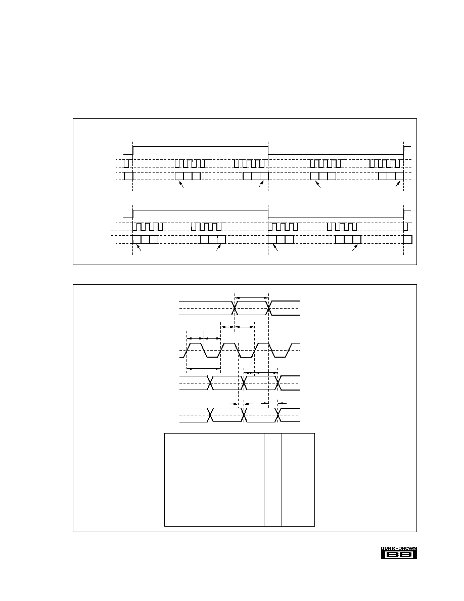
PCM AUDIO INTERFACE
The four-wire digital audio interface for PCM3006 is com-
prised of: LRCIN (pin 10), BCKIN (pin 11), DIN (pin 15),
and DOUT (pin 12). PCM3006 accepts 16-bit Most Signifi-
cant Bit (MSB) First. Figures 2 and 3 illustrate audio data
input/output format and timing.
PCM3006 can accept 32-, 48-, or 64-bit clocks (BCKIN) in
one clock of LRCIN.
MSB
L≠ch
R≠ch
L≠ch
R≠ch
LSB
LRCIN
BCKIN
FORMAT 0: PCM3006
DIN
MSB
LSB
DAC: 16-Bit, MSB-First, Right-Justified
ADC: 16-Bit, MSB-First, Left-Justified
1
16
2
3
14 15 16
1
2
3
14 15 16
MSB
LSB
LRCIN
BCKIN
DOUT
MSB
LSB
1
2
3
14 15 16
1
2
3
14 15 16
1
FIGURE 2. Audio Data Input/Output Format.
t
BCH
t
BCY
t
BCL
t
LB
t
DIH
t
DIS
t
LRP
t
BL
t
LDO
t
BDO
BCKIN
LRCIN
DIN
DOUT
0.5V
DD
0.5V
DD
0.5V
DD
0.5V
DD
BCKIN Pulse Cycle Time
t
BCY
300ns (min)
BCKIN Pulse Width High
t
BCH
120ns (min)
BCKIN Pulse Width Low
t
BCL
120ns (min)
BCKIN Rising Edge to LRCIN Edge
t
BL
40ns (min)
LRCIN Edge to BCKIN Rising Edge
t
LB
40ns (min)
LRCIN Pulse Width
t
LRP
t
BCY
(min)
DIN Set-up Time
t
DIS
40ns (min)
DIN Hold Time
t
DIH
40ns (min)
DOUT Delay Time to BCKIN Falling Edge
t
BDO
40ns (max)
DOUT Delay Time to LRCIN Edge
t
LDO
40ns (max)
Rising Time of All Signals
t
RISE
20ns (max)
Falling Time of All Signals
t
FALL
20ns (max)
FIGURE 3. Audio Data Input/Output Timing.
Æ
12
PCM3006
SYSTEM CLOCK
The system clock for PCM3006 must be either 256f
S
, 384f
S
or 512f
S
, where f
S
is the audio sampling frequency. The
system clock should be provided to SYSCLK (pin 9).
PCM3006 also has a system clock detection circuit which
automatically senses if the system clock is operating at 256f
S
,
384f
S
, or 512f
S
. When 384f
S
or 512f
S
system clock is used,
the clock is divded into 256f
S
automatically. The 256f
S
clock
is used to operate the digital filter and the delta-sigma
modulator.
Table I lists the relationship of typical sampling frequencies
and system clock frequencies and Figure 4 illustrates the
system clock timing.
FIGURE 5. Internal Power-On Reset Timing.
1024 System Clock Periods
Reset
Reset Removal
2.4V
2.2V
2.0V
V
DD
Internal Reset
System Clock
FIGURE 6. External Forced Reset Timing.
1024 System Clock Periods
Reset
Reset Removal
System Clock
Internal Reset
PDAD and PDDA
t
RST
PDAD = LOW and PDDA = LOW Pulse Width
t
RST
= 40ns minimum
System Clock Pulse Width High
t
SCKH
12ns(min)
System Clock Pulse Width Low
t
SCKL
12ns(min)
t
SCKH
t
SCKL
1/256f
S
,1/384f
S
,or 1/512f
S
0.7V
DD
"H"
SYSCLK
"L"
0.3V
DD
FIGURE 4. System Clock Timing.
SAMPLING RATE FREQUENCY
SYSTEM CLOCK FREQUENCY
(kHz)
(MHz)
256f
S
384f
S
512f
S
32
8.1920
12.2880
16.3840
44.1
11.2896
16.9340
22.5792
48
12.2880
18.4320
24.5760
TABLE I. System Clock Frequencies.
RESET
PCM3006 has an internal Power-On Reset circuit, as well
as an external forced reset. The internal Power-On Reset
initializes (resets) when the supply voltage V
DD
>2.0V
(typ). External forced reset occurs when PDAD = LOW or
PDDA = LOW. Figure 5 shows the internal Power-On
reset timing and Figure 6 shows the external forced reset
timing by PDAD or PDDA. During external forced reset,
the outputs of the DAC are forced to GND (see Figure 7).
The analog outputs are then forced to 0.5V
CC
during
t
DACDLY1
(16384/f
S
) after reset removal. The outputs of
ADC are also invalid, digital outputs are forced to all zero
during t
ADCDLY1
(18432/f
S
) after reset removal.
Æ
13
PCM3006
SYNCHRONIZATION WITH THE DIGITAL AUDIO
SYSTEM
PCM3006 operates with LRCIN synchronized to the system
clock. PCM3006 does not require any specific phase relation-
ship between LRCIN and the system clock, but there must be
synchronization. If the synchronization between the system
clock and LRCIN changes more than 6 bit clocks (BCKIN)
during one sample (LRCIN) period because of phase jitter on
LRCIN, internal operation of the DAC will stop within 1/f
S
,
and the analog output will be forced to bipolar zero (0.5V
CC
)
until the system clock is re-synchronized to LRCIN followed
by t
DACDLY2
delay time. Internal operation of the ADC will
also stop within 1/f
S
, and the digital output codes will be set
to bipolar zero until re-synchronization occurs followed by
t
ADCDLY2
delay time. If LRCIN is synchronized with 5 or less
bit clocks to the system clock, operation will be normal.
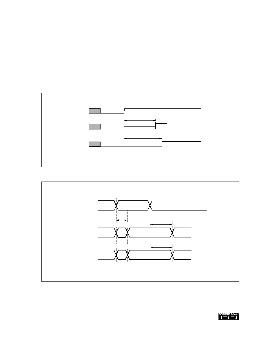
Figures 7 and 8 illustrate the effects on the output when
synchronization is lost. Before the outputs are forced to
bipolar zero (<1/f
S
seconds), the outputs are not defined and
some noise may occur. During the transitions between normal
data and undefined states, the output has discontinuities,
which will cause output noise.
FIGURE 7. DAC Output and ADC Output for Reset and Power Down.
FIGURE 8. DAC Output and ADC Output for Loss of Synchronization.
Synchronous
Asynchronous
Synchronization
Lost
Resynchronization
within
1/f
S
Synchronous
Normal
Normal
t
ADCDLY2
(32/f
S
)
t
DACDLY2
(32/f
S
)
Undefined Data
V
COM
(= 1/2 x V
CC
)
Undefined Data
State of
Synchronization
DAC V
OUT
Normal
Normal
(1 )
Zero
ADC DOUT
NOTES: (1) The HPF transient response (exponentially attenuated signal from ±0.2% DC of FSR
with 200ms time constant) appears initially.
Reset
Power Down
GND
V
COM
(0.5V
CC
)
Ready/Operation
Internal Reset
or Power Down
ADC DOUT
DAC V
OUT
Zero
Zero
Normal Data
(1)
t
ADCDLY1
(18432/f
S
)
t
DACDLY1
(16384/f
S
)
Reset Removal or Power Down OFF
NOTE: (1) The HPF transient response (exponentially attenuated signal from ±0.2% DC of FSR
with 200ms time constant) appears initially.

Æ
14
PCM3006
GROUNDING
In order to optimize the dynamic performance of PCM3006,
the analog and digital grounds are not connected internally.
The PCM3006 performance is optimized with a single
ground plane for all returns. It is recommended to tie all
PCM3006 ground pins with low impedance connections to
the analog ground plane. PCM3006 should reside entirely
over this plane to avoid coupling high frequency digital
switching noise into the analog ground plane.
VOLTAGE INPUT PINS
A tantalum capacitor, between 1
µ
F and 10
µ
F, is recom-
mended as an AC-coupling capacitor at the inputs. Combined
with the 30k
characteristic input impedance, a 1.0
µ
F cou-
pling capacitor will establish a 5.3Hz cut-off frequency for
blocking DC. The input voltage range can be increased by
adding a series resistor on the analog input line. This series
resistor, when combined with the 30k
input impedance,
creates a voltage divider and enables larger input ranges.
V
REF
Pins
A 4.7
µ
F to 10
µ
F tantalum capacitor is recommended be-
tween V
REF
1, V
REF
2, and AGND to ensure low source
impedance for the ADC's references. These capacitors should
be located as close as possible to the reference pins to reduce
dynamic errors on the ADC reference.
V
COM
Pin
A 4.7
µ
F to 10
µ
F tantalum capacitor is recommended be-
tween V
COM
and AGND to insure low source impedance of
the ADC and DAC common voltage. This capacitor should
be located as close as possible to the V
COM
pin to reduce
dynamic errors on the DAC common.
SYSTEM CLOCK
The quality of the system clock can influence dynamic
performance of both the ADC and DAC in the PCM3006.
The duty cycle and jitter at the system clock input pin must
be carefully managed. When power is supplied to the part,
the system clock, bit clock (BCKIN) and a word clock
(LCRIN) should also be supplied simultaneously. Failure to
supply the audio clocks will result in a power dissipation
increase of up to three times normal dissipation and may
degrade long term reliability if the maximum power dissipa-
tion limit is exceeded.
RST CONTROL
If the capacitance between V
REF
and V
COM
exceeds 2.2
µ
F,
an external reset control delay time circuit must be used.
OPERATIONAL CONTROL
PCM3006 has hardwire functional control using PDAD (pin
7) and PDDA (pin 8) for Power-Down Control and DEM0
(pin 18) and DEM1 (pin 17) for de-emphasis.
PDAD:
ADC Power-Down Control (Pin 7)
This pin places the ADC section in the lowest
power consumption mode. The ADC operation is
stopped by cutting the supply current to the ADC
section, and DOUT is fixed to zero during ADC
Power-Down Mode enable. Figure 7 illustrates
the ADC DOUT response for ADC power-down
ON/OFF. This does not affect the DAC operation.
PDAD
POWER-DOWN
Low
ADC Power-Down Mode Enabled
High
ADC Power-Down Mode Disabled
PDDA:
DAC Power-Down Control (Pin 8)
This pin places the DAC section in the lowest
power consumption mode. The DAC operation is
stopped by cutting the supply current to the DAC
section and V
OUT
is fixed to GND during DAC
Power-Down Mode enable. Figure 8 illustrates the
DAC V
OUT
response for DAC Power-Down ON/
OFF. This does not affect the ADC operation.
PDDA
POWER-DOWN
Low
DAC Power-Down Mode Enabled
High
DAC Power-Down Mode Disable
DEM1, 0: DAC De-emphasis Control (Pin 17 and Pin 18)
These pins select the de-emphasis mode as shown
below:
DEM1
DEM0
Low
Low
De-emphasis 44.1kHz ON
Low
High
De-emphasis OFF
High
Low
De-emphasis 48kHz ON
High
High
De-emphasis 32kHz ON
APPLICATION AND LAYOUT
CONSIDERATIONS
POWER SUPPLY BYPASSING
The digital and analog power supply lines to PCM3006
should be bypassed to the corresponding ground pins with
both 0.1
µ
F ceramic and 10
µ
F tantalum capacitors as close
to the device pins as possible. Although PCM3006 has three
power supply lines to optimize dynamic performance, the
use of one common power supply is generally recom-
mended to avoid unexpected latch-up or pop noise due to
power supply sequencing problems. If separate power sup-
plies are used, back-to-back diodes are recommended to
avoid latch-up problems.
Æ
15
PCM3006
EXTERNAL MUTE CONTROL
Click noises are caused by DC level changes at the DAC
output. To avoid any click noises going in and out of Power-
Down Mode, an External Mute Control is generally re-
quired. The recommended control sequence is as follows:
External Mute ON, CODEC Power-Down OFF, and then,
External Mute OFF.
NOTE: If SYSCLK is stopped when the PCM3006 is in
Power-Down Mode, the device is internally reset.
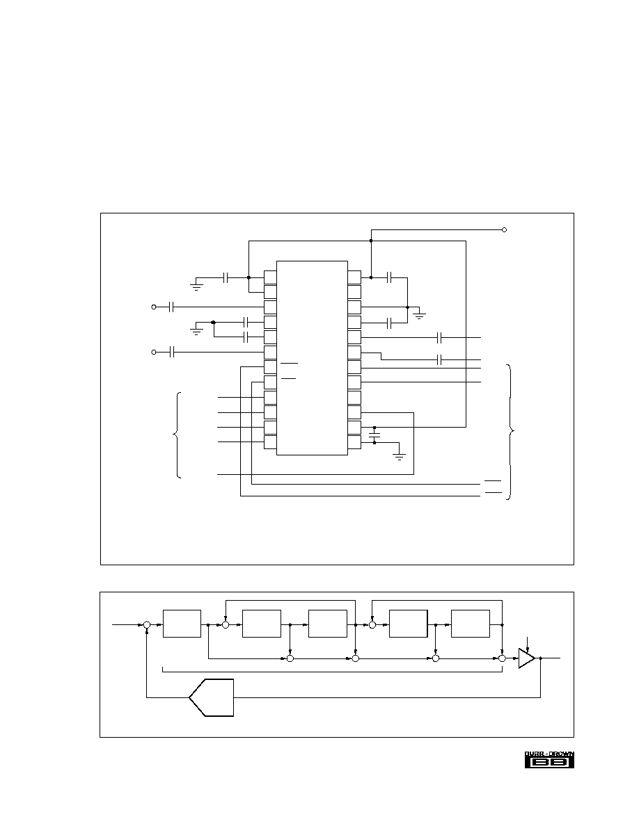
THEORY OF OPERATION
ADC SECTION
The PCM3006 ADC consists of two reference circuits, a
stereo single-to-differential converter, a fully differential
5th-level delta-sigma modulator, a decimation filter (in-
cluding digital high pass), and a serial interface circuit. The
Block Diagram in this data sheet illustrates the architecture
of the ADC section, Figure 1 shows the single-to-differen-
tial converter, and Figure 10 illustrates the architecture of
the 5-level delta-sigma modulator and transfer functions.
FIGURE 9. Typical Connection Diagram for PCM3006.
FIGURE 10. Simplified 5-Level Delta-Sigma Modulator.
+
+
≠
+
+
+
5th SW-CAP
Integrator
4th SW-CAP
Integrator
3rd SW-CAP
Integrator
2nd SW-CAP
Integrator
1st SW-CAP
Integrator
+
+
+
+
≠
+
+
≠
1-Bit
DAC
H(z)
Qn(z)
Analog In
X(z)
Digital Out
Y(z)
Y(z) = STF(z) ∑ X(z) + NTF(z) ∑ Qn(z)
Signal Transfer Function
Noise Transfer Function
STF(z) = H(z) / [1 + H(z)]
NTF(z) = 1/ [1 + H(z)]
Comparator
24
23
22
21
20
19
18
17
16
15
14
13
1
2
3
4
5
6
7
8
9
10
11
12
+
4.7µF
(2)
4.7µF
(2)
+
+
+
+
1µF
(3)
1µF
(3)
Control
Interface
Audio
Interface
+3V Analog V
CC
Rch In
Lch In
SYSCLK
L/R CLK
BIT CLK
DATA OUT
DATA IN
0.1µF
and
10µF
(1)
0.1µF and 10µF
(1)
0.1µF
and 10µF
(1)
4.7µF
(4)
+
4.7µF
(4)
Rch Out
(5)
Lch Out
(5)
DEM0
DEM1
PDAD
PDDA
+
+
4.7µF
(4)
+
PCM3006
V
CC
1
V
CC
1
V
IN
R
V
REF
L
V
REF
R
V
IN
L
PDAD
PDDA
SYSCLK
LRCIN
BCKIN
DOUT
V
CC
2
NC
AGND
V
COM
V
OUT
R
V
OUT
L
DEM0
DEM1
NC
DIN
V
DD
DGND
NOTES: (1) 0.1µF ceramic and 10µF tantalum, typical, depending on power supply quality and pattern layout. (2) 4.7µF typical, gives
settling time with 30ms (4.7µF x 6.4k
) time constant in Power ON and Power-Down OFF period. (3) 1µF typical, gives 5.3Hz cut-off
frequency of input HPF in normal operation and gives settling time with 30ms (1µF x 30k
) time constant in Power ON and Power -Down
OFF period. (4) 4.7µF typical, gives 3.4Hz cut-off frequency of output HPF in normal operation and gives settling time with 47ms (4.7µF x
10k
) time constant in Power ON and Power-Down OFF period. (5) Post low pass filter with R
IN
>10k
, depending on requirement of
system performance.
Æ
16
PCM3006
5-LEVEL
MODULATOR
Frequency (kHz)
Gain (≠dB)
0
≠10
≠20
≠30
≠40
≠50
≠60
≠70
≠80
≠90
≠100
≠110
≠120
≠130
≠140
≠150
0
5
10
15
20
25
30
An internal reference circuit with three external capacitors
provides all reference voltages which are required by the
ADC, which defines the full-scale range for the converter.
The internal single-to-differential voltage converter saves
the design, space and extra parts needed for external cir-
cuitry required by many delta-sigma converters. The internal
full-differential signal processing architecture provides a
wide dynamic range and excellent power supply rejection
performance. The input signal is sampled at 64X
oversampling rate, eliminating the need for a sample-and-
hold circuit, and simplifying anti-alias filtering require-
ments. The 5-level delta-sigma noise shaper consists of five
integrators which use a switched-capacitor topology, a com-
parator and a feedback loop consisting of a one-bit DAC.
The delta-sigma modulator shapes the quantization noise,
shifting it out of the audio band in the frequency domain.
The high order of the modulator enables it to randomize the
modulator outputs, reducing idle tone levels.
The 64f
S
one-bit data stream from the modulator is converted
to 1f
S
16-bit data words by the decimation filter, which also
acts as a low pass filter to remove the shaped quantization
noise. The DC components are removed by a high pass filter
function contained within the decimation filter.
THEORY OF OPERATION
DAC SECTION
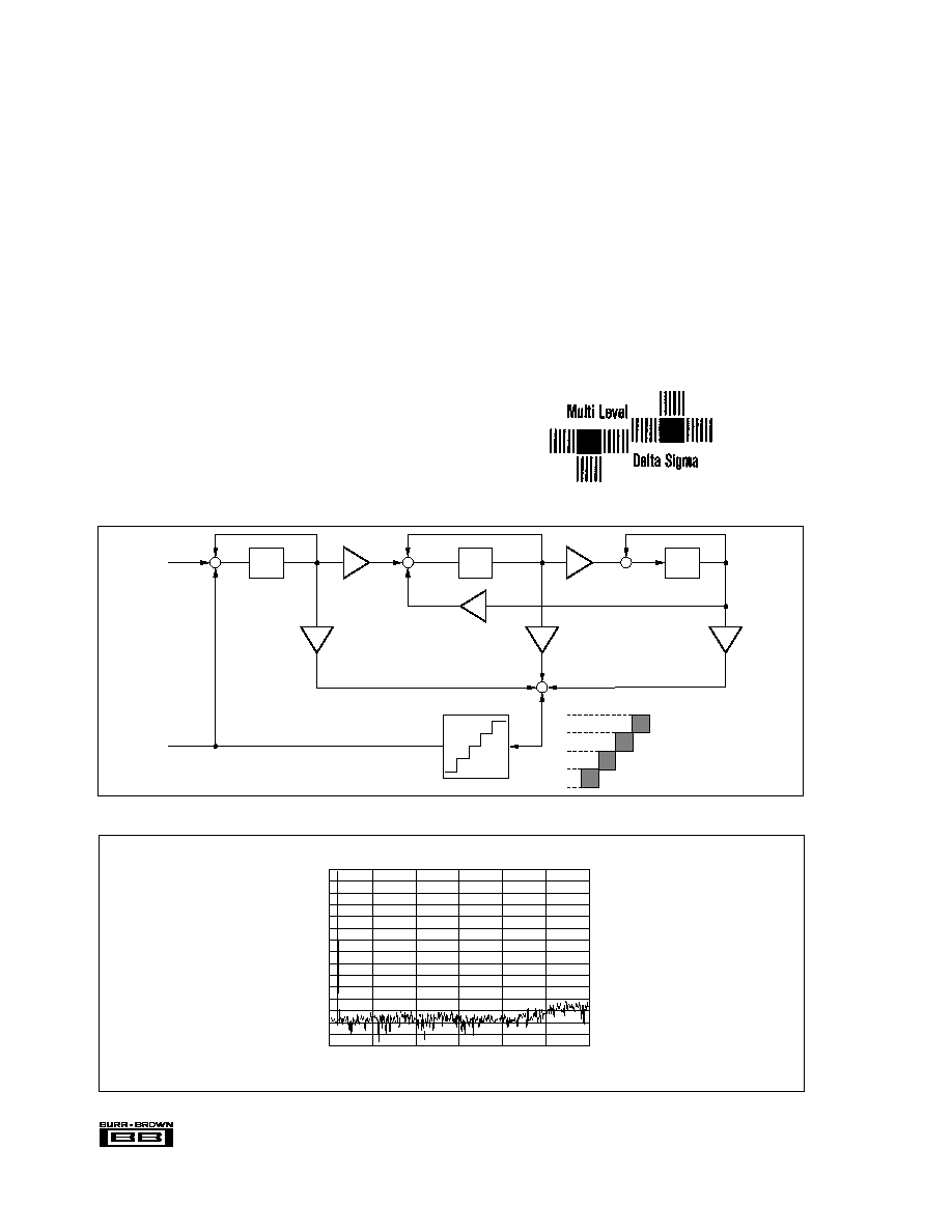
The delta-sigma DAC section of PCM3006 is based on a 5-
level amplitude quantizer and a 3rd-order noise shaper. This
section converts the oversampled input data to 5-level delta-
sigma format. A block diagram of the 5-level delta-sigma
modulator is shown in Figure 11. This 5-level delta-sigma
modulator has the advantage of stability and clock jitter
sensitivity over the typical one-bit (2 level) delta-sigma
modulator. The combined oversampling rate of the delta-
sigma modulator and the internal 8X interpolation filter is
64f
S
for a 256f
S
system clock. The theoretical quantization
noise performance of the 5-level delta-sigma modulator is
shown in Figure 12.
FIGURE 11. 5-Level
Modulator Block Diagram.
FIGURE 12. Quantization Noise Spectrum.
Out
64f
S
(256f
S
)
In
8f
S
16-Bit
+
+
+
4
3
2
1
0
5-level Quantizer
+
≠
+
Z
≠1
+
≠
+
Z
≠1
+
+
Z
≠1

PACKAGING INFORMATION
ORDERABLE DEVICE
STATUS(1)
PACKAGE TYPE
PACKAGE DRAWING
PINS
PACKAGE QTY
PCM3006T
ACTIVE
SSOP
DCV
24
128
PCM3006T/2K
ACTIVE
SSOP
DCV
24
2000
(1) The marketing status values are defined as follows:
ACTIVE: Product device recommended for new designs.
LIFEBUY: TI has announced that the device will be discontinued, and a lifetime-buy period is in effect.
NRND: Not recommended for new designs. Device is in production to support existing customers, but TI does not recommend using this part in
a new design.
PREVIEW: Device has been announced but is not in production. Samples may or may not be available.
OBSOLETE: TI has discontinued the production of the device.
PACKAGE OPTION ADDENDUM
www.ti.com
3-Oct-2003

IMPORTANT NOTICE
Texas Instruments Incorporated and its subsidiaries (TI) reserve the right to make corrections, modifications,
enhancements, improvements, and other changes to its products and services at any time and to discontinue
any product or service without notice. Customers should obtain the latest relevant information before placing
orders and should verify that such information is current and complete. All products are sold subject to TI's terms
and conditions of sale supplied at the time of order acknowledgment.
TI warrants performance of its hardware products to the specifications applicable at the time of sale in
accordance with TI's standard warranty. Testing and other quality control techniques are used to the extent TI
deems necessary to support this warranty. Except where mandated by government requirements, testing of all
parameters of each product is not necessarily performed.
TI assumes no liability for applications assistance or customer product design. Customers are responsible for
their products and applications using TI components. To minimize the risks associated with customer products
and applications, customers should provide adequate design and operating safeguards.
TI does not warrant or represent that any license, either express or implied, is granted under any TI patent right,
copyright, mask work right, or other TI intellectual property right relating to any combination, machine, or process
in which TI products or services are used. Information published by TI regarding third-party products or services
does not constitute a license from TI to use such products or services or a warranty or endorsement thereof.
Use of such information may require a license from a third party under the patents or other intellectual property
of the third party, or a license from TI under the patents or other intellectual property of TI.
Reproduction of information in TI data books or data sheets is permissible only if reproduction is without
alteration and is accompanied by all associated warranties, conditions, limitations, and notices. Reproduction
of this information with alteration is an unfair and deceptive business practice. TI is not responsible or liable for
such altered documentation.
Resale of TI products or services with statements different from or beyond the parameters stated by TI for that
product or service voids all express and any implied warranties for the associated TI product or service and
is an unfair and deceptive business practice. TI is not responsible or liable for any such statements.
Following are URLs where you can obtain information on other Texas Instruments products and application
solutions:
Products
Applications
Amplifiers
amplifier.ti.com
Audio
www.ti.com/audio
Data Converters
dataconverter.ti.com
Automotive
www.ti.com/automotive
DSP
dsp.ti.com
Broadband
www.ti.com/broadband
Interface
interface.ti.com
Digital Control
www.ti.com/digitalcontrol
Logic
logic.ti.com
Military
www.ti.com/military
Power Mgmt
power.ti.com
Optical Networking
www.ti.com/opticalnetwork
Microcontrollers
microcontroller.ti.com
Security
www.ti.com/security
Telephony
www.ti.com/telephony
Video & Imaging
www.ti.com/video
Wireless
www.ti.com/wireless
Mailing Address:
Texas Instruments
Post Office Box 655303 Dallas, Texas 75265
Copyright
2003, Texas Instruments Incorporated