 | –≠–ª–µ–∫—Ç—Ä–æ–Ω–Ω—ã–π –∫–æ–º–ø–æ–Ω–µ–Ω—Ç: PCM3008T | –°–∫–∞—á–∞—Ç—å:  PDF PDF  ZIP ZIP |
PCM3008
SLAS332 ≠ APRIL 2001
LOW POWER AND LOW VOLTAGE 16-BIT, SINGLE-ENDED
ANALOG INPUT/OUTPUT STEREO AUDIO CODEC
1
www.ti.com
FEATURES
D
16-Bit Delta-Sigma ADC and DAC
D
Stereo ADC:
≠ Single-Ended Voltage Input
≠ Anti-Aliasing Filter Included
≠ High Performance
≠ THD+N: ≠84 dB
≠ SNR: 88 dB
≠ Dynamic Range: 88 dB
≠ 1/64
◊
Decimation Digital Filter
≠ Passband Ripple:
±
0.05 dB
≠ Stopband Attenuation: ≠65 dB
≠ Digital HPF Included
D
Stereo DAC:
≠ Single-Ended Voltage Output
≠ Analog LPF and FIR Filter Included
≠ High Performance
≠ THD+N: ≠88 dB
≠ SNR: 92 dB
≠ Dynamic Range: 92 dB
≠ 8
◊
Oversampling Digital Filter
≠ Passband Ripple:
±
0.1 dB
≠ Stopband Attenuation: ≠43 dB
D
Audio Data Format:
≠ ADC: 16-bit, Left-Justified
≠ DAC: 16-bit, Right-Justified
D
Special Built-In Functions:
≠ Digital De-Emphasis: 32, 44.1, 48 kHz
≠ ADC/DAC Independent Power Down With
Pop-Noise Free Muting
D
Sampling Rate: 8 kHz to 48 kHz
D
System Clock: 256f
S
, 384f
S
, 512f
S
D
Low Voltage Power Supply:
≠ 2.4 V TYP, 2.1 V MIN to 3.6 V MAX
D
Low Power Dissipation:
≠ 32 mW at V
CC
= 2.4 V
D
Package: 16-Pin TSSOP
APPLICATIONS
D
Digital Video Camera
D
Portable MD Player
D
Other Portable System
DESCRIPTION
The PCM3008 is a low cost single chip 16-bit
stereo audio codec with single-ended analog
voltage input and output.
Both ADCs and DACs employ delta-sigma
modulation with 64-times oversampling. ADCs
include a digital decimation filter and digital high
pass filter. DACs include an 8-times oversampling
digital interpolation filter, digital de-emphasis filter
and pop-noise free muting which works during the
power down ON/OFF sequence. The PCM3008
accepts left-justified format for ADC, and
right-justified format for DAC. Independent
power-down modes for ADC and DAC are
provided.
The PCM3008 is suitable for a wide variety of
cost-sensitive consumer applications where good
performance is required. It is fabricated using a
highly advanced CMOS process and is available
in a small 16-pin TSSOP package.
PRODUCTION DATA information is current as of publication date.
Products conform to specifications per the terms of Texas Instruments
standard warranty. Production processing does not necessarily include
testing of all parameters.
Copyright
2001, Texas Instruments Incorporated
Please be aware that an important notice concerning availability, standard warranty, and use in critical applications of
Texas Instruments semiconductor products and disclaimers thereto appears at the end of this data sheet.
PCM3008
SLAS332 ≠ APRIL 2001
2
www.ti.com
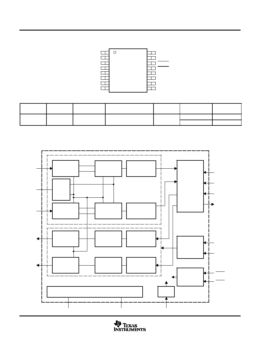
1
2
3
4
5
6
7
8
16
15
14
13
12
11
10
9
V
COM
V
IN
R
V
IN
L
GND
V
CC
DEM0
DEM1
DOUT
V
OUT
R
V
OUT
L
PDDA
PDAD
BCK
SYSCK
LRCK
DIN
PCM3008
PACKAGE
(TOP VIEW)
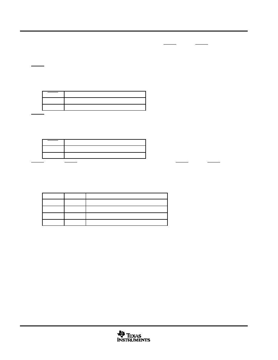
PACKAGE/ORDERING INFORMATION
PRODUCT
PACKAGE
PACKAGE
DRAWING
NUMBER
OPERATION
TEMPERATURE RANGE
PACKAGE
MARKING
ORDERING
NUMBER(1)
TRANSPORT
MEDIA
{
∞
∞
PCM3008T
Rails
PCM3008T
TSSOP≠16
ZZ363
{
≠25
∞
C to +85
∞
C
PCM3008T
PCM3008T/2K
Tape and Reel
TI equivalent no. 4040064.
NOTE: Models with a slash (/) are available only in tape and reel in the quantities indicated (e.g., /2K indicates 2000 devices per reel). Ordering
2000 pieces of PCM3008T/2K will get a single 2000-piece tape and reel.
block diagram
Clock
Power Supply
Reference
ADC
DAC
Analog
Front-End
Circuit
Delta-Sigma
Modulator
+
≠
Decimation
and
High Pass Filter
Serial
Interface
Analog
Front-End
Circuit
Delta-Sigma
Modulator
Decimation
and
High Pass Filter
+
≠
Analog
Low-Pass
Filter
Analog
Low-Pass
Filter
Delta-Sigma
Modulator
Delta-Sigma
Modulator
Interpolation
Filter
8
◊
Oversampling
Interpolation
Filter
8
◊
Oversampling
De-Emphasis
Control
Power Down
Control
VINL
VCOM
VINR
VOUTL
VOUTR
VCC
GND
SYSCK
LRCK
BCK
DIN
DOUT
DEM0
DEM1
PDDA
PDAD

PCM3008
SLAS332 ≠ APRIL 2001
3
www.ti.com
_
+
_
+
Delta
Sigma
Modulator
+
≠
30 k
2
1
VINR
VCOM
+
0.47
µ
F
+
1
µ
F
Reference
Figure 1. Analog Front-End (right-channel)
Terminal Assignments
TERMINAL
NAME
NO.
I/O
DESCRIPTION
VCOM
1
≠
ADC/DAC common decouple (see Note 1)
VINR
2
I
ADC analog input, R-channel.
VINL
3
I
ADC analog input, L-channel.
GND
4
≠
Ground.
VCC
5
≠
Power supply.
DEM0
6
I
De-emphasis control 0 (see Note 2)
DEM1
7
I
De-emphasis control 1 (see Note 2)
DOUT
8
O
Data output
DIN
9
I
Data input (see Note 2)
LRCK
10
I
Sampling clock input (see Note 2)
SYSCK
11
I
System clock input (see Note 2)
BCK
12
I
Bit clock input (see Note 2)
PDAD
13
I
ADC power down, active low (see Note 2)
PDDA
14
I
DAC power down, active low (see Note 2)
VOUTL
15
O
DAC analog output, L-channel.
VOUTR
16
O
DAC analog output, R-channel.
NOTES:
1. Connect decouple capacitor to GND.
2. Schmitt trigger input, open state can not be allowed because of no internal pullup or pulldown.

PCM3008
SLAS332 ≠ APRIL 2001
4
www.ti.com
absolute maximum ratings over operating free-air temperature (unless otherwise noted)
Supply voltage, V
CC
4 V
. . . . . . . . . . . . . . . . . . . . . . . . . . . . . . . . . . . . . . . . . . . . . . . . . . . . . . . . . . . . . . . . . . . . . . . . .
Digital input voltage: DEM0, DEM1, DIN, LRCK, SYSCK, BCK, PDAL, PDDA
≠0.3 V to 4 V
. . . . . . . . . . . . . .
DOUT
≠0.3 V to V
CC
+0.3 V
. . . . . . . . . . . . . . . . . . . . . . . . . . . . . . . . . . . . . . . . . . . . . . . . . .
Analog input voltage
≠0.3 V to V
CC
+0.3 V
. . . . . . . . . . . . . . . . . . . . . . . . . . . . . . . . . . . . . . . . . . . . . . . . . . . . . . . . .
Input current (any pins except supplies)
±
10 mA
. . . . . . . . . . . . . . . . . . . . . . . . . . . . . . . . . . . . . . . . . . . . . . . . . . . .
Ambient temperature under bias
≠ 40
∞
C to 125
∞
C
. . . . . . . . . . . . . . . . . . . . . . . . . . . . . . . . . . . . . . . . . . . . . . . . . . . .
Storage temperature
≠ 55
∞
C to 150
∞
C
. . . . . . . . . . . . . . . . . . . . . . . . . . . . . . . . . . . . . . . . . . . . . . . . . . . . . . . . . . . . . .
Junction temperature
150
∞
C
. . . . . . . . . . . . . . . . . . . . . . . . . . . . . . . . . . . . . . . . . . . . . . . . . . . . . . . . . . . . . . . . . . . . .
Lead temperature (soldering)
260
∞
C, 5 s
. . . . . . . . . . . . . . . . . . . . . . . . . . . . . . . . . . . . . . . . . . . . . . . . . . . . . . . . . . .
Package temperature (IR reflow, peak)
235
∞
C, 10 s
. . . . . . . . . . . . . . . . . . . . . . . . . . . . . . . . . . . . . . . . . . . . . . . . .
Stresses beyond those listed under "absolute maximum ratings" may cause permanent damage to the device. These are stress ratings only, and
functional operation of the device at these or any other conditions beyond those indicated under "recommended operating conditions" is not
implied. Exposure to absolute-maximum-rated conditions for extended periods may affect device reliability.
PCM3008
SLAS332 ≠ APRIL 2001
5
www.ti.com
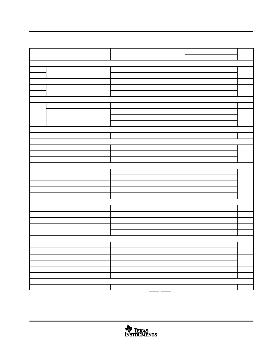
electrical characteristics, all specifications at T
A
= 25
∞
C, V
CC
= 2.4 V, f
s
= 44.1 kHz,
system clock = 384f
s
, f
IN
= 1 kHz, 16-bit data, (unless otherwise noted)
PCM3008T
PARAMETER
TEST CONDITIONS
MIN
TYP
MAX
UNIT
DIGITAL INPUT/OUTPUT
VIH(3)
0.7 VCC
3.6
VIL(3)
Input logic level
0.3VCC
VDC
IIN(3)
Input logic current
±
10
µ
A
VOH(4)
IO = ≠400
µ
A
VCC≠0.2
VOL(4)
Output logic level
IO = 400
µ
A
0.2
VDC
CLOCK FREQUENCY
Sampling frequency
8
44.1
48
kHz
256 fs
2.0480
11.2896
12.2880
fs
System clock frequency
384 fs
3.0720
16.9344
18.4320
MHz
System clock frequency
512 fs
4.0960
22.5792
24.5760
MHz
ADC CHARACTERISTICS
Resolution
16
Bits
DC ACCURACY
Gain mismatch channel to channel
±
1
±
5
Gain error
±
2
±
10
% of
Bipolar zero error
±
0
FSR
DYNAMIC PERFORMANCE(5)
VIN = ≠0.5 dB
≠84
≠74
THD+N
VIN = ≠60 dB
≠26
Dynamic range
A-weighted
82
88
dB
S/N ratio
A-weighted
82
88
dB
Channel separation
80
86
ANALOG INPUT
Input voltage
0.6 VCC
Vp≠p
Center voltage
0.5 VCC
V
Input impedance
30
k
≠3 dB
150
kHz
Antialiasing filter frequency response
fIN = 20 kHz
≠0.08
dB
DIGITAL FILTER PERFORMANCE
Passband
0.454 fs
Stopband
0.583 fs
Hz
Passband ripple
±
0.05
Stopband attenuation
≠65
dB
Delay time
17.4 fs
s
HPF frequency response
≠3 dB
0.078 fs
mHz
DAC CHARACTERISTICS
Resolution
16
Bits
NOTES:
3. Pins 6, 7, 9, 10≠14: DEM0, DEMI, DIN, LRCK, SYSCK, BCK, PDAD, PDDA, (Schmitt trigger input, 3.3 V tolerant.
4. Pin 8: DOUT
5. fIN = 1 kHz, using audio precision system II, RMS mode with 20 kHz LPF, 400 Hz HPF in calculation.

PCM3008
SLAS332 ≠ APRIL 2001
6
www.ti.com
electrical characteristics, all specifications at T
A
= 25
∞
C, V
CC
= 2.4 V, f
s
= 44.1 kHz,
system clock = 384f
s
, f
IN
= 1 kHz, 16-bit data, (unless otherwise noted) (continued)
PCM3008T
PARAMETER
TEST CONDITIONS
MIN
TYP
MAX
UNIT
DC ACCURACY
Gain mismatch channel to channel
±
1
±
5
Gain error
±
2
±
10
%of
Bipolar zero error
±
2
FSR
DYNAMIC PERFORMANCE(6)
VOUT = 0 dB
≠88
≠78
THD+N
VOUT = ≠60 dB
≠30
Dynamic range
EIAJ, A-weighted
86
92
dB
S/N ratio
EIAJ, A-weighted
86
92
dB
Channel separation
84
90
ANALOG OUTPUT
Output voltage
0.6 VCC
Vp≠p
Center voltage
0.5 VCC
V
Load impedance
AC coupling
10
k
≠3 dB
250
kHz
LPF frequency response
fIN = 20 kHz
≠0.03
dB
DIGITAL FILTER PERFORMANCE
Passband
0.445 fs
Stopband
0.555 fs
Hz
Passband ripple
±
0.1
Stopband attenuation
≠43
dB
Delay time
14.3 fs
s
POWER SUPPLY REQUIREMENTS
VCC
Voltage range
2.1
2.4
3.6
VDC
ADC, DAC operation,
13.2
17
ADC operation
8.1
10.5
mA
Supply current
DAC operation
VCC = 2.4 V
5.6
7.5
mA
ADC, DAC power down(7)
20
50
µ
A
ADC, DAC operation,
31.7
40.8
ADC operation
19.4
25.2
mW
Power dissipation
DAC operation
VCC = 2.4 V
13.4
18
mW
ADC, DAC power down(7)
48
120
µ
W
TEMPERATURE RANGE
fs > 24 kHz
≠25
85
∞
Operation temperature
VCC = VMIN to VMAX
fs < 24 kHz
≠25
70
∞
C
JA
Thermal resistance
16-pin TSSOP
150
∞
C/W
6. fIN = 1 kHz, using audio precision system II, RMS mode with 20 kHz LPF, 400 Hz HPF.
7. SYSCK, BCK, LRCK are stopped.
PCM3008
SLAS332 ≠ APRIL 2001
7
www.ti.com
theory of operation
ADC section
The PCM3008 ADC consists of a reference circuit, a stereo single-to-differential converter, a stereo fully
differential 5th-order delta-sigma modulator, a digital decimation filter with high pass filter function and a serial
interface circuit. The block diagram in this data sheet illustrates the architecture of the ADC section and Figure
1 shows the single-to-differential converter.
An internal reference circuit with one external capacitor provides all reference voltages required by the ADC
and DAC. The internal single-to-differential voltage converter saves the design, space and extra parts needed
for external circuitry required by many delta-sigma converters. The internal full-differential signal processing
architecture provides a wide dynamic range and excellent power supply rejection performance. The input signal
is sampled at 64
◊
oversampling rate, eliminating the need for a sample-and-hold circuit, and simplifying
anti-alias filtering requirements. The 5th-order delta-sigma noise shaper consists of five integrators that use a
switched-capacitor topology, a comparator and a feedback loop consisting of a one-bit DAC. The delta-sigma
modulator shapes the quantization noise, shifting it out of the audio band in the frequency domain.
The 64f
s
one-bit data stream from the modulator is converted to 1f
s
16-bit data words by the decimation filter,
which also acts as a low pass filter to remove the shaped quantization noise. The dc components are removed
by a high pass filter function contained within the decimation filter.
DAC section
The PCM3008 DAC consists of a serial interface circuit, a 8
◊
digital interpolation filter with de-emphasis filter
function, a stereo 5th-order delta-sigma modulator, and a stereo analog FIR filter with LPF and output buffer
amplifier. The block diagram in this data sheet illustrates the architecture of the DAC section. 1f
s
16-bit audio
data is converted to 8f
s
18-bit data by an 8
◊
oversampling interpolation filter, and then converted to 64f
s
one-bit
data by delta-sigma modulator. One-bit digital data is converted to an analog signal by a current source D to
A, and then high frequency components of the shaped quantization noise out of band is reduced by the analog
FIR filter and LPF. The fade in, fade out function in digital domain, and V
OUT
control circuit in analog domain
provide a pop-noise free muting function that is required for the power down on/off control sequence.
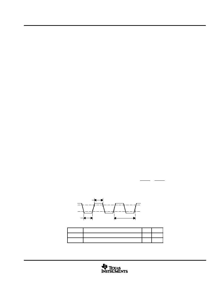
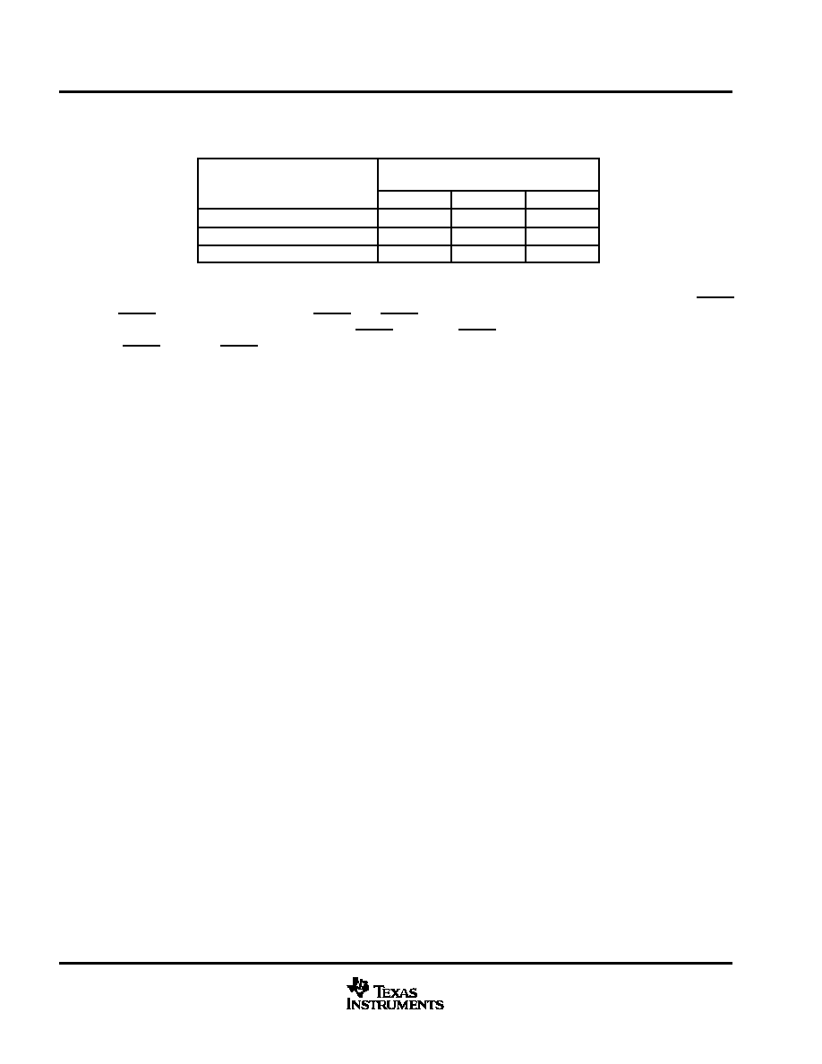
system clock
The system clock for PCM3008 must be either 256f
s
, 384f
s
or 512f
s
, where f
s
is the audio sampling frequency.
The system clock must be supplied on SYSCK (pin 11). PCM3008 also has a system clock detection circuit that
automatically senses 256f
s
, 384f
s
or 512f
s
mode, and when 384f
s
or 512f
s
system clock is used, the clock is
divided into 256f
s
automatically. The 256f
s
clock is used to operate the digital filter and the modulator. The
system clock must be supplied whenever power is applied and either PDAD or PDDA is HIGH, as the PCM3008
uses dynamic circuits internally. Table 1 lists the relationship of typical sampling frequency and system clock
frequency, and Figure 2 illustrates the system clock timing.
tSCKL
1/256 fs, 1/384 fs or 1/512 fs
0.7 VCC
0.3 VCC
tSCKH
H
L
SYSCK
SYMBOL
DEFINITION
MIN
UNIT
tSCKH
System clock pulse width HIGH
15
ns
tSCKL
System clock pulse width LOW
15
ns
Figure 2. System Clock Timing
PCM3008
SLAS332 ≠ APRIL 2001
8
www.ti.com
system clock (continued)
Table 1. System Clock Frequencies
SAMPLING RATE FREQUENCY
SYSTEM CLOCK FREQUENCY
(MHz)
(kHz)
256fs
384fs
512fs
32.0
8.1920
12.2880
16.3840
44.1
11.2896
16.9340
22.5792
48.0
12.2880
18.4320
24.5760
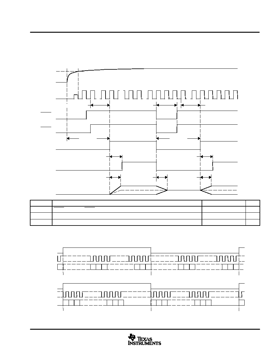
reset
The ADC and DAC portions of the PCM3008 can be reset simultaneously by the power down control pins, PDAD
and PDDA. This external reset using PDAD and PDDA must be always done at least once after the power is
applied. Internal state is kept in reset during PDAD = low and PDDA = low and for 1024 system clock counts
after PDAD = high or PDDA = high, and then the initialization sequence for ADC and DAC is started. For the
ADC, DOUT is kept in ZERO during the initialization sequence and DOUT outputs normal data corresponding
to the input analog signal after t
ADCDLY1
. In the case of the DAC, the fade-in function is started, the signal level
on V
OUT
increases gradually and reaches to full level corresponding to the input digital signal after t
DACDLY1
.
The following figure illustrates the reset timing for power-on and the ADC/DAC output response for the power-on
and reset sequence.
PCM3008
SLAS332 ≠ APRIL 2001
9
www.ti.com
PCM audio interface
Digital audio data is interfaced to the PCM3008 on LRCK (pin 10), BCK (pin 12), DIN (pin 9), and DOUT (pin
8). PCM3008 can accept 16-bit standard format, right-justified 16 bit for DAC and left-justified 16 bit for ADC.
PCM3008 accepts 3 types of BCK and LRCK combination, with 64, 48 or 32 clocks of BCK in one clock of LRCK.
The following figures illustrate audio data input/output format and timing.
Ready
1
1024 1025
1
1024 1025
ZERO
tRSTB
1024 SYSCK
1024 SYSCK
After
Ready
After
Ready
Reset
Reset
Reset
Release
Reset
Release
tADCDLY1
tADCDLY1
tDACDLY1
tDACDLY1
tDACDLY1
VCOM (0.5 VDD)
2.1 V
0 V
VCC
SYSCK
PDAD
PDDA
Internal
Reset
ADC
DOUT
DAC
VO
SYMBOL
DEFINITION
MIN
TYP
MAX
UNIT
tRSTB
PDAD = LOW and PDDA = LOW pulse width
40
ns
tADCDLY1 Initial delay time
2240/fs
s
tDACDLY1 Fade in, fade out time
2080/fs
s
Figure 3. Power-On Reset Timing
LRCK
BCK
DIN
MSB
LSB
MSB
LSB
BCK
LRCK
Right-Channel
DOUT
MSB
LSB
MSB
LSB
16
1
2
3
14 15 16
1
2
3
14 15 16
14 15 16
1
2
3
14 15 16
1
2
3
1
DAC: 16-Bit, MSB-First, Right-Justified
ADC: 16-Bit, MSB-First, Left-Justified
Right-Channel
Left-Channel
Left-Channel
Figure 4. Audio Data Input/Output Format
PCM3008
SLAS332 ≠ APRIL 2001
10
www.ti.com
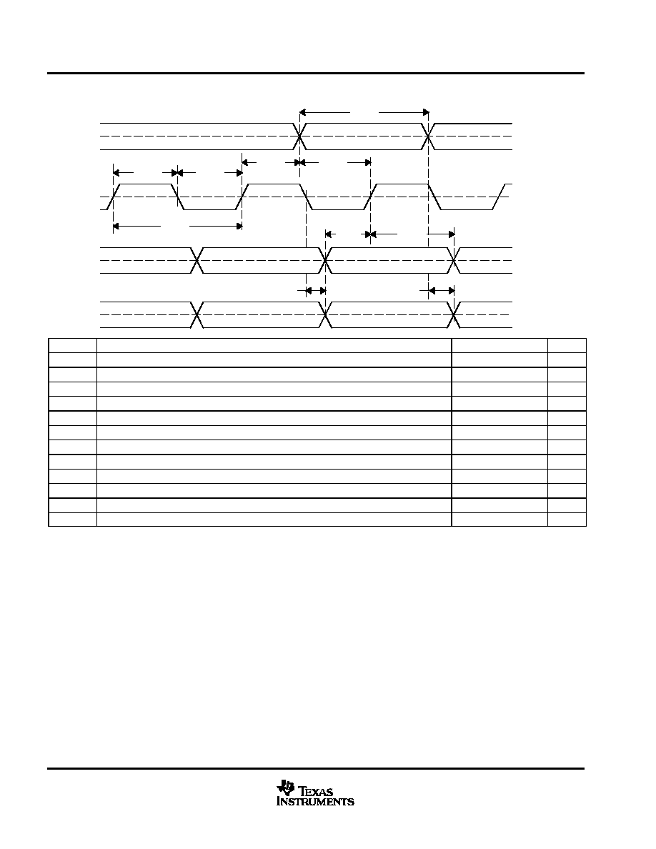
PCM audio interface (continued)
0.5 VCC
0.5 VCC
0.5 VCC
0.5 VCC
tLRP
tBCH
tBCL
tBL
tLB
tBCY
tDIS
tDIH
tBDO
tLDO
LRCK
BCK
DIN
DOUT
SYMBOL
DEFINITION
MIN
TYP
MAX
UNITS
tBCY
BCK pulse cycle time
300
ns
tBCH
BCK pulse width high
120
ns
tBCL
BCK pulse width low
120
ns
tBL
BCK rising edge to LRCK edge
40
ns
tLB
LRCK edge to BCK rising edge
40
ns
tLRP
LRCK pulse width
tBCY
tDIS
DIN setup time
40
ns
tDIH
DIN hold time
40
ns
tBDO
DOUT delay time to BCK falling edge
40
ns
tLDO
DOUT delay time to LRCK edge
40
ns
tR
Rising time of all signals
20
ns
tF
Falling time of all signals
20
ns
Figure 5. Audio Data Input/Output Timing
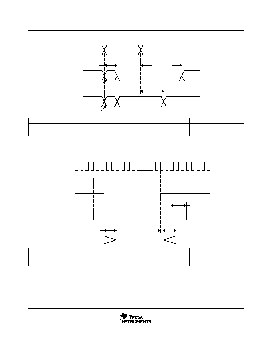
synchronization with digital audio system
PCM3008 operates with LRCK synchronized to the system clock. PCM3008 does not need a specific phase
relationship between LRCK and system clock, but does require the synchronization of LRCK and system clock.
If the relationship between system clock and LRCK changes more than
±
4 BCK during one sample period,
internal operation of DAC halts within 1/f
s
, and analog output is held at the last data until re-synchronization
between system clock and LRCK is completed, and t
DACDLY2
has elapsed.
Internal operation of ADC also halts within 1/f
s
, and digital output is forced into ZERO code until
re-synchronization between system clock and LRCK is completed and t
ADCDLY2
has elapsed. In case of
changes less than
±
4 BCK, re-synchronization does not occur and the above analog/digital output control and
discontinuity do not occur. The following figure illustrates the DAC analog output and ADC digital output for loss
of synchronization. During undefined data periods, some noise may be generated in the audio signal. Also, the
transition of normal to undefined data and undefined data to normal makes a discontinuity of data on analog
and digital output, which also may generate some noise in the audio signal.
PCM3008
SLAS332 ≠ APRIL 2001
11
www.ti.com
synchronization with digital audio system (continued)
Undefined Data
Undefined Data
Within 1/fs
tADCDLY2
tDACDLY2
Synchronous
Asynchronous
Synchronous
Normal
Zero
Normal
Normal
Normal
Last Data
State of
Synchronization
ADC
DOUT
DAC
VO
SYMBOL
DEFINITION
MIN
TYP
MAX
UNIT
tADCDLY2 Delay time from synchronization
32/fs
s
tDACDLY2 Delay time from synchronization
32/fs
s
Figure 6. ADC and DAC Output for Loss of Synchronization
Zero
tADCDLY1
tDACDLY1
1024 SYSCK
tDACDLY1
VCOM (0.5 VCC)
SYSCK
PDAD
PDDA
ADC
DOUT
DAC
VO
SYSCK Can be stopped during
PDAD = LOW and PDDA = LOW.
SYMBOL
DEFINITION
MIN
TYP
MAX
UNIT
tADCDLY1 Initial delay time
2240/fs
s
tDACDLY1 Fade in, fade out time
2080/fs
s
Figure 7. ADC and DAC Output for Power Down Control
PCM3008
SLAS332 ≠ APRIL 2001
12
www.ti.com
function control
The PCM3008 has the following functions which are controlled by PDAD (pin 13), PDDA (pin 14), DEM0 (pin
6) and DEM1 (pin 7).
power-down control
PDAD: ADC power-down control pin places the ADC portion in the lowest power consumption mode. The ADC
operation is stopped by disabling the clock and bias to the ADC portion, and DOUT is forced to zero during ADC
power-down mode. Figure 7 illustrates the ADC DOUT response for ADC power-down ON/OFF. This does not
affect the DAC operation.
PDAD
ADC OPERATION MODE
Low
ADC power down mode enable
High
ADC power down mode disable
PDDA: DAC power-down control pin places the DAC portion in the lowest power consumption mode. The DAC
operation is stopped by disabling the clock and bias to the DAC portion, and V
OUT
is forced to V
COM
(0.5 V
CC
)
during DAC power-down mode. Figure 7 illustrates the DAC V
OUT
response for DAC power-down ON/OFF. This
does not affect the ADC operation.
PDDA
DAC OPERATION MODE
Low
DAC power down mode enable
High
DAC power down mode disable
PDAD = low and PDDA = low places PCM3008 into reset state and either PDAD = high or PDDA = high returns
PCM3008 to operational state.
de-emphasis control
DEM1, DEM0: DAC de-emphasis control pins select the de-emphasis mode as shown below.
DEM1
DEM0
DE-EMPHASIS MODE
Low
Low
De-emphasis 44.1 kHz ON
Low
High
De-emphasis OFF
High
Low
De-emphasis 48 kHz ON
High
High
De-emphasis 32 kHz ON
PCM3008
SLAS332 ≠ APRIL 2001
13
www.ti.com
TYPICAL CHARACTERISTICS
typical circuit connection
The following figure illustrates a typical PCM3008 circuit connection.
VCOM
VINR
VINL
GND
VCC
DEM0
DEM1
DOUT
VOUTR
VOUTL
PDDA
PDAD
BCK
SYSCK
LRCK
DIN
1
2
3
4
5
6
7
8
9
10
11
12
13
14
15
16
+
+
+
Right Channel IN
Left Channel IN
C1(see Note A)
A/D IN
C2(see Note B)
C3(see Note B)
+
C4(see Note C)
2.4 V
De-Emp0
De-Emp1
Control
+
+
C6
(see Note D)
C5
(see Note D)
POST
LPF
(see Note E)
POST
LPF
(see Note E)
Right
Channel OUT
Left
Channel OUT
D/A OUT
D/A ON/OFF
A/D ON/OFF
Bit Clock
System Clock
L/R Clock
D/A IN
A/D OUT
Digital IN/OUT
2.4 V
PDDA
PDAD
(see Note F)
PCM3008
NOTES: A. C1: 0.1
µ
F ceramic and 1
µ
F chemical typical, gives settling time with 15 ms (1
µ
F
◊
15 k
) time constant in power on period.
B. C2, C3: 0.47
µ
F typical, gives 11 Hz cutoff frequency of input HPF in normal operation and gives settling time with 14 ms
(0.47
µ
F
◊
30 k
) time constant in power on and power down off period.
C. C4: 0.1
µ
F ceramic and 10
µ
F chemical typical, depending on power supply quality and pattern layout.
D. C5, C6: 1
µ
F typical, gives 16 Hz cut-off frequency of output HPF in normal operation and gives settling time with 10 ms (1
µ
F
◊
10 k
)
time constant in power on period.
E. Post low pass filter with RIN > 10 k
, depending on requirement of system performance.
F. Power on reset circuit in case of no power-down control requirement.
board design and layout considerations
power supply and grounding (V
CC
, GND)
The analog and digital power supply lines are internally tied, and the analog and digital grounds are internally
tied due to pin count limitation. The power supply V
CC
pin must be bypassed to the GND pin with 0.1
µ
F ceramic
and 10
µ
F chemical capacitors as close to the pins as possible to maximize the dynamic performance of ADC
and DAC.
V
IN
pins
A chemical capacitor from 0.47
µ
F to 4.7
µ
F is recommended as an ac coupling capacitor. Capacitance of 0.47
µ
F gives 11 Hz cut-off frequency at input HPF. If higher full scale input voltage is required, it can be adjusted
by adding only one series resistor to V
IN
pins.
V
COM
input
A 0.1
µ
F ceramic and a 1
µ
F or larger chemical capacitor are recommended between V
COM
and GND to ensure
low source impedance of ADC and DAC common voltage. This capacitor should be located as close as possible
to the V
COM
pin to reduce dynamic errors on the ADC and DAC common voltage.

PCM3008
SLAS332 ≠ APRIL 2001
14
www.ti.com
TYPICAL CHARACTERISTICS
system clock
Dynamic performance may be influenced by the quality of SYSCK. Therefore the duty cycle, jitter and threshold
voltage at the SYSCK pin must be carefully managed. The SYSCK and BCK, LRCK must be supplied whenever
the power is applied and either PDAD or ODDA is HIGH, as the PCM3008 uses dynamic circuits internally.
reset control
The PCM3008 does not have an internal power-on reset circuit. Therefore external reset control by PDAD and
PDDA must always done at least once after the power is turned on. If neither PDAD nor PDDA is needed in the
application, the standard reset circuit which consists of one resistor, one capacitor and one diode is
recommended on PDAD and PDDA pins.
external mute control
Although the PCM3008 has an internal muting function for power-down ON/OFF control, if external muting
control is required, the recommended control sequence is described by External Mute ON, CODEC Power
Down ON, SYSCK stop and resume if necessary, CODEC Power Down OFF and External Mute OFF.
PCM3008
SLAS332 ≠ APRIL 2001
15
www.ti.com
TYPICAL CHARACTERISTICS
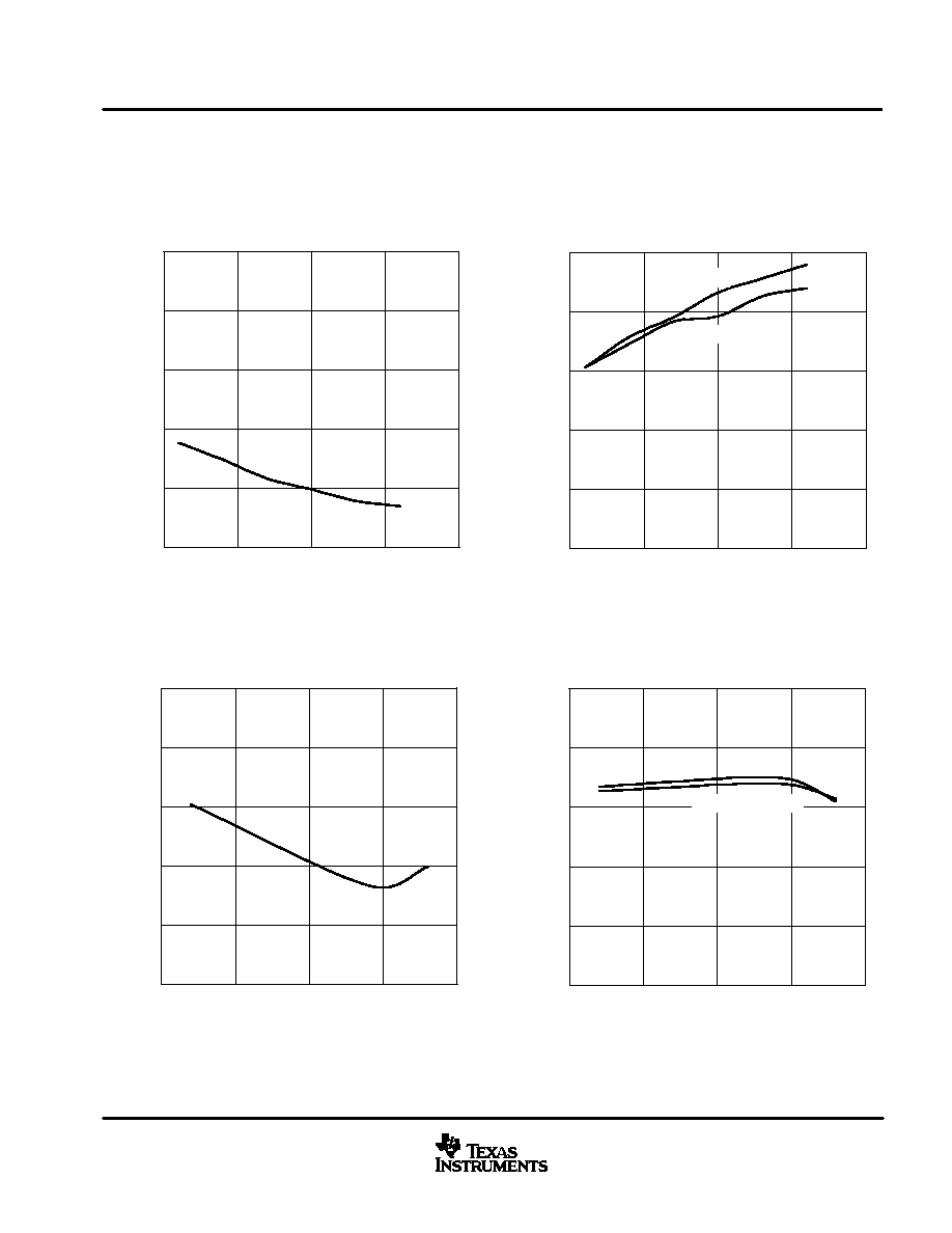
ADC
≠88
≠86
≠84
≠82
≠80
≠78
≠50
≠25
0
25
50
75
100
TOTAL HARMONIC DISTORTION PLUS NOISE AT ≠0.5 dB
vs
FREE-AIR TEMPERATURE
TA ≠ Free-Air Temperature ≠
∞
C
THD+N
≠
T
otal Harmonic Distortion Plus Noise at
≠
0.5 dB
≠
dB
Figure 8
Figure 9
82
84
86
88
90
92
≠50
≠25
0
25
50
75
100
SNR
Dynamic Range
Dynamic Range
And
SNR
≠
dB
DYNAMIC RANGE AND SNR
vs
FREE-AIR TEMPERATURE
TA ≠ Free-Air Temperature ≠
∞
C
≠88
≠86
≠84
≠82
≠80
≠78
2
2.5
3
3.5
4
TOTAL HARMONIC DISTORTION PLUS NOISE AT ≠0.5 dB
vs
SUPPLY VOLTAGE
VCC ≠ Supply Voltage ≠ V
THD+N
≠
T
otal Harmonic Distortion Plus Noise at
≠
0.5 dB
≠
dB
Figure 10
Figure 11
82
84
86
88
90
92
2
2.5
3
3.5
4
SNR
Dynamic Range
Dynamic Range
And
SNR
≠
dB
DYNAMIC RANGE AND SNR
vs
SUPPLY VOLTAGE
VCC ≠ Supply Voltage ≠ V
PCM3008
SLAS332 ≠ APRIL 2001
16
www.ti.com
TYPICAL CHARACTERISTICS
ADC
≠88
≠86
≠84
≠82
≠80
≠78
30
35
40
45
50
TOTAL HARMONIC DISTORTION PLUS NOISE AT ≠0.5 dB
vs
SAMPLING FREQUENCY
fs ≠ Sampling Frequency ≠ kHz
THD+N
≠
T
otal Harmonic Distortion Plus Noise at
≠
0.5 dB
≠
dB
Figure 12
Figure 13
fs ≠ Sampling Frequency ≠ kHz
Dynamic Range
And
SNR
≠
dB
DYNAMIC RANGE AND SNR
vs
SAMPLING FREQUENCY
82
84
86
88
90
92
30
35
40
45
50
SNR
Dynamic Range
DAC
≠92
≠90
≠88
≠86
≠84
≠82
≠50
≠25
0
25
50
75
100
TOTAL HARMONIC DISTORTION PLUS NOISE AT 0 dB
vs
FREE-AIR TEMPERATURE
TA ≠ Free-Air Temperature ≠
∞
C
THD+N
≠
T
otal Harmonic Distortion Plus Noise at 0 dB
≠
dB
Figure 14
Figure 15
86
88
90
92
94
96
≠50
≠25
0
25
50
75
100
SNR
Dynamic Range
Dynamic Range
And
SNR
≠
dB
DYNAMIC RANGE AND SNR
vs
FREE-AIR TEMPERATURE
TA ≠ Free-Air Temperature ≠
∞
C
PCM3008
SLAS332 ≠ APRIL 2001
17
www.ti.com
TYPICAL CHARACTERISTICS
DAC
≠92
≠90
≠88
≠86
≠84
≠82
2
2.5
3
3.5
4
TOTAL HARMONIC DISTORTION PLUS NOISE AT 0 dB
vs
SUPPLY VOLTAGE
VCC ≠ Supply Voltage ≠ V
THD+N
≠
T
otal Harmonic Distortion Plus Noise at 0 dB
≠
dB
Figure 16
Figure 17
86
88
90
92
94
96
2
2.5
3
3.5
4
SNR
Dynamic Range
Dynamic Range
And
SNR
≠
dB
DYNAMIC RANGE AND SNR
vs
SUPPLY VOLTAGE
VCC ≠ Supply Voltage ≠ V
≠92
≠90
≠88
≠86
≠84
≠82
30
35
40
45
50
TOTAL HARMONIC DISTORTION PLUS NOISE AT 0 dB
vs
SAMPLING FREQUENCY
fs ≠ Sampling Frequency ≠ kHz
THD+N
≠
T
otal Harmonic Distortion Plus Noise at 0 dB
≠
dB
Figure 18
Figure 19
86
88
90
92
94
96
30
35
40
45
50
fs ≠ Sampling Frequency ≠ kHz
Dynamic Range
And
SNR
≠
dB
DYNAMIC RANGE AND SNR
vs
SAMPLING FREQUENCY
SNR
Dynamic Range
PCM3008
SLAS332 ≠ APRIL 2001
18
www.ti.com
TYPICAL CHARACTERISTICS
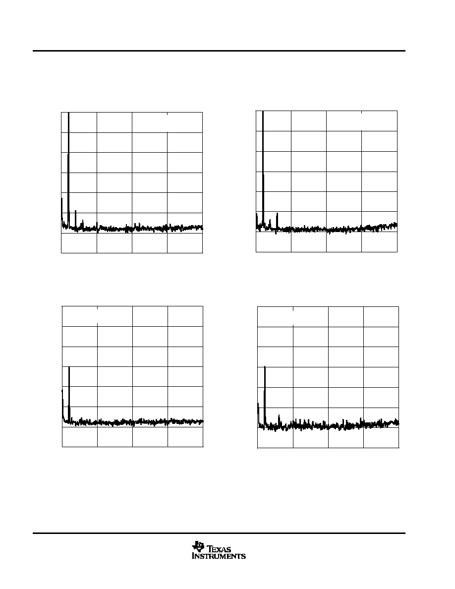
≠140
≠120
≠100
≠80
≠60
≠40
≠20
0
0
5
10
15
20
Amplitude
≠
dB
f ≠ Frequency ≠ kHz
OUTPUT SPECTRUM
≠0.5 dB,
N = 8192
Figure 20
Figure 21
ADC
DAC
≠140
≠120
≠100
≠80
≠60
≠40
≠20
0
0
5
10
15
20
Amplitude
≠
dB
f ≠ Frequency ≠ kHz
OUTPUT SPECTRUM
0 dB,
N = 8192
≠140
≠120
≠100
≠80
≠60
≠40
≠20
0
0
5
10
15
20
Amplitude
≠
dB
f ≠ Frequency ≠ kHz
OUTPUT SPECTRUM
≠60 dB,
N = 8192
Figure 22
Figure 23
≠140
≠120
≠100
≠80
≠60
≠40
≠20
0
0
5
10
15
20
Amplitude
≠
dB
f ≠ Frequency ≠ kHz
OUTPUT SPECTRUM
≠60 dB,
N = 8192
PCM3008
SLAS332 ≠ APRIL 2001
19
www.ti.com
TYPICAL CHARACTERISTICS
Figure 24
Figure 25
ADC
DAC
≠100
≠80
≠60
≠40
≠20
0
≠100
≠80
≠60
≠40
≠20
0
TOTAL HARMONIC DISTORTION PLUS NOISE
vs
SIGNAL LEVEL
Signal Level ≠ dB
THD+N
≠
T
otal Harmonic Distortion Plus Noise
≠
dB
≠100
≠80
≠60
≠40
≠20
0
≠100
≠80
≠60
≠40
≠20
0
TOTAL HARMONIC DISTORTION PLUS NOISE
vs
SIGNAL LEVEL
Signal Level ≠ dB
THD+N
≠
T
otal Harmonic Distortion Plus Noise
≠
dB
Figure 26
0
4
8
12
16
20
2
2.5
3
3.5
4
0
0.4
0.8
1.2
1.6
2
ADC+DAC
ADC
DAC
Power Down
SUPPLY CURRENT
vs
SUPPLY VOLTAGE
VCC ≠ Supply Voltage ≠ V
≠
Supply Current
≠
mA
I CC
≠
Power Down Supply Current
≠
mA
I D
PCM3008
SLAS332 ≠ APRIL 2001
20
www.ti.com
TYPICAL CHARACTERISTICS
0
4
8
12
16
20
0
10
20
30
40
50
0
0.4
0.8
1.2
1.6
2
ADC+DAC
ADC
DAC
Power Down
SUPPLY CURRENT
vs
SAMPLING FREQUENCY
≠
Supply Current
≠
mA
I CC
≠
Power Down Supply Current
≠
mA
I D
fs ≠ Sampling Frequency ≠ kHz
Figure 27
≠140
≠120
≠100
≠80
≠60
≠40
≠20
0
0
20
40
60
80
100
Amplitude
≠
dB
f ≠ Frequency ≠ kHz
DAC OUTBAND NOISE SPECTRUM
BPZ,
N = 8192
Figure 28

PCM3008
SLAS332 ≠ APRIL 2001
21
www.ti.com
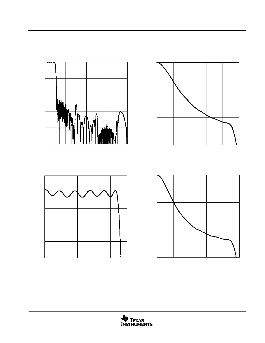
TYPICAL CHARACTERISTICS
ADC digital decimation filter frequency response
≠160
≠120
≠80
≠40
0
0
8
16
24
32
Amplitude
≠
dB
Normalized Frequency ≠ Hz
OVERALL CHARACTERISTIC
x fs
Figure 29
Figure 30
≠100
≠80
≠60
≠40
≠20
0
0
0.2
0.4
0.6
0.8
1
Amplitude
≠
dB
Normalized Frequency ≠ Hz
STOPBAND ATTENUATION
x fs
≠0.8
≠0.6
≠0.4
≠0.2
0
0.2
0
0.1
0.2
0.3
0.4
0.5
Amplitude
≠
dB
Normalized Frequency ≠ Hz
PASSBAND RIPPLE
x fs
≠20
≠16
≠12
≠8
≠4
0
0.46
0.48
0.50
0.52
0.54
Amplitude
≠
dB
Normalized Frequency ≠ Hz
TRANSIENT BAND RESPONSE
x fs
Figure 31
Figure 32

PCM3008
SLAS332 ≠ APRIL 2001
22
www.ti.com
TYPICAL CHARACTERISTICS
digital high pass filter frequency response
≠100
≠80
≠60
≠40
≠20
0
0
0.1
0.2
0.3
0.4
Amplitude
≠
dB
Normalized Frequency ≠ Hz
STOPBAND CHARACTERISTIC
x fs/1000
Figure 33
Figure 34
≠1
≠0.8
≠0.6
≠0.4
≠0.2
0
0
1
2
3
4
Amplitude
≠
dB
Normalized Frequency ≠ Hz
PASSBAND CHARACTERISTIC
x fs/1000
analog antialiasing filter frequency response
≠50
≠40
≠30
≠20
≠10
0
1
10
100
1 k
10 k
Amplitude
≠
dB
f ≠ Frequency ≠ kHz
STOPBAND CHARACTERISTIC
Figure 35
Figure 36
≠1
≠0.8
≠0.6
≠0.4
≠0.2
0
0.01
0.1
1
10
100
Amplitude
≠
dB
PASSBAND CHARACTERISTIC
f ≠ Frequency ≠ kHz
PCM3008
SLAS332 ≠ APRIL 2001
23
www.ti.com
TYPICAL CHARACTERISTICS
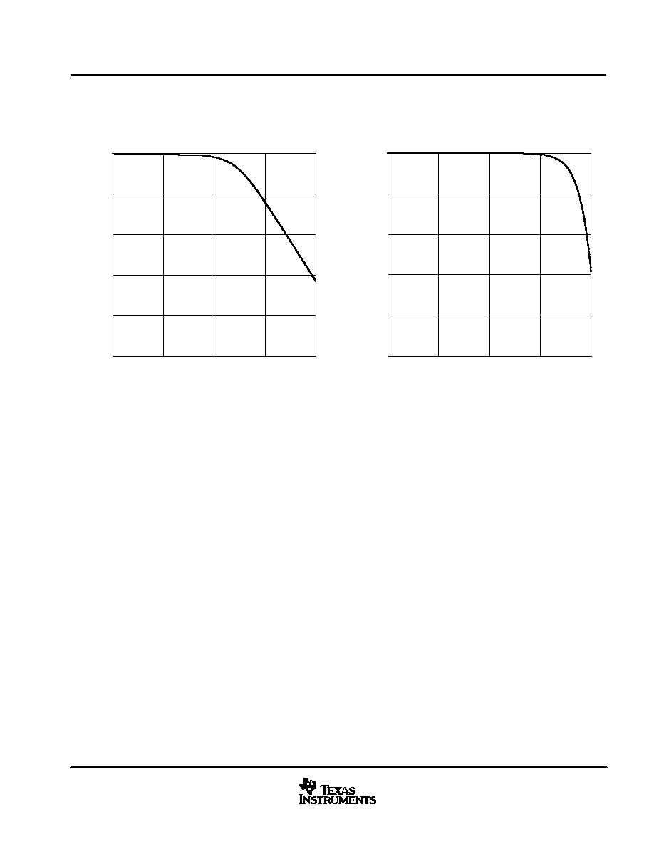
DAC digital interpolation and de-emphasis filter frequency response
≠100
≠80
≠60
≠40
≠20
0
0
1
2
3
4
Amplitude
≠
dB
STOPBAND ATTENUATION
Normalized Frequency ≠ Hz
x fs
Figure 37
Figure 38
≠12
≠8
≠4
0
0
0.1
0.2
0.3
0.4
0.5
Amplitude
≠
dB
DE-EMPHASIS CHARACTERISTIC (32 kHz)
Normalized Frequency ≠ Hz
x fs
≠0.8
≠0.6
≠0.4
≠0.2
0
0.2
0
0.1
0.2
0.3
0.4
0.5
Amplitude
≠
dB
Normalized Frequency ≠ Hz
PASSBAND RIPPLE
x fs
Figure 39
Figure 40
≠12
≠8
≠4
0
0
0.1
0.2
0.3
0.4
0.5
Amplitude
≠
dB
DE-EMPHASIS CHARACTERISTIC (44.1 kHz)
Normalized Frequency ≠ Hz
x fs

PCM3008
SLAS332 ≠ APRIL 2001
24
www.ti.com
TYPICAL CHARACTERISTICS
DAC digital interpolation and de-emphasis filter frequency response (continued)
≠20
≠16
≠12
≠8
≠4
0
0.46
0.48
0.50
0.52
0.54
Amplitude
≠
dB
TRANSIENT BAND RESPONSE
Normalized Frequency ≠ Hz
x fs
Figure 41
Figure 42
≠12
≠8
≠4
0
0
0.1
0.2
0.3
0.4
0.5
Amplitude
≠
dB
DE-EMPHASIS CHARACTERISTIC (48 kHz)
Normalized Frequency ≠ Hz
x fs
analog FIR filter frequency response
≠50
≠40
≠30
≠20
≠10
0
0
8
16
24
32
Amplitude
≠
dB
STOPBAND CHARACTERISTIC
Normalized Frequency ≠ Hz
x fs
Figure 43
Figure 44
≠0.8
≠0.6
≠0.4
≠0.2
0
0.2
0
0.1
0.2
0.3
0.4
0.5
Amplitude
≠
dB
PASSBAND CHARACTERISTIC
Normalized Frequency ≠ Hz
x fs
PCM3008
SLAS332 ≠ APRIL 2001
25
www.ti.com
TYPICAL CHARACTERISTICS
analog low pass filter frequency response
Figure 45
Figure 46
≠50
≠40
≠30
≠20
≠10
0
1
10
100
1 k
10 k
Amplitude
≠
dB
STOPBAND CHARACTERISTIC
f ≠ Frequency ≠ kHz
≠1
≠0.8
≠0.6
≠0.4
≠0.2
0
0.01
0.1
1
10
100
Amplitude
≠
dB
PASSBAND CHARACTERISTIC
f ≠ Frequency ≠ kHz
Æ
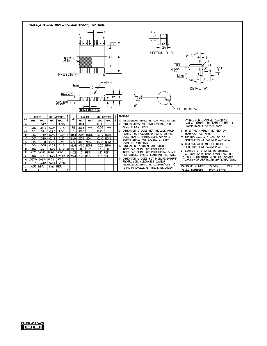
PACKAGE DRAWINGS
MPDS090

IMPORTANT NOTICE
Texas Instruments and its subsidiaries (TI) reserve the right to make changes to their products or to discontinue
any product or service without notice, and advise customers to obtain the latest version of relevant information
to verify, before placing orders, that information being relied on is current and complete. All products are sold
subject to the terms and conditions of sale supplied at the time of order acknowledgment, including those
pertaining to warranty, patent infringement, and limitation of liability.
TI warrants performance of its products to the specifications applicable at the time of sale in accordance with
TI's standard warranty. Testing and other quality control techniques are utilized to the extent TI deems necessary
to support this warranty. Specific testing of all parameters of each device is not necessarily performed, except
those mandated by government requirements.
Customers are responsible for their applications using TI components.
In order to minimize risks associated with the customer's applications, adequate design and operating
safeguards must be provided by the customer to minimize inherent or procedural hazards.
TI assumes no liability for applications assistance or customer product design. TI does not warrant or represent
that any license, either express or implied, is granted under any patent right, copyright, mask work right, or other
intellectual property right of TI covering or relating to any combination, machine, or process in which such
products or services might be or are used. TI's publication of information regarding any third party's products
or services does not constitute TI's approval, license, warranty or endorsement thereof.
Reproduction of information in TI data books or data sheets is permissible only if reproduction is without
alteration and is accompanied by all associated warranties, conditions, limitations and notices. Representation
or reproduction of this information with alteration voids all warranties provided for an associated TI product or
service, is an unfair and deceptive business practice, and TI is not responsible nor liable for any such use.
Resale of TI's products or services with
statements different from or beyond the parameters stated by TI for
that product or service voids all express and any implied warranties for the associated TI product or service,
is an unfair and deceptive business practice, and TI is not responsible nor liable for any such use.
Also see: Standard Terms and Conditions of Sale for Semiconductor Products. www.ti.com/sc/docs/stdterms.htm
Mailing Address:
Texas Instruments
Post Office Box 655303
Dallas, Texas 75265
Copyright
©
2001, Texas Instruments Incorporated